

Page 1
查询TS68882供应商
Features
• Eight General-purpose Floating-point Data Registers, Each Supporting a Full 80-bit
Extended Precision Real Data Format (a 64-bit Mantissa Plus a Sign Bit, and a 15-bit
Signed Exponent)
• A 67-bit Arithmetic Unit to Allow Very Fast Calculations with Intermediate are Precision
Greater than the Extended Precision Format
• A 67-bit Barrel Shifter for High-speed Shifting Operations (for Normalizing etc.)
• Special-purpose Hardware for High-speed Conversion Between Single, Double, and
Extended Formats and the Internal Extended Format
• An Independent State Machine to Control Main Processor Communication for
Pipelined Instruction Processing
• Forty-six Instructions, Including 35 Arithmetic Operations
• Full Conformation to the IEEE 754 Standard, Including All Requirements and
Suggestions
• Support of Functions Not Defined by the IEEE Standard, Including a Full Set of
Trigonometric and Transcendental Functions
• Seven Data Type Types: Byte, Word and Long Integers; Single, Double, and Extended
Precision Real Numbers; and Packed Binary Coded Decimal String Real Numbers
• Twenty-two Constants Available In The On-chip ROM, Including π,e,andPowersof10
• Virtual Memory/Machine Operations
• Efficient Mechanisms for Procedure Calls, Context Switches, and Interrupt Handling
• Fully Concurrent Instruction Execution with the Main Processor
• Fully Concurrent Instruction Execution of Multiple Floating-point Instructions
• Use with any Host Processor, on an 8-, 16- or 32-bit Data Bus
• Available in 16.67, 20, 25 and 33 MHz for T
• V
=5V± 10%
CC
from -55°C to +125°C
c
CMOS
Enhanced
Floating-point
Co-processor
TS68882
Description
The TS68882 enhanced floating-point co-processor is a full implementation of the
IEEE Standard for Binary Floating-Point Arithmetic (754) for use with the THOMSON
TS68000 Family of microprocessors. It is a pin and software compatible upgrade of
the TS68881 with optimized MPU interface that provides over 1.5 times the performance of the TS68881. It is implemented using VLSI technology to give systems
designers the highest possible functionality in a physically small device.
Intended primarily for use as a co-processor to the TS68020/68030 32-bit microprocessor units (MPUs), the TS68882 provides a logical extension to the main MPU
integer data processing capabilities. It does this by providing a very high performance
floating-point arithmetic unit and a set of floating-point data registers that are utilized
in a manner that is analogous to the use of the integer data registers. The TS68882
instruction set is a natural extension of all earlier members of the TS68000 Family, and
supports all of the addressing modes of the host MPU. Due to the flexible bus interface of the TS68000 Family, the TS68882 can be used with any of the MPU devices of
the TS68000 Family, and it may also be used as a peripheral to non-TS68000
processors.
Screening/Quality
This product could be manufactured
in full compliance with either:
• MIL-STD-883 Class B
• DESC 5962-89436
• or According to ATMELGrenoble Standards
R suffix
PGA 68
Ceramic Pin Grid Array
F suffix
CQFP 68
Ceramic Quad Flat Pack
Rev. 2119A–HIREL–04/02
1
Page 2

Introduction The TS68882 is a high-performance floating-point device designed to interface with the
TS68020 or TS68030 as a co-processor. This device fully supports the TS68000 virtual
machine architecture, and is implemented in HCMOS, Atmel’s low power, small geometry process. This process allows CMOS and HMOS (high-density NMOS) gates to be
combined on the same device. CMOS structures are used where speed and low power
is required, and HMOS structures are used where minimum silicon area is desired. The
HCMOS technology enables the TS68882 to be very fast while consuming less power
than comparable HMOS, and still have a reasonably small die size.
With some performance degradation, the TS68882 can also be used as a peripheral
processor in systems where the TS68020 or TS68030 is not the main processor (i.e.,
TS68000, TS68010). The configuration of the TS68882 as a peripheral processor or coprocessor may be completely transparent to user software (i.e., the same object code
may be executed in either configuration).
The architecture of the TS68882 appears to the user as a logical extension of the
TS68000 Family architecture. Coupling of the co-processor interface allows the
TS68020/TS68030 programmer to view the TS68882 registers as though the registers
are resident in the TS68020/TS68030. Thus, a TS68020 or TS68030/TS68882 device
pair appears to be one processor that supports seven floating-point and integer data
types, and has eight integer data registers, eight address registers, and eight floatingpoint data registers.
As shown in Figure 1, the TS68882 is internally divided into four processing elements;
the Bus Interface Unit (BIU), the Conversion Control Unit (CCU), the Execution Control
Unit (ECU), and the Microcode Control Unit (MCU). The BIU communicates with the
main processor, the CCU controls the main processor communications dialog and performs some data conversions, and the ECU and MCU execute most floating-point
calculations.
The BIU contains the co-processor interface registers, and the 32-bit control, and
instruction address registers. In addition to these registers, the register select and
DSACK timing control logic is contained in the BIU. Finally, the status flags used to monitor the status of communications with the main processor are contained in the BIU.
The CCU contains special-purpose hardware that performs conversions between the
single, double, and extended precision memory data formula and the internal data format used by the ECU. It also contains a state machine that controls communications
with the main processor during co-processor interface dialogs.
The eight 80-bit floating-point data registers (FP0-FP7) are located in the ECU. In addition to these registers, the ECU contains a high-speed 67-bit arithmetic unit used for
both mantissa and exponent calculations, a barrel shifter that can shift from 1-bit to 67bits in one machine cycle, and ROM constants (for use by the internal algorithms or user
programs).
The MCU contains the clock generator, a two-level microcoded sequencer that controls
the ECU, the microcode ROM, and self-test circuitry. The built-in self-test capabilities of
the TS68882 enhance reliability and ease manufacturing requirements; however, these
diagnostic functions are not available to the user.
2
TS68882
2119A–HIREL–04/02
Page 3
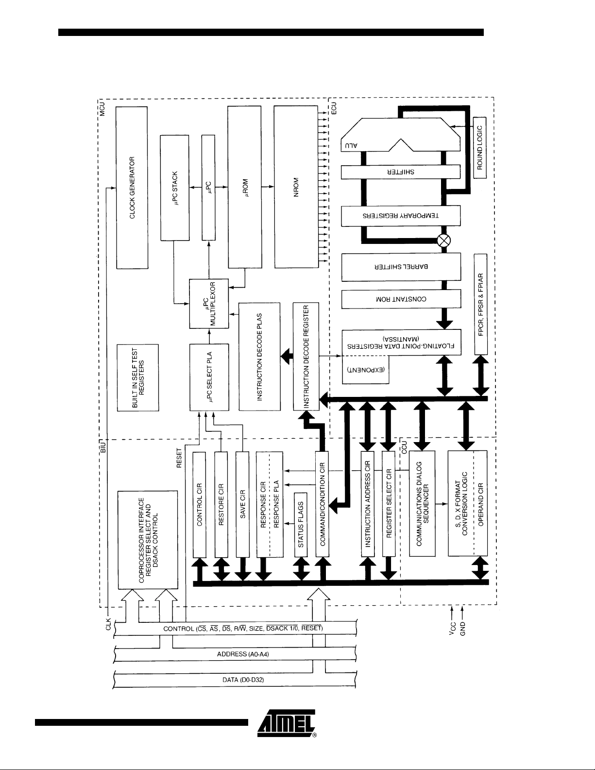
Figure 1. TS68882 Simplified Block
TS68882
2119A–HIREL–04/02
3
Page 4
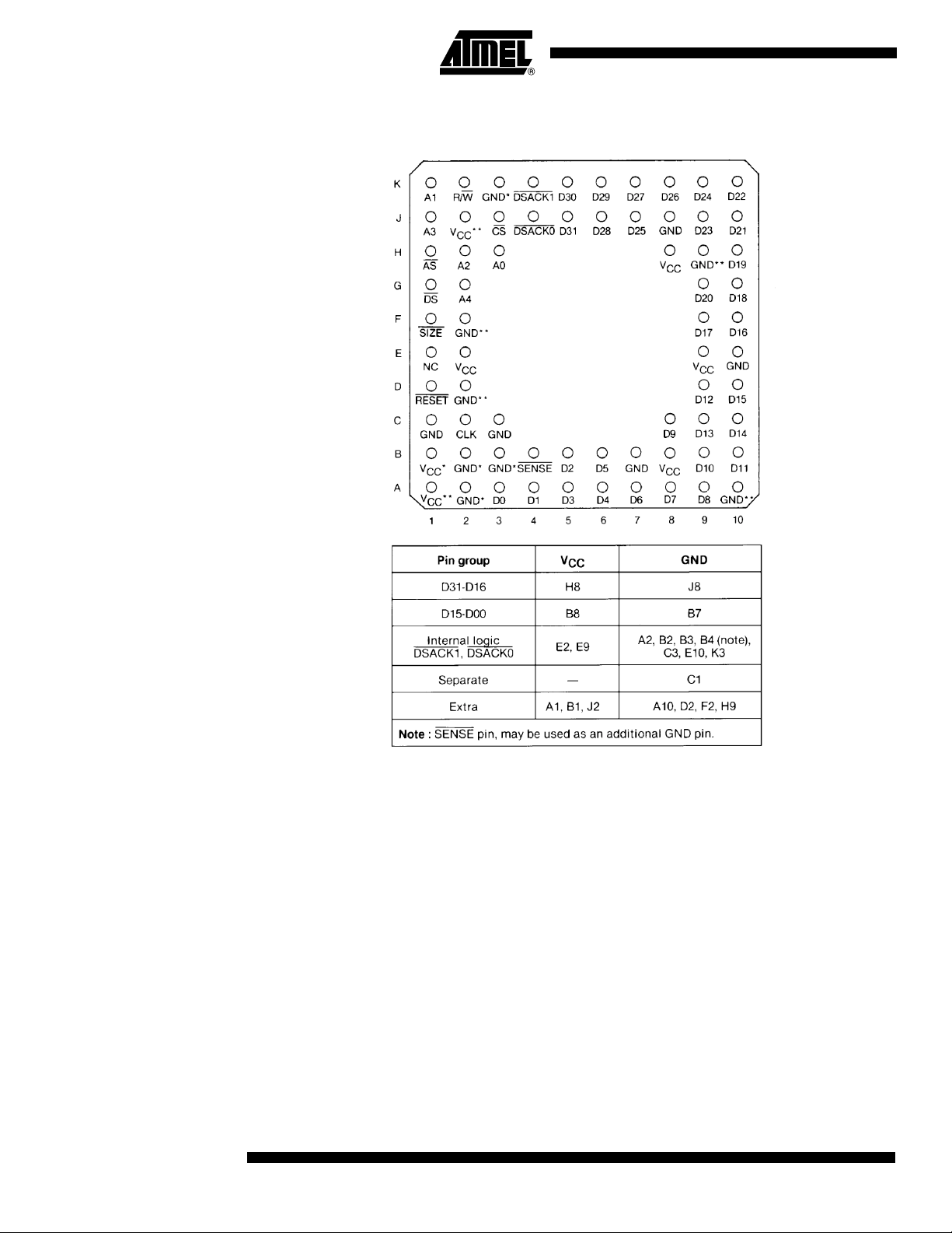
Pin Assignments Figure 2. PGA Terminal Designation
* Reserved for future ATMEL-Grenoble use
4
TS68882
2119A–HIREL–04/02
Page 5
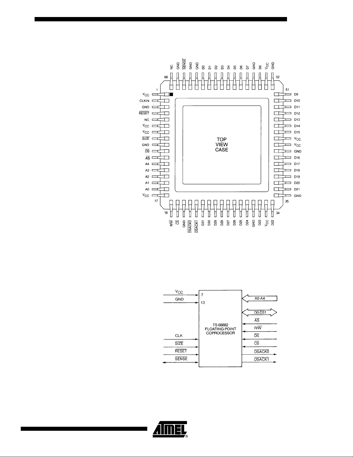
Figure 2b. CQFP Terminal Designation
TS68882
Functional Signal
Descriptions
This section contains a brief description of the input and output signals for the TS68882
floating-point co-processor. The signals are functionally organized into groups as shown
in Figure 3.
Figure 3. TS68882 Input/output Signals
Note: The terms assertion and negation are used extensively. This is done to avoid confusion
when describing “active-low” and “active-high” signals. The term assert or assertion is
used to indicate that a signal is active or true, independent of whether that level is represented by a high or low voltage. The term negate or negation is used to indicate that a
signal is inactive or false.
2119A–HIREL–04/02
5
Page 6
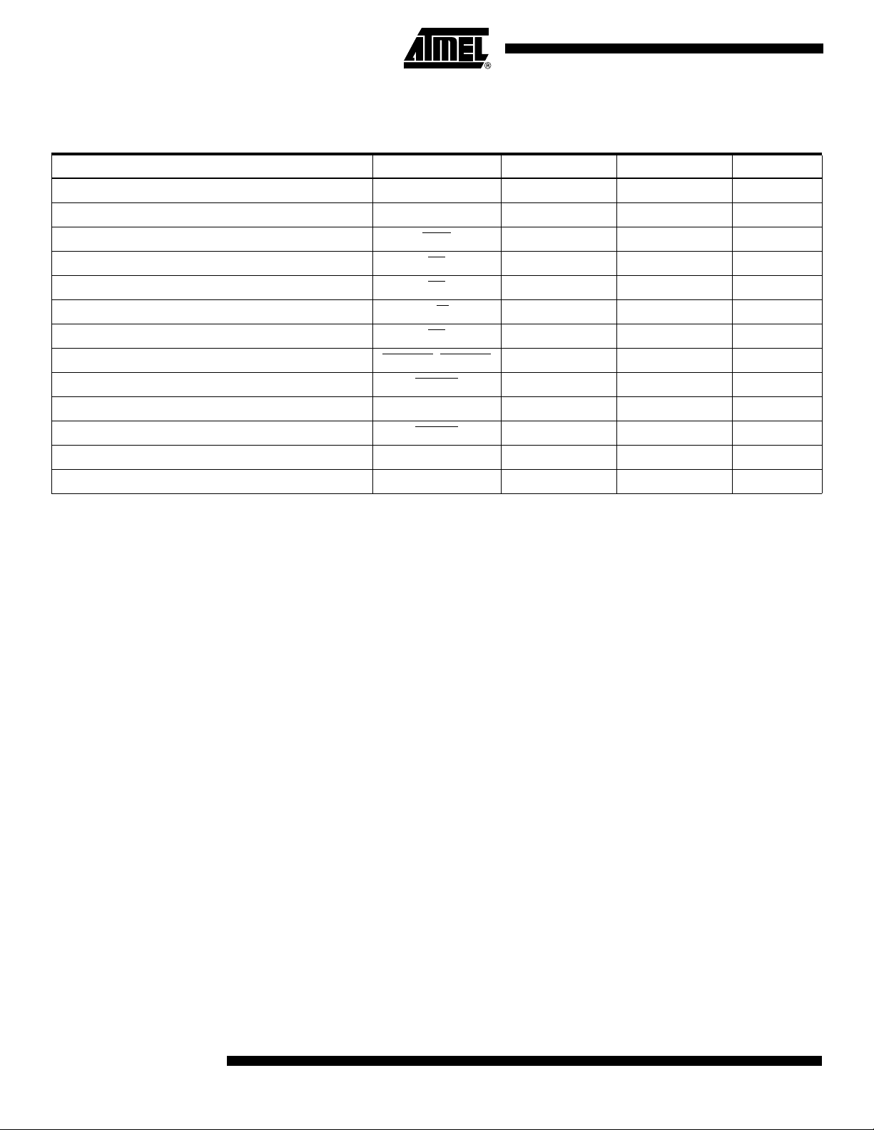
Signal Summary Table 1 provides a summary of all the TS68882 signals described in this section.
Table 1 . Signal Summary
Signal Name Mnemonic Input/Output Active State Three State
Address Bus A0 - A4 Input High
Data Bus D0 - D31 Input/Output High Yes
Size SIZE
Input Low
Address Strobe AS
Chip Select CS
Read/Write R/W
Data Strobe DS
Data Transfer and Size Acknowledge DSACK0
Reset RESET
Clock CLK Input
Sense Device SENSE
Power Input V
Ground GND Input
,DSACK1 Output Low Yes
CC
Input Low
Input Low
Input High/Low
Input Low
Input Low
Input/Output Low No
Input
Detailed
Specifications
Scope This drawing describes the specific requirements for the microprocessor 68882, 16.67,
20 MHz and 25 MHz, in compliance with MIL-STD-883 class B.
Applicable Documents
MIL-STD-883 1. MIL-STD-883: Test Methods And Procedures For Electronics
2. MIL-PRF-38535 Appendix A: General Specifications For Microcircuits
3. Desc Drawing 5962 - 89436xxx
Requirements
General The microcircuits are in accordance with the applicable document and as specified
herein.
Design and Construction
Terminal Connections Depending on the package, the terminal connections shall be as shown in Figure 2 and
Figure 2b.
Lead Material and Finish Lead material and finish shall be any option of MIL-STD-1835.
6
TS68882
2119A–HIREL–04/02
Page 7
TS68882
Package The macrocircuits are packaged in hermetically sealed ceramic packages which are
conform to case outlines of MIL-STD-1835 (when defined):
• 68-PIN SQ.PGA UP PAE Outline
• 68-PIN Ceramic Quad Flat Pack CQFP
The precise case outlines are described on Figure 23 and Figure 24.
Electrical
Characteristics
Table 2 . Absolute Maximum Ratings
Symbol Parameter Test Conditions Min Max Unit
V
P
CC
V
I
DMAX
Supply Voltage -0.3 +7.0 V
Input Voltage -0.3 +7.0 V
=-55°Cto
T
Max Power Dissipation
CASE
+125°C
0.75 W
M Suffix -55 +125 °C
T
CASE
T
STG
T
LEADS
Recommended Condition of
Use
Operating Temperature
VSuffix -40 +85 °C
Storage Temperature -55 +150 °C
Lead Temperature Max 5 sec. Soldering +270 °C
Unless otherwise stated, all voltages are referenced to the reference terminal (see
Table 1).
Table 3 . DC Electrical Characteristics
=5.0VDC± 10%; GND = 0 VDC;Tc=-55°C to +125°C
V
CC
Symbol Parameter Min Max Unit
V
CC
T
CASE
V
IH
V
IL
I
IN
I
TSI
V
OH
V
OL
I
OL
P
D
C
IN
C
L
Notes: 1. Test load, see Figure 5.
Supply Voltage 4.5 5.5 V
Operating Temperature -55 +125 °C
Input High Voltage 2.0 V
CC
Input Low Voltage GND - 0.3 0.8 V
Input Leakage Current at 5.5V CLK, RESET,R/W,A0-A4,CS,DS, AS, SIZE 10 µA
HI-Z (Off state) Input Current at 2.4V/0.4V DSACK0, DSACK1,D0-D31 20 µA
Output High Voltage (IOH = -400 µA)
Output Low Voltage (IOL = 5.3 mA)
(1)
DSACK0, DSACK1,D0-D31 2.4 V
(1)
DSACK0, DSACK1,D0-D31 0.5 V
Output Low Current (VOL = GND) SENSE 500 µA
Power Dissipation 0.75 W
Capacitance (VIN=0,TA=25°C, f = 1 MHz)
(2)
20 pF
Output Load Capacitance 130 pF
2. Capacitance is periodically sampled rather than 100% tested.
V
2119A–HIREL–04/02
7
Page 8
Thermal
Characteristics
Table 4 .
Package Symbol Parameter Value Rating
θ
PGA 68
CQFP
JA
θ
JC
θ
JA
θ
JC
Power
Considerations
Thermal Resistance - Ceramic Junction To Ambient 33 °C/W
Thermal Resistance - Ceramic Junction To Case 4 °C/W
Thermal Resistance - Ceramic Junction To Ambient 33 °C/W
Thermal Resistance - Ceramic Junction To Case 3 °C/W
The average chip-junction temperature, TJ,in °C can be obtained from:
T
T
θ
P
P
P
For most applications P
An Approximate relationship between P
P
+(PD+ θJA)(1)
J=TA
= Ambient Temperature, °C
A
= Package Thermal Resistance, Junction-to-Ambient, °C/W
JA
D=PINT+PI/O
INT=ICCxVCC,
= Power Dissipation on Input and Output Pins - User Determined
I/O
=K:(TJ+ 273) (2)
D
Watts - Chip Internal Power
I/O<PINT
and can be neglected.
and TJ(if P
D
is neglected) is:
I/O
Solving equations (1) and (2) for K gives
.(TA+273)+θJA· P
K=P
D
2
D
(3)
where K is constant pertaining to the particular part K can be determined from the equation (3) by measuring PD (at equilibrium) for a known T
values of P
value of T
The total thermal resistance of a package (θ
θ
and θCA, representing the barrier to heat flow from the semiconductor junction to the
JC
package (case), surface (θ
and TJcan be obtained by solving equations (1) and (2) iteratively for any
D
.
A
) can be separated into two components,
JA
) and from the case to the outside ambient (θCA). These
JC
.UsingthisvalueofK,the
A
terms are related by the equation:
= θJC+ θ
θ
JA
is device related and cannot be influenced by the user. However, θCAis user depen-
θ
JA
CA
(4)
dent and can be minimized by such thermal management techniques as heat sinks,
ambient air cooling and thermal convection. Thus, good thermal management on the
part of the user can significantly reduce θ
tution of θ
for θJAin equation (1) will result in a lower semiconductor junction
JC
so that θJAapproximately equals θ
CA
JC.
Substi-
temperature.
8
TS68882
2119A–HIREL–04/02
Page 9
TS68882
Mechanical and
Environmental
The microcircuits shall meet all mechanical environmental requirements of either MILSTD-883 for class B devices.
Marking The document defines the markings that are identified in the related reference docu-
ments. Each microcircuit is legible and permanently marked with the following
information as minimum:
• Atmel-Grenoble Logo
• Manufacturer’s Part Number
• Class B Identification
• Date-code of inspection lot
• ESD Identifier if Available
• Country of Manufacturing
Quality Conformance
Inspection
DESC/MIL-STD-883 Is in accordance with MIL-M-38510 and method 5005 of MIL-STD-883. Group A and B
inspections are performed on each production lot. Group C and D inspection are performed on a periodical basis.
Electrical
Characteristics
General Requirements All static and dynamic electrical characteristics specified and the relevant measurement
conditions are given below. For inspection purpose, refer to relevant specification:
Static electrical characteristics for all electrical variants.
Dynamic electrical characteristics for 68882-16 (16.67 MHz), 68882-20 (20 MHz),
68882-25 (25 MHz) and 68882-33 (33 MHz).
For static characteristics, test methods refer to clause “Test Load” on page 13 hereafter
of this specification (Table 5).
For dynamic characteristics (Tables 6 and 7), test methods refer to IEC 748-2 method
number, where existing.
Table 5 . Static Characteristics
=5.0VDC±10%;GND=0VDC;Tc=-55/+125°C or -40/+85°C
V
CC
Symbol Parameter Min Max Unit
V
IH
V
IL
I
IN
I
TSI
V
OH
V
OL
I
OL
Input High Voltage 2.0 V
Input Low Voltage GND - 0.3 0.8 V
Input Leakage Current at 5.5V CLK, RESET,R/W,A0-A4,CS,DS,AS,SIZE 10 µA
HI-Z (off state) Input Current at 2.4V/0.4V DSACK0,DSACK1,D0-D31 20 µA
Output High Voltage (IOH=-400µA)
Output Low Voltage (IOL=5.3mA)
Output Low Current (VOL= GND) SENSE 500 µA
(1)
DSACK0,DSACK1,D0-D31 2.4 V
(1)
DSACK0,DSACK1,D0-D31 0.5 V
CC
V
2119A–HIREL–04/02
9
Page 10
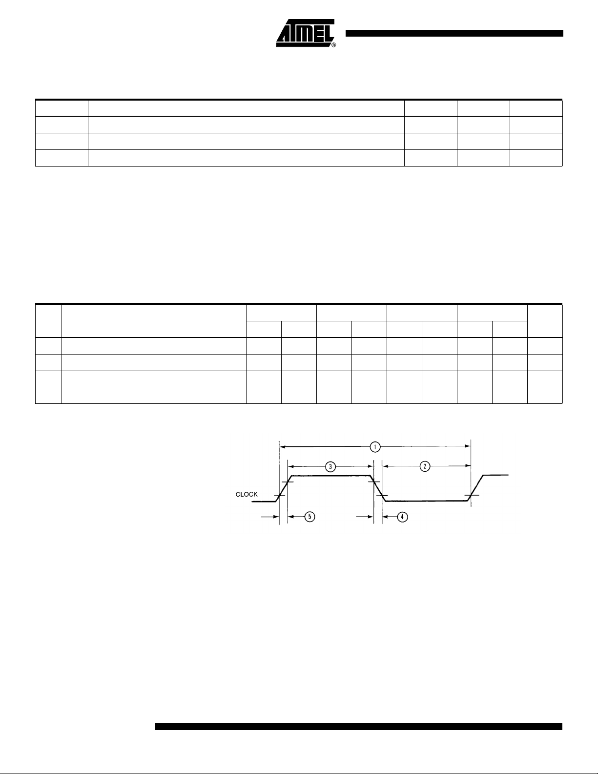
Table 5 . Static Characteristics
=5.0VDC±10%;GND=0VDC;Tc=-55/+125°C or -40/+85°C
V
CC
Symbol Parameter Min Max Unit
I
CC
C
in
C
L
Notes: 1. Test load, see Figure 5.
Dynamic (Switching)
Characteristics
Maximum Supply Current (VCC=5.5V;CLK=f
Capacitance (VIN=0,TA=25°C, f = 1MHz)
Output Load Capacitance 130 pF
2. Capacitance is periodically sampled rather than 100% tested.
; part in Reset) 136 mA
max
(2)
20 pF
The limits and values given in this section apply over the full case temperature range 55°C to +125°C and V
in the range 4.5V to 5.5V, See “AC Electrical Specification Def-
CC
initions” on page 13.
The numbers (N°) refer to the timing diagrams. See Figure 4, Figure 6, Figure 7, Figure
8 and Figure 9.
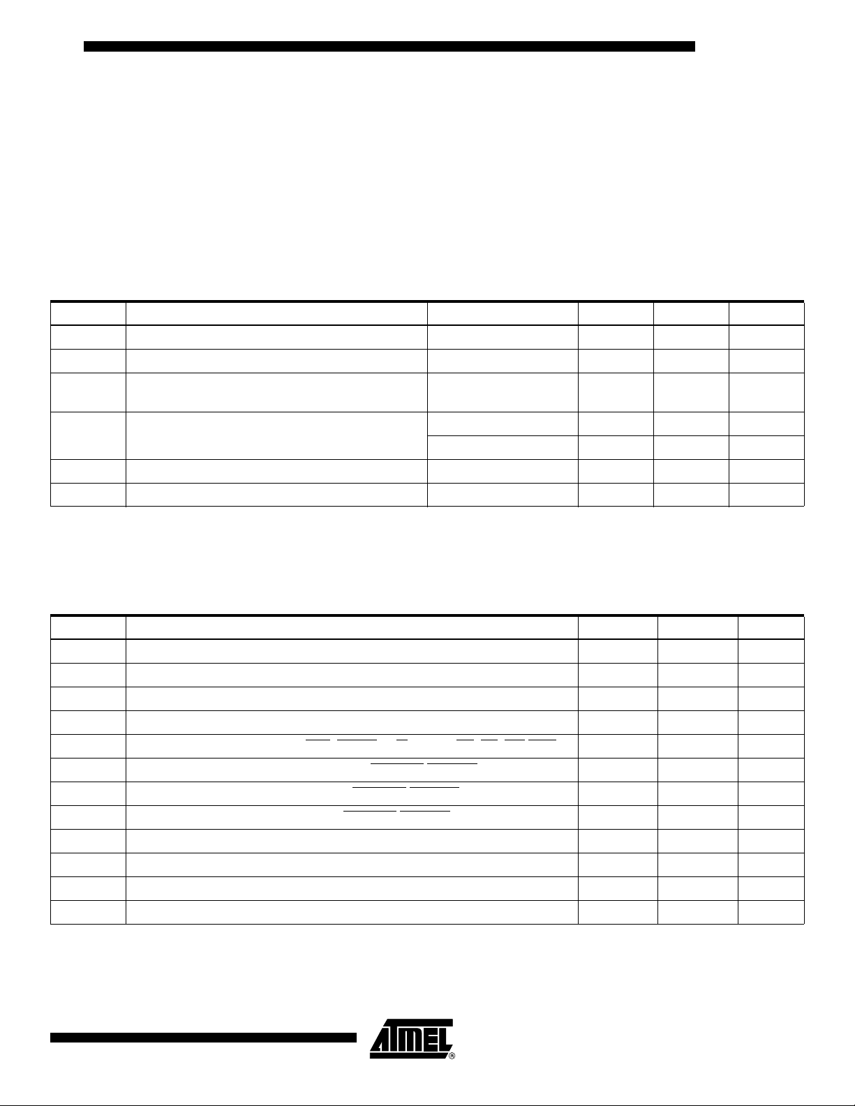
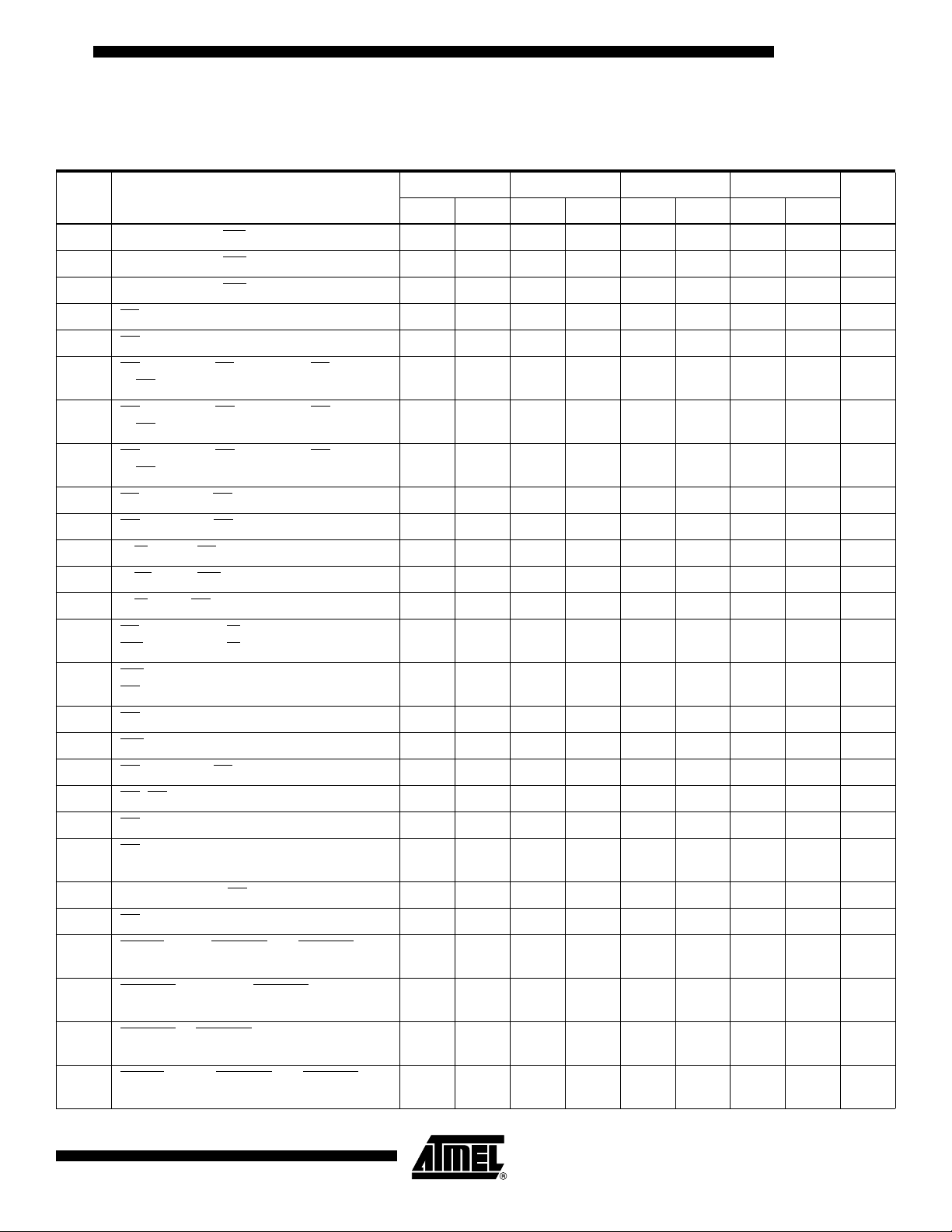
Table 6 . AC Electrical Characteristics - Clock Input
V
=5.0VDC± 10%; GND = 0 V
CC
N° Parameter
Frequency of Operation 8 16.67 12.5 20 12.5 25 16.7 33.33 MHz
1 Clck Time 60 125 50 80 40 80 30 60 ns
2, 3 Clock Pulse Width 24 95 20 54 15 59 14 66 ns
4,5RiseandFallTimes 5543ns
Tc = -55°Cto+125°C(seeFigure4)
DC;
16.67 MHz 20 MHz 25 MHz 33.33 MHz
UnitMin Max Min Max Min Max Min Max
Figure 4. Clock Input Timing Diagram
Note: Timing measurements are referenced to and from a low voltage of 0.8V and a high volt-
age of 2.0V, unless otherwise noted. The voltage swing through this range should start
outside, and pass through, the range such that the rise of fall will be linear between 0.8V
and 2.0V.
10
TS68882
2119A–HIREL–04/02
Page 11
TS68882
Table 7 . AC Electrical Characteristics – Read and Write Cycles
VCC=5.0VDC± 10%; GND = 0 V
N° Parameter
6 Address valid to AS
6a Address valid to DS
6b Address valid to DS
7AS
7a DS
8
8a
8b
9AS
9a DS
10 R/W
10a R/W
10b R/W
negated to address invalid
negated to address invalid
CS
asserted to AS asserted or AS asserted
to CS
asserted
asserted to DS asserted or DS asserted
CS
to CS
asserted (read)
CS
asserted to DS asserted or DS asserted
to CS
asserted (write)
negated to CS negated 10 10 5 5 ns
negated to CS negated 10 10 5 5 ns
high to AS asserted (read) 15 10 5 5 ns
high to DS asserted (read) 15 10 5 5 ns
low to DS asserted(write) 35302525ns
asserted
asserted (read)
asserted (write)
(9)
(9)
(9)
Tc = -55°C/+125°CorTc=-40°C/+85°C (see Figure 7, Figure 8, Figure 9)
DC;
16.67 MHz 20 MHz 25 MHz 33.33 MHz
(5)
(5)
(5)
(6)
(6)
15 10 5 5 ns
15 10 5 5 ns
50 50 35 26 ns
10 10 5 5 ns
10 10 5 5 ns
0000ns
0000ns
30 25 20 15 ns
(1)
UnitMin Max Min Max Min Max Min Max
AS
11
11a
12 DS
13 DS
13a DS
14 CS
15 DS
16
negated to R/W low (read) or
AS
negated to R/W high (write)
negated to R/W low (read) or
DS
DS
negated to R/W high (write)
widthasserted(write) 40383023ns
width negated 40 38 30 23 ns
negated to AS asserted
,DSasserted to data-out valid (read)
negated to data-out invalid (read) 0 0 0 0 ns
DS
negated to data-out high impedance
(read)
17 Data-in invalid to DS
18 DS
19
19a
20
21
negated to data-in invalid (write) 15 10 5 5 ns
START
asserted
DSACK0
(skew)
DSACK0
true to DSACK0 and DSACK1
(2)
asserted to DSACK1 asserted
(7)
or DSACK1 asserted to data-out
valid
START
negated
false to DSACK0 and DSACK1
(8)
10 10 5 5 ns
10 10 5 5 ns
(4)
(2)
30 30 25 18 ns
80 45 45 30 ns
50 35 35 30 ns
asserted(write)15105 5ns
50 35 25 20 ns
-15 15 -10 10 -10 10 5 ns
50 43 32 17 ns
50 30 40 30 ns
2119A–HIREL–04/02
11
Page 12
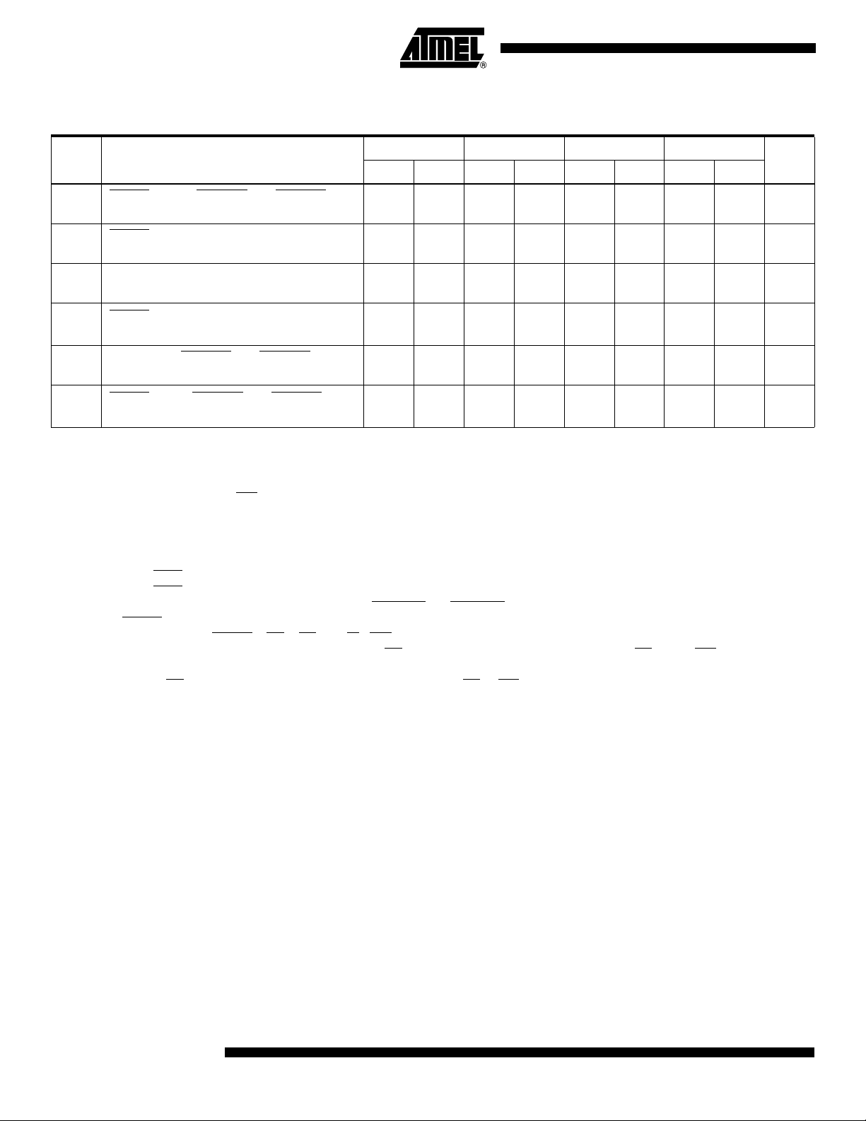
Table 7 . AC Electrical Characteristics – Read and Write Cycles
V
=5.0VDC± 10%; GND = 0 V
CC
Tc = -55°C/+125°CorTc=-40°C/+85°C (see Figure 7, Figure 8, Figure 9)
DC;
16.67 MHz 20 MHz 25 MHz 33.33 MHz
(1)
(Continued)
N° Parameter
START
22
high impedance
START
23
read)
Clock low to data-out valid synchronous
24
read)
START
25
read)
Clock low to DSACK0
26
asserted (synchronous read
START
27
asserted (synchronous read)
false to DSACK0 and DSACK1
true to clock high (synchronous
(3)(8 )
(3)
true to data-out valid (synchronous
(3)(8 )
(8)
and DSACK1
true to DSACK0 and DSACK1
(3)
(3)(8)
70 55 55 40 ns
0000ns
105 80 60 45 ns
0
1.5
105+
2.5
1.5
80 +
2.5
1.5
60+
2.5
1.5
45-
2.5nsClks
75 55 45 30 ns
1.5
75+
2.5
1.5
55+
2.5
1.5
45+
2.5
1.5
30-
2.5nsClks
UnitMin Max Min Max Min Max Min Max
Notes: 1. Timing measurements are referenced to and from a low voltage of 0.8V and a high voltage of 2.0V, unless otherwise noted.
The voltage swing through this range should start outside, and pass through, the range such that the rise or fall will be linear
between 0.8V and 2.0V.
2. These specifications only apply if the TS68882 has completed all internal operations initiated by the termination of the previous bus cycle when DS
was negated.
3. Synchronous read cycles occur only when the save or response CIR locations are read.
4. This specification only applies to systems in which back-to-back accesses (read-write or write-write) of the operand CIR can
occur. When the TS68882 is used as a co-processor to the TS68020/68030, this can occur when the addressing mode is
immediate.
5. If the SIZE
6. If the SIZE
7. This number is reduced to 5 nanoseconds if DSACK0
8. START
this condition is START
9. If a subsequent access is not a FPCP access, CS
pin is not strapped to either VCCor GND, it must have the same setup times as do addresses.
pin is not strapped to either VCCor GND, it must have the same hold times as do addresses.
and DSACK1 have equal loads.
is not an external signal; rather, it is the logical condition that indicates the start of an access. The logical equation for
=CS+AS+(R/W· DS).
must be negated before the assertion of AS and/or DS on the non-FPCP
access. These specifications replace the old specifications 8 and 8A (the old specifications implied that in all cases, transitions in CS
must not occur simultaneously with transitions of AS or DS. This is not a requirement of the TS68882).
12
TS68882
2119A–HIREL–04/02
Page 13
TS68882
Test Conditions Specific
to the Device
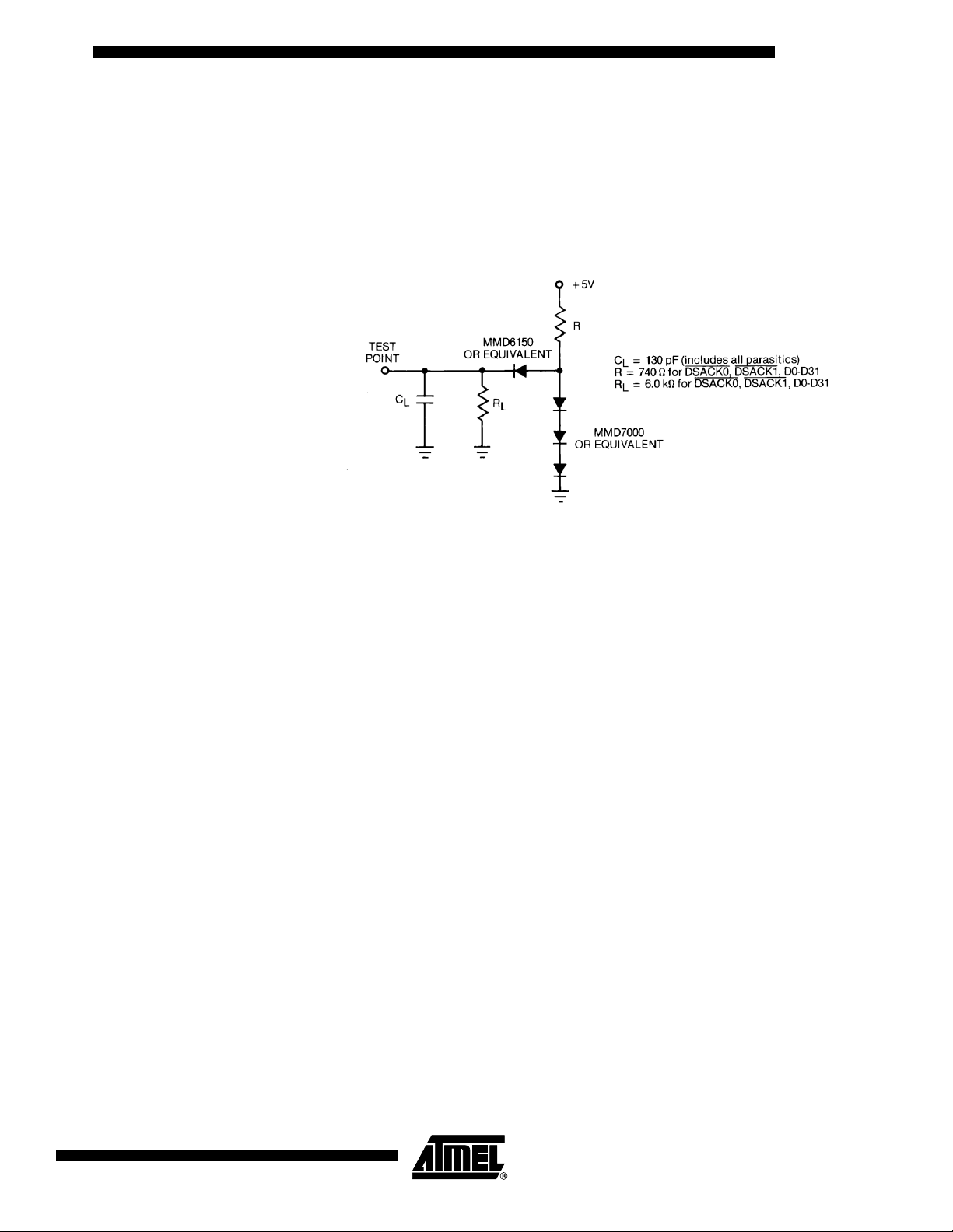
Test Load The applicable loading network shall be as defined in column “Test conditions” of Table
2, referring to the loading network number as shown in Figure 5.
Figure 5. Test Loads
AC Electrical Specification
Definitions
The AC specifications presented consist of output delays, input setup and hold times,
and signal skew times. All signals are specified relative to an appropriate edge of the
clock input and, possibly, relative to one or more other signals.
The measurement of the AC specifications is defined by the waveforms shown in Figure
6. In order to test the parameters guaranteed inputs must be driven to the voltage levels
specified in Figure 6. Outputs are specified with minimum and/or maximum limits, as
appropriate, and are measured as shown. Inputs are specified with minimum and, an
appropriate maximum setup and hold times, and are measured as shown. Finally, the
measurement for signal-to-signal specifications are also shown.
Note that the testing levels used to verify conformance to the AC specifications does not
affect the guaranteed DC operation of the device specified in the DC electrical
characteristics.
2119A–HIREL–04/02
13
Page 14
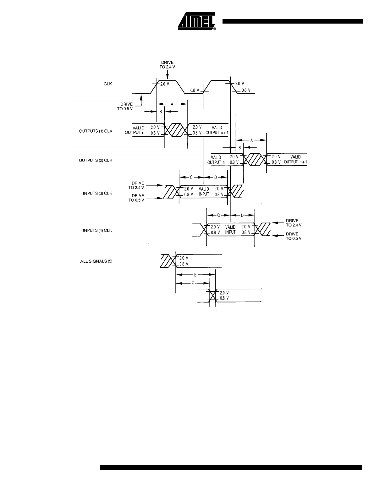
Figure 6. Drive Levels and Test Points for AC Specifications
Legend
A) Maximum output delay specification.
B) Minimum output hold time.
C) Minimum input setup time specification.
D) Minimum input hold time specification.
E) Signal valid to signal valid specification (maximum or minimum).
F) Signal valid to signal invalid specification (maximum or minimum).
Notes: 1. This output timing is applicable to all parameters specified relative to the rising edge of the clock.
2. This output timing is applicable to all parameters specified relative to the falling edge of the clock.
3. This input timing is applicable to all parameters specified relative to the rising edge of the clock.
4. This input timing is applicable to all parameters specified relative to the falling edge of the clock.
5. This timing is applicable to all parameters specified relative to the assertion/negation of another signal.
14
TS68882
2119A–HIREL–04/02
Page 15
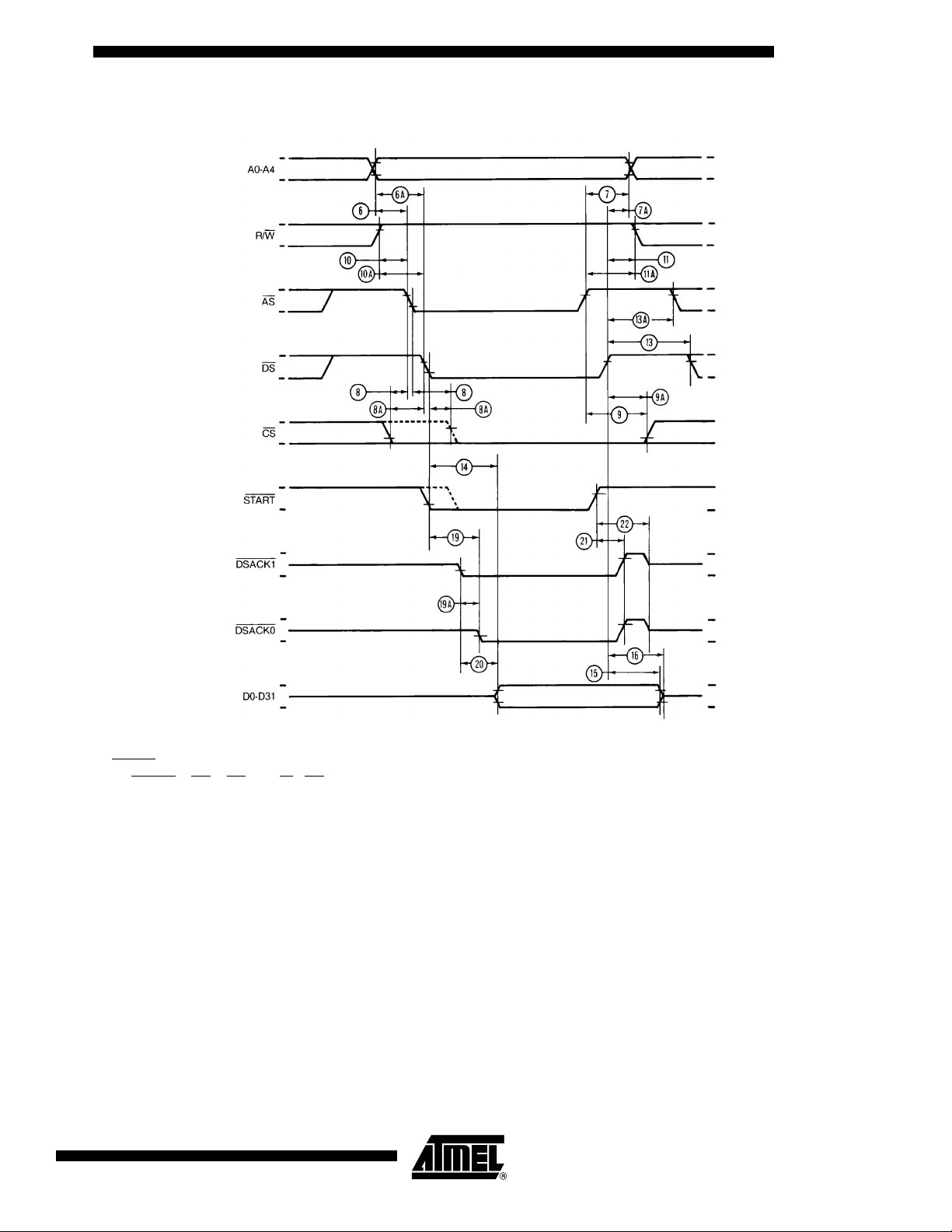
Figure 7. Asynchronous Read Cycle Timing Diagram
TS68882
Note: START is actually a logical condition, but is shown as an active signal for clarity. The logical equation for this signal
is:
START =CS+AS+(R/W· DS).
15
2119A–HIREL–04/02
Page 16

Figure 8. Asynchronous Write Cycle Timing Diagram
Note: START is actually a logical condition, but is shown as an active signal for clarity. The logical equation for this signal is: START =
CS
+AS+(R/W· DS).
16
TS68882
2119A–HIREL–04/02
Page 17

Figure 9. Synchronous Read Cycle Timing Diagram
TS68882
Note: START is actually a logical condition, but is shown as an active signal for clarity. The logical equation for this signal is: START =
CS
+AS+(R/W· DS).
Additional Information Additional information shall not be for any inspection purposes.
Capacitance (Not for Inspection Purposes)
Symbol Parameter Test Conditions Min Max Unit
C
in
2119A–HIREL–04/02
Input Capacitance
Vin=0T
f=1MHz
amb
=25°C
20 pF
17
Page 18

Functional
Description
The Co-processor
Concept
The TS68882 functions as a co-processor in systems where the TS68020 or TS68030 is
the main processor via the TS68000 co-processor interface. It functions as a peripheral
processor in systems where the main processor is the TS68000, TS68010.
The TS68882 utilizes the TS68000 Family co-processor interface to provide extension
of the TS68020 /TS68030 registers and instruction set in a manner which is transparent
to the programmer. The programmer perceives the MPU/FPCP execution model as if
both devices are implemented on one chip.
A fundamental goal of the TS68000 Family co-processor interface is to provide the programmer with an execution model based upon sequential instruction execution by the
TS68020/TS68030 and the TS68882. For optimum performance, however, the co-processor interface allows concurrent operations in the TS68882 with respect to the
TS68020/TS68030 whenever possible. In order to simplify the programmer’s model, the
co-processor interface is designed to emulate, as closely as possible, non-concurrent
operation between the TS68020/TS68030 and the TS68882.
The TS68882 is s non-DMA type co-processor which uses a subset of the general-purpose co-processor interface supported by the TS68020/TS68030. Features of the
interface implemented in the TS68882 are as follows:
• The main processor(s) and TS68882 communicate via standard TS68000 bus
cycles
• The main processor(s) and TS68882 communications are not dependent upon the
instruction sets or internal details of the individual devices (i.e., instruction pipes or
caches, addressing modes)
• The main processor(s) and TS68882 may operate at different clock speeds
• TS68882 instructions utilize all addressing modes provided by the main processor;
all effective addresses are calculated by the main processor at the request of the coprocessor
• All data transfers are performed by the main processor at the request of the
TS68882; thus memory management, bus errors, address errors, and bus
arbitration function as if the TS68882 instructions are executed by the main
processor
• Overlapped (concurrent) instruction execution enhances throughput while
maintaining the programmer’s model of sequential instruction execution
• Co-processor detection of exceptions which require a trap to be taken are serviced
by the main processor at the request of the TS68882 thus exception processing
functions as if the TS68882 instructions were executed by the main processor
• Support of virtual memory/virtual machine systems is provided via the FSAVE and
FRESTORE instructions
• Up to eight co-processors may reside in a system simultaneously: multiple coprocessors of the same type are also allowed
• Systems may use software emulation of the TS68882 without reassembling or
relinking user software
18
TS68882
2119A–HIREL–04/02
Page 19

The TS68882 programming model is shown in Figure 10 through 15, and consists of the
following:
• Eight 80-bit floating-point data registers (FP0-FP7). These registers are analogous
to the integer data registers (D0-D7) and are completely general-purpose (i.e., any
instruction may use any register)
• A 32-bit control register that contains enable bits for each class of exceptions trap,
and mode bits to set the user-selectable rounding and precision modes
• A 32-bit status register that contains floating-point condition codes, quotient bits,
and exception status information
• A 32-bit instruction address register that contains the main processor memory
address of the last floating-point instruction that was executed. This address is used
in exception handling to locate the instruction that caused the exception
The connection between the TS68020/TS68030 and the TS68882 is a simple extension
of the TS68000 bus interface. The TS68882 is connected as a co-processor to the
TS68020/TS68030, and the selection of the TS68882 is based upon a chip select (CS),
which is decoded from the TS68020/TS68030 function codes and address bus. Figure
16 illustrates the TS68882/TS68020 or TS68030 configuration.
Figure 10. TS68882 Programming Model
TS68882
2119A–HIREL–04/02
19
Page 20
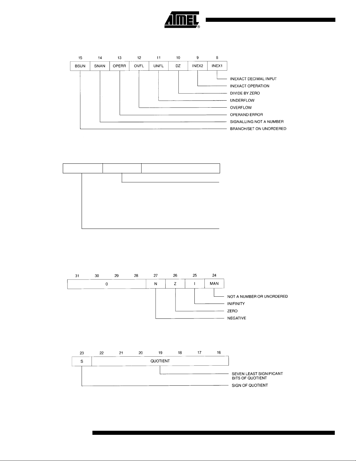
Figure 11. Exception Status/Enable Byte
Figure 12. Mode Control Byte
76
PREC
54 3
RND
2
10
0
ROUNDING MODE:
00 TO NEAREST
01 TOWARD ZERO
10 TOWARD MINUS INFINITY
11 TOWARD PLUS INFINITY
Figure 13. Condition Code Byte
Figure 14. Quotient Byte
ROUNDING PRECISION:
00 extended
01 SINGLE
10 DOUBLE
11 (UNDEFINED RESERVED)
20
TS68882
2119A–HIREL–04/02
Page 21

Figure 15. Accrued Exception Byte
Figure 16. Typical Co-processor Configuration
TS68882
Bus Interface Unit All communications between the TS68020/TS68030 and the TS68882 occur via stan-
dard TS68000 Family bus transfers. The TS68882 is designed to operate on 8-, 16-, or
32-bit data buses.
The TS68882 contains a number of co-processor interface registers (CIRs) which are
addresses in the same manner as memory by the main processor. The TS68000 Family
co-processor interface is implemented via a protocol of reading and writing to these registers by the main processor. The TS68020 and TS68030 implements this generalpurpose co-processor interface protocol in hardware and microcode.
When the TS68020/TS68030 detects a typical TS68882 instruction, the MPU writes the
instruction to the memory-mapped command CIR, and reads the response CIR. In this
response, the BIU encodes requests for any additional action required of the MPU on
behalf of the TS68882. For example, the response may request that the MPU fetch an
operand from the evaluated effective address and transfer the operand to the operated
CIR. Once the MPU fulfills the co-processor request(s), it is free to fetch and execute
subsequent instructions.
21
2119A–HIREL–04/02
Page 22

A key concern in a co-processor interface that allows concurrent instruction execution is
synchronization during main processor and co-processor communication. If a subsequent instruction is written to the TS68882 before the CCU has passed the operands for
the previous instructions to the ECU, the response instructs the TS68020/TS68030 to
wait. Thus, the choice of concurrent or nonconcurrent instruction execution is determined on an instruction-by-instruction basis by the co-processor.
The only difference between a co-processor bus transfer and any other bus transfer is
that the TS68020/TS68030 issues a function code to indicate the CPU address space
during the cycle (the function codes are generated by the TS68000 Family processors to
identify eight separate address spaces). Thus, the memory-mapped co-processor interface registers do not infringe upon instruction or data address spaces. The
TS68020/TS68030 places a co-processor ID field from the co-processor instruction onto
three of the upper address lines during co-processor accesses. This ID, along with the
CPU address space function code, is decoded to select one of eight co-processors in
the system.
Since the co-processor interface protocol is based solely on bus transfers, the protocol
is easily emulated by software when the TS68882 is used as a peripheral with any processor capable of memory-mapped I/O over on TS68000 style bus. When used as a
peripheral processor with the 8-bit TS68008 or the 16-bit TS68000, or TS68010, all
TS68882 instructions are trapped by the main processor to an exception handler at execution time. Thus, the software emulation of the processor interface protocol can be
totally transparent to the user. The system can be quickly upgraded by replacing the
main processor with a TS68020/TS68030 without changes to the user software.
Since the bus is asynchronous, the TS68882 need not run at the same clock speed as
the main processor. Total system performance may therefore be customized. For example, a system requiring very fast floating-point arithmetic with relatively slow integer
arithmetic can be designed with an inexpensive main processor and a fast TS68882.
Co-processor Interface The TS68000 Family co-processor interface is an integral part of the TS68882 and
TS68020/TS68030 designs, with the interface tasks shared between the two. The interface is fully compatible with all present and future TS68000 Family products. Tasks are
partitioned such that the TS68020/TS68030 does not have to decode co-processor
instructions and, the TS68882 does not have to duplicate main processor functions such
as effective address evaluation.
This partitioning provides an orthogonal extension of the instruction set by permitting
TS68882 instructions to utilize all TS68020/TS68030 addressing modes and to generate execution time exception traps. Thus, from the programmer’sview,theCPUandcoprocessor appear to be integrated onto a single chip. While the execution of the majority
of TS68882 instructions may be overlapped with the execution of TS68020/TS68030
instructions, concurrency is completely transparent to the programmer. The
TS68020/TS68030 single-step and program flow (trace) modes are fully supported by
the TS68882 and the TS68000 Family co-processorco-processor interface.
While the TS68000 Family co-processor interface permits co-processors to be bus masters, the TS68882 is never a bus master. The TS68882 requests that the
TS68020/TS68030 fetch all operands and store all results. In this manner, the
TS68020/TS68030 32-bit data bus provides high speed transfer of floating-point operands and results while simplifying the design of the TS68882.
22
TS68882
2119A–HIREL–04/02
Page 23

TS68882
Since the co-processor interface is based solely upon bus cycles and the TS68882 is
never a bus master, the TS68882 can be placed on either the logical or physical side of
the system memory management unit. This provides a great deal of flexibility in the system design.
The virtual machine architecture of the TS68000 Family is supported by the co-processor interface and the TS68882 through the FSAVE and FRESTORE instructions. If the
TS68020/TS68030 detects a page fault and/or task time out, it can force the TS68882 to
stop whatever operation is in process at any time (even in the middle of the execution of
an instruction) and save the TS68882 internal state in memory.
The size of the saved internal state of the TS68882 is dependent upon what the CCU
and ECU are doing at the time that the FSAVE is executed. If the TS68882 is in the
reset state when the FSAVE instruction is received, only one word of state is transferred
to memory, which may be examined by the operating system to determine that the coprocessor programmer’s model is empty. If the co-processor is idle when the save
instruction is received, only a few words of internal state are transferred to memory. If
the TS68882 is in the middle of performing a calculation, it may be necessary to save
the entire internal state of the machine. Instructions that can complete execution in less
time than it would take to save the larger state in mid-instruction are allowed to complete
execution and then save the idle state.
Thus the size of the saved internal state is kept to a minimum. The ability to utilize several internal state sizes greatly reduces the average context switching time.
The FRESTORE instruction permits reloading of an internal state that was saved earlier,
and continue any operation that was previously suspended. Restoring of the reset internal state functions just like a hardware reset to the TS68882 in that defaults are reestablished.
Note: Though the TS68882 is instruction set compatible with the TS68881, the idle and busy
state frames are both 32 bytes larger on the TS68882 than on the TS68881. A unique
format word is generated by the TS68882 so that system software can detect this
difference.
Operand Data Formats The TS68882 supports the following data formats:
• Byte Integer (B)
• Word Integer (W)
• Long Word Integer (L)
• Single Precision Real (S)
• Double Precision Real (D)
• Extended Precision Real (X)
• Packed Decimal String Real (P)
The capital letters contained in parenthesis denote suffixes added to instructions in the
assembly language source to specify the data format to be used.
2119A–HIREL–04/02
23
Page 24

Integer Data Formats The three Integer data formats (byte, word, and long word) are the standard data for-
mats supported in the TS68000 Family architecture. Whenever an integer is used in a
floating-point operation, the integer is automatically converted by the TS68882 to an
extended precision floating-point number before being used. For example, to add an
integer constant of five to the number contained in floating-point data register 3 (FP3),
the following instruction can be used:
FADD.W #5.FP3
The ability to effectively use integers in floating-point operations saves user memory
since an integer representation of a number, if representable, is usually smaller than the
equivalent floating-point representation.
Floating-point Data
Formats
The floating-point data formats single precision (32-bits) and double precision (64-bits)
are as defined by the IEEE standard. These are the main floating-point formats and
should be used for most calculations involving real numbers. Table 8 lists the exponent
and mantissa size for single, double, and extended precision. The exponent is biased,
and the mantissa is in sign and magnitude form. Since single and double precision
require normalized numbers, the most significant bit of the mantissa is implied as one
and is not included, thus giving one extra bit of precision.
Table 8 . Exponent and Mantissa Sizes
Data Format Exponent Bits Mantissa Bits Bias
Single 8 23 (+1) 127
Double 11 52 (+1) 1023
Extended 15 64 16383
The extended precision data format is also in conformance with the IEEE standard, but
the standard does not specify this format to the bit level as it does for single and double
precision. The memory format on the TS68882 consists of 96 bits (three long words).
Only 80 bits are actually used, the other 16 bits are for future expandability and for longword alignment of floating-point data structures. Extended format has a 15-bit exponent,
a 64-bit mantissa, and a 1-bit mantissa sign.
Extended precision numbers are intended for use as temporary variables, intermediate
values, or in places where extra precision is needed. For example, a compiler might
select extended precision arithmetic for evaluation of the right side of an equation with
mixed sized data and then convert the answer to the data type on the left side of the
equation. It is anticipated that extended precision data will not be stored in large arrays,
due to the amount of memory required by each number.
24
TS68882
2119A–HIREL–04/02
Page 25

TS68882
Packed Decimal String
Real Data Format
The packed decimal string data format allows packed BCD strings to be input to and
output from the TS68882. The strings consist of a 3-digit base 10 exponent and a 17digit base 10 mantissa. Both the exponent and mantissa have a separate sign bit. All
digits are packed BCD, such that an entire string fits in 96 bits (three long words). As is
the case with all data formats, when packed BCD strings are input to the TS68882, the
strings are automatically converted to extended precision real values. This allows
packed BCD numbers to be used as inputs to any operation. For example:
FADD.P # - 6.023E + 24, FP5
BCD numbers can be output from the TS68882 in a format readily used for printing by a
program generated by a high-level language compiler. For example:
FMOVE.P FP3.BUFFER (# -5)
instructs the TS68882 to convert the floating-point data register 3 (FP3) contents into a
packed BCD string with five digits to the right of the decimal point (FORTRAN F format).
Data Format Summary All data formats described above are supported orthogonally by all arithmetic and tran-
scendental operations, and by all appropriate TS68000 Family addressing modes. For
example, all of the following are legal instructions:
FADD.B # 3.FP0
FADD.W D2.FP3
FADD.L BIGINT.FP7
FADD.S # 3.14159.FP5
FADD.D (SP) + .FP6
FADD.X [(TEMP -PTR.A7)].FP3
FADD.P # 1.23E25.FP0
On-chip calculations are performed to extended precision format, and the eight floatingpoint data registers always contain extended precision values. All data used in an operation is converted to extended precision by the TS68882 before the specific operation is
performed, and all results are in extended precision. This ensures accuracy without sacrificing performance.
Refer to Figure 17 for a summary of the memory formats for the seven data formats supported by the TS68882.
2119A–HIREL–04/02
25
Page 26

Figure 17. TS68882 Data Format Summary
Instruction Set The TS68882 instruction set is organized into six major classes:
1. Moves Between The TS68882 and Memory or The MPU (In and Out)
2. Move Multiple Registers (In and Out)
3. Monadic Operations
4. Dyadic Operations
5. Branch, Set, or Trap Conditionally, and
6. Miscellaneous
Moves All moves from memory (or from an MPU data register) to the TS68882, cause data con-
version from the source data format to the internal extended precision format.
All moves from the TS68882 to memory (or to an MPU data register), cause data conversion from the internal extended precision format to the destination data format.
26
TS68882
2119A–HIREL–04/02
Page 27

TS68882
Note that data movement instructions perform arithmetic operations, since the result is
always rounded to the precision selected in the FPCR mode control byte. The result is
rounded using the selected rounding mode, and is checked for overflow and underflow.
Thesyntaxforthemoveis:
FMOVE.(fmt) (ea).FPn Move to TS68882
FMOVE.(fmt) FPm.(ea) Move from TS68882
FMOVE.X FPm.FPn Move within TS68882
where:
(ea) is a TS68000 Family effective address operand and (fmt) is the data format size.
FPm and FPn are floating-point data registers.
Move Multiples The floating-point move multiple instructions on the TS68882 are much like the integer
counterparts on the TS68000 Family processors. Any set of the floating-point registers
FP0 through FP7 can be moved to or from memory with one instruction. These registers
are always moved as 96-bit extended data with no conversion (hence no possibility of
conversion errors). Some move multiple examples are as follows:
FMOVEM (ea), FP0-FP3/FP7
FMOVEM FP2/FP4/FP6,(ea)
Move multiples are useful during context switches and interrupts to save or restore the
state of a program. These moves are also useful at the start and end of a procedure to
save and restore the calling routine’s register set. In order to reduce procedure call overhead, the list of registers to be saved or restored can be contained in a data register.
This allows run-time optimization by allowing a called routine to save as few registers as
possible. Note that no rounding or overflow/underflow checking is performed by these
operations.
Monadic Operations Monadic operations have one operand. This operand may be in a floating-point data
register, memory, or in an MPU data register. The result is always stored in a floatingpoint data register. For example, the syntax for square root is:
FSQRT.(fmt) (ea), FPN or,
FSQRT.X FPm, FPn or,
FSQRT.X FPn
The TS68882 monadic operations available are as follows:
FABS Absolute Value
FACOS Arc Cosine
FASIN Arc Sine
2119A–HIREL–04/02
FATAN Arc Tangent
FATANH Hyperbolic Arc Tangent
FCOS Cosine
FCOSH Hyperbolic Cosine
FETOX e to the x Power
27
Page 28

FABS Absolute Value
FACOS Arc Cosine
FETOXM1 e to the x Power - 1
FGETEXP Get Exponent
FGETMAN Get Mantissa
FINT Integer Part
FINTRZ Integer Part (Truncated)
FLOG10 Log Base 10
FLOG2 Log Base 2
FLOGN Log Base e
FLOGNP Log Base e of(x + 1)
FNEG Negate
FSIN Sine
FSINCOS Simultaneous Sine and Cosine
FSINH Hyperbolic Sine
FSQRT Square Root
FTAN Tangent
FTANH Hyperbolic Tangent
FTENTOX 10 to the x Power
FTST test
FTWOTOX 2 to the x Power
Dyadic Operations Dyadic operations have two input operands. The first input operand comes from a float-
ing-point data register, memory, or MPU data register. The second input operand comes
from a floating-point data register. The destination is the same floating-point data register used for the second input. For example, the syntax for add is:
FADD.(fmt) (ea).FPnor,
FADD.X FPm.FPn
The TS68882 dyadic operations available are as follows:
FADD Add
FCMP Compare
FDIV Divide
FMOD Modulo Remainder
FMUL Multiply
FREM IEEE Remainder
FSCALE Scale Exponent
28
TS68882
2119A–HIREL–04/02
Page 29

FADD Add
FSGLDIV Single Precision Divide
FSGLMUL Single Precision Multiply
FSUB Subtract
TS68882
Branch, Set, and Trap-on
Condition
The floating-point branch, set, and trap-on condition instructions implemented by the
TS68882 are similar to the equivalent integer instructions of the TS68000 Family processors, except that more conditions exist due to the special values in IEEE floatingpoint arithmetic. When a conditional instruction is executed, the TS68882 performs the
necessary condition checking and tells the MPU whether the condition is true or false;
the MPU then takes the appropriate action. Since the TS68882 and TS68020/TS68030
are closely coupled, the floating-point branch operations executed by the pair are very
fast.
The TS68882 conditional operations are:
FBcc Branch
FDBcc Decrement and Branch
FScc Set Byte According to Condition
FTRAPcc
Trap-on Condition (with an Optional
Param eter)
where:
cc is one of the 32 floating-point conditional test specifiers as shown in Table 9.
rs
Table 9 . Floating-point Conditional Test Specifiers
Mnemonic Definition
Note: The following conditional tests do not set the BSUN bit in the status register exception byte under any circumstances.
FFalse
EQ Equal
OGT Ordered Greater Than
OGE Ordered Greater Than or Equal
OLT Ordered Less Than
OLE Ordered Less Than or Equal
OGL Ordered Greater or Less Than
OR Ordered
UN Unordered
UEQ Unordered or Equal
UGT Unordered or Greater Than
UGE Unordered or Greater or Equal
ULT Unordered or Less Than
ULE Unordered or Less or Equal
NE Not Equal
2119A–HIREL–04/02
29
Page 30

Table 9 . Floating-point Conditional Test Specifiers (Continued)
Mnemonic Definition
TTrue
Note: The following conditional tests set the BSUN bit in the status register exception byte if the NAN condition code bit is set when a
conditional instruction is executed.
SF Signaling False
SEQ Signaling Equal
GT Greater Than
GE Greater Than or Equal
LT Less Than
LE Less Than or Equal
GL Greater or Less Than
GLE Greater Less or Equal
NGLE Not (Greater, Less or Equal)
NGL Not (Greater or Less)
NLE Not (Less or Equal)
NLT Not (Less Than)
NGE Not (Greater or Equal)
NGT Not (Greater Than)
SNE Signaling Not Equal
ST Signaling True
Miscellaneous
Instructions
Miscellaneous instructions include moves to and from the status, control, and instruction
addressregistersandanooperationfunctionthatcanbeusedto“flush” exceptions.
Also included are the virtual memory/machine FSAVE and FRESTORE instructions that
save and restore the internal state of the TS68882.
FMOVE (ea),FPcr Move to Control Register(s)
FMOVE FPcr,(ea) Move from Control Register(s)
FNOP No Operation
FSAVE (ea) Virtual Machine State Save
FRESTORE (ea) Virtual Machine State Restore
Addressing Modes The TS68882 does not perform address calculations. This satisfies the criterion that a
TS68000 Family co-processor must not depend on certain features or capabilities that
may or may not be implemented by a given main processor. Thus, when the TS68882
instructs the TS68020/TS68030 to transfer an operand via the co-processor interface,
the MPU performs the addressing mode calculations requested in the instruction. In this
case, the instruction is encoded specifically for the TS68020/TS68030, and the execution of the TS68882 is not dependent on that encoding, but only on the value of the
command word written to the TS68882 by the main processor.
30
TS68882
2119A–HIREL–04/02
Page 31

TS68882
This interface is quite flexible and allows any addressing mode to be used with floatingpoint instructions. For the TS68000 Family, these addressing modes include immediate,
postincrement, predecrement, data or address register direct, and the indexed/indirect
addressing modes of the TS68020/TS68030. Some addressing modes are restricted for
some instructions in keeping with the TS68000 Family architectural definitions (i.e., PC
relative addressing is not allowed for a destination operand).
The orthogonal instruction set of the TS68882, along with the flexible branches and
addressing modes, allows a programmer writing assembly language code, or a compiler
writer generating object or source code for the MPU/TS68882 device pair, to think of the
TS68882 as though it is part of the MPU. There are no special restrictions imposed by
the co-processor interface, and floating-point arithmetic is coded exactly like integer
arithmetic.
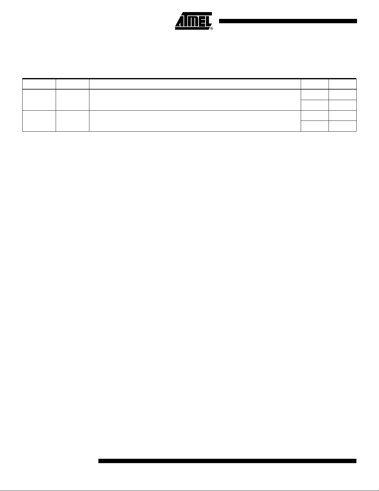
Address Bus (A0 through
A4)
These active-high address line inputs are used by the main processor to select the coprocessor interface register locations located in the CPU address space. These lines
control the register selection as listed in Table 10.
When the TS68882 is configured to operate over an 8-bit data bus, the A0 pin is used as
an address signal for byte accesses of the co-processor interface registers. When the
TS68882 is configured to operate over a 16- or 32-bit system data bus, both the A0 and
SIZE pins are strapped high and/or low as listed in Table 11.
Table 10. Co-processor Interface Register Selection
A4-A0 Offset Width Type Register
0000x S00 16 Read Response
0001x S02 16 Write Control
0010x S04 16 Read Save
0011x S06 16 R/W Restore
0100x S08 16 - (Reserved)
0101x S0A 16 Write Command
0110x S0C 16 - (Reserved)
0111x S0E 16 Write Condition
100xx S10 32 R/W Operand
2119A–HIREL–04/02
1010x S14 16 Read Register select
1011x S16 16 - (Reserved)
110xx S18 32 Read Instruction Address
111xx S1C 32 R/W Operand Address
Table 11. System Data Bus Size Configuration
A0 Size Data bus
Low 8-bit
Low High 16-bit
High High 32-bit
31
Page 32

Data Bus (D0 through
D31)
This 32-bit, bi-directional, three-state bus serves as the general-purpose data path
between the TS68020/TS68030 and the TS68882. Regardless of whether the TS68882
is operated as a co-processor or a peripheral processor, all inter-processor transfers of
instruction information, operand data, status information, and requests for service occur
as standard TS68000 bus cycles.
The TS68882 will operate over an 8-, 16-, or 32-bit system data bus. Depending upon
the system data bus configuration, both the A0 and SIZE
for the applicable bus configuration. (Refer to ADDRESS BUS (A0 through A4) and
SIZE (SIZE
for further details).
pins are configured specifically
Size (SIZE) This active-low input signal is used in conjunction with the A0 pin to configure the
TS68882 for operation over an 8-, 16-, or 32-bit system data bus. When the TS68882 is
configured to operate over a 16-or 32-bit system data bus, both the SIZE
are strapped high and/or low as listed in Table 11.
and A0 pins
Address Strobe (AS) This active-low input signal indicates that there is a valid address on the address bus,
and both the chip select (CS)
and read/write (R/W signal lines are valid).
Chip Select (CS) This active-low input signal enables the main processor access to the TS68882 co-pro-
cessor interface registers. When operating the TS68882 as a peripheral processor, the
chip select decode is system dependent (i.e., like the chip select on any peripheral). The
CS
signal must be valid (either asserted or negated) when AS is asserted. Refer to
CHIP SELECT TIMING for further discussion of timing restrictions for this signal.
Read/Write (R/W) This input signal indicates the direction of a bus transaction (read/write) by the main pro-
cessor. A logic high (1) indicates a read from the TS68882, and a logic low (0) indicates
a write to the TS68882. The R/W
signal must be valid when AS is asserted.
Data Strobe (DS) This active-low input signal indicates that there is valid data on the data bus during a
write bus cycle.
Data Transfer and Size
Acknowledge (DSACK0
DSACK1
)
,
These active-low, three-state output signals indicate the completion of a bus cycle to the
main processor. The TS68882 asserts both the DSACK0
assertion of CS
If the bus cycle is a main processor read, the TS68882 asserts DSACK0
signals to indicate that the information on the data bus is valid. (Both DSACK signals
may be asserted in advance of the valid data being placed on the bus). If the bus cycle
is a main processor write to the TS68882, DSACK0
edge acceptance of the data by the TS68882.
TheTS68882alsousesDSACK0
TS68020/TS68030 the “port” size (system data bus width) on a cycle-by-cycle basis.
Depending upon which of the two DSACK pins are asserted in a given bus cycle, the
TS68020/TS68030 assumes data has been transferred to/from an 8-, 16-, or 32-bit wide
data port. Table 12 lists the DSACK assertions that are used by the TS68882 for the
various bus cycles over the various bus cycles over the various system data bus
configurations.
.
and DSACK1 signals to dynamically indicate to the
,andDSACK1signals upon
and DSACK1
and DSACK1 are used to acknowl-
32
TS68882
2119A–HIREL–04/02
Page 33

TS68882
Table 12 indicates that all accesses over a 32-bit bus where A4 equals zero are to 16-bit
registers. The TS68882 implements all 16-bit co-processor interface registers on data
lines D16 - D13 (to eliminate the need for on-chip multiplexers); however, the
TS68020/TS68030 expects 16-bit registers that are located in a 32-bit port at odd word
addresses (A1 = 1) to be implemented on data lines D0-D15. For accesses to these registers when configured for 32-bit bus operation, the TS68882 generates DSACK signals
as listed in Table 12 to inform the TS68020/TS68030 of valid data on D16 - D31 instead
of D0-D15.
An external holding resistor is required to maintain both DSACK0
between bus cycles. In order to reduce the signal rise time, the DSACK0
lines are actively pulled up (negated) by the TS68882 following the rising edge of AS or
DS
and both DSACK lines are then three-stated (placed in the high-impedance state) to
avoid interference with the next bus cycle.
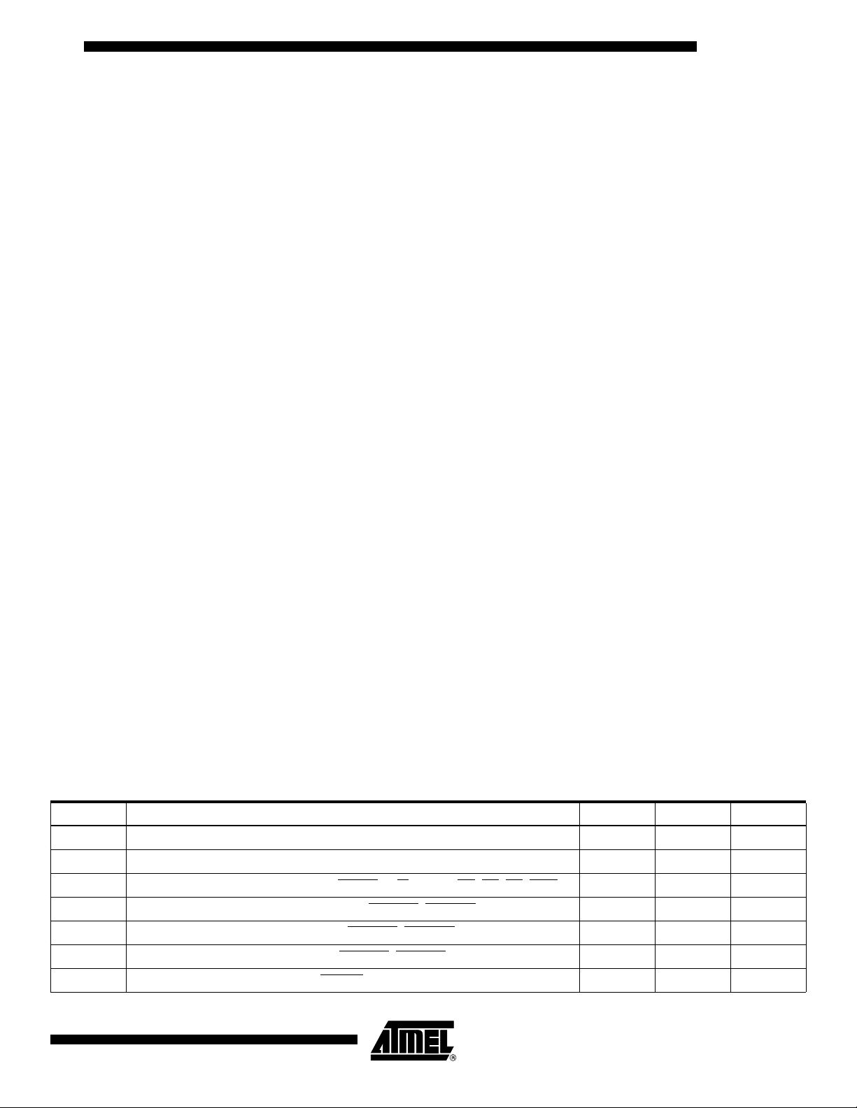
Table 1 2 . DSACK Assertions
Data Bus A4 DSACK1 DSACK2 Comments
32-bit 1 L L Valid data on D31-D0
32-bit 0 L H Valid data on D31-D16
16-bit x L H Valid data on D31-D16 or D15-D0
8-bit x H L Valid data on D31-D24, D23-D16, D15-D8, D7-D0
All x H H Insert Wait States in Current Bus Cycle
Reset (RESET)
This active-low input signal causes the TS68882 to initialize the floating-point data registers to non-signaling not-a-numbers (NANs) and clears the floating-point control, status,
and instruction address registers.
When performing a power-up reset, external circuitry should keep the RESET
asserted to a minimum of four clock cycles after V
CC
correct initialization of the TS68882 when power is applied. For compatibility with all
TS68000 Family devices, 100 milliseconds should be used as the minimum.
and DSACK1 high
and DSACK1
line
is within tolerance. This assures
When performing a reset of the TS68882 after V
than the initial power-up time, the RESET
line must have an asserted pulse width which
has been within tolerance for more
CC
is greater than two clock cycles. For compatibility with all TS68000 Family devices, 10
clock cycles should be used as the minimum.
Clock (CLK) The TS68882 clock input is a TTL-compatible signal that is internally buffered for devel-
opment of the internal clock signals. The clock input should be a constant frequency
square wave with no stretching or shaping techniques required. The clock should not be
gated off at any time and must conform to minimum and maximum period and pulse
width times.
Sense Device (SENSE
) This pin may be used optionally as an additional GND pin, or as an indicator to external
hardware that the TS68882 is present in the system. This signal is internally connected
to the GND of the die, but it is not necessary to connect it to the external ground for correct device operation. If a pullup resistor (which should be larger than 10 kΩ)is
connected to this pin location, external hardware may sense the presence of the
TS688882 in a system.
33
2119A–HIREL–04/02
Page 34

Power (VCCand GND) These pins provide the supply voltage and system reference level for the internal cir-
cuitry of the TS68882. Care should be taken to reduce the noise level on these pins with
appropriate capacitance decoupling.
No Connect (NC) One pin of the TS68882 package is designated as a no connect (NC). This pin position
is reserved for future use, and should not be used for signal routing or connected to V
or GND.
Interfacing Methods TS68882/TS68020 or TS68030 interfacing
The following paragraphs describe how to connect the TS68882 to a TS68020 or
TS68030 for co-processor operation via an 8-, 16-, or 32-bit data bus.
CC
32-bit Data Bus Co-processor
Connection
16-bit Data Bus Co-processor
Connection
8-bit Data Bus Co-processor
Connection
Figure 18 illustrates the co-processor interface connection of a TS68882 to a
TS68020/TS68030 via a 32-bit data bus. The TS68882 is configured to operate over a
32-bit data bus when both the A0 and SIZE
Figure 19 illustrates the co-processor interface connection of a TS68882 to a
TS68020/TS68030 via a 16-bit data bus. The TS68882 is configured to operate over a
16-bit data bus when the SIZE
GND. The sixteen least significant data pins (D0-D15) must be connected to the sixteen
most significant data pins (D16 - D31) when the TS68882 is configured to operate over
a 16-bit data bus (i.e., connect D0 to D16, D1 to D17,... and D15 to D31). The DSACK
pins of the two devices are directly connected, although it is not necessary to connect
the DSACK0
Figure 20 illustrates the connection of a TS68882 to a TS68020/TS68030 as a co-processor over an 8-bit data bus. The TS68882 is configured to operate over an 8-bit data
bus when the SIZE
(D0-D23) must be connected to eight most significant data pins (D24-D31) when the
TS68882 is configured to operate over an 8-bit data bus (i.e., connect D0 to D8, D16 to
D24; D1 to D9, D17, and D15;... and D7 to D15, D23 and D31). The DSACK pins of the
two devices are directly connected, although it is not necessary to connect the DSACK1
pin since the TS68882 never asserts it in this configuration.
TS68882/TS68000/TS68008/TS68010 Interfacing
•
The following paragraphs describe how to connect the TS68882 to a TS68000,
TS68008, or TS68010 processor for operation as a peripheral via an 8- or 16-bit data
bus.
pin since the TS68882 never asserts it in this configuration.
pin is connected to GND. The twenty four least significant data pins
pin is connected to VCC, and the A0 pin is connected to
pins are connected to VCC.
16-bit Data Peripheral
Processor Connection
34
TS68882
Figure 21 illustrates the connection of a TS68882 to a TS68000 or TS68010 as a peripheral processor over an 16-bit data bus. The TS68882 is configured to operate over an
16-bit data bus when the SIZE
GND. The sixteen least significant data pins (D0-D15) must be connected to the sixteen
most significant data pins (D16 - D31) when the TS68882 is configured to operate over
an 16-bit data bus (i.e., connect D0 to D16, D1 to D17,... and D15 to D31). The DSACK1
pin of the TS68882, is connected to the DTACK pin of the main processor, and the
DSACK0
pin is not used.
pin is connected to VCC, and the A0 pin is connected to
2119A–HIREL–04/02
Page 35

TS68882
When connected as a peripheral processor, the TS68882 chip select (CS)decodeis
system dependent. If the TS68000 is used as the main processor, the TS68882 CS
must be decoded in the supervisor or user data spaces. However, if the TS68010 is
used as the main processor, the MOVES instruction may be used to emulate any CPU
space access that the TS68020/co-processorTS68030 generates for co-processor communications. Thus, the CS
TS68020/TS68030 systems, such that the TS68882 will not use any part of the data
address spaces.
Figure 18. 32-bit Data Bus co-processor Connection
decode logic for such systems may be the same as in a
2119A–HIREL–04/02
35
Page 36

Figure 19. 16-bit Data Bus co-processor Connection
GND
Figure 20. 8-bit Data Bus Co-processor Connection
GND
36
TS68882
2119A–HIREL–04/02
Page 37

Figure 21. 16-bit Data Bus Peripheral Processor Connection
TS68882
Figure 22. 8-bit Data Bus Peripheral Processor Connection
2119A–HIREL–04/02
37
Page 38

8-bit Data Bus Peripheral
Processor Connection
Figure 22 illustrates the connection of a TS68882 to a TS68008 as a peripheral processor over an 8-bit data bus. The TS68882 is configured to operate over an 8-bit data bus
when the SIZE
must be connected to the twenty four most significant data pins (D8-D31) when the
TS68882 is configured to operate over an 8-bit data bus (i.e., connect D0 to D8, D16
and D24; D1 to D9, D17, and D25;... and D7 to D 15, D 23, and D31). The DSACK0
of the TS68882 is connected to the DTACK
not used.
pin is connected to GND. The eight least significant data pins (D0-D7)
pin
pin of the TS68008, and the DSACK1 pin is
When connected as a peripheral processor, the TS68882 chip select (CS
system dependent, and the CS
must be decoded in the supervisor or user data spaces.
)decodeis
Preparation For
Delivery
Certificate of
Compliance
ATMEL-Grenoble offers a certificate of compliance with each shipment of parts, affirming the products are in compliance with MIL-STD-883 and guaranteeing the parameters
are tested at extreme temperatures for the entire temperature range.
Handling Devices must be handled with certain precautions to avoid damage due to accumulation
of static charge. Input protection devices have been designed in the chip to minimize the
effect of this static buildup. However, the following handling practices are
recommended:
a) Device should be handled on benches with conductive and grounded surface.
b) Ground test equipment, tools and operator.
c) Do not handle devices by the leads.
d) Store devices in conductive foam or carriers.
e) Avoid use of plastic, rubber, or silk.
f) Maintain relative humidity above 50%, if practical.
38
TS68882
2119A–HIREL–04/02
Page 39

Package Mechanical
Data
Figure 23. 68-lead CPGA
TS68882
Notes: 1. Dimensions A and B are datums and T S datum surface.
2. Positional tolerance for leads 168 places:
θφ0.13 0.005()T, A (5)|B (5)
3. Dimensioning and tolerancing per AN5I Y14 5M 1982.
4. Controlling dimension: INCH.
2119A–HIREL–04/02
39
Page 40

Figure 24. 68-lead CQFP
40
TS68882
2119A–HIREL–04/02
Page 41

Ordering Information
HI-REL Product
TS68882
Commercial Atmel
Part-Number Norms Package
TS68882MRB/C16 MIL-STD-883 PGA 68 -55 / +125 16.67 -
TS68882MRB/C20 MIL-STD-883 PGA 68 -55 / +125 20 -
TS68882MRB/C25 MIL-STD-883 PGA 68 -55 / +125 25 -
TS68882MRB/C33 MIL-STD-883 PGA 68 -55 / +125 33 -
TS68882MFB/C16 MIL-STD-883 CQFP 68 -55 / +125 16.67 -
TS68882MFB/C20 MIL-STD-883 CQFP 68 -55 / +125 20 -
TS68882MFB/C25 MIL-STD-883 CQFP 68 -55 / +125 25 -
TS68882DESC01XA DESC PGA 68 -55 / +125 16.67 5962 8946301XA
TS68882DESC02XA DESC PGA 68 -55 / +125 20 5962 8946301XA
TS68882DESC03XA DESC PGA 68 -55 / +125 25 5962 8946301XA
TS68882DESC04XA DESC PGA 68 -55 / +125 33 5962 8946301XA
TS68882DESC01YA DESC CQFP 68 -55 / +125 16.67 5962 8946301XA
TS68882DESC02YA DESC CQFP 68 -55 / +125 20 5962 8946301XA
TS68882DESC03YA DESC CQFP 68 -55 / +125 25 5962 8946301XA
TS68882DESC04YA DESC CQFP 68 -55 / +125 33 5962 8946304YA
Temperature Range
Tc (°C)
Frequency
(MHz) Drawing Number
Standard Product
Commercial Atmel
Part-Number Norms Package
TS68882VR16 ATMEL-Grenoble Standard PGA 68 -40 / +85 16.67 Internal
TS68882VR20 ATMEL-Grenoble Standard PGA 68 -40 / +85 20 Internal
TS68882VR25 ATMEL-Grenoble Standard PGA 68 -40 / +85 25 Internal
TS68882VR33 ATMEL-Grenoble Standard PGA 68 -40 / +85 33 Internal
TS68882MR16 ATMEL-Grenoble Standard PGA 68 -55 / +125 16.67 Internal
TS68882MR20 ATMEL-Grenoble Standard PGA 68 -55 / +125 20 Internal
TS68882MR25 ATMEL-Grenoble Standard PGA 68 -55 / +125 25 Internal
TS68882MR33 ATMEL-Grenoble Standard PGA 68 -55 / +125 33 Internal
TS68882VF16 ATMEL-Grenoble Standard CQFP 68 -40 / +85 16.67 Internal
TS68882VF20 ATMEL-Grenoble Standard CQFP 68 -40 / +85 20 Internal
TS68882VF25 ATMEL-Grenoble Standard CQFP 68 -40 / +85 25 Internal
TS68882VF33 ATMEL-Grenoble Standard CQFP 68 -40 / +85 33 Internal
TS68882MF16 ATMEL-Grenoble Standard CQFP 68 -55 / +125 16.67 Internal
Temperature Range
Tc (°c)
Frequency
MHZ Drawing Number
2119A–HIREL–04/02
41
Page 42

Standard Product
Commercial Atmel
Part-Number Norms Package
Temperature Range
Tc (°c)
Frequency
MHZ Drawing Number
TS68882MF20 ATMEL-Grenoble Standard CQFP 68 -55 / +125 20 Internal
TS68882MF25 ATMEL-Grenoble Standard CQFP 68 -55 / +125 25 Internal
TS68882MF33 ATMEL-Grenoble Standard CQFP 68 -55 / +125 33 Internal
TS68882
Type
Temperature range: Tc
M: -55/+125°C
V: -40/+85°C
Package
R = Pin grid array 68
F = CQFP 68
M R
B/C
20
Speed (MHz)
Screening
- = Standard
B/C = MIL STD 883 Class B
1
Note: For availability of the different versions, contact your Atmel sales office.
Hirel lead finish
1: Hot solder dip (883C)
Gold
42
TS68882
2119A–HIREL–04/02
Page 43

Atmel Headquarters Atmel Operations
Corporate Headquarters
2325 Orchard Parkway
San Jose, CA 95131
TEL 1(408) 441-0311
FAX 1(408) 487-2600
Europe
Atmel Sarl
Route des Arsenaux 41
Case Postale 80
CH-1705 Fribourg
Switzerland
TEL (41) 26-426-5555
FAX (41) 26-426-5500
Asia
Atmel Asia, Ltd.
Room 1219
Chinachem Golden Plaza
77 Mody Road Tsimhatsui
East Kowloon
Hong Kong
TEL (852) 2721-9778
FAX (852) 2722-1369
Japan
Atmel Japan K.K.
9F, Tonetsu Shinkawa Bldg.
1-24-8 Shinkawa
Chuo-ku, Tokyo 104-0033
Japan
TEL (81) 3-3523-3551
FAX (81) 3-3523-7581
Memory
Atmel Corporate
2325 Orchard Parkway
San Jose, CA 95131
TEL 1(408) 441-0311
FAX 1(408) 436-4314
Microcontrollers
Atmel Corporate
2325 Orchard Parkway
San Jose, CA 95131
TEL 1(408) 441-0311
FAX 1(408) 436-4314
Atmel Nantes
La Chantrerie
BP 70602
44306 Nantes Cedex 3, France
TEL (33) 2-40-18-18-18
FAX (33) 2-40-18-19-60
ASIC/ASSP/Smart Cards
Atmel Rousset
Zone Industrielle
13106 Rousset Cedex, France
TEL (33) 4-42-53-60-00
FAX (33) 4-42-53-60-01
Atmel Colorado Springs
1150 East Cheyenne Mtn. Blvd.
Colorado Springs, CO 80906
TEL 1(719) 576-3300
FAX 1(719) 540-1759
RF/Automotive
Atmel Heilbronn
Theresienstrasse 2
Postfach 3535
74025 Heilbronn, Germany
TEL (49) 71-31-67-0
FAX (49) 71-31-67-2340
Atmel Colorado Springs
1150 East Cheyenne Mtn. Blvd.
Colorado Springs, CO 80906
TEL 1(719) 576-3300
FAX 1(719) 540-1759
Biometrics/Imaging/Hi-Rel MPU/
High Speed Converters/RF Datacom
Atmel Grenoble
Avenue de Rochepleine
BP 123
38521 Saint-Egreve Cedex, France
TEL (33) 4-76-58-30-00
FAX (33) 4-76-58-34-80
Atmel Smart Card ICs
Scottish Enterprise Technology Park
Maxwell Building
East Kilbride G75 0QR, Scotland
TEL (44) 1355-803-000
FAX (44) 1355-242-743
e-mail
literature@atmel.com
Web Site
http://www.atmel.com
© Atmel Corporation 2002.
Atmel Corporation makes no warranty for the use of its products, other than those expressly contained in the Company’s standard warranty
whichisdetailedinAtmel’s Terms and Conditions located on the Company’s web site. The Company assumes no responsibility for any errors
which may appear in this document, reserves the right to change devices or specifications detailed herein at any time without notice, and does
not make any commitment to update the information contained herein. No licenses to patents or other intellectual property of Atmel are granted
by the Company in connection with the sale of Atmel products, expressly or by implication. Atmel’s products are not authorized for use as critical
components in life support devices or systems.
AT ME L®is the registered trademarks of Atmel.
Other terms and product names may be the trademarks of others.
Printed on recycledpaper.
2119A–HIREL–04/02 0M
Page 44

Copyright © Each Manufacturing Company.
All Datasheets cannot be modified without permission.
This datasheet has been download from :
www.AllDataSheet.com
100% Free DataSheet Search Site.
Free Download.
No Register.
Fast Search System.
www.AllDataSheet.com
 Loading...