

Atmel SAM7S512,SAM7S256,SAM7S128,SAM7S64,SAM7S321,SAM7S32,SAM7S161,SAM7S16 Datasheet

SAM7S512 SAM7S256 SAM7S128 SAM7S64
Features
AT91SAM
ARM-based Flash MCU
SAM7S321 SAM7S32 SAM7S161 SAM7S16
• Incorporates the ARM7TDMI
– High-performance 32-bit RISC Architecture
– High-density 16-bit Instruction Set
– Leader in MIPS/Watt
– EmbeddedICE™ In-circuit Emulation, Debug Communication Channel Support
• Internal High-speed Flash
– 512 Kbytes (SAM7S512) Organized in Two Contiguous Banks of 1024 P ages of 256
Bytes (Dual Plane)
– 256 Kbytes (SAM7S256) Organized in 1024 Pages of 256 Bytes (Single Plane)
– 128 Kbytes (SAM7S128) Organized in 512 Pages of 256 Bytes (Single Plane)
– 64 Kbytes (SAM7S64) Organized in 512 Pages of 128 Bytes (Single Plane)
– 32 Kbytes (SAM7S321/32) Organized in 256 Pages of 128 Bytes (Single Plane)
– 16 Kbytes (SAM7S161/16) Organized in 256 Pages of 64 Bytes (Single Plane)
– Single Cycle Access at Up to 30 MHz in Worst Case Conditions
– Prefetch Buffer Optimizing Thumb Instruction Execution at Maximum Speed
– Page Programming Time: 6 ms, Including Page Auto-erase, Full Erase Time: 15 ms
– 10,000 Write Cycles, 10-year Data Retention Capability , Sector Loc k Capabi lities, Flash
Security Bit
– Fast Flash Programming Interface for High Volume Production
• Internal High-speed SRAM, Single-cycle Access at Maximum Speed
– 64 Kbytes (SAM7S512/256)
– 32 Kbytes (SAM7S128)
– 16 Kbytes (SAM7S64)
– 8 Kbytes (SAM7S321/32)
– 4 Kbytes (SAM7S161/16)
• Memory Controller (MC)
– Embedded Flash Controller, Abort Status and Misalignment Detection
• Reset Controller (RSTC)
– Based on Power-on Reset and Low-power Factory-calibrated Brown-out Detector
– Provides External Reset Signal Shaping and Reset Source Status
• Clock Generator (CKGR)
– Low-power RC Oscillator, 3 to 20 MHz On-chip Oscillator and one PLL
• Power Management Controller (PMC)
– Software Power Optimization Capabilities, Including Slow Clock Mode (Down to 500
Hz) and Idle Mode
– Three Programmable External Clock Signals
• Advanced Interrupt Controller (AIC)
– Individually Maskable, Eight-level Priority, Vectored Interrupt Sources
– Tw o (SAM7S512/256/128/64/321/161) or One (SAM7S32/16) External Interrupt Source(s)
and One Fast Interrupt Source, Spurious Interrupt Prot ected
®
ARM® Thumb® Processor
6175M–ATARM–26-Oct-12

• Debug Unit (DBGU)
– 2-wire UART and Support for Debug Communication Channel interrupt, Programmable ICE Access Prevention
– Mode for General Purpose 2-wire UART Serial Communication
• Periodic Interval Timer (PIT)
– 20-bit Programmable Counter plus 12-bit Interval Counter
• Windowed Watchdog (WDT)
– 12-bit key-protected Programmable Counter
– Provides Reset or Interrupt Signals to the System
– Counter May Be Stopped While the Processor is in Debug State or in Idle Mode
• Real-time Timer (RTT)
– 32-bit Free-running Counter with Alarm
– Runs Off the Internal RC Oscillator
• One Parallel Input/Output Controller (PIOA)
– Thirty-two (SAM7S512/256/128/64/321/161) or twenty-one (SAM7S32/16) Programmable I/O Lines Multiplexed with up to
Two Peripheral I/Os
– Input Change Interrupt Capability on Each I/O Line
– Individually Programmable Open-drain, Pull-up resistor and Synchronous Output
• Eleven (SAM7S512/256/128/64/321/161) or Nine (SAM7S32/16) Peripheral DMA Controller (PDC) Channels
• One USB 2.0 Full Speed (12 Mbits per Second) Device Port (Except for the SAM7S32/16).
– On-chip Transceiver, 328-byte Configurable Integrated FIFOs
• One Synchronous Serial Controller (SSC)
– Independent Clock and Frame Sync Signals for Each Receiver and Transmitter
– I²S Analog Interface Support, Time Division Multiplex Support
– High-speed Continuous Data Stream Capabilities with 32-bit Data Transfer
• Two (SAM7S512/256/128/64/321/161) or One (SAM7S32/16) Universal Synchronous/Asynchronous Receiver Transmitters
(USART)
– Individual Baud Rate Generator, IrDA
– Support for ISO7816 T0/T1 Smart Card, Hardware Handshaking, RS485 Support
– Full Modem Line Support on USART1 (SAM7S512/256/128/64/321/161)
®
Infrared Modulation/Demodulation
• One Master/Slave Serial Peripheral Interface (SPI)
– 8- to 16-bit Programmable Data Length, Four External Peripheral Chip Selects
• One Three-channel 16-bit Timer/Counter (TC)
– Three External Clock Input and Two Multi-purpose I/O Pins per Channel (SAM7S512/256/128/64/321/161)
– One External Clock Input and Two Multi-purpose I/O Pins for the first Two Channels Only (SAM7S32/16)
– Double PWM Generation, Capture/Waveform Mode, Up/Down Capability
• One Four-channel 16-bit PWM Controller (PWMC)
• One Two-wire Interface (TWI)
– Master Mode Support Only, All Two-wire Atmel EEPROMs and I
(SAM7S512/256/128/64/321/32)
– Master, Multi-Master and Slave Mode Support, All Two-wire Atmel EEPROMs and I
(SAM7S161/16)
2
C Compatible Devices Supported
2
C Compatible Devices Supported
• One 8-channel 10-bit Analog-to-Digital Converter, Four Channels Multiplexed with Digital I/Os
• SAM-BA
• IEEE
™
Boot Assistant
– Default Boot program
– Interface with SAM-BA Graphic User Interface
®
1149.1 JTAG Boundary Scan on All Digital Pins
• 5V-tolerant I/Os, including Four High-current Drive I/O lines, Up to 16 mA Each (SAM7S161/16 I/Os Not 5V-tolerant)
• Power Supplies
– Embedded 1.8V Regulator, Drawing up to 100 mA for the Core and External Components
– 3.3V or 1.8V VDDIO I/O Lines Power Supply, Independent 3.3V VDDFLASH Flash Power Supply
– 1.8V VDDCORE Core Power Supply with Brow n-out Detector
SAM7S Series [DATASHEET]
6175M–ATARM–26-Oct-12
2

• Fully Static Operation: Up to 55 MHz at 1.65V and 85°C Worst Case Conditions
• Available in 64-lead LQFP Green or 64-pad QFN Green Package (SAM7S512/256/128/64/321/161) and 48-lead LQFP Green or
48-pad QFN Green Package (SAM7S32/16)
1. Description
Atmel’s SAM7S is a series of low pincount Flash microcontrollers based on the 32-bit ARM RISC processor. It features a high-speed Flash and an SRAM, a large set of peripherals, including a USB 2.0 device (except for the
SAM7S32 and SAM7S16), and a complete set of system functions minimizing the number of external components.
The device is an ideal migration path for 8-bit microcontroller users looking for additional performance and
extended memory.
The embedded Flash memory can be programmed in-system via the JTAG-ICE interface or via a parallel interface
on a production programmer prior to mounting. Built-in lock bits and a security bit protect the firmware from accidental overwrite and preserves its confidentiality.
The SAM7S Series system controller includes a reset controller capable of managing the power-on sequence of
the microcontroller and the complete system. Correct device operation can be monitored by a built-in brownout
detector and a watchdog running off an integrated RC oscillator.
The SAM7S Series are general-purpose microcontrollers. Their integrated USB Device port makes them ideal devices
for peripheral applications requiring connectivity to a PC or cellular phone. Their aggressive price point and high level of
integration pushes their scope of use far into the cost-sensitive, high-volume consumer market.
1.1 Configuration Summary of the SAM7S512, SAM7S256, SAM7S128, SAM7S64, SAM7S321, SAM7S32, SAM7S161 and SAM7S16
The SAM7S512, SAM7S256, SAM7S128, SAM7S64, SAM7S321, SAM7S32, SAM7S161 and SAM7S16 differ in
memory size, peripheral set and package. Table 1-1 summarizes the configuration of the six devices.
Except for the SAM7S32/16, all other SAM7S devices are package and pinout compatible.
Table 1-1. Configuration Summary
USB
Flash
Device Flash TWI
SAM7S512 512 Kbytes Master dual plane 64 Kbytes 1 2
SAM7S256 256 Kbytes Master single plane 64 Kbytes 1 2
SAM7S128 128 Kbytes Master single plane 32 Kbytes 1 2
SAM7S64 64 Kbytes Master single plane 16 Kbytes 1 2
SAM7S321 32 Kbytes Master single plane 8 Kbytes 1 2
SAM7S32 32 Kbytes Master single plane 8 Kbytes
SAM7S161 16 Kbytes
SAM7S16 16 Kbytes
Master/
Slave
Master/
Slave
Organization SRAM
single plane 4 Kbytes 1 2
single plane 4 Kbytes
Device
Port USART
not
present
not
present
Notes: 1. Fractional Baud Rate.
2. Full modem line support on USART1.
3. Only two TC channels are accessible through the PIO.
11 9 3
11 9 3
External
Interrupt
Source
(1) (2)
2113Yes32
(1) (2)
2113Yes32
(1) (2)
2113Yes32
(2)
2113Yes32
(2)
2113Yes32
(2)
2 11 3 No 32 LQFP
PDC
ChannelsTCChannels
(3)
(3)
I/O 5V
Tolerant
Yes 21
No 21
I/O
Lines Package
LQFP/
QFN 64
LQFP/
QFN 64
LQFP/
QFN 64
LQFP/
QFN 64
LQFP/
QFN 64
LQFP/
QFN 48
LQFP/
QFN 48
SAM7S Series [DATASHEET]
6175M–ATARM–26-Oct-12
3
TDI
TDO
TMS
TCK
NRST
FIQ
IRQ0-IRQ1
PCK0-PCK2
PMC
Peripheral Bridge
Peripheral Data
Controller
AIC
PLL
RCOSC
SRAM
64/32/16/8/4 Kbytes
ARM7TDMI
Processor
ICE
JTAG
SCAN
JTAGSEL
PIOA
USART0
SSC
Timer Counter
RXD0
TXD0
SCK0
RTS0
CTS0
NPCS0
NPCS1
NPCS2
NPCS3
MISO
MOSI
SPCK
Flash
512/256/
128/64/32/16 Kbytes
Reset
Controller
DRXD
DTXD
TF
TK
TD
RD
RK
RF
TCLK0
TCLK1
TCLK2
TIOA0
TIOB0
TIOA1
TIOB1
TIOA2
TIOB2
Memory Controller
Abort
Status
Address
Decoder
Misalignment
Detection
PIO
PIO
APB
POR
Embedded
Flash
Controller
AD0
AD1
AD2
AD3
ADTRG
PLLRC
11 Channels
PDC
PDC
USART1
RXD1
TXD1
SCK1
RTS1
CTS1
DCD1
DSR1
DTR1
RI1
PDC
PDC
PDC
PDC
SPI
PDC
ADC
ADVREF
PDC
PDC
TC0
TC1
TC2
TWD
TWCK
TWI
OSC
XIN
XOUT
VDDIN
PWMC
PWM0
PWM1
PWM2
PWM3
1.8 V
Voltage
Regulator
USB Device
FIFO
DDM
DDP
Transceiver
GND
VDDOUT
BOD
VDDCORE
VDDCORE
AD4
AD5
AD6
AD7
VDDFLASH
Fast Flash
Programming
Interface
ERASE
PIO
PGMD0-PGMD15
PGMNCMD
PGMEN0-PGMEN2
PGMRDY
PGMNVALID
PGMNOE
PGMCK
PGMM0-PGMM3
VDDIO
TST
DBGU
PDC
PDC
PIO
PIT
WDT
RTT
System Controller
VDDCORE
SAM-BA
ROM
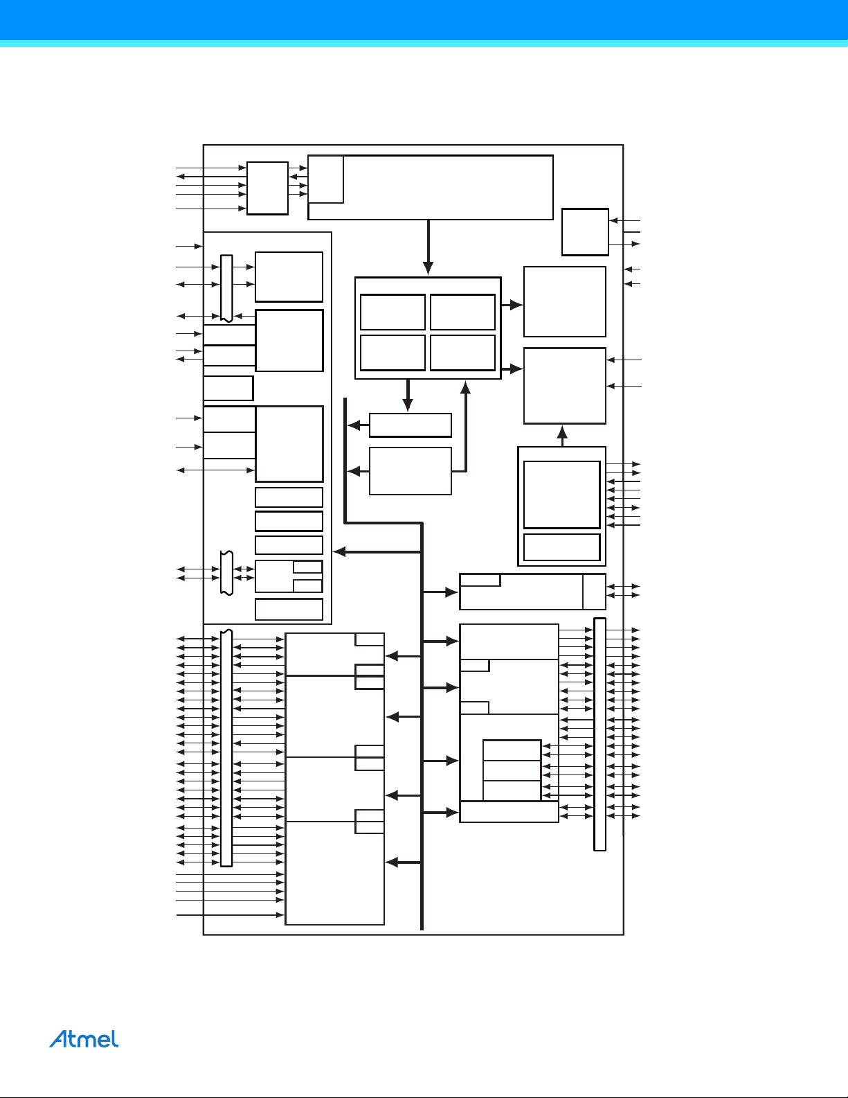
2. Block Diagram
Figure 2-1. SAM7S512/256/128/64/321/161 Block Diagram
SAM7S Series [DATASHEET]
6175M–ATARM–26-Oct-12
4
ROM
TDI
TDO
TMS
TCK
NRST
FIQ
IRQ0
PCK0-PCK2
JTAGSEL
RXD0
TXD0
SCK0
RTS0
CTS0
NPCS0
NPCS1
NPCS2
NPCS3
MISO
MOSI
SPCK
DRXD
DTXD
TF
TK
TD
RD
RK
RF
TCLK0
TIOA0
TIOB0
TIOA1
TIOB1
AD0
AD1
AD2
AD3
ADTRG
PLLRC
9 Channels
ADVREF
TWD
TWCK
XIN
XOUT
VDDIN
PWM0
PWM1
PWM2
PWM3
GND
VDDOUT
VDDCORE
VDDCORE
AD4
AD5
AD6
AD7
VDDFLASH
ERASE
PGMD0-PGMD7
PGMNCMD
PGMEN0-PGMEN2
PGMRDY
PGMNVALID
PGMNOE
PGMCK
PGMM0-PGMM3
VDDIO
TST
VDDCORE
SRAM
8/4 Kbytes
ARM7TDMI
Processor
Flash
32/16 Kbytes
APB
SAM-BA
PMC
Peripheral Bridge
Peripheral DMA
Controller
AIC
PLL
RCOSC
ICE
JTAG
SCAN
PIOA
USART0
SSC
Timer Counter
Reset
Controller
Memory Controller
Abort
Status
Address
Decoder
Misalignment
Detection
PIO
PIO
POR
Embedded
Flash
Controller
PDC
PDC
PDC
PDC
SPI
PDC
ADC
PDC
PDC
TC0
TC1
TC2
TWI
OSC
PWMC
1.8 V
Voltage
Regulator
BOD
Fast Flash
Programming
Interface
PIO
DBGU
PDC
PDC
PIO
PIT
WDT
RTT
System Controller
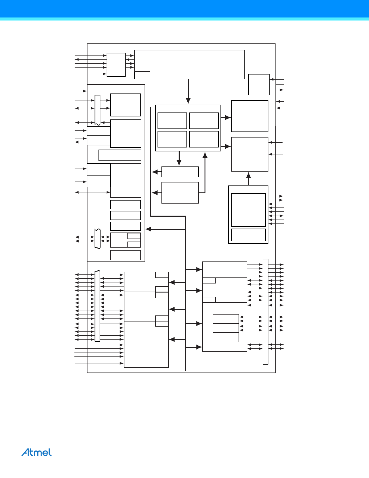
Figure 2-2. SAM7S32/16 Block Diagram
SAM7S Series [DATASHEET]
6175M–ATARM–26-Oct-12
5
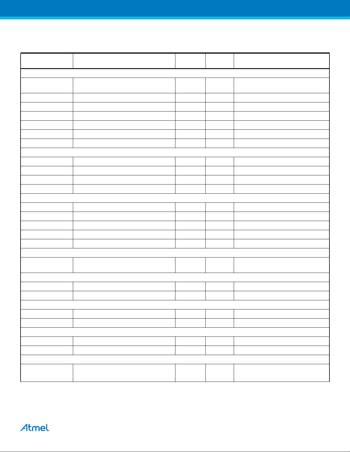
3. Signal Description
Table 3-1. Signal Description List
Active
Signal Name Function Type
Power
VDDIN
Voltage and ADC Regulator Power Supply
Input
Power 3.0 to 3.6V
VDDOUT Voltage Regulator Output Power 1.85V nominal
VDDFLASH Flash Power Supply Power 3.0V to 3.6V
VDDIO I/O Lines Power Supply Power 3.0V to 3.6V or 1.65V to 1.95V
VDDCORE Core Power Supply Power 1.65V to 1.95V
VDDPLL PLL Power 1.65V to 1.95V
GND Ground Ground
Clocks, Oscillators and PLLs
XIN Main Oscillator Input Input
XOUT Main Oscillator Output Output
PLLRC PLL Filter Input
PCK0 - PCK2 Programmable Clock Output Output
ICE and JTAG
TCK Test Clock Input No pull-up resistor
TDI Test Data In Input No pull-up resistor
TDO Test Data Out Output
TMS Test Mode Select Input No pull-up resistor
JTAGSEL JTAG Selection Input Pull-down resistor
Flash Memory
ERASE
Flash and NVM Configuration Bits Erase
Command
Input High Pull-down resistor
Reset/Test
NRST Microcontroller Reset I/O Low Open-drain with pull-Up resistor
TST Test Mode Select Input High Pull-down resistor
Debug Unit
DRXD Debug Receive Data Input
DTXD Debug Transmit Data Output
AIC
IRQ0 - IRQ1 External Interrupt Inputs Input IRQ1 not present on SAM7S32/16
FIQ Fast Interrupt Input Input
PIO
PA0 - PA31 Parallel IO Controller A I/O
Level Comments
(1)
(1)
(1)
Pulled-up input at reset
PA0 - PA20 only on SAM7S32/16
SAM7S Series [DATASHEET]
6175M–ATARM–26-Oct-12
6

Table 3-1. Signal Description List (Continued)
Active
Signal Name Function Type
Level Comments
USB Device Port
DDM USB Device Port Data - Analog not present on SAM7S32/16
DDP USB Device Port Data + Analog not present on SAM7S32/16
USART
SCK0 - SCK1 Serial Clock I/O SCK1 not present on SAM7S32/16
TXD0 - TXD1 Transmit Data I/O TXD1 not present on SAM7S32/16
RXD0 - RXD1 Receive Data Input RXD1 not present on SAM7S32/16
RTS0 - RTS1 Request To Send Output RTS1 not present on SAM7S32/16
CTS0 - CTS1 Clear To Send Input CTS1 not present on SAM7S32/16
DCD1 Data Carrier Detect Input not present on SAM7S32/16
DTR1 Data Terminal Ready Output not present on SAM7S32/16
DSR1 Data Set Ready Input not present on SAM7S32/16
RI1 Ring Indicator Input not present on SAM7S32/16
Synchronous Serial Controller
TD Transmit Data Output
RD Receive Data Input
TK Transmit Clock I/O
RK Receive Clock I/O
TF Transmit Frame Sync I/O
RF Receive Frame Sync I/O
Timer/Counter
TCLK0 - TCLK2 External Clock Inputs Input
TCLK1 and TCLK2 not present on
SAM7S32/16
TIOA0 - TIOA2 I/O Line A I/O TIOA2 not present on SAM7S32/16
TIOB0 - TIOB2 I/O Line B I/O TIOB2 not present on SAM7S32/16
PWM Controller
PWM0 - PWM3 PWM Channels Output
SPI
MISO Master In Slave Out I/O
MOSI Master Out Slave In I/O
SPCK SPI Serial Clock I/O
NPCS0 SPI Peripheral Chip Select 0 I/O Low
NPCS1-NPCS3 SPI Peripheral Chip Select 1 to 3 Output Low
SAM7S Series [DATASHEET]
6175M–ATARM–26-Oct-12
7

Table 3-1. Signal Description List (Continued)
Active
Signal Name Function Type
Level Comments
Two-Wire Interface
TWD Two-wire Serial Data I/O
TWCK Two-wire Serial Clock I/O
Analog-to-Digital Converter
AD0-AD3 Analog Inputs Analog Digital pulled-up inputs at reset
AD4-AD7 Analog Inputs Analog Analog Inputs
ADTRG ADC Trigger Input
ADVREF ADC Reference Analog
Fast Flash Programming Interface
PGMEN0-PGMEN2 Programming Enabling Input
PGMM0-PGMM3 Programming Mode Input
PGMD0-PGMD15 Programming Data I/O PGMD0-PGMD7 only on SAM7S32/16
PGMRDY Programming Ready Output High
PGMNVALID Data Direction Output Low
PGMNOE Programming Read Input Low
PGMCK Programming Clock Input
PGMNCMD Programming Command Input Low
Note: 1. Refer to Section 6. “I/O Lines Considerations” on page 14.
SAM7S Series [DATASHEET]
6175M–ATARM–26-Oct-12
8
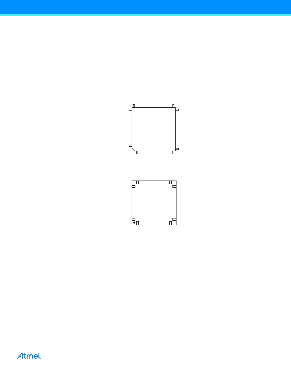
4. Package and Pinout
116
17
32
3348
49
64
3348
161
49
64
32
17
The SAM7S512/256/128/64/321 are available in a 64-lead LQFP or 64-pad QFN package.
The SAM7S161 is available in a 64-Lead LQFP package.
The SAM7S32/16 are available in a 48-lead LQFP or 48-pad QFN package.
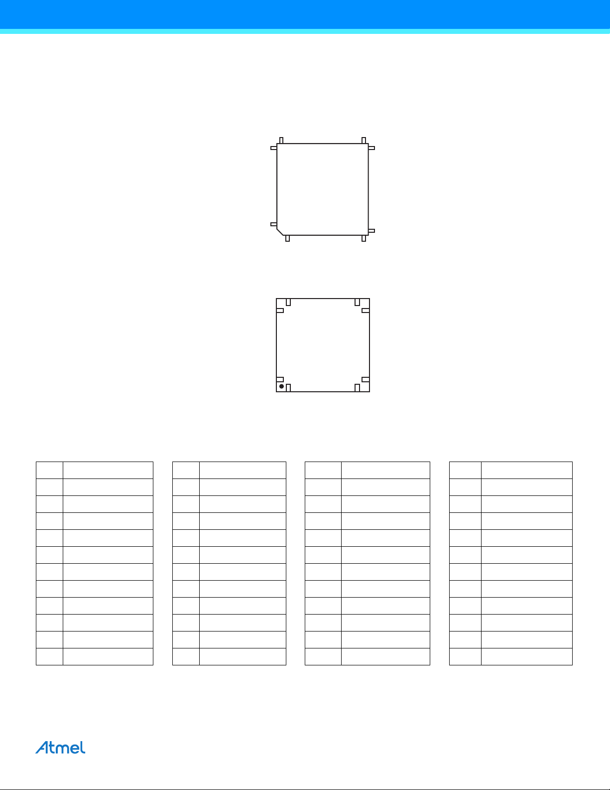
4.1 64-lead LQFP and 64-pad QFN Package Outlines
Figure 4-1 and Figure 4-2 show the orientation of the 64-lead LQFP and the 64-pad QFN package. A detailed
mechanical description is given in the section Mechanical Characteristics of the full datasheet.
Figure 4-1. 64-lead LQFP Package (Top View)
Figure 4-2. 64-pad QFN Package (Top View)
SAM7S Series [DATASHEET]
6175M–ATARM–26-Oct-12
9
4.2 64-lead LQFP and 64-pad QFN Pinout
Table 4-1. SAM7S512/256/128/64/321/161 Pinout
1 ADVREF 17 GND 33 TDI 49 TDO
2 GND 18 VDDIO 34 PA6/PGMNOE 50 JTAGSEL
3 AD4 19 PA16/PGMD4 35 PA5/PGMRDY 51 TMS
4 AD5 20 PA15/PGMD3 36 PA4/PGMNCMD 52 PA31
5 AD6 21 PA14/PGMD2 37 PA27/PGMD15 53 TCK
6 AD7 22 PA13/PGMD1 38 PA28 54 VDDCORE
7 VDDIN 23 PA24/PGMD12 39 NRST 55 ERASE
8 VDDOUT 24 VDDCORE 40 TST 56 DDM
9 PA17/PGMD5/AD0 25 PA25/PGMD13 41 PA29 57 DDP
10 PA18/PGMD6/AD1 26 PA26/PGMD14 42 PA30 58 VDDIO
11 PA21/PGMD9 27 PA12/PGMD0 43 PA3 59 VDDFLASH
12 VDDCORE 28 PA11/PGMM3 44 PA2/PGMEN2 60 GND
13 PA19/PGMD7/AD2 29 PA10/PGMM2 45 VDDIO 61 XOUT
14 PA22/PGMD10 30 PA9/PGMM1 46 GND 62 XIN/PGMCK
15 PA23/PGMD11 31 PA8/PGMM0 47 PA1/PGMEN1 63 PLLRC
16 PA20/PGMD8/AD3 32 PA7/PGMNVALID 48 PA0/PGMEN0 64 VDDPLL
Note: 1. The bottom pad of the QFN package must be connected to ground.
(1)
SAM7S Series [DATASHEET]
6175M–ATARM–26-Oct-12
10
4.3 48-lead LQFP and 48-pad QFN Package Outlines
112
13
24
2536
37
48
2536
121
37
48
24
13
Figure 4-3 and Figure 4-4 show the orientation of the 48-lead LQFP and the 48-pad QFN package. A detailed
mechanical description is given in the section Mechanical Characteristics of the full datasheet.
Figure 4-3. 48-lead LQFP Package (Top View)
Figure 4-4. 48-pad QFN Package (Top View)
4.4 48-lead LQFP and 48-pad QFN Pinout
Table 4-2. SAM7S32/16 Pinout
1 ADVREF 13 VDDIO 25 TDI 37 TDO
2 GND 14 PA16/PGMD4 26 PA6/PGMNOE 38 JTAGSEL
3 AD4 15 PA15/PGMD3 27 PA5/PGMRDY 39 TMS
4 AD5 16 PA14/PGMD2 28 PA4/PGMNCMD 40 TCK
5 AD6 17 PA13/PGMD1 29 NRST 41 VDDCORE
6 AD7 18 VDDCORE 30 TST 42 ERASE
7 VDDIN 19 PA12/PGMD0 31 PA3 43 VDDFLASH
8 VDDOUT 20 PA11/PGMM3 32 PA2/PGMEN2 44 GND
9 PA17/PGMD5/AD0 21 PA10/PGMM2 33 VDDIO 45 XOUT
10 PA18/PGMD6/AD1 22 PA9/PGMM1 34 GND 46 XIN/PGMCK
11 PA19/PGMD7/AD2 23 PA8/PGMM0 35 PA1/PGMEN1 47 PLLRC
12 PA20/AD3 24 PA7/PGMNVALID 36 PA0/PGMEN0 48 VDDPLL
Note: 1. The bottom pad of the QFN package must be connected to ground.
(1)
SAM7S Series [DATASHEET]
6175M–ATARM–26-Oct-12
11

5. Power Considerations
5.1 Power Supplies
The SAM7S Series has six types of power supply pins and integrates a voltage regulator, allowing the device to be
supplied with only one voltage. The six power supply pin types are:
z VDDIN pin. It powers the voltage regulator and the ADC; voltage ranges from 3.0V to 3.6V, 3.3V nominal.
z VDDOUT pin. It is the output of the 1.8V voltage regulator.
z VDDIO pin. It powers the I/O lines and the USB transceivers; dual voltage range is supported. Ranges from 3.0V
to 3.6V , 3 .3V nominal or from 1.65V to 1.95V, 1.8V nominal. Note that supplying less than 3.0V to VDDIO prevents
any use of the USB transceivers.
z VDDFLASH pin. It powers a part of the Flash and is required for the Flash to operate correctly; voltage ranges
from 3.0V to 3.6V, 3.3V nominal.
z VDDCORE pins. They power the logic of the device; voltage ranges from 1.65V to 1.95V, 1.8V typical. It can be
connected to the VDDOUT pin with decoupling capacitor. VDDCORE is required for the device, including its
embedded Flash, to operate correctly.
During startup, core supply voltage (VDDCORE) slope must be superior or equal to 6V/ms.
z VDDPLL pin. It powers the oscillator and the PLL. It can be connected directly to the VDDOUT pin.
No separate ground pins are provided for the different power supplies. Only GND pins are provided and should be
connected as shortly as possible to the system ground plane.
In order to decrease current consumption, if the voltage regulator and the ADC are not used, VDDIN, ADVREF, AD4,
AD5, AD6 and AD7 should be connected to GND. In this case VDDOUT should be left unconnected.
5.2 Power Consumption
The SAM7S Series has a static current of less than 60 µA on VDDCORE at 25°C, including the RC oscillator, the voltage
regulator and the power-on reset. When the brown-out detector is activated, 20 µA static current is added.
The dynamic power consumption on VDDCORE is less than 50 mA at full speed when running out of the Flash. Under
the same conditions, the power consumption on VDDFLASH does not exceed 10 mA.
5.3 Voltage Regulator
The SAM7S Series embeds a voltage regulator that is managed by the System Controller.
In Normal Mode, the voltage regulator consumes less than 100 µA static current and draws 100 mA of output current.
The voltage regulator also has a Low-power Mode. In this mode, it consumes less than 25 µA static current and draws 1
mA of output current.
Adequate output supply decoupling is mandatory for VDDOUT to reduce ripple and avoid oscillations. The best way to
achieve this is to use two capacitors in parallel: one external 470 pF (or 1 nF) NPO capacitor must be connected between
VDDOUT and GND as close to the chip as possible. One external 2.2 µF (or 3.3 µF) X7R capacitor must be connected
between VDDOUT and GND.
Adequate input supply decoupling is mandatory for VDDIN in order to improve startup stability and reduce source voltage
drop. The input decoupling capacitor should be placed close to the chip. For example, two capacitors can be used in
parallel: 100 nF NPO and 4.7 µF X7R.
5.4 Typical Powering Schematics
The SAM7S Series supports a 3.3V single supply mode. The internal regulator is connected to the 3.3V source and its
output feeds VDDCORE and the VDDPLL. Figure 5-1 shows the power schematics to be used for USB bus-powered
systems.
SAM7S Series [DATASHEET]
6175M–ATARM–26-Oct-12
12
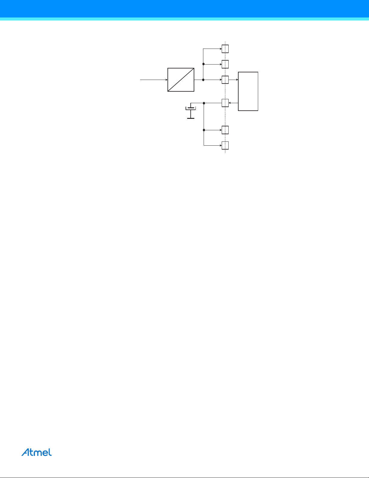
Figure 5-1. 3.3V System Single Power Supply Schematic
Power Source
ranges
from 4.5V (USB)
to 18V
3.3V
VDDIN
Voltage
Regulator
VDDOUT
VDDIO
DC/DC Converter
VDDCORE
VDDFLASH
VDDPLL
SAM7S Series [DATASHEET]
6175M–ATARM–26-Oct-12
13

6. I/O Lines Considerations
6.1 JTAG Port Pins
TMS, TDI and TCK are schmitt trigger inputs. TMS and TCK are 5-V tolerant, TDI is not. TMS, TDI and TCK do not
integrate a pull-up resistor.
TDO is an output, driven at up to VDDIO, and has no pull-up resistor.
The JTAGSEL pin is used to select the JTAG boundary scan when asserted at a high level. The JTAGSEL pin integrates
a permanent pull-down resistor of about 15 kΩ to GND, so that it can be left unconnected for normal operations.
6.2 Test Pin
The TST pin is used for manufacturing test, fast programming mode or SAM-BA Boot Recovery of the SAM7S Series
when asserted high. The TST pin integrates a permanent pull-down resistor of about 15 kΩ to GND, so that it can be left
unconnected for normal operations.
To enter fast programming mode, the TST pin and the PA0 and PA1 pins should be tied high and PA2 tied to low.
To enter SAM-BA Boot Recovery, the TST pin and the PA0, PA1 and PA2 pins should be tied high for at least 10
seconds. Then a power cycle of the board is mandatory.
Driving the TST pin at a high level while PA0 or PA1 is driven at 0 leads to unpredictable results.
6.3 Reset Pin
The NRST pin is bidirectional with an open drain output buffer. It is handled by the on-chip reset controller and can be
driven low to provide a reset signal to the external components or asserted low externally to reset the microcontroller.
There is no constraint on the length of the reset pulse, and the reset controller can guarantee a minimum pulse length.
This allows connection of a simple push-button on the pin NRST as system user reset, and the use of the signal NRST to
reset all the components of the system.
The NRST pin integrates a permanent pull-up resistor to VDDIO.
6.4 ERASE Pin
The ERASE pin is used to re-initialize the Flash content and some of its NVM bits. It integrates a permanent pull-down
resistor of about 15 kΩ to GND, so that it can be left unconnected for normal operations.
6.5 PIO Controller A Lines
z All the I/O lines PA0 to PA31on SAM7S512/256/128/64/321 (PA0 to PA20 on SAM7S32) are 5V-tolerant and all
integrate a programmable pull-up resistor.
z All the I/O lines PA0 to PA31 on SAM7S161 (PA0 to PA20 on SAM7S16) are not 5V-tolerant and all integrate a
programmable pull-up resistor.
Programming of this pull-up resistor is performed independently for each I/O line through the PIO controllers.
5V-tolerant means that the I/O lines can drive voltage level according to VDDIO, but can be driven with a voltage of up to
5.5V. However, driving an I/O line with a voltage over VDDIO while the programmable pull-up resistor is enabled will
create a current path through the pull-up resistor from the I/O line to VDDIO. Care should be taken, in particular at reset,
as all the I/O lines default to input with the pull-up resistor enabled at reset.
6.6 I/O Line Drive Levels
The PIO lines PA0 to PA3 are high-drive current capable. Each of these I/O lines can drive up to 16 mA permanently.
The remaining I/O lines can draw only 8 mA.
However, the total current drawn by all the I/O lines cannot exceed 150 mA (100 mA for SAM7S32/16).
SAM7S Series [DATASHEET]
6175M–ATARM–26-Oct-12
14

SAM7S Series [DATASHEET]
6175M–ATARM–26-Oct-12
15

7. Processor and Architecture
7.1 ARM7TDMI Processor
z RISC processor based on ARMv4T Von Neumann architecture
z Runs at up to 55 MHz, providing 0.9 MIPS/MHz
z Two instruction sets
z ARM
z Thumb
z Three-stage pipeline architecture
z Instruction Fetch (F)
z Instruction Decode (D)
z Execute (E)
7.2 Debug and Test Features
z Integrated EmbeddedICE
z Two watchpoint units
z Test access port accessible through a JTAG protocol
z Debug communication channel
z Debug Unit
z Two-pin UART
z Debug communication channel interrupt handling
z Chip ID Register
z IEEE1149.1 JTAG Boundary-scan on all digital pins
®
high-performance 32-bit instruction set
®
high code density 16-bit instruction set
™
(embedded in-circuit emulator)
7.3 Memory Controller
z Bus Arbiter
z Handles requests from the ARM7TDMI and the Peripheral DMA Controller
z Address decoder provides selection signals for
z Three internal 1 Mbyte memory areas
z One 256 Mbyte embedded peripheral area
z Abort Status Registers
z Source, Type and all parameters of the access leading to an abort are saved
z Facilitates debug by detection of bad pointers
z Misalignment Detector
z Alignment checking of all data accesses
z Abort generation in case of misalignment
z Remap Command
z Remaps the SRAM in place of the embedded non-volatile memory
z Allows handling of dynamic exception vectors
z Embedded Flash Controller
z Embedded Flash interface, up to three programmable wait states
z Prefetch buffer, buffering and anticipating the 16-bit requests, reducing the required wait states
z Key-protected program, erase and lock/unlock sequencer
z Single command for erasing, programming and locking operations
z Interrupt generation in case of forbidden operation
SAM7S Series [DATASHEET]
6175M–ATARM–26-Oct-12
16

7.4 Peripheral DMA Controller
z Handles data transfer between peripherals and memories
z Eleven channels: SAM7S512/256/128/64/321/161
z Nine channels: SAM7S32/16
z Two for each USART
z Two for the Debug Unit
z Two for the Serial Synchronous Controller
z Two for the Serial Peripheral Interface
z One for the Analog-to-digital Converter
z Low bus arbitration overhead
z One Master Clock cycle needed for a transfer from memory to peripheral
z Two Master Clock cycles needed for a transfer from peripheral to memory
z Next Pointer management for reducing interrupt latency requirements
z Peripheral DMA Controller (PDC) priority is as follows (from the highest priority to the lowest):
Receive DBGU
Receive USART0
Receive USART1
Receive SSC
Receive ADC
Receive SPI
Transmit D BGU
Transmit USART0
Transmit USART1
Transmit SSC
Transmit SPI
SAM7S Series [DATASHEET]
6175M–ATARM–26-Oct-12
17

8. Memories
8.1 SAM7S512
z 512 Kbytes of Flash Memory, dual plane
z 2 contiguous banks of 1024 pages of 256 bytes
z Fast access time, 30 MHz single-cycle access in Worst Case conditions
z Page programming time: 6 ms, including page auto-erase
z Page programming without auto-erase: 3 ms
z Full chip erase time: 15 ms
z 10,000 write cycles, 10-year data retention capability
z 32 lock bits, protecting 32 sectors of 64 pages
z Protection Mode to secure contents of the Flash
z 64 Kbytes of Fast SRAM
z Single-cycle access at full speed
8.2 SAM7S256
z 256 Kbytes of Flash Memory, single plane
z 1024 pages of 256 bytes
z Fast access time, 30 MHz single-cycle access in Worst Case conditions
z Page programming time: 6 ms, including page auto-erase
z Page programming without auto-erase: 3 ms
z Full chip erase time: 15 ms
z 10,000 write cycles, 10-year data retention capability
z 16 lock bits, protecting 16 sectors of 64 pages
z Protection Mode to secure contents of the Flash
z 64 Kbytes of Fast SRAM
z Single-cycle access at full speed
8.3 SAM7S128
z 128 Kbytes of Flash Memory, single plane
z 512 pages of 256 bytes
z Fast access time, 30 MHz single-cycle access in Worst Case conditions
z Page programming time: 6 ms, including page auto-erase
z Page programming without auto-erase: 3 ms
z Full chip erase time: 15 ms
z 10,000 write cycles, 10-year data retention capability
z 8 lock bits, protecting 8 sectors of 64 pages
z Protection Mode to secure contents of the Flash
z 32 Kbytes of Fast SRAM
z Single-cycle access at full speed
8.4 SAM7S64
z 64 Kbytes of Flash Memory, single plane
z 512 pages of 128 bytes
SAM7S Series [DATASHEET]
6175M–ATARM–26-Oct-12
18

z Fast access time, 30 MHz single-cycle access in Worst Case conditions
z Page programming time: 6 ms, including page auto-erase
z Page programming without auto-erase: 3 ms
z Full chip erase time: 15 ms
z 10,000 write cycles, 10-year data retention capability
z 16 lock bits, protecting 16 sectors of 32 pages
z Protection Mode to secure contents of the Flash
z 16 Kbytes of Fast SRAM
z Single-cycle access at full speed
8.5 SAM7S321/32
z 32 Kbytes of Flash Memory, single plane
z 256 pages of 128 bytes
z Fast access time, 30 MHz single-cycle access in Worst Case conditions
z Page programming time: 6 ms, including page auto-erase
z Page programming without auto-erase: 3 ms
z Full chip erase time: 15 ms
z 10,000 write cycles, 10-year data retention capability
z 8 lock bits, protecting 8 sectors of 32 pages
z Protection Mode to secure contents of the Flash
z 8 Kbytes of Fast SRAM
z Single-cycle access at full speed
8.6 SAM7S161/16
z 16 Kbytes of Flash Memory, single plane
z 256 pages of 64 bytes
z Fast access time, 30 MHz single-cycle access in Worst Case conditions
z Page programming time: 6 ms, including page auto-erase
z Page programming without auto-erase: 3 ms
z Full chip erase time: 15 ms
z 10,000 write cycles, 10-year data retention capability
z 8 lock bits, protecting 8 sectors of 32 pages
z Protection Mode to secure contents of the Flash
z 4 Kbytes of Fast SRAM
z Single-cycle access at full speed
SAM7S Series [DATASHEET]
6175M–ATARM–26-Oct-12
19
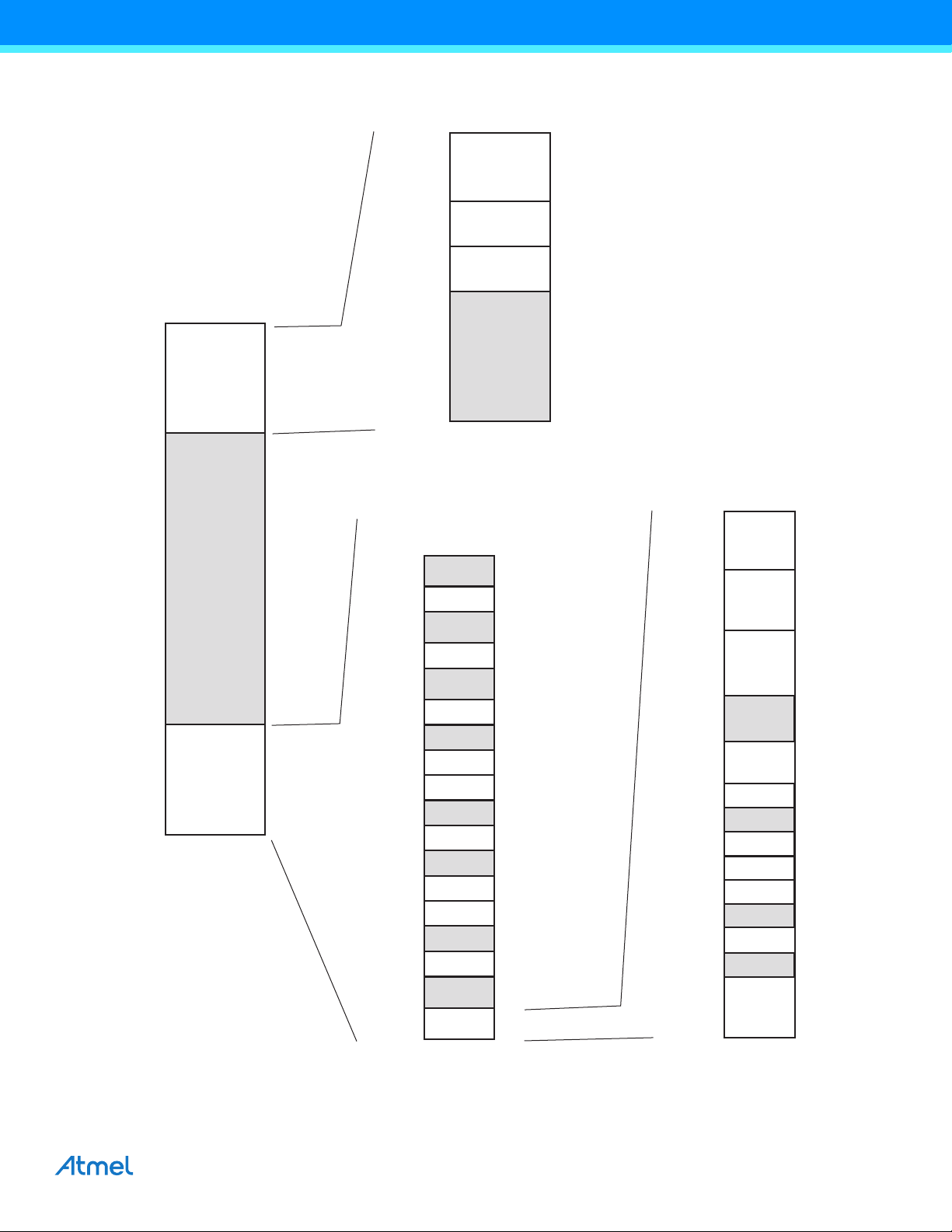
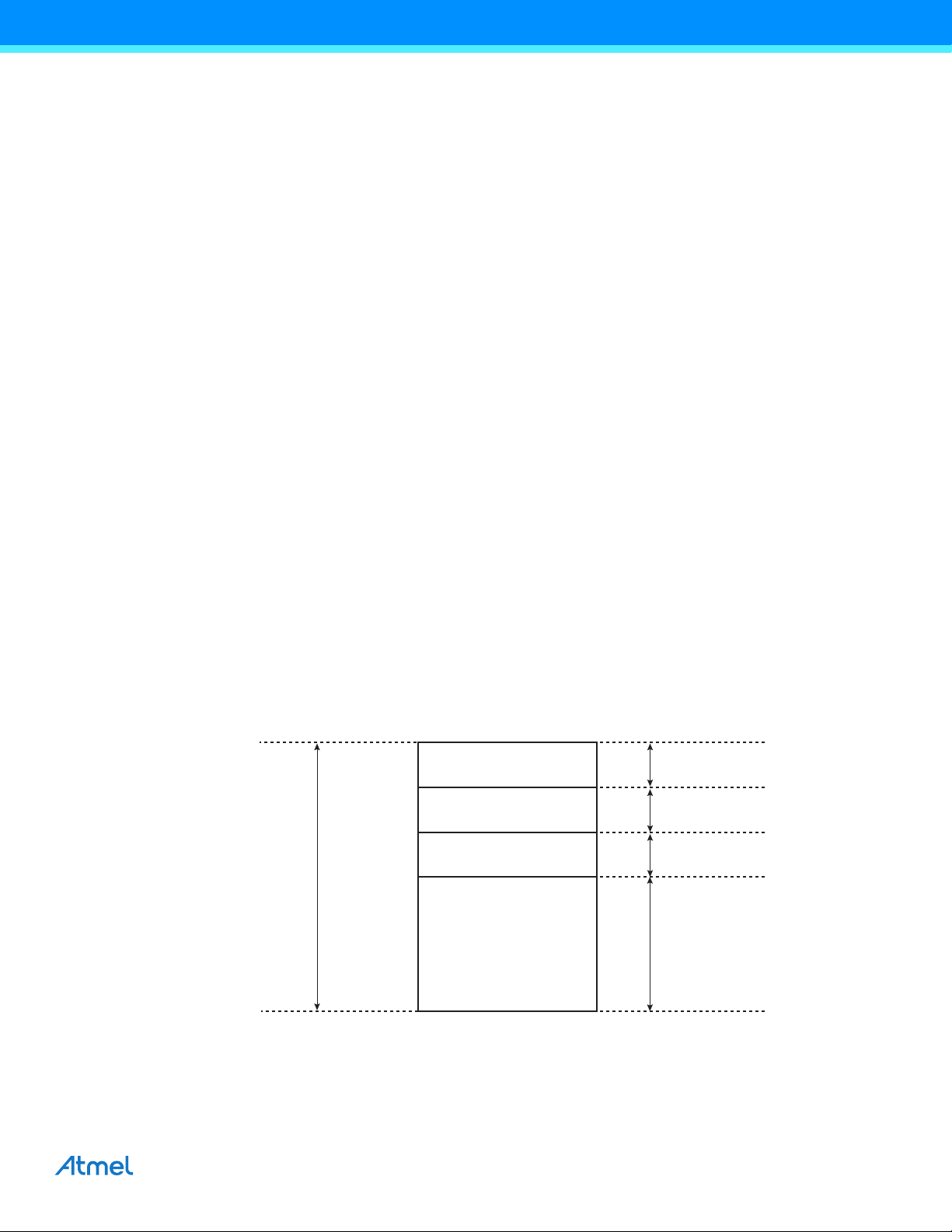
Figure 8-1. SAM7S512/256/128/64/321/32/161/16 Memory Mapping
Internal Memory Mapping
0x0000 0000
Flash before Remap
SRAM after Remap
0x000F FFF
0x0000 0000
Address Memory Space
Internal Memories
256 MBytes
0x0010 0000
0x001F FFF
0x0020 0000
0x002F FFF
0x0030 0000
Internal Flash
Internal SRAM
Reserved
(1)
1 MBytes
1 MBytes
1 MBytes
253 MBytes
Note:
(1) Can be Flash or SRAM
depending on REMAP.
0x0FFF FFFF
0x1000 0000
0xEFFF FFFF
0xF000 0000
0xFFFF FFFF
Undefined
(Abort)
Internal Peripherals
14 x 256 MBytes
3,584 MBytes
256M Bytes
0x0FFF FFFF
0xF000 0000
0xFFF9 FFFF
0xFFFA 0000
0xFFFA 3FFF
0xFFFA 4000
0xFFFA FFFF
0xFFFB 0000
0xFFFB 3FFF
0xFFFB 4000
0xFFFB 7FFF
0xFFFB 8000
0xFFFB BFFF
0xFFFB C000
0xFFFB FFFF
0xFFFC 0000
0xFFFC 3FFF
0xFFFC 4000
0xFFFC 7FFF
0xFFFC 8000
0xFFFC BFFF
0xFFFC C000
0xFFFC FFFF
0xFFFD 0000
0xFFFD 3FFF
0xFFFD 4000
0xFFFD 7FFF
0xFFFD 8000
0xFFFD BFFF
0xFFFD C000
0xFFFD FFFF
0xFFFE 0000
0xFFFE 3FFF
0xFFFE 4000
0xFFFF EFFF
0xFFFF F000
0xFFFF FFFF
Peripheral Mapping
Reserved
TC0, TC1, TC2
Reserved
UDP
Reserved
TWI
Reserved
USART0
USART1
Reserved
PWMC
Reserved
SSC
ADC
Reserved
SPI
Reserved
SYSC
16 Kbytes
16 Kbytes
(Reserved on
SAM7S32/16)
16 Kbytes
16 Kbytes
16 Kbytes
(Reserved on
SAM7S32/16)
16 Kbytes
16 Kbytes
16 Kbytes
16 Kbytes
System Controller Mapping
0xFFFF F000
AIC
0xFFFF F1FF
0xFFFF F200
DBGU
0xFFFF F3FF
0xFFFF F400
PIOA
0xFFFF F5FF
0xFFFF F600
Reserved
0xFFFF FBFF
0xFFFF FC00
0xFFFF FCFF
0xFFFF FD00
0xFFFF FD0F
0xFFFF FD20
0xFFFF FC2F
0xFFFF FD30
0xFFFF FC3F
0xFFFF FD40
0xFFFF FD4F
0xFFFF FD60
0xFFFF FC6F
0xFFFF FD70
0xFFFF FEFF
0xFFFF FF00
0xFFFF FFFF
PMC
RSTC
Reserved
RTT
PIT
WDT
Reserved
VREG
Reserved
MC
512 Bytes/
128 registers
512 Bytes/
128 registers
512 Bytes/
128 registers
256 Bytes/
64 registers
16 Bytes/
4 registers
16 Bytes/
4 registers
16 Bytes/
4 registers
16 Bytes/
4 registers
4 Bytes/
1 register
256 Bytes/
64 registers
SAM7S Series [DATASHEET]
6175M–ATARM–26-Oct-12
20
8.7 Memory Mapping
256 MBytes
Flash Before Remap
SRAM After Remap
Undefined Areas
(Abort)
0x000F FFFF
0x001F FFFF
0x002F FFFF
0x0FFF FFFF
1 MBytes
1 MBytes
1 MBytes
253 MBytes
Internal Flash
Internal SRAM
0x0000 0000
0x0010 0000
0x0020 0000
0x0030 0000
8.7.1 Internal SRAM
z The SAM7S512 embeds a high-speed 64-Kbyte SRAM bank.
z The SAM7S256 embeds a high-speed 64-Kbyte SRAM bank.
z The SAM7S128 embeds a high-speed 32-Kbyte SRAM bank.
z The SAM7S64 embeds a high-speed 16-Kbyte SRAM bank.
z The SAM7S321 embeds a high-speed 8-Kbyte SRAM bank.
z The SAM7S32 embeds a high-speed 8-Kbyte SRAM bank.
z The SAM7S161 embeds a high-speed 4-Kbyte SRAM bank.
z The SAM7S16 embeds a high-speed 4-Kbyte SRAM bank
After reset and until the Remap Command is performed, the SRAM is only accessible at address 0x0020 0000. After
Remap, the SRAM also becomes available at address 0x0.
8.7.2 Internal ROM
The SAM7S Series embeds an Internal ROM. The ROM contains the FFPI and the SAM-BA program.
The internal ROM is not mapped by default.
8.7.3 Internal Flash
z The SAM7S512 features two contiguous banks (dual plane) of 256 Kbytes of Flash.
z The SAM7S256 features one bank (single plane) of 256 Kbytes of Flash.
z The SAM7S128 features one bank (single plane) of 128 Kbytes of Flash.
z The SAM7S64 features one bank (single plane) of 64 Kbytes of Flash.
z The SAM7S321/32 features one bank (single plane) of 32 Kbytes of Flash.
z The SAM7S161/16 features one bank (single plane) of 16 Kbytes of Flash.
At any time, the Flash is mapped to address 0x0010 0000. It is also accessible at address 0x0 after the reset and before
the Remap Command.
Figure 8-2. Internal Memory Ma pping
SAM7S Series [DATASHEET]
6175M–ATARM–26-Oct-12
21

8.8 Embedded Flash
8.8.1 Flash Overview
z The Flash of the SAM7S512 is organized in two banks (dual plane) of 1024 pages of 256 bytes. The 524,288 bytes
are organized in 32-bit words.
z The Flash of the SAM7S256 is organized in 1024 pages (single plane) of 256 bytes. The 262,144 bytes are
organized in 32-bit words.
z The Flash of the SAM7S128 is organized in 512 pages (single plane) of 256 bytes. The 131,072 bytes are
organized in 32-bit words.
z The Flash of the SAM7S64 is organized in 512 pages (single plane) of 128 bytes. The 65,536 bytes are organized
in 32-bit words.
z The Flash of the SAM7S321/32 is organized in 256 pages (single plane) of 128 bytes. The 32,768 bytes are
organized in 32-bit words.
z The Flash of the SAM7S161/16 is organized in 256 pages (single plane) of 64 bytes. The 16,384 bytes are
organized in 32-bit words.
z The Flash of the SAM7S512/256/128 contains a 256-byte write buffer, accessible through a 32-bit interface.
z The Flash of the SAM7S64/321/32/161/16 contains a 128-byte write buffer, accessible through a 32-bit interface.
The Flash benefits from the integration of a power reset cell and from the brownout detector. This prevents code
corruption during power supply changes, even in the worst conditions.
When Flash is not used (read or write access), it is automatically placed into standby mode.
8.8.2 Embedded Flash Controller
The Embedded Flash Controller (EFC) manages accesses performed by the masters of the system. It enables reading
the Flash and writing the write buffer. It also contains a User Interface, mapped within the Memory Controller on the APB.
The User Interface allows:
z programming of the access parameters of the Flash (number of wait states, timings, etc.)
z starting commands such as full erase, page erase, page program, NVM bit set, NVM bit clear, etc.
z getting the end status of the last command
z getting error status
z programming interrupts on the end of the last commands or on errors
The Embedded Flash Controller also provides a dual 32-bit prefetch buffer that optimizes 16-bit access to the Flash. This
is particularly efficient when the processor is running in Thumb mode.
Two EFCs are embedded in the SAM7S512 to control each bank of 256 Kbytes. Dual plane organization allows
concurrent Read and Program. Read from one memory plane may be performed even while program or erase functions
are being executed in the other memory plane.
One EFC is embedded in the SAM7S256/128/64/32/321/161/16 to control the single plane 256/128/64/32/16 Kbytes.
SAM7S Series [DATASHEET]
6175M–ATARM–26-Oct-12
22

8.8.3 Lock Regions
8.8.3.1 SAM7S512
Two Embedded Flash Controllers each manage 16 lock bits to protect 16 regions of the flash against inadvertent flash
erasing or programming commands. The SAM7S512 contains 32 lock regions and each lock region contains 64 pages of
256 bytes. Each lock region has a size of 16 Kbytes.
If a locked-region’s erase or program command occurs, the command is aborted and the LOCKE bit in the MC_FSR
register rises and the interrupt line rises if the LOCKE bit has been written at 1 in the MC_FMR register.
The 16 NVM bits (or 32 NVM bits) are software programmable through the corresponding EFC User Interface. The
command “Set Lock Bit” enables the protection. The command “Clear Lock Bit” unlocks the lock region.
Asserting the ERASE pin clears the lock bits, thus unlocking the entire Flash.
8.8.3.2 SAM7S256
The Embedded Flash Controller manages 16 lock bits to protect 16 regions of the flash against inadvertent flash erasing
or programming commands. The SAM7S256 contains 16 lock regions and each lock region contains 64 pages of 256
bytes. Each lock region has a size of 16 Kbytes.
If a locked-region’s erase or program command occurs, the command is aborted and the LOCKE bit in the MC_FSR
register rises and the interrupt line rises if the LOCKE bit has been written at 1 in the MC_FMR register.
The 16 NVM bits are software programmable through the EFC User Interface. The command “Set Lock Bit” enables the
protection. The command “Clear Lock Bit” unlocks the lock region.
Asserting the ERASE pin clears the lock bits, thus unlocking the entire Flash.
8.8.3.3 SAM7S128
The Embedded Flash Controller manages 8 lock bits to protect 8 regions of the flash against inadvertent flash erasing or
programming commands. The SAM7S128 contains 8 lock regions and each lock region contains 64 pages of 256 bytes.
Each lock region has a size of 16 Kbytes.
If a locked-region’s erase or program command occurs, the command is aborted and the LOCKE bit in the MC_FSR
register rises and the interrupt line rises if the LOCKE bit has been written at 1 in the MC_FMR register.
The 8 NVM bits are software programmable through the EFC User Interface. The command “Set Lock Bit” enables the
protection. The command “Clear Lock Bit” unlocks the lock region.
Asserting the ERASE pin clears the lock bits, thus unlocking the entire Flash.
8.8.3.4 SAM7S64
The Embedded Flash Controller manages 16 lock bits to protect 16 regions of the flash against inadvertent flash erasing
or programming commands. The SAM7S64 contains 16 lock regions and each lock region contains 32 pages of 128
bytes. Each lock region has a size of 4 Kbytes.
If a locked-region’s erase or program command occurs, the command is aborted and the LOCKE bit in the MC_FSR
register rises and the interrupt line rises if the LOCKE bit has been written at 1 in the MC_FMR register.
The 16 NVM bits are software programmable through the EFC User Interface. The command “Set Lock Bit” enables the
protection. The command “Clear Lock Bit” unlocks the lock region.
Asserting the ERASE pin clears the lock bits, thus unlocking the entire Flash.
8.8.3.5 SAM7S321/32
The Embedded Flash Controller manages 8 lock bits to protect 8 regions of the flash against inadvertent flash erasing or
programming commands. The SAM7S321/32 contains 8 lock regions and each lock region contains 32 pages of 128
bytes. Each lock region has a size of 4 Kbytes.
If a locked-region’s erase or program command occurs, the command is aborted and the LOCKE bit in the MC_FSR
register rises and the interrupt line rises if the LOCKE bit has been written at 1 in the MC_FMR register.
SAM7S Series [DATASHEET]
6175M–ATARM–26-Oct-12
23
The 8 NVM bits are software programmable through the EFC User Interface. The command “Set Lock Bit” enables the
protection. The command “Clear Lock Bit” unlocks the lock region.
Asserting the ERASE pin clears the lock bits, thus unlocking the entire Flash.
8.8.3.6 SAM7S161/16
The Embedded Flash Controller manages 8 lock bits to protect 8 regions of the flash against inadvertent flash erasing or
programming commands. The SAM7S161/16 contains 8 lock regions and each lock region contains 32 pages of 64
bytes. Each lock region has a size of 2 Kbytes.
If a locked-region’s erase or program command occurs, the command is aborted and the LOCKE bit in the MC_FSR
register rises and the interrupt line rises if the LOCKE bit has been written at 1 in the MC_FMR register.
The 8 NVM bits are software programmable through the EFC User Interface. The command “Set Lock Bit” enables the
protection. The command “Clear Lock Bit” unlocks the lock region.
Asserting the ERASE pin clears the lock bits, thus unlocking the entire Flash.
Table 8-1 summarizes the configuration of the eight devices.
Table 8-1. Flash Configuration Summary
Device Number of Lock Bits Number of Pages in the Lock Region Page Size
SAM7S512 32 64 256 bytes
SAM7S256 16 64 256 bytes
SAM7S128 8 64 256 bytes
SAM7S64 16 32 128 bytes
SAM7S321/32 8 32 128 bytes
SAM7S161/16 8 32 64 bytes
8.8.4 Security Bit Feature
The SAM7S Series features a security bit, based on a specific NVM Bit. When the security is enabled, any access to the
Flash, either through the ICE interface or through the Fast Flash Programming Interface, is forbidden. This ensures the
confidentiality of the code programmed in the Flash.
This security bit can only be enabled, through the Command “Set Security Bit” of the EFC User Interface. Disabling the
security bit can only be achieved by asserting the ERASE pin at 1, and after a full flash erase is performed. When the
security bit is deactivated, all accesses to the flash are permitted.
It is important to note that the assertion of the ERASE pin should always be longer than 50 ms.
As the ERASE pin integrates a permanent pull-down, it can be left unconnected during normal operation. However, it is
safer to connect it directly to GND for the final application.
8.8.5 Non-volatile Brownout Detector Control
Two general purpose NVM (GPNVM) bits are used for controlling the brownout detector (BOD), so that even after a
power loss, the brownout detector operations remain in their state.
These two GPNVM bits can be cleared or set respectively through the commands “Clear General-purpose NVM Bit” and
“Set General-purpose NVM Bit” of the EFC User Interface.
GPNVM Bit 0 is used as a brownout detector enable bit. Setting the GPNVM Bit 0 enables the BOD, clearing it
disables the BOD. Asserting ERASE clears the GPNVM Bit 0 and thus disables the brownout detector by default.
The GPNVM Bit 1 is used as a brownout reset enable signal for the reset controller. Setting the GPNVM Bit 1
enables the brownout reset when a brownout is detected, Clearing the GPNVM Bit 1 disables the brownout reset.
Asserting ERASE disables the brownout reset by default.
SAM7S Series [DATASHEET]
6175M–ATARM–26-Oct-12
24

8.8.6 Calibration Bits
Eight NVM bits are used to calibrate the brownout detector and the voltage regulator. These bits are factory configured
and cannot be changed by the user. The ERASE pin has no effect on the calibration bits.
8.9 Fast Flash Programming Interface
The Fast Flash Programming Interface allows programming the device through either a serial JTAG interface or through
a multiplexed fully-handshaked parallel port. It allows gang-programming with market-standard industrial programmers.
The FFPI supports read, page program, page erase, full erase, lock, unlock and protect commands.
The Fast Flash Programming Interface is enabled and the Fast Programming Mode is entered when the TST pin and the
PA0 and PA1 pins are all tied high and PA2 is tied low.
8.10 SAM-BA Boot Assistant
The SAM-BA® Boot Recovery restores the SAM-BA Boot in th e fir st t wo s ec tor s o f th e o n -chip Fla sh me m or y. T h e
SAM-BA Boot recovery is performed when the TST pin and t he PA0, PA1 an d PA2 pins ar e all tied high f or 10 seconds. Then, a power cycle of the board is mandatory.
The SAM-BA Boot Assistant is a default Boot Program that provides an easy way to program in situ the on-chip Flash
memory.
The SAM-BA Boot Assistant supports serial communication through the DBGU or through the USB Device Port. (The
SAM7S32/16 have no USB Device Port.)
z Communication through the DBGU supports a wide range of crystals from 3 to 20 MHz via software auto-
detection.
z Communication through the USB Device Port is limited to an 18.432 MHz crystal. (
The SAM-BA Boot provides an interface with SAM-BA Graphic User Interface (GUI).
9. System Controller
The System Controller manages all vital blocks of the microcontroller: interrupts, clocks, power, time, debug and reset.
The System Controller peripherals are all mapped to the highest 4 Kbytes of address space, between addresses 0xFFFF
F000 and 0xFFFF FFFF.
Figure 9-1 on page 26 and Figure 9-2 on page 27 show the product specific System Controller Block Diagrams.
Figure 8-1 on page 20 shows the mapping of the of the User Interface of the System Controller peripherals. Note that the
memory controller configuration user interface is also mapped within this address space.
SAM7S Series [DATASHEET]
6175M–ATARM–26-Oct-12
25
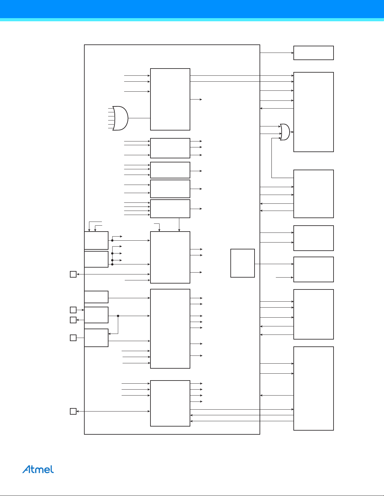
Figure 9-1. System Contro lle r Block Diagram (SAM7S512/256/128/64/321/161)
NRST
SLCK
Advanced
Interrupt
Controller
Real-Time
Timer
Periodic
Interval
Timer
Reset
Controller
PA0-PA31
periph_nreset
System Controller
Watchdog
Timer
wdt_fault
WDRPROC
PIO
Controller
POR
BOD
RCOSC
gpnvm[0]
cal
en
Power
Management
Controller
OSC
PLL
XIN
XOUT
PLLRC
MAINCK
PLLCK
pit_irq
MCK
proc_nreset
wdt_irq
periph_irq{2]periph_nreset
periph_clk[2..14]
PCK
MCK
pmc_irq
UDPCK
nirq
nfiq
rtt_irq
Embedded
Peripherals
periph_clk[2]
pck[0-2]
in
out
enable
ARM7TDMI
SLCK
SLCK
irq0-irq1
fiq
irq0-irq1
fiq
periph_irq[4..14]
periph_irq[2..14]
int
int
periph_nreset
periph_clk[4..14]
Embedded
Flash
flash_poe
jtag_nreset
flash_poe
gpnvm[0..1]
flash_wrdis
flash_wrdis
proc_nreset
periph_nreset
dbgu_txd
dbgu_rxd
pit_irq
rtt_irq
dbgu_irq
pmc_irq
rstc_irq
wdt_irq
rstc_irq
SLCK
gpnvm[1]
Boundary Scan
TAP Controller
jtag_nreset
debug
PCK
debug
idle
debug
Memory
Controller
MCK
proc_nreset
bod_rst_en
proc_nreset
idle
Debug
Unit
dbgu_irq
MCK
dbgu_rxd
periph_nreset
force_ntrst
dbgu_txd
USB Device
Port
UDPCK
periph_nreset
periph_clk[11]
periph_irq[11]
usb_suspend
usb_suspend
Voltage
Regulator
standby
Voltage
Regulator
Mode
Controller
security_bit
cal
power_on_reset
force_ntrst
cal
power_on_reset
power_on_reset
power_on_reset
SAM7S Series [DATASHEET]
6175M–ATARM–26-Oct-12
26
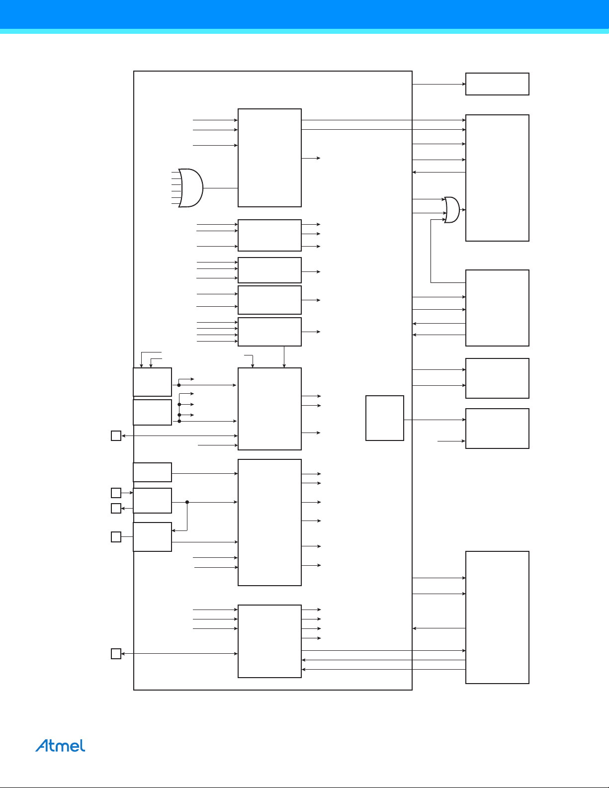
Figure 9-2. System Contro lle r Block Diagram (SAM7S32/16)
NRST
SLCK
Advanced
Interrupt
Controller
Real-Time
Timer
Periodic
Interval
Timer
Reset
Controller
PA0-PA20
periph_nreset
System Controller
Watchdog
Timer
wdt_fault
WDRPROC
PIO
Controller
POR
BOD
RCOSC
gpnvm[0]
cal
en
Power
Management
Controller
OSC
PLL
XIN
XOUT
PLLRC
MAINCK
PLLCK
pit_irq
MCK
proc_nreset
wdt_irq
periph_irq{2]periph_nreset
periph_clk[2..14]
PCK
MCK
pmc_irq
nirq
nfiq
rtt_irq
Embedded
Peripherals
periph_clk[2]
pck[0-2]
in
out
enable
ARM7TDMI
SLCK
SLCK
irq0
fiq
irq0
fiq
periph_irq[4..14]
periph_irq[2..14]
int
int
periph_nreset
periph_clk[4..14]
Embedded
Flash
flash_poe
gpnvm[0..1]
flash_wrdis
proc_nreset
periph_nreset
dbgu_txd
dbgu_rxd
pit_irq
rtt_irq
dbgu_irq
pmc_irq
rstc_irq
wdt_irq
rstc_irq
SLCK
gpnvm[1]
Boundary Scan
TAP Controller
jtag_nreset
debug
PCK
debug
idle
debug
Memory
Controller
MCK
proc_nreset
bod_rst_en
proc_nreset
periph_nreset
idle
Debug
Unit
dbgu_irq
MCK
dbgu_rxd
periph_nreset
force_ntrst
dbgu_txd
Voltage
Regulator
standby
Voltage
Regulator
Mode
Controller
security_bit
cal
force_ntrst
cal
flash_poe
jtag_nreset
power_on_reset
power_on_reset
flash_wrdis
power_on_reset
SAM7S Series [DATASHEET]
6175M–ATARM–26-Oct-12
27

9.1 Reset Controller
The Reset Controller is based on a power-on reset cell and one brownout detector. It gives the status of the last reset,
indicating whether it is a power-up reset, a software reset, a user reset, a watchdog reset or a brownout reset. In addition,
it controls the internal resets and the NRST pin open-drain output. It allows to shape a signal on the NRST line,
guaranteeing that the length of the pulse meets any requirement.
Note that if NRST is used as a reset output signal for external devices during power-off, the brownout detector must be
activated.
9.1.1 Brownout Detector and Power-on Reset
The SAM7S Series embeds a brownout detection circuit and a power-on reset cell. Both are supplied with and monitor
VDDCORE. Both signals are provided to the Flash to prevent any code corruption during power-up or power-down
sequences or if brownouts occur on the VDDCORE power supply.
The power-on reset cell has a limited-accuracy threshold at around 1.5V. Its output remains low during power-up until
VDDCORE goes over this voltage level. This signal goes to the reset controller and allows a full re-initialization of the
device.
The brownout detector monitors the VDDCORE level during operation by comparing it to a fixed trigger level. It secures
system operations in the most difficult environments and prevents code corruption in case of brownout on the
VDDCORE.
Only VDDCORE is monitored.
When the brownout detector is enabled and VDDCORE decreases to a value below the trigger level (Vbot-, defined as
Vbot - hyst/2), the brownout output is immediately activated.
When VDDCORE increases above the trigger level (Vbot+, defined as Vbot + hyst/2), the reset is released. The
brownout detector only detects a drop if the voltage on VDDCORE stays below the threshold voltage for longer than
about 1µs.
The threshold voltage has a hysteresis of about 50 mV, to ensure spike free brownout detection. The typical value of the
brownout detector threshold is 1.68V with an accuracy of ± 2% and is factory calibrated.
The brownout detector is low-power, as it consumes less than 20 µA static current. However, it can be deactivated to
save its static current. In this case, it consumes less than 1µA. The deactivation is configured through the GPNVM bit 0 of
the Flash.
SAM7S Series [DATASHEET]
6175M–ATARM–26-Oct-12
28
9.2 Clock Generator
Embedded
RC
Oscillator
Main
Oscillator
PLL and
Divider
Clock Generator
Power
Management
Controller
XIN
XOUT
PLLRC
Slow Clock
SLCK
Main Clock
MAINCK
PLL Clock
PLLCK
Control
Status
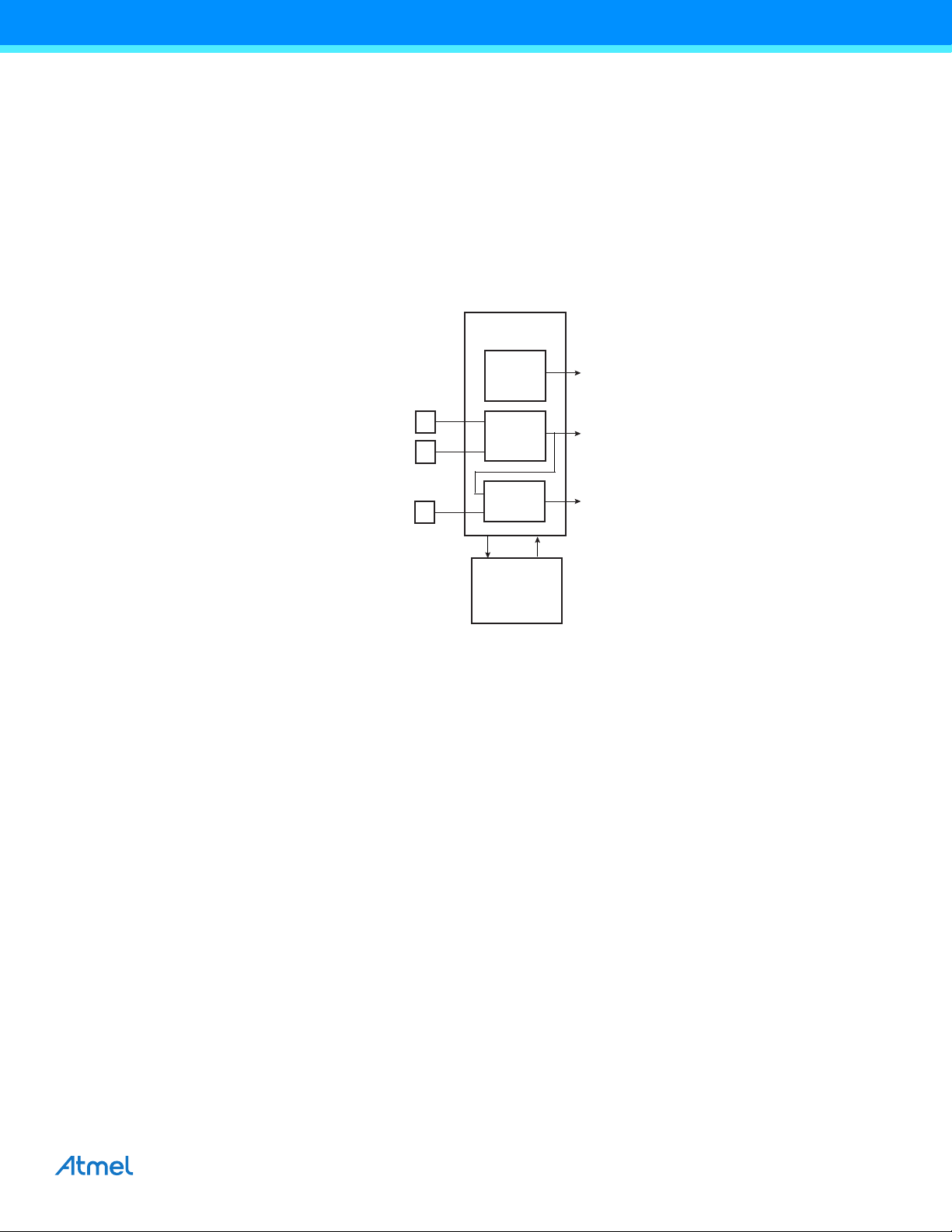
The Clock Generator embeds one low-power RC Oscillator, one Main Oscillator and one PLL with the following
characteristics:
z RC Oscillator ranges between 22 kHz and 42 kHz
z Main Oscillator frequency ranges between 3 and 20 MHz
z Main Oscillator can be bypassed
z PLL output ranges between 80 and 220 MHz
It provides SLCK, MAINCK and PLLCK.
Figure 9-3. Clock Generator Block Diagram
9.3 Power Management Controller
The Power Management Controller uses the Clock Generator outputs to provide:
z the Processor Clock PCK
z the Master Clock MCK
z the USB Clock UDPCK (not present on SAM7S32/16)
z all the peripheral clocks, independently controllable
z three programmable clock outputs
The Master Clock (MCK) is programmable from a few hundred Hz to the maximum operating frequency of the device.
The Processor Clock (PCK) switches off when entering processor idle mode, thus allowing reduced power consumption
while waiting for an interrupt.
SAM7S Series [DATASHEET]
6175M–ATARM–26-Oct-12
29
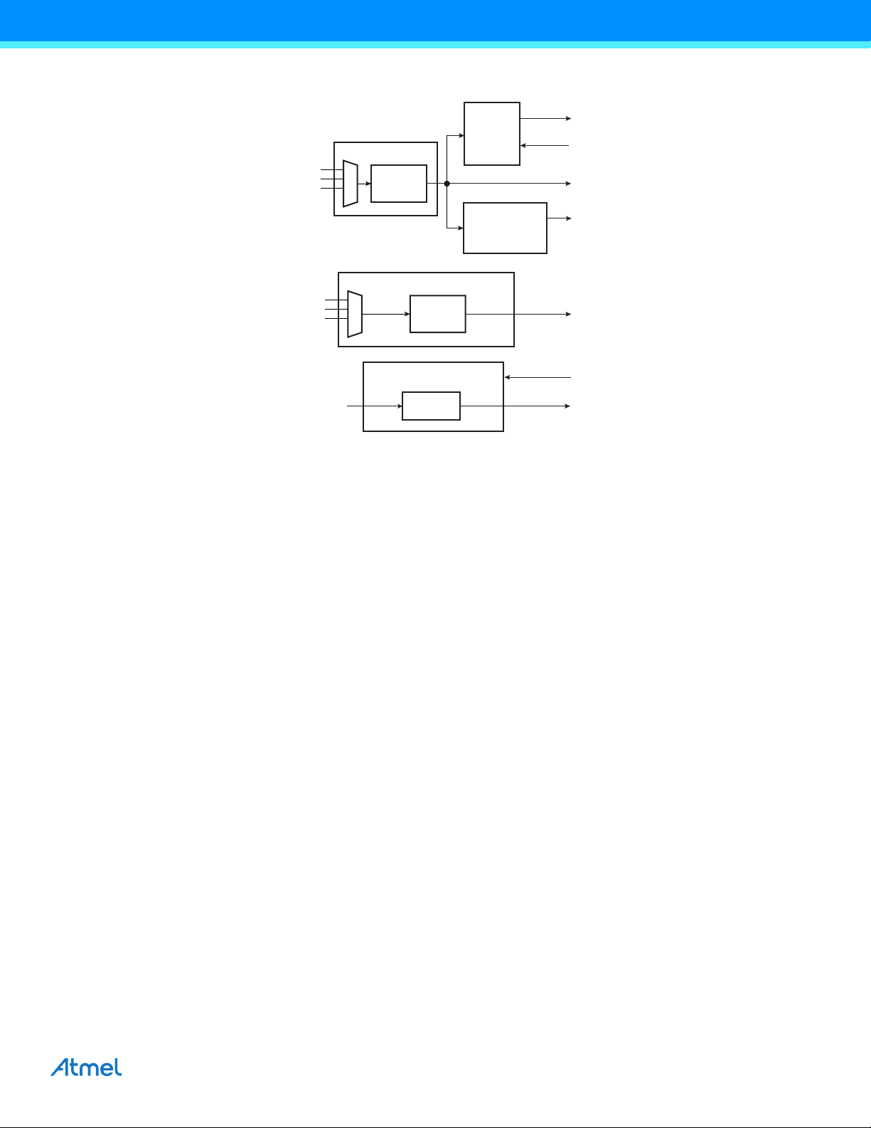
MCK
periph_clk[2..14]
int
UDPCK
usb_suspend
SLCK
MAINCK
PLLCK
Prescaler
/1,/2,/4,...,/64
PCK
Processor
Clock
Controller
Idle Mode
Master Clock Controller
Peripherals
Clock Controller
ON/OFF
USB Clock Controller
ON/OFF
SLCK
MAINCK
PLLCK
Prescaler
/1,/2,/4,...,/64
Programmable Clock Controller
PLLCK
Divider
/1,/2,/4
pck[0..2]
Figure 9-4. Power Management Controller Block Diagra m
9.4 Advanced Interrupt Controller
z Controls the interrupt lines (nIRQ and nFIQ) of an ARM Processor
z Individually maskable and vectored interrupt sources
z Source 0 is reserved for the Fast Interrupt Input (FIQ)
z Source 1 is reserved for system peripherals RTT, PIT, EFC, PMC, DBGU, etc.)
z Other sources control the peripheral interrupts or external interrupts
z Programmable edge-triggered or level-sensitive internal sources
z Programmable positive/negative edge-triggered or high/low level-sensitive external sources
z 8-level Priority Controller
z Drives the normal interrupt of the processor
z Handles priority of the interrupt sources
z Higher priority interrupts can be served during service of lower priority interrupt
z Vectoring
z Optimizes interrupt service routine branch and execution
z One 32-bit vector register per interrupt source
z Interrupt vector register reads the corresponding current interrupt vector
z Protect Mode
z Fast Forcing
z General Interrupt Mask
z Easy debugging by preventing automatic operations
z Permits redirecting any interrupt source on the fast interrupt
z Provides processor synchronization on events without triggering an interrupt
SAM7S Series [DATASHEET]
6175M–ATARM–26-Oct-12
30
 Loading...