

Atmel SAM4SD32B, SAM4SA16C, SAM4S, SAM4SD32C, SAM4SA16B Preliminary Data Sheet
...
Features
• Core
• Pin-to-pin compatible with SAM3N, SAM3S products (64- and 100- pin versions) and
SAM7S legacy products (64-pin version)
• Memories
• System
• Low Power Modes
• Peripherals
• I/O
• Packages
®
– ARM
– Memory Protection Unit (MPU)
– DSP Instruction Set
–Thumb®-2 instruction set
– Up to 2048 Kbytes embedded Flash with optional dual bank and cache memory
– Up to 160 Kbytes embedded SRAM
– 16 Kbytes ROM with embedded boot loader routines (UART, USB) and IAP routines
– 8-bit Static Memory Controller (SMC): SRAM, PSRAM, NOR and NAND Flash
– Embedded volta ge regulato r for single supply operation
– Power -on-Reset (POR), Br own-out Detector (BOD) and Watc hd og for safe operation
– Quartz or ceramic resonator oscillators: 3 to 20 MHz main power with Failure
– RTC with Gregorian and Persian Calendar mode, waveform generation in low-
– RTC clock calibration circuitry for 32.768 kHz crystal frequency compensation
– High precision 8/12 MHz factory trimmed internal RC oscillator with 4 MHz default
– Slow Clock Internal RC oscillator as permanent low-power mode device clock
– Two PLLs up to 240 MHz for device clock and for USB
– Temperature Sensor
– Up to 22 Peripheral DMA (PDC) Channels
– Sleep and Backup modes, down to 1 µA in Backup mode
– Ultra low-power RTC
– USB 2.0 Device: 12 Mbps, 2668 byte FIFO, up to 8 bidirectional Endpoints. On-Chip
– Up to 2 USARTs with ISO7816, IrDA
– Two 2-wire UARTs
– Up to 2 Tw o Wire Interface (I2C compatible), 1 SPI, 1 Serial Synchronous Controller
– 2 Three-Channel 16-bit Timer/Counter with capture, waveform, compare and PWM
– 4-channel 16-bit PWM with Complementary Output, Fault Input, 12-bit Dead Time
– 32-bit Real-time Timer and RTC with calendar and alarm features
– Up to 16-channel, 1Msps ADC with differential input mode and programmable gain
– One 2-channel 12-bit 1Msp s DAC
– One Analog Comparator with flexible input selection, Selectable input hysteresis
– 32-bit Cyclic Redundancy Check Calculation Unit (CRCCU)
– Write Protected Registers
– Up to 79 I/O lines with external interrupt capability (edge or level sensitivity),
– Three 32-bit Parallel Input/Output Controllers, Peripheral DMA assisted Parallel
– 100-lead LQFP, 14 x 14 mm, pitch 0.5 mm/100-ball TFBGA, 9 x 9 mm, pitch
– 64-lead LQFP, 10 x 10 mm, pitch 0.5 mm/64-lead QFN 9x9 mm, pitch 0.5 mm
Cortex®-M4 with a 2 Kbytes cache running at up to 120 MHz
support
Detection and optional low-power 32.768 kHz for RTC or device clock
power modes
frequency for device startup. In-application trimming access for frequency
adjustment
Transceiver
(I2S), 1 High Speed Multimedia Card Interface (SDIO/SD Card/MMC)
mode. Quadrature Decoder Logic and 2-bit Gray Up/Down Counter for Stepper Motor
Generator Counter for Motor Control
stage and auto calibration
debouncing, glitch filtering and on-die Series Resistor Termination
Capture Mode
0.8 mm/100-ball VFBGA, 7 x 7 mm, pitch 0.65 mm
®
, RS-485, SPI, Manchester and Modem Mode
AT91SAM
ARM-based
Flash MCU
SAM4S Series
Preliminary
Datasheet
11100B–ATARM–31-Jul-12

1. Description
The Atmel SAM4S series is a member of a family of Flash microcontrollers based on the high
performance 32-bit ARM Cortex-M4 RISC processor. It operates at a maximum speed of
120 MHz and features up to 2048 Kbytes of Flash, with optional dual bank implementation and
cache memory, and up to 160 Kbytes of SRAM. The peripheral set includes a Full Speed USB
Device port with embedded transceiver, a High Speed MCI for SDIO/SD/MMC, an External Bus
Interface featuring a Static Memory Controller providing connection to SRAM, PSRAM, NOR
Flash, LCD Module and NAND Flash, 2x USARTs, 2x UARTs, 2x TWIs, 3x SPI, an I2S, as well
as 1 PWM timer, 2x three channel general-purpose 16-bit timers (with stepper motor and
quadrature decoder logic support), an RTC, a 12-bit ADC, a 12-bit DAC and an analog
comparator.
The SAM4S series is ready for capacitive touch thanks to the QTouch
way to implement buttons, wheels and sliders.
The SAM4S device is a medium range general purpose microcontroller with the best ratio in
terms of reduced power consumption, processing power and peripheral set. This enables the
SAM4S to sustain a wide range of applications including consumer, industrial control, and PC
peripherals.
It operates from 1.62V to 3.6V.
The SAM4S series is pin-to-pin compatible with the SAM3N, SAM3S series (64- and 100-pin
versions) and SAM7S legacy series (64-pin versions).
®
library, offering an easy
2
SAM4S Series [Preliminary]
11100B–ATARM–31-Jul-12
SAM4S Series [Preliminary]
1.1 Configuration Summary
The SAM4S series devices differ in memory size, package and features. Table 1-1 summarizes
the configurations of the device family.
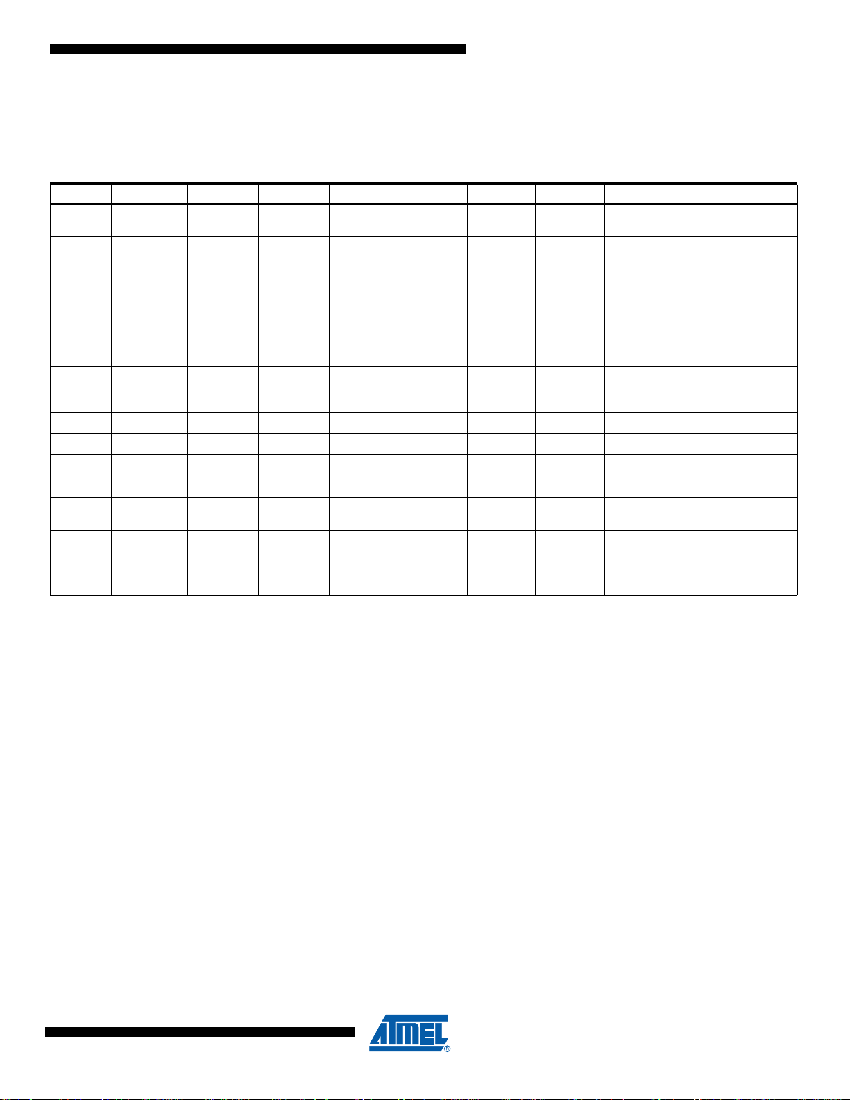
Table 1-1. Configuration Summary
Feature SAM4SD32C SAM4SD32B SAM4SD16C SAM4SD16B SAM4SA16C SAM4SA16B SAM4S16C SAM4S16B SAM4S8C SAM4S8B
Flash
2 x 1024
Kbytes
SRAM 160 Kbytes 160 Kbytes 160 Kbytes 160 Kbytes 160 Kbytes 160 Kbytes 128 Kbytes 128 Kb ytes 128 Kbytes 128 Kbytes
HCACHE 2KBytes 2KBytes 2KBytes 2KBytes 2KBytes 2KBytes - - - -
LQFP 100
TFBGA 100
Package
Number of
PIOs
External
Bus
Interface
12-bit ADC 16 ch.
VFBGA 100
79 47 79 47 79 47 79 47 79 47
8-bit data,
4chip selects,
24-bit address
(1)
12-bit DAC 2 ch. 2 ch. 2 ch. 2 ch. 2 ch. 2 ch. 2 ch. 2 ch. 2 ch. 2 ch.
Timer
Counter
Channels
PDC
Channels
USART/
UART
6363636363
22 22 22 22 22 22 22 22 22 22
(2)
2/2
1 port
HSMCI
4 bits
2 x 1024
Kbytes
LQFP 64
QFN 64
-
(1)
11 ch.
(2)
2/2
1 port
4 bits
2 x 512
Kbytes
LQFP 100
TFBGA 100
VFBGA 100
8-bit data,
4chip selects,
24-bit address
(1)
16 ch.
(2)
2/2
1 port
4 bits
2 x 512
Kbytes
LQFP 64
QFN 64
-
11 ch.
(2)
2/2
1 port
4 bits
1024 Kbytes 1024 Kbytes 1024 Kbytes
LQFP 100
TFBGA 100
VFBGA 100
LQFP 64
QFN 64
8-bit data,
(1)
4chip selects,
24-bit address
(1)
16 ch.
(2)
2/2
1 port
4 bits
11 ch.
2/2
1 port
4 bits
-
(1)
(2)
LQFP 100
TFBGA 100
VFBGA 100
8-bit data,
4chip selects,
24-bit address
(1)
16 ch.
(2)
2/2
1 port
4 bits
1024
Kbytes
LQFP 64
QFN 64
-
(1)
11 ch.
(2)
2/2
1 port
4 bits
512 Kbytes 512 Kbytes
LQFP 100
TFBGA 100
VFBGA 100
LQFP 64
QFN 64
8-bit data,
4chip selects,
24-bit address
(1)
16 ch.
2/2
(2)
11 ch.
1 port
4 bits
-
2/2
1 port
4 bits
(1)
(2)
Notes: 1. One channel is reserved for internal temperature sensor.
2. Full Modem support on USART1.
11100B–ATARM–31-Jul-12
3
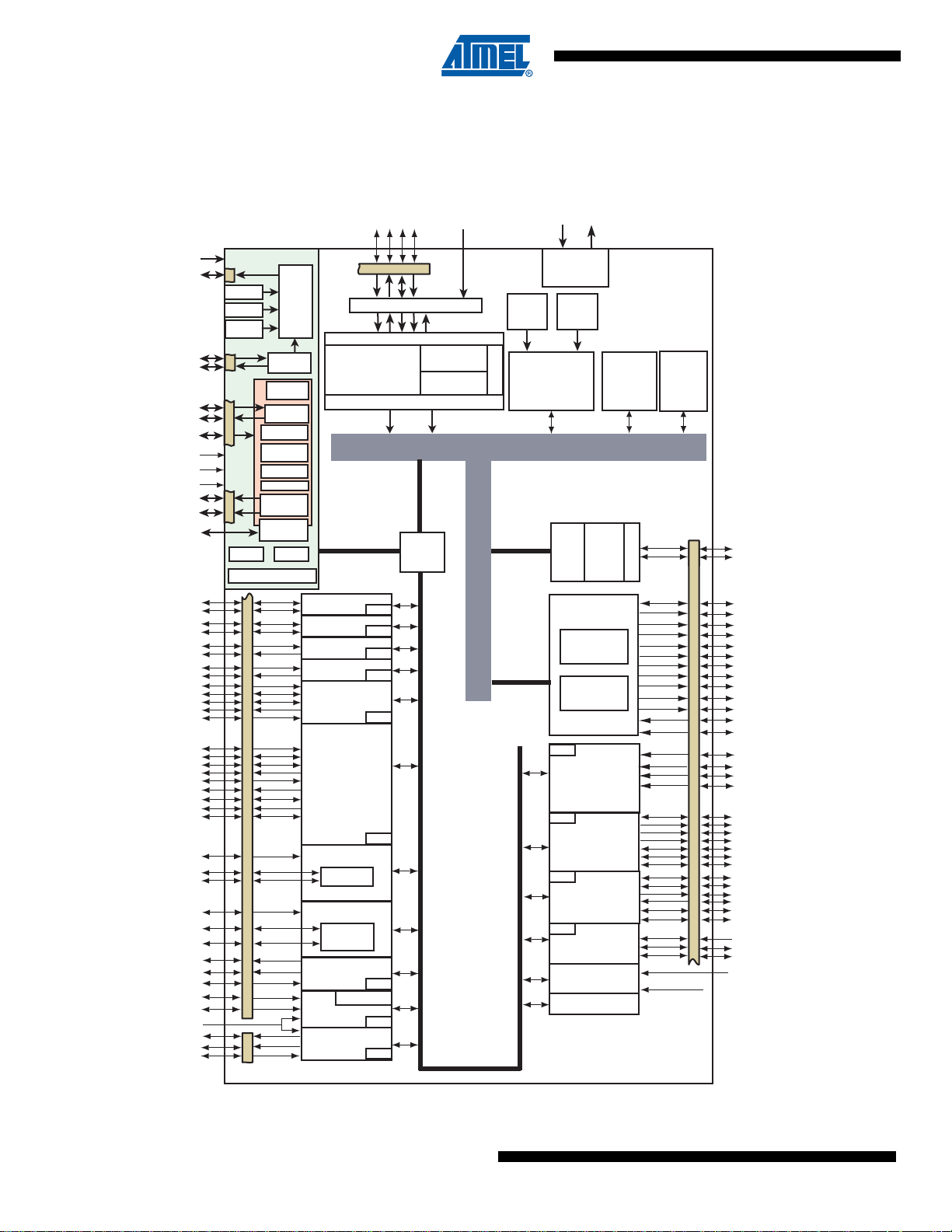
2. Block Diagram
PLLA
System C ontroller
WDT
RTT
Osc 32 kHz
SUPC
RSTC
8 GPBREG
3-20 MHz
Osc
POR
RTC
RC 32 kHz
SM
RC Osc
12/8/4 MHz
I/D
S
MPU
N
V
I
C
4-layer AHB Bus Matrix Fmax 120 MHz
ADC Ch.
PLLB
PMC
PIOA / PIOB / PIOC
PIO
External Bus
Interface
D[7:0]
PIODC[7:0]
A[0:23]
A21/NANDALE
A22/NANDCLE
NCS0
NCS1
NCS2
NCS3
NRD
NWE
NANDOE
NANDWE
NWAIT
High Speed MCI
DATRG
PDC
PDC
PDC
PDC
PDC
PDC
PDC
PDC
PDC
PDC
PDC
PDC
PDC
DAC0
DAC1
Timer Counter B
Timer Counter A
TC[3..5]
TC[0..2]
TIOA[3:5]
TIOB[3:5]
TCLK[3:5]
AD[0..14]
RXD1
TXD1
USART1
USART0
UART1
UART0
SCK1
RTS1
CTS1
DSR1
DTR1
RI1
DCD1
NAND Flash
Logic
TWCK0
TWD0
TWD1
URXD0
UTXD0
URXD1
UTXD1
RXD0
TXD0
SCK0
RTS0
CTS0
TWCK1
ADVREF
TIOB[0:2]
TCLK[0:2]
PWMH[0:3]
PWML[0:3]
PWMFI0
ADTRG
TIOA[0:2]
TST
PCK0-PCK2
XIN
NRST
VDDCORE
XOUT
RTCOUT0
RTCOUT1
XIN32
XOUT32
ERASE
VDDPLL
VDDIO
12-bit DAC
Temp. Sensor
PWM
12-bit ADC
TWI0
TWI1
SPI
SSC
PIO
Static Memory
Controller
Analog
Comparator
CRC Unit
Peripheral
Bridge
2668
Bytes
FIFO
USB 2.0
Full
Speed
Transceiver
NPCS0
PIODCCLK
PIODCEN1
PIODCEN2
NPCS1
NPCS2
NPCS3
MISO
MOSI
SPCK
MCDA[0..3]
MCCDA
MCCK
TF
TK
TD
RD
RK
RF
DDP
DDM
ADVREF
ROM
16 Kbytes
FLASH
1024 Kbytes
512 Kbytes
Flash
Unique
Identifier
User
Signature
TDI
TDO
TMS/SWDIO
TCK/SWCLK
JTAGSEL
Voltage
Regulator
VDDIN
VDDOUT
Cortex-M4 Processor
Fmax 120 MHz
In-Circuit Emulator
JTAG & Serial Wire
24-Bit
SysTick Counter
DSP
SRAM
128 Kbytes
Figure 2-1. SAM4S16, S8 Series 100-pin version Block Diagram
4
SAM4S Series [Preliminary]
11100B–ATARM–31-Jul-12
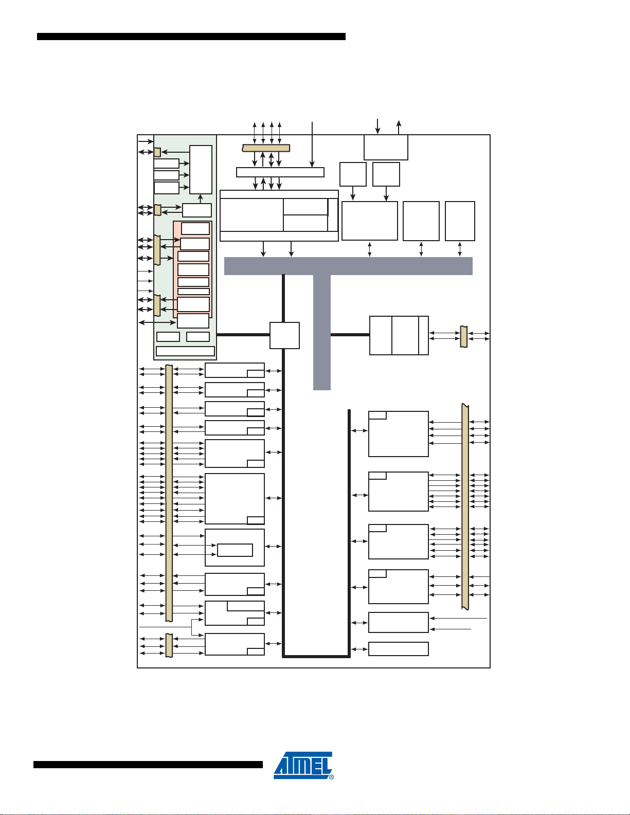
Figure 2-2. SAM4S16, S8 Series 64-pin version Block Diagram
PLLA
System C ontroller
WDT
RTT
Osc 32 kHz
SUPC
RSTC
8 GPBREG
3-20 MHz
Osc
POR
RTC
RC 32 kHz
SM
RC Osc
12/8/4 MHz
I/D
S
MPU
N
V
I
C
4-layer AHB Bus Matrix Fmax 120 MHz
ADC Ch.
PLLB
PMC
PIOA / PIOB
PIODC[7:0]
High Speed MCI
DATRG
PDC
PDC
PDC
PDC
PDC
PDC
PDC
PDC
PDC
PDC
PDC
PDC
PDC
DAC0
DAC1
Timer Counter A
TC[0..2]
AD[0..9]
RXD1
TXD1
USART1
USART0
UART1
UART0
SCK1
RTS1
CTS1
DSR1
DTR1
RI1
DCD1
TWCK0
TWD0
TWD1
URXD0
UTXD0
URXD1
UTXD1
RXD0
TXD0
SCK0
RTS0
CTS0
TWCK1
ADVREF
TIOB[0:2]
TCLK[0:2]
PWMH[0:3]
PWML[0:3]
PWMFI0
ADTRG
TIOA[0:2]
TST
PCK0-PCK2
XIN
NRST
VDDCORE
XOUT
RTCOUT0
RTCOUT1
XIN32
XOUT32
ERASE
VDDPLL
VDDIO
12-bit DAC
Temp. Sensor
PWM
12-bit ADC
TWI0
TWI1
SPI
SSC
PIO
Analog
Comparator
CRC Unit
Peripheral
Bridge
2668
Bytes
FIFO
USB 2.0
Full
Speed
Transceiver
NPCS0
PIODCCLK
PIODCEN1
PIODCEN2
NPCS1
NPCS2
NPCS3
MISO
MOSI
SPCK
MCDA[0..3]
MCCDA
MCCK
TF
TK
TD
RD
RK
RF
DDP
DDM
ADVREF
TDI
TDO
TMS/SWDIO
TCK/SWCLK
JTAGSEL
Voltage
Regulator
VDDIN
VDDOUT
Cortex-M4 Processor
Fmax 120 MHz
In-Circuit Emulator
JTAG & Serial Wire
24-Bit
SysTick Counter
PIO
PIO
DSP
ROM
16 Kbytes
FLASH
1024 Kbytes
512 Kbytes
Flash
Unique
Identifier
User
Signature
SRAM
128 Kbytes
SAM4S Series [Preliminary]
11100B–ATARM–31-Jul-12
5
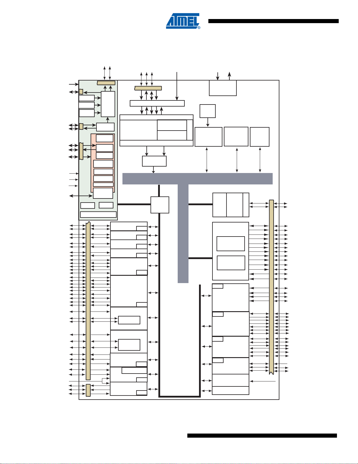
Figure 2-3. SAM4SD32, SD16, SA16 100-pin version Block Diagram
PLLA
TST
PCK0-PCK2
XIN
NRST
VDDCORE
XOUT
WDT
RTT
OSC 32k
XIN32
XOUT32
SUPC
RSTC
8 GPBREG
3-20 MHz
Osc.
POR
RTC
RC 32k
SM
RC
12/8/4 M
ERASE
TDI
TDO
TMS/SWDIO
TCK/SWCLK
JTAGSEL
I
D
Volt age
Regulator
VDDIN
VDDOUT
SPI
TC[0..2]
DAC
ADVREF
PDC
NPCS0
PIODCCLK
PIODCEN1
PIODCEN2
NPCS1
NPCS2
NPCS3
MISO
MOSI
SPCK
MCDA[0..3]
MCCDA
MCCK
TCLK[0:2]
Temp. Sensor
PDC
TWI0
PDC
TWD0
PWM
PDC
TF
TK
TD
RD
RK
RF
DDP
DDM
MPU
N
V
I
C
24-Bit
SysTick Counter
4-layer AHB Bus Matrix Fmax 120 MHz
TWI1
PDC
TWCK1
TWD1
PWMH[0:3]
PWML[0:3]
PWMFI0
PDC
UART0
UART1
URXD0
UTXD0
URXD1
UTXD1
SSC
Peripheral
Bridge
PDC
PIO
PDC
PDC
2668
Bytes
FIFO
USB 2.0
Full
Speed
VDDPLL
VDDIO
PDC
RXD0
TXD0
USART0
SCK0
RTS0
CTS0
Analog
Comparator
CRC Unit
ADC
Transceiver
PLLB
In-Circuit Emulator
JTAG & Serial Wire
Flash
Unique
Identifier
PMC
PIOA / PIOB / PIOC
ADTRG
Cortex-M4 Processor
Fmax 120 MHz
Timer Counter A
Timer Counter B
TWCK0
FLASH
2*1024 KBytes
2*512 KBytes
1024 KBytes
SRAM
160 KBytes
ROM
16 KBytes
RTCOUT1
RTCOUT0
DSP
CMCC
(2 KB cache)
PIO
External Bus
Interface
D[7:0]
PIODC[7:0]
A[0:23]
A21/NANDALE
A22/NANDCLE
NCS0
NCS1
NCS2
NCS3
NRD
NWE
NANDOE
NANDWE
NWAIT
High Speed MCI
PDC
DATRG
PDC
DAC0
DAC1
TC[3..5]
TIOA[3:5]
TIOB[3:5]
TIOA[0:2]
TIOB[0:2]
TCLK[3:5]
AD[0..14]
PDC
RXD1
TXD1
USART1
SCK1
RTS1
CTS1
DSR1
DTR1
RI1
DCD1
NAND Flash
Logic
Static Memory
Controller
ADC
DAC
Temp Sensor
ADVREF
6
SAM4S Series [Preliminary]
11100B–ATARM–31-Jul-12
Figure 2-4. SAM4SD32, SD16, SA16 64-pin version Block Diagram
PLLA
System C ontroller
WDT
RTT
Osc 32 kHz
SUPC
RSTC
8 GPBREG
3-20 MHz
Osc
POR
RTC
RC 32 kHz
SM
RC Osc
12/8/4 MHz
MPU
N
V
I
C
4-layer AHB Bus Matrix Fmax 120 MHz
ADC Ch.
PLLB
PMC
PIOA / PIOB
PIODC[7:0
High Speed MCI
DATRG
PDC
PDC
PDC
PDC
PDC
PDC
PDC
PDC
PDC
PDC
PDC
PDC
PDC
DAC0
DAC1
Timer Counter A
TC[0..2]
AD[0..9]
RXD1
TXD1
USART1
USART0
UART1
UART0
SCK1
RTS1
CTS1
DSR1
DTR1
RI1
DCD1
TWCK0
TWD0
TWD1
URXD0
UTXD0
URXD1
UTXD1
RXD0
TXD0
SCK0
RTS0
CTS0
TWCK1
ADVREF
TIOB[0:2]
TCLK[0:2]
PWMH[0:3]
PWML[0:3]
PWMFI0
ADTRG
TIOA[0:2]
TST
PCK0-PCK2
XIN
NRST
VDDCORE
XOUT
RTCOUT0
RTCOUT1
XIN32
XOUT32
ERASE
VDDPLL
VDDIO
12-bit DAC
Temp. Sensor
PWM
12-bit ADC
TWI0
TWI1
SPI
SSC
PIO
Analog
Comparator
CRC Unit
Peripheral
Bridge
2668
Bytes
FIFO
USB 2.0
Full
Speed
Transceiver
NPCS0
PIODCCLK
PIODCEN
PIODCEN2
NPCS1
NPCS2
NPCS3
MISO
MOSI
SPCK
MCDA[0..3
MCCDA
MCCK
TF
TK
TD
RD
RK
RF
DDP
DDM
ADVREF
Flash
Unique
Identifier
TDI
TDO
TMS/SWDIO
TCK/SWCLK
JTAGSEL
Voltage
Regulator
VDDIN
VDDOUT
Cortex-M4 Processor
Fmax 120 MHz
In-Circuit Emulator
JTAG & Serial Wire
24-Bit
SysTick Counter
PIO
PIO
DSP
ROM
16 KBytes
I
D
FLASH
2*1024 KBytes
2*512 KBytes
1024 KBytes
SRAM
160 KBytes
CMCC
(2 KB cache)
SAM4S Series [Preliminary]
11100B–ATARM–31-Jul-12
7
3. Signal Description
Table 3-1 gives details on signal names classified by peripheral.
Table 3-1. Signal Description List
Signal Name Function Type
Active
Level
Voltage
reference Comments
Power Supplies
VDDIO
VDDIN
Peripherals I/O Lines and USB transceiver
Power Supply
Voltage Regulator Input, ADC, DAC and
Analog Comparator Power Supply
Power 1.62V to 3.6V
Power 1.62V to 3.6V
VDDOUT Voltage Regulator Output Power 1.2V Output
VDDPLL Oscillator and PLL Power Supply Power 1.08 V to 1.32V
VDDCORE
Power the core, the embedded memories
and the peripherals
Power
1.08V to 1.32V
GND Ground Ground
Clocks, Oscillators and PLLs
XIN Main Oscillator Input Input
XOUT Main Oscillator Output Output
XIN32 Slow Clock Oscillator Input Input
XOUT32 Slow Clock Oscillator Output Output
VDDIO
Reset State:
- PIO Input
- Internal Pull-up disabled
- Schmitt Trigger enabled
Reset State:
PCK0 - PCK2 Programmable Clock Output Output
- PIO Input
- Internal Pull-up enabled
- Schmitt Trigger enabled
(4)
(1)
(1)
Real Time Clock
RTCOUT0 Programmable RTC waveform output Output
RTCOUT1 Programmable RTC waveform output Output
Serial Wire/JTAG Debug Port - SWJ-DP
TCK/SWCLK Test Clock/Serial Wire Clock Input
TDI Test Dat a In Input
TDO/TRACESWO
Test Data Out / Trace Asynchronous Data
Out
Output
TMS/SWDIO Test Mode Select /Serial Wire Input/Output Input / I/O
JTA G SEL JTA G Selection Input High
8
SAM4S Series [Preliminary]
VDDIO
VDDIO
Reset State:
- PIO Input
- Internal Pull-up enabled
- Schmitt Trigger enabled
Reset State:
- SWJ-DP Mode
- Internal pull-up disabled
- Schmitt Trigger enabled
Permanent Internal
pull-down
11100B–ATARM–31-Jul-12
(1)
(5)
(1)
Table 3-1. Signal Description List (Continued)
SAM4S Series [Preliminary]
Active
Signal Name Function Type
Level
Flash Memory
ERASE
Flash and NVM Configuration Bits Erase
Command
Input High VDDIO
Reset/Test
NRST Synchronous Microcontroller Reset I/O Low
TST Test Select Input
Universal Asynchronous Receiver Transceiver - UARTx
URXDx UART Receive Data Input
UTXDx UART Transmit Data Output
PIO Controller - PIOA - PIOB - PIOC
PA0 - PA31 Parallel IO Controller A I/O
PB0 - PB14 Parallel IO Controller B I/O
PC0 - PC31 Parallel IO Controller C I/O
Voltage
reference Comments
Reset State:
- Erase Input
- Internal pull-down enabled
- Schmitt Trigger enabled
Permanent Internal
VDDIO
pull-up
Permanent Internal
pull-down
Reset State:
VDDIO
- PIO or System IOs
- Internal pull-up enabled
- Schmitt Trigger enabled
(1)
(2)
(1)
PIO Controller - Parallel Capture Mode
PIODC0-PIODC7 Parallel Capture Mode Data Input
PIODCEN1-2 Parallel Capture Mode Enable Input
External Bus Interface
D0 - D7 Data Bus I/O
A0 - A23 Address Bus Output
NWAIT External Wait Signal Input Low
Static Memory Controller - SMC
NCS0 - NCS3 Chip Select Lines Output Low
NRD Read Signal Output Low
NWE Write Enable Output Low
NAND Flash Logic
NANDOE NAND Flash Output Enable Output Low
NANDWE NAND Flash Write Enable Output Low
High Speed Multimedia Card Interface - HSMCI
MCCK Multimedia Card Clock I/O
MCCDA Multimedia Card Slot A Command I/O
MCDA0 - MCDA3 Multimedia Card Slot A Data I/O
VDDIOPIODCCLK Parallel Capture Mode Clock Input
11100B–ATARM–31-Jul-12
9
Table 3-1. Signal Description List (Continued)
Signal Name Function Type
Universal Synchronous Asynchronous Receiver Transmitter USARTx
SCKx USARTx Serial Clock I/O
TXDx USARTx Transmit Data I/O
RXDx USARTx Receive Data Input
RTSx USARTx Request To Send Output
CTSx USARTx Clear To Send Input
DTR1 USART1 Data Terminal Ready I/O
DSR1 USART1 Data Set Ready Input
DCD1 USART1 Data Carrier Detect Output
RI1 USART1 Ring Indicator Input
Synchronous Serial Controller - SSC
TD SSC Transmit Data Output
RD SSC Receive Data Input
TK SSC Transmit Clock I/O
RK SSC Receive Clock I/O
TF SSC Transmit Frame Sync I/O
RF SSC Receive Frame Sync I/O
Timer/Counter - TC
Active
Level
Voltage
reference Comments
TCLKx TC Channel x External Clock Input Input
TIOAx TC Channel x I/O Line A I/O
TIOBx TC Channel x I/O Line B I/O
Pulse Width Modulation Controller- PWMC
PWMHx PWM Waveform Output High for channel x Output
PWMLx PWM Waveform Output Low for channel x Output
PWMFI0 PWM Fault Input Input
Serial Peripheral Interface - SPI
MISO Master In Slave Out I/O
MOSI Master Out Slave In I/O
SPCK SPI Serial Clock I/O
SPI_NPCS0 SPI Peripheral Chip Select 0 I/O Low
SPI_NPCS1 -
SPI_NPCS3
SPI Peripheral Chip Select Output Low
only output in
complementary mode
when dead time insertion
is enabled.
10
SAM4S Series [Preliminary]
11100B–ATARM–31-Jul-12
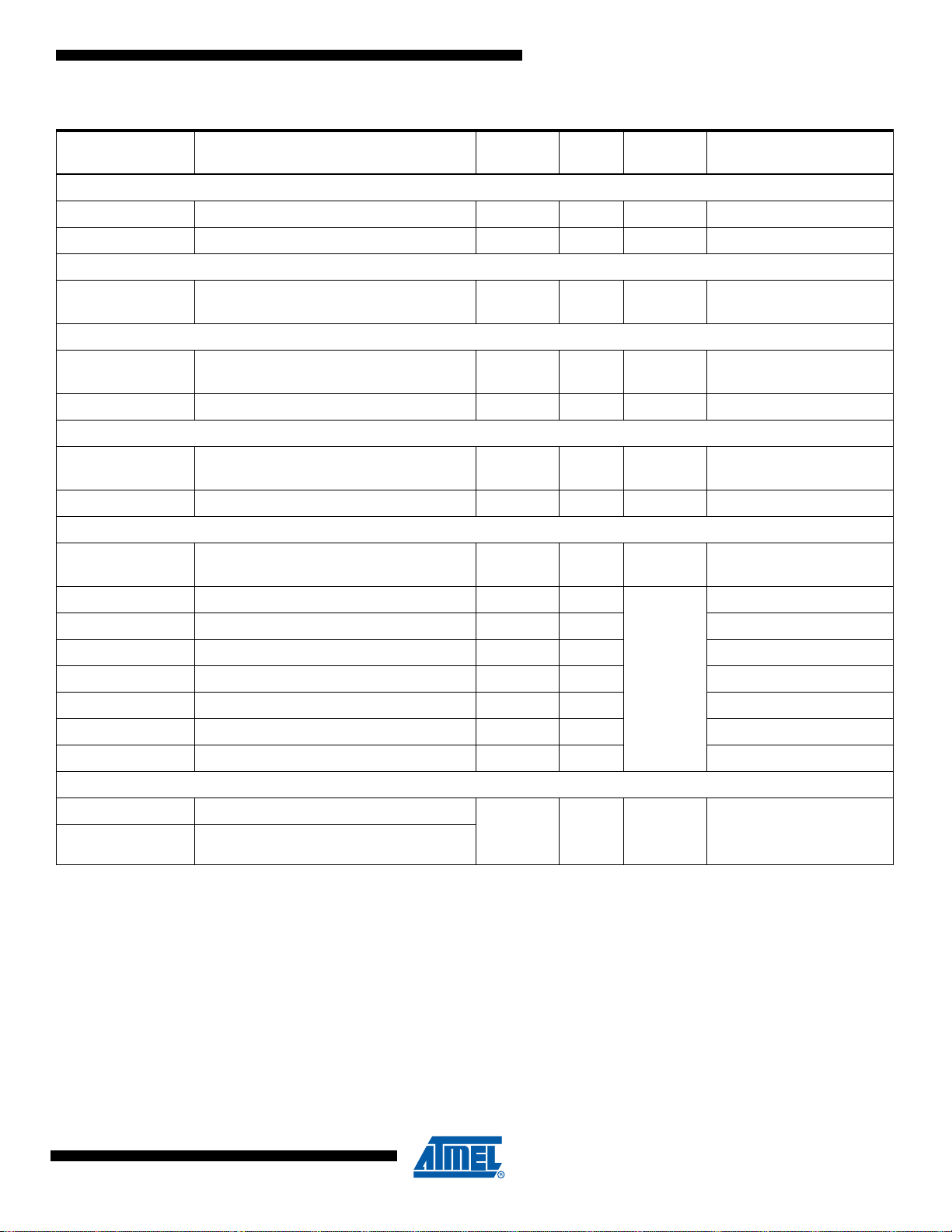
Table 3-1. Signal Description List (Continued)
SAM4S Series [Preliminary]
Active
Signal Name Function Type
Two-Wire Interface- TWI
TWDx TWIx Two-wire Serial Data I/O
TWCKx TWIx Two-wire Serial Clock I/O
Analog
ADVREF
AD0-AD14 Analog Inputs
ADTRG ADC Trigger Input VDDIO
DAC0 - DAC1 Analog output
DACTRG DAC Trigger Input VDDIO
PGMEN0PGMEN2
PGMM0-PGMM3 Programming Mode Input
ADC, DAC and Analog Comparator
Reference
12-bit Analog-to-Digital Converter - ADC
12-bit Digital-to-Analog Converter - DAC
Fast Flash Programming Interface - FFPI
Programming Enabling Input VDDIO
Analog
Analog,
Digital
Analog,
Digital
Level
Voltage
reference Comments
PGMD0-PGMD15 Programming Data I/O
PGMRDY Programming Ready Output High
PGMNV ALID Data Direction Output Low
PGMNOE Programming Read Input Low
PGMCK Programming Clock Input
PGMNCMD Programming Command Input Low
USB Full Speed Device
DDM USB Full Speed Data DDP USB Full Speed Data +
Note: 1. Schmitt Triggers can be disabled through PIO registers.
2. Some PIO lines are shared with System I/Os.
3. Refer to USB Section of the product Electrical Characteristics for information on Pull-down value in USB Mode.
4. See “Typical P owering Schematics” Section for restrictions on voltage range of Analog Cells.
5. TDO pin is set in input mode when the Cortex-M4 Core is not in debug mode. Thus the internal pull-up corresponding to this
PIO line must be enabled to avoid current consumption due to floating input
Analog,
Digital
VDDIO
VDDIO
Reset State:
- USB Mode
- Internal Pull-down
(3)
11100B–ATARM–31-Jul-12
11
4. Package and Pinout
125
26
50
5175
76
100
SAM4S devices are pin-to-pin compatible with SAM3N, SAM3S product s in 64- and 100- pin versions, and AT91SAM7S legacy products in 64-pin versions.
4.1 SAM4SD32/SD16/SA16/S16/S8C Package and Pinout
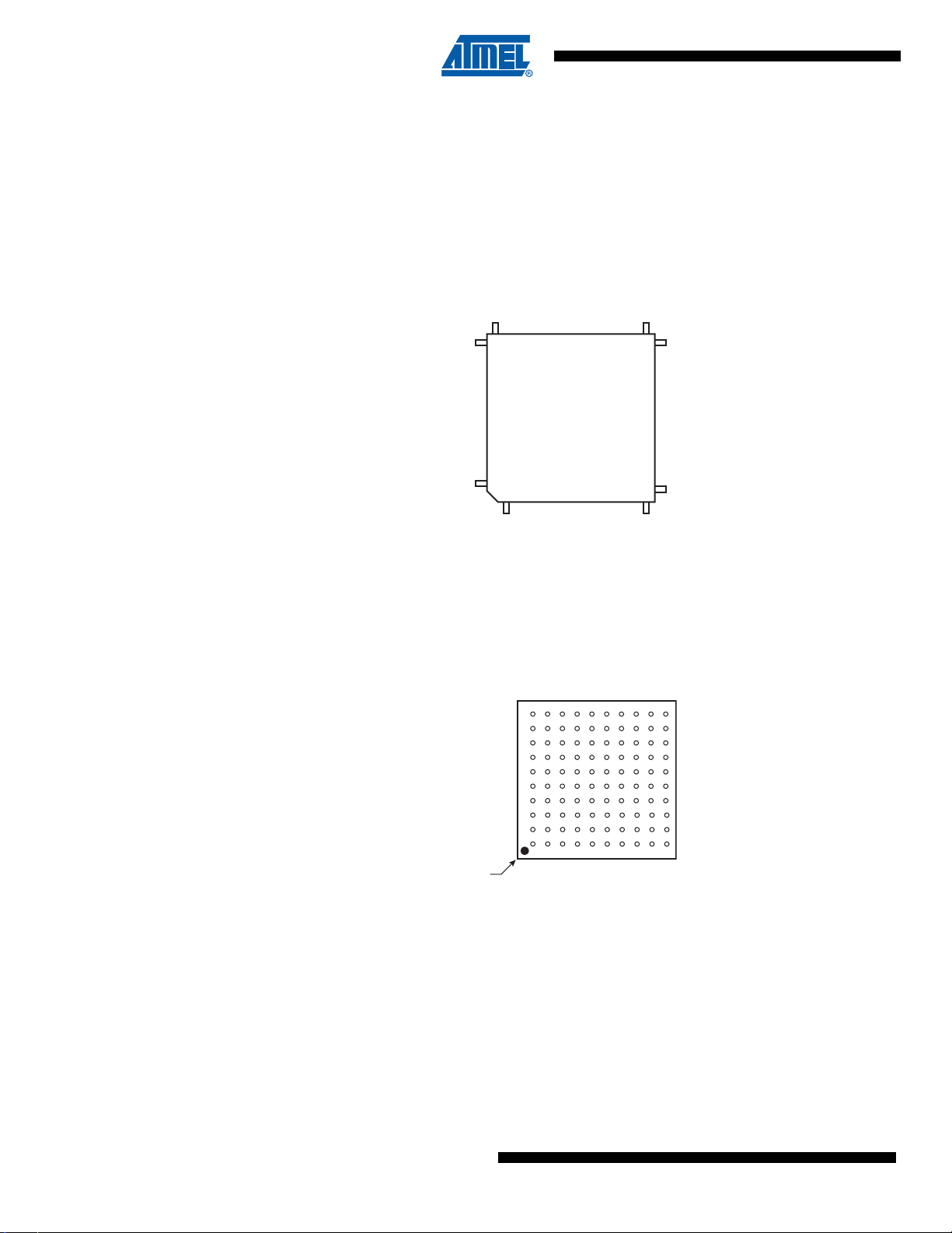
4.1.1 100-Lead LQFP Package Outline
Figure 4-1. Orientation of the 100-lead LQFP Package
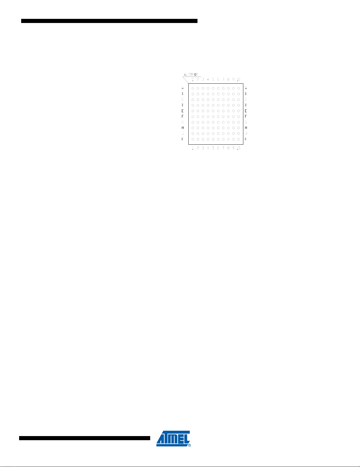
4.1.2 100-ball TFBGA Package Outline
The 100-Ball TFBGA package has a 0.8 mm ball pitch and respects Green Standards. Its
dimensions are 9 x 9 x 1.1 mm. Figure 4-2 shows the orientation of the 100-ball TFBGA
Package.
Figure 4-2. Orientation of the 100-ball TFBGA Package
TOP VIEW
10
9
8
7
6
5
4
3
2
1
BALL A1
ABCDEFGHJK
12
SAM4S Series [Preliminary]
11100B–ATARM–31-Jul-12
4.1.3 100-ball VFBGA Package Outline
Figure 4-3. Orientation of the 100-ball VFBGA Package
SAM4S Series [Preliminary]
11100B–ATARM–31-Jul-12
13
4.1.4 100-Lead LQFP Pinout
Table 4-1. SAM4SD32/SD16/SA16/S16/S8C 100-lead LQFP pinout
1 ADVREF 26 GND 51 TDI/PB4 76
2 GND 27 VDDIO 52 PA6/PGMNOE 77 JTAGSEL
3 PB0/AD4 28 PA16/PGMD4 53 PA5/PGMRDY 78 PC18
4 PC29/AD13 29 PC7 54 PC28 79 TMS/SWDIO/PB6
5 PB1/AD5 30 PA15/PGMD3 55 PA4/PGMNCMD 80 PC19
6 PC30/AD14 31 PA14/PGMD2 56 VDDCORE 81 PA31
7 PB2/AD6 32 PC6 57 PA27/PGMD15 82 PC20
8 PC31 33 PA13/PGMD1 58 PC8 83 TCK/SWCLK/PB7
9 PB3/AD7 34 PA24/PGMD12 59 PA28 84 PC21
10 VDDIN 35 PC5 60 NRST 85 VDDCORE
11 VDDOUT 36 VDDCORE 61 TST 86 PC22
12
13 PC26 38 PA25/PGMD13 63 PA29 88 DDM/PB10
14
15
16 VDDCORE 41 PA12/PGMD0 66 PA3 91 VDDIO
PA17/PGMD5/
AD0
PA18/PGMD6/
AD1
PA21/PGMD9/
AD8
37 PC4 62 PC9 87 ERASE/PB12
39 PA26/PGMD14 64 PA30 89 DDP/PB11
40 PC3 65 PC10 90 PC23
TDO/TRACESWO/
PB5
17 PC27 42 PA11/PGMM3 67 PA2/PGMEN2 92 PC24
18
19 PC15/AD11 44 PA10/PGMM2 69 VDDIO 94 PC25
20
21 PC13/AD10 46 PA9/PGMM1 71 PC14 96 PB8/XOUT
22 PA23/PGMD11 47 PC1 72 PA1/PGMEN1 97 PB9/PGMCK/XIN
23 PC12/AD12 48
24
25 PC0 50 VDDIO 75 PC17 100 VDDPLL
PA19/PGMD7/
AD2
PA22/PGMD10/
AD9
PA20/PGMD8/
AD3
43 PC2 68 PC11 93 PB13/DAC0
45 GND 70 GND 95 GND
49
PA8/XOUT32/
PGMM0
PA7/XIN32/
PGMNVALID
73 PC16 98 VDDIO
74 PA0/PGMEN0 99 PB14/DAC1
14
SAM4S Series [Preliminary]
11100B–ATARM–31-Jul-12
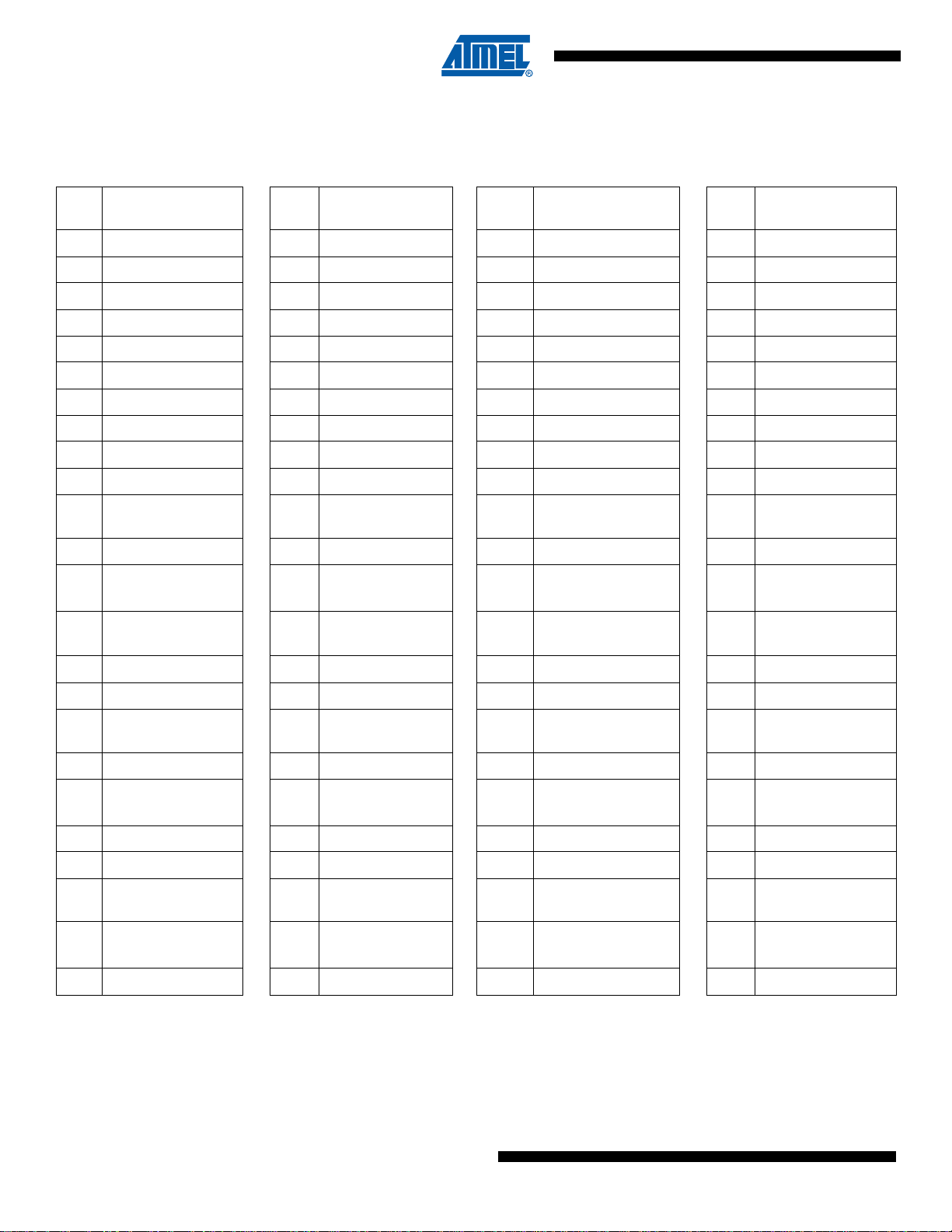
4.1.5 100-Ball TFBGA Pinout
Table 4-2. SAM4SD32/SD16/SA16/S16/S8 100-ball TFBGA pinout
SAM4S Series [Preliminary]
A1 PB1/AD5 C6 TCK/SWCLK/PB7 F1
A2 PC29 C7 PC16 F2 PC26 H7 PA11/PGMM3
A3 VDDIO C8 PA1/PGMEN1 F3 VDDOUT H8 PC1
A4 PB9/PGMCK/XIN C9 PC17 F4 GND H9 PA6/PGMNOE
A5 PB8/XOUT C10 PA0/PGMEN0 F5 VDDIO H10 TDI/PB4
A6 PB13/DAC0 D1 PB3/AD7 F6 PA27/PGMD15 J1 PC15/AD11
A7 DDP/PB11 D2 PB0/AD4 F7 PC8 J2 PC0
A8 DDM/PB10 D3 PC24 F8 PA28 J3 PA16/PGMD4
A9 TMS/SWDIO/PB6 D4 PC22 F9 TST J4 PC6
A10 JTAGSEL D5 GND F10 PC9 J5 PA24/PGMD12
B1 PC30 D6 GND G1 PA21/PGMD9/AD8 J6 PA25/PGMD13
B2 ADVREF D7 VDDCORE G2 PC27 J7 PA10/PGMM2
B3 GNDANA D8 PA2/PGMEN2 G3 PA15/PGMD3 J8 GND
B4 PB14/DAC1 D9 PC11 G4 VDDCORE J9 VDDCORE
B5 PC21 D10 PC14 G5 VDDCORE J10 VDDIO
B6 PC20 E1
PA17/PGMD5/
AD0
G6 PA26/PGMD14 K1
PA18/PGMD6/
AD1
H6 PC4
PA22/PGMD10/
AD9
B7 PA31 E2 PC31 G7 PA12/PGMD0 K2 PC13/AD10
B8 PC19 E3 VDDIN G8 PC28 K3 PC12/AD12
B9 PC18 E4 GND G9 PA4/PGMNCMD K4
B10
TDO/TRACESWO/
PB5
C1 PB2/AD6 E6 NRST H1
C2 VDDPLL E7 PA29/AD13 H2 PA23/PGMD11 K7 PC2
C3 PC25 E8 PA30/AD14 H3 PC7 K8 PA9/PGMM1
C4 PC23 E9 PC10 H4 PA14/PGMD2 K9
C5 ERASE/PB12 E10 PA3 H5 PA13/PGMD1 K10
E5 GND G10 PA5/PGMRDY K5 PC5
PA19/PGMD7/
AD2
K6 PC3
PA20/PGMD8/
AD3
PA8/XOUT32/
PGMM0
PA7/XIN32/
PGMNVALID
11100B–ATARM–31-Jul-12
15
4.1.6 100-Ball VFBGA Pinout
Table 4-3. SAM4SD32/SD16/SA16/S16/S8 100-ball VFBGA pinout
A1 ADVREF C6 PC9 F1 VDDOUT H6 PA12/PGMD0
A2 VDDPLL C7 TMS/SWDIO/PB6 F2
A3 PB9/PGMCK/XIN C8 PA1/PGMEN1 F3
A4 PB8/XOUT C9 PA0/PGMEN0 F4 GND H9 PA6/PGMNOE
A5 JTAGSEL C10 PC16 F5 GND H10
A6 DDP/PB11 D1 PB1/AD5 F6 PC26 J1 PA20/AD3
A7 DDM/PB10 D2 PC30 F7 PA4/PGMNCMD J2 PC12/AD12
A8 PC20 D3 PC31 F8 PA28 J3 PA16/PGMD4
A9 PC19 D4 PC22 F9 TST J4 PC6
PA18/PGMD6/
AD1
PA17/PGMD5/
AD0
H7 PA9/PGMM1
H8 VDDCORE
PA5/PGMRDY
A10
B10 PC17 E5 GND G10 PA27 K5 PA26
TDO/TRACESWO/
PB5
B1 GNDANA D6 PA29/AD13 G1 PC15/AD11 J6 PA25
B2 PC25 D7 PA30/AD14 G2
B3 PB14/DAC1 D8 GND G3 PA21/AD8 J8 VDDCORE
B4 PB13/DAC0 D9 PC14 G4 PA15/PGMD3 J9 VDDCORE
B5 PC23 D10 PC11 G5 PC3 J10 TDI/PB4
B6 PC21 E1 VDDIN G6 PA10/PGMM2 K1 PA23
B7 TCK/SWCLK/PB7 E2 PB3/AD7 G7 PC1 K2 PC0
B8 PA31 E3 PB2/AD6 G8 PC28 K3 PC7
B9 PC18 E4 GND G9 NRST K4 PA13/PGMD1
C1 PB0/AD4 E6 GND H1 PC13/AD10 K6 PC2
C2 PC29 E7 VDDIO H2 PA22/AD9 K7 VDDIO
C3 PC24 E8 PC10 H3 PC27 K8 VDDIO
C4 ERASE/PB12 E9 PA2/PGMEN2 H4 PA14/PGMD2 K9
C5 VDDCORE E10 PA3 H5 PC4 K10
D5 PC5 F10 PC8 J5 PA24
PA19/PGMD7/
AD2
J7 PA11/PGMM3
PA8/XOUT32/
PGMM0
PA7/XIN32/
PGMNVALID
16
SAM4S Series [Preliminary]
11100B–ATARM–31-Jul-12
SAM4S Series [Preliminary]
33
49
48
32
17
16
1
64
4.2 SAM4SD32/SD16/SA16/S16/S8 Package and Pinout
4.2.1 64-Lead LQFP Package Outl ine
Figure 4-4. Orientation of the 64-lead LQFP Package
4.2.2 64-lead QFN Package Outline
Figure 4-5. Orientation of the 64-lead QFN Package
16
4964
1
17
TOP VIEW
48
33
32
11100B–ATARM–31-Jul-12
17
4.2.3 64-Lead LQFP and QFN Pinout
Table 4-4. 64-pin SAM4SD32/SD16/SA16/S16/S8 pinout
1 ADVREF 17 GND 33 TDI/PB4 49
2 GND 18 VDDIO 34 PA6/PGMNOE 50 JTAGSEL
3 PB0/AD4 19 PA16/PGMD4 35 PA5/PGMRDY 51 TMS/SWDIO/PB6
4 PB1/AD5 20 PA15/PGMD3 36 PA4/PGMNCMD 52 PA31
5 PB2/AD6 21 PA14/PGMD2 37 PA27/PGMD15 53 TCK/SWCLK/PB7
6 PB3/AD7 22 PA13/PGMD1 38 PA28 54 VDDCORE
7 VDDIN 23 PA24/PGMD12 39 NRST 55 ERASE/PB12
8 VDDOUT 24 VDDCORE 40 TST 56 DDM/PB10
9
10
11
12 VDDCORE 28 PA11/PGMM3 44 PA2/PGMEN2 60 GND
13
14
PA17/PGMD5/
AD0
PA18/PGMD6/
AD1
PA21/PGMD9/
AD8
PA19/PGMD7/
AD2
PA22/PGMD10/
AD9
25 PA25/PGMD13 41 PA29 57 DDP/PB11
26 PA26/PGMD14 42 PA30 58 VDDIO
27 PA12/PGMD0 43 PA3 59 PB13/DAC0
29 PA10/PGMM2 45 VDDIO 61 XOUT/PB8
30 PA9/PGMM1 46 GND 62 XIN/PGMCK/PB9
TDO/TRACESWO/
PB5
15 PA23/PGMD11 31
16
Note: The bottom pad of the QFN package must be connected to ground.
PA20/PGMD8/
AD3
32
PA8/XOUT32/
PGMM0
PA7/XIN32/
PGMNVALID
47 PA1/PGMEN1 63 PB14/DAC1
48 PA0/PGMEN0 64 VDDPLL
18
SAM4S Series [Preliminary]
11100B–ATARM–31-Jul-12

5. Power Considerations
5.1 Po wer Supplies
The SAM4S has several types of power supply pins:
• VDDCORE pins: Power the core, the embedded memories and the peripherals. Voltage
ranges from 1.08V to 1.32V.
• VDDIO pins: Powe r the Peripherals I/ O lines (Input/ Output Buffers), USB tra nsceiv er, Bac kup
part, 32 kHz crystal oscillator and oscillator pads. Voltage ranges from 1.62V to 3.6V.
• VDDIN pin: Voltage Regulator Input, ADC, DAC and Analog Comparator Power Supply.
Voltage ranges from 1.62V to 3.6V.
• VDDPLL pin: Powers the PLLA, PLLB, the Fast RC and the 3 to 20 MHz oscillator. Voltage
ranges from 1.08V to 1.32V.
5.2 Voltage Regulator
The SAM4S embeds a voltage regulator that is managed by the Supply Controller.
This internal regulator is designed to supply the internal cor e of SAM4S It fe atures two o perat ing
modes:
SAM4S Series [Preliminary]
• In Normal mode, the voltage regulator consumes less than 500 µA static current and draws
80 mA of output current. Internal adaptive biasing adjusts the regulator quiescent current
depending on the required load current. In Wait Mode quiescent current is only 5 µA.
• In Backup mod e, the v oltage r egulator consumes less t han 1µA while its output (VDDOUT) is
driven internally to GND. The default output voltage is 1.20V and the start-up time to reach
Normal mode is less than 300 µs.
For adequate input and output power supply d ecoupling/bypassing , refer to the “ Voltage Regulator” section in the “Electrical Characteristics” section of the datasheet.
5.3 Typical Powering Schematics
The SAM4S supports a 1.62V-3.6V single supply mode. The internal regulator input is connected to the source and its output feeds VDDCORE. Figure 5-1 below shows the power
schematics.
As VDDIN powers the voltage regulator, the ADC, DAC and the analog comparator, when the
user does not want to use the embedded voltage regulator, it can be disabled by software via
the SUPC (note that this is different from Backup mode).
11100B–ATARM–31-Jul-12
19
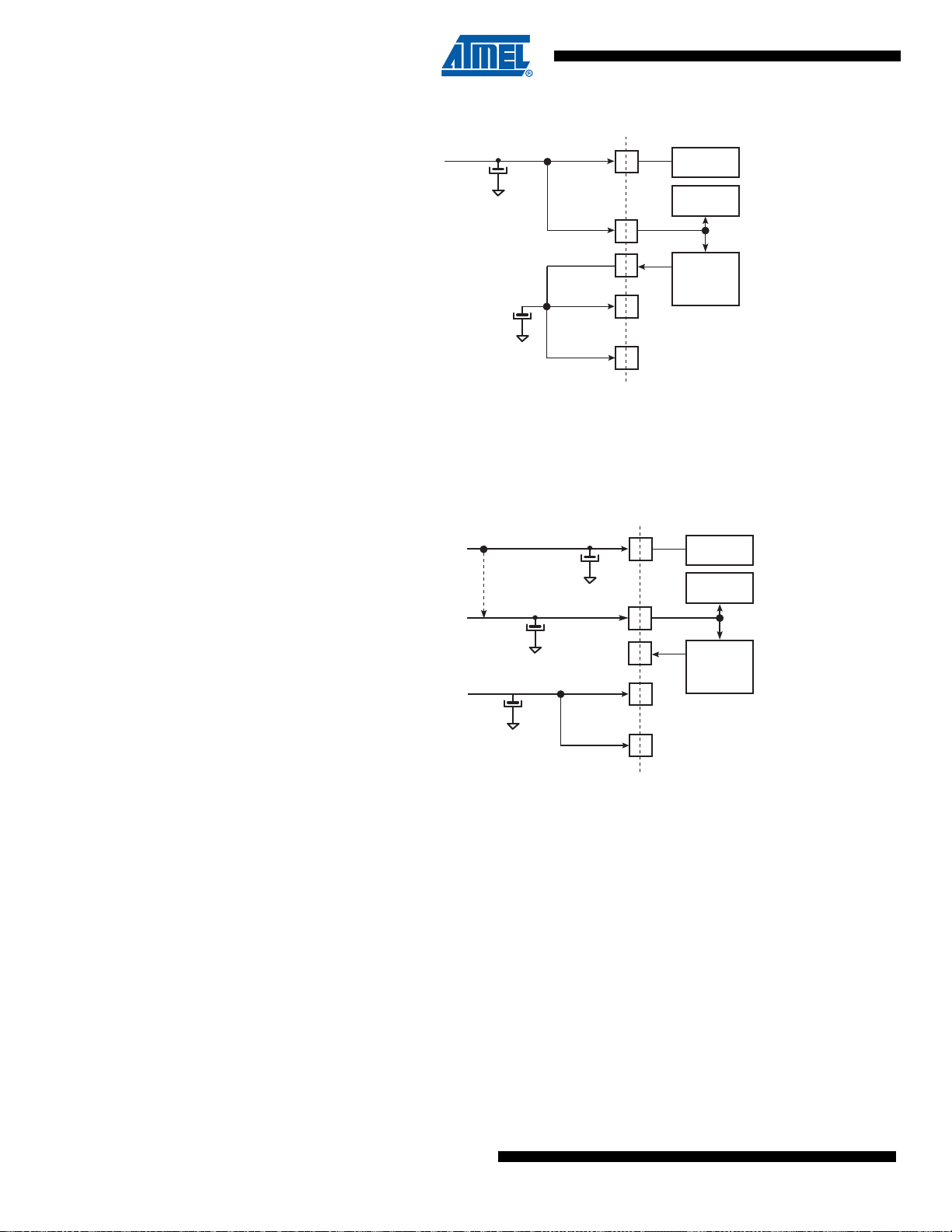
Figure 5-1. Single Supply
Main Supply
(1.62V-3.6V)
ADC, DAC
Analog Comp.
USB
Transceivers.
VDDIN
Voltage
Regulator
VDDOUT
VDDCORE
VDDIO
VDDPLL
Note: Restrictions
For USB, VDDIO needs to be greater than 3.0V.
For ADC, VDDIN needs to be greater than 2.0V.
For DAC, VDDIN needs to be greater than 2.4V.
Figure 5-2. Core Externally Supplied
Main Supply
(1.62V-3.6V)
Can be the
same supply
ADC, DAC, Analog
Comparator Supply
(2.0V-3.6V)
VDDCORE Supply
(1.08V-1.32V)
VDDIO
VDDIN
VDDOUT
VDDCORE
USB
Transceivers.
ADC, DAC
Analog Comp.
Voltage
Regulator
20
Note: Restrictions
For USB, VDDIO needs to be greater than 3.0V.
For ADC, VDDIN needs to be greater than 2.0V.
For DAC, VDDIN needs to be greater than 2.4V.
Figure 5-3 below provides an example of the powering scheme when using a backu p battery.
Since the PIO state is preserved when in backup mode, any free PIO line can be used to switch
off the external regulator by driving the PIO line at low level (PIO is input, pull-up enabled after
backup reset). External wake-up of the system can be from a push button or any signal. See
Section 5.6 “Wake-up Sources” for further details.
SAM4S Series [Preliminary]
VDDPLL
11100B–ATARM–31-Jul-12
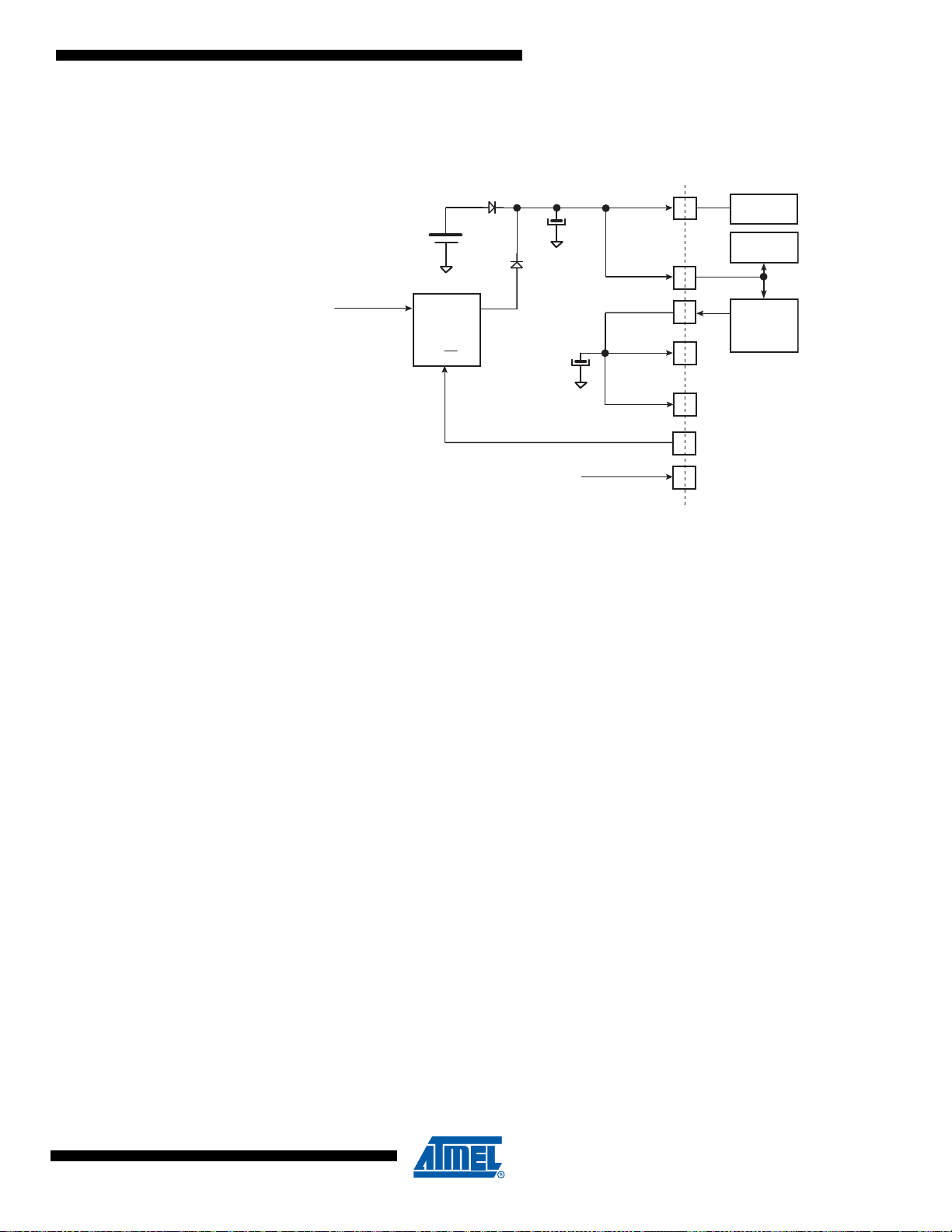
Figure 5-3. Backup Battery
ADC, DAC
Analog Comp.
USB
Transceivers.
VDDIN
Voltage
Regulator
3.3V
LDO
Backup
Battery
+
-
ON/OFF
IN
OUT
VDDOUT
Main Supply
VDDCORE
ADC, DAC, Analog
Comparator Supply
(2.0V-3.6V)
VDDIO
VDDPLL
PIOx (Output)
WAKEUPx
External wakeup signal
Note: The two diodes provide a “switchover circuit” (for illustration purpose)
between the backup battery and the main supply when the system is put in
backup mode.
SAM4S Series [Preliminary]
5.4 Active Mode
5.5 Low-power Modes
5.5.1 Backup Mode
Active mode is the normal running mode with the core clock running from the fast RC oscillator,
the main crystal oscillator or the PLLA. The power management controller can be used to adapt
the frequency and to disable the peripheral clocks.
The various low-power modes of the SAM4S are described below:
The purpose of backup mode is to achieve the lowest power consumption possible in a system
which is performing periodic wake-ups to perform tasks but not requiring fast startup time. Total
current consumption is 1 µA typical (VDDIO = 1.8 V to 25°).
The Supply Controller, zero-power power-on reset, RTT, RTC, Backup registers and 32 kHz
oscillator (RC or crystal oscillator selected by software in the Supply Controller) are running. The
regulator and the core supply are off.
Backup mode is based on the Cortex-M4 deep sleep mode with the voltage regula tor disabled.
The SAM4S can be awakened f rom th is m o de through WUP0-15 pins, the su pp ly m o nit or ( SM) ,
the RTT or RTC wake-up event.
Backup mode is entered by writing the Supply Controller Control Register (SUPC_CR) with the
VROFF bit at 1 (A key is needed to write t he VR OF F bi t, plea se ref er t o Supp ly Contr oller SUPC
section of the product datasheet) and with the SLEEPDEEP bit in the Cortex-M4 System Control
Register set to 1. (See the Power management description in The ARM Cortex-M4 Processor
section of the product datasheet).
11100B–ATARM–31-Jul-12
21

5.5.2 Wait Mode
Entering Backup mode:
• Set the SLEEPDEEP bit of Cortex_M4 to 1
• Set the VR OFF bit of SUPC_CR to 1
Exit from Backup mode happens if one of the following enable wake up events occurs:
• WKUPEN0-15 pins (level transition, configurable debouncing)
• Supply Monitor alarm
•RTC alarm
• RTT alarm
The purpose of the wait mode is to achieve ve ry low power consumption while maintainin g the
whole device in a powered state for a startup time of less than 10 µs. Current Consumption in
Wait mode is typically 32 µA (total current consumption) if the internal voltage regulator is used.
In this mode, the clocks of the core, peripherals and memories are stopped. However, the core,
peripherals and memories power supplies are still powered. From this mode, a fast start up is
available.
This mode is entered by setting WAITMODE bit to 1 (in PMC clock generator Main Oscillator
register) with LPM = 1 (Low Power Mode bit in PMC_FSMR) and with FLPM = 00 or FLPM=01
(Flash Low Power Mode bits in PMC_FSMR).
The Cortex-M4 is able to handle external events or internal events in order to wake-up the core.
This is done by configuring the external lines WUP0-15 as fast startup wake-up pins (refer to
Section 5.7 “Fast Startup”). RTC or RTT Alarm and USB wake-up events can be used to wake
up the CPU.
Entering Wait Mode:
• Select the 4/8/12 MHz fast RC oscillator as Main Clock
• Set the LPM bit in the PMC Fast Startup Mode Register (PMC_FSMR)
• Set the FLPM bitfield in the PMC Fast Startup Mode Register (PMC_FSMR)
• Set Flash Wait State at 0.
• Set the WAITMODE bit = 1 in PMC Main Oscillator Register (CKGR_MOR)
• Wait for Master Clock Ready MCKRDY = 1 in the PMC Status Register (PMC_SR)
Note: Internal Main clock resynchronization cycles are necessary between the writing of MOSCRCEN
bit and the effective entry in Wait mode. Depending on the user application, waiting for
MOSCRCEN bit to be cleared is recommended to ensure that the core will not execute undesired
instructions.
Depending on Flash Low Power Mode (FLPM) value, the Flash will enter in three different
modes:
• FLPM[00] in Standby mode
• FLPM[01] in Deep Power Down mode
• FLPM[10] in Idle mode.
Following the Flash mode selection, the consumption in wait mode will decrease. In Deep Power
22
Down mode the recovery time of the Flash in Standby mode will be less than the power up
delay.
SAM4S Series [Preliminary]
11100B–ATARM–31-Jul-12

SAM4S Series [Preliminary]
5.5.3 Sleep Mode
The purpose of sleep mode is to optimize power consumption of the device versus response
time. In this mode, only the core clock is stopped. The peripheral clocks can be enabled. The
current consumption in this mode is application dependent.
This mode is entered via Wait for Interrupt (WFI) instructions with LPM = 0 in PMC_FSMR.
The processor can be awakened from an interrupt if WFI instruction of the Cortex-M4 is used.
5.5.4 Low Power Mode Summary Table
The modes detailed above are the main low-power modes. Each part can be set to on or off separately and wake up sources can be individually configured. Table 5-1 below shows a summary
of the configurations of the low-power modes.
Table 5-1. Low-power Mode Configuration Summary
SUPC,
32 kHz Osc,
RTC, RTT
Backup
Registers,
POR
(Backup
Mode
Backup
Mode
Wait
Mode
w/Flash
in
Standby
mode
Wait
Mode
w/Flash
in Deep
Power
Down
mode
Sleep
Mode
Region) Regulator
ON OFF
ON ON
ON ON
ON ON
Notes: 1. The external loads on PIOs are not taken into account in the calculation.
2. Supply Monitor current consumption is not included.
3. When considering wake-up time, the time required to start the PLL is not taken into account. Once started, the device works
with the 4/8/12 MHz fast RC oscillator. The user has to add the PLL start-up time if it is needed in the system. The wake-up
time is defined as the time taken for wake up until the first instruction is fetched.
4. Total consumption 1 µA typ to 1.8V on VDDIO to 25°C.
5. 20.4 µA on VDDCORE, 32.2 µA for total current consumption.
6. Depends on MCK frequency.
7. Depends on MCK frequency. In this mode, the core is supplied but some peripherals can be clocked.
Core
Memory
Peripherals Mode Entry
OFF
(Not powered)
Powered
(Not clocked)
Powered
(Not clocked)
Powered
(Not clocked)
VROFF bit = 1
+SLEEPDEEP
bit = 1
WAITMODE bit
=1
+SLEEPDEEP
bit = 0
+LPM bit = 1
FLPM0 bit = 0
FLPM1 bit = 0
WAITMODE bit
=1
+SLEEPDEEP
bit = 0
+LPM bit = 1
FLPM0 bit = 0
FLPM1 bit = 1
WFI
(6)
+SLEEPDEEP
bit = 0
+LPM bit = 0
Potential Wake Up
Sources
WUP0-15 pins
SM alarm
RTC alarm
RTT alarm
Any Event from:
Fast startup through
WUP0-15 pins
RTC alarm
RTT alarm
USB wake-up
Any Event from:
Fast startup through
WUP0-15 pins
RTC alarm
RTT alarm
USB wake-up
Entry mode =WFI
Interrupt Only;
Any Enabled
Interrupt
Core at
Wake Up
Reset
Clocked
back
Clocked
back
Clocked
back
PIO State
while in Low
Power Mode
Previous
state saved
Previous
state saved
Previous
state saved
Previous
state saved
PIO State
at Wake Up
PIOA &
PIOB &
PIOC
Inputs with
pull ups
Unchanged 32.2 µA
Unchanged 27.6 µA < 10µs
Unchanged
Consumption
(1) (2)
1 µA typ
(7) (7)
Wake-up
Time
(4)
300 ms
(5)
< 10 µs
(3)
11100B–ATARM–31-Jul-12
23
5.6 Wake-up Sour ces
WKUP15
WKUPEN15
WKUPT15
WKUPEN1
WKUPEN0
Debouncer
SLCK
WKUPDBC
WKUPS
RTCEN
rtc_alarm
SMEN
sm_out
Core
Supply
Restart
WKUPIS0
WKUPIS1
WKUPIS15
Falling/Rising
Edge
Detector
WKUPT0
Falling/Rising
Edge
Detector
WKUPT1
Falling/Rising
Edge
Detector
WKUP0
WKUP1
RTTEN
rtt_alarm
The wake-up events allow the device to exit the backup mode. When a wake-up event is
detected, the Supply Controller performs a sequence which automatically reenables the core
power supply and the SRAM power supply, if they are not already enabled.
Figure 5-4. Wake-up Source
24
SAM4S Series [Preliminary]
11100B–ATARM–31-Jul-12
5.7 Fast Startup
SAM4S Series [Preliminary]
The SAM4S allows the processor to restart in a few microseconds while the processor is in wait
mode or in sleep mode. A fast start up can occur upon detection of a low level on one of the 19
wake-up inputs (WKUP0 to 15 + SM + RTC + RTT).
The fast restart circuitry, as shown in Figure 5-5, is fully asynchronous and provides a fast startup signal to the Power Management Controller. As soon as the fast start-up signal is asserted,
the PMC automatically restarts the embedded 4/8/12 MHz Fast RC oscillator, switches the master clock on this 4 MHz clock and reenables the processor clock.
Figure 5-5. Fast Start-Up Sources
FSTT0
WKUP0
WKUP1
WKUP15
FSTP0
FSTP1
FSTP15
RTT Alarm
RTC Alarm
USB Alarm
FSTT1
FSTT15
fast_restart
RTTAL
RTCAL
USBAL
11100B–ATARM–31-Jul-12
25
6. Input/Output Lines
The SAM4S has several kinds of input/o utput (I/O) lines such as general pur pose I/Os (GPIO)
and system I/Os. GPIOs can have alternate functionality due to multiplexing capabilities of the
PIO controllers. The same PIO line can be used whether in I/O mode or by the multiplexed
peripheral. System I/Os include pins such as test pins, oscillators, erase or analog inputs.
6.1 General Purpose I/O Lines
GPIO Lines are managed by PIO Controllers. All I/Os have several input or output modes such
as pull-up or pull-down, input Schmitt triggers, multi-drive (open-drain), glitch filters, debouncing
or input change interrupt. Programming of these modes is performed independently for each I/O
line through the PIO controller user inte rface. F or mo re det ails, refe r to the p roduct “ PIO Contr oller” section.
The input/output buffers of the PIO lines are supplied through VDDIO power supply rail.
The SAM4S embeds high speed pads able to handle up to 7 0 MHz for HSMCI ( MCK/2), 7 0 MHz
for SPI clock lines and 46 MHz on other lines. See the “AC Characteristics” sub-section of the
product Electrical Characteristics. Typical pull-up and pull-down value is 100 kΩ for all I/Os.
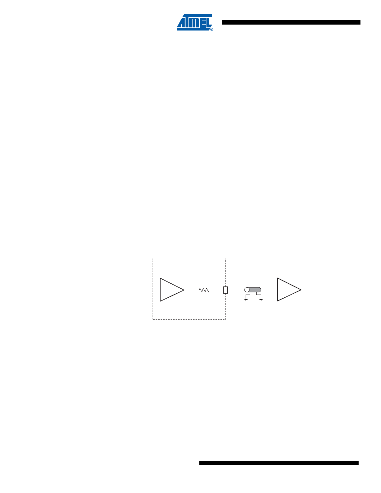
Each I/O line also embeds an ODT (On-Die Termination), (see Figure 6-1 below). It consists of
an internal series resistor termination scheme for impedance matching between the driver output (SAM4S) and the PCB trace impedance preventing signal reflection. The series resistor
helps to reduce IOs switching current (di/dt) thereby reducing in turn, EMI. It also decreases
overshoot and undershoot (ringing) due to inductance of interconnect between devices or
between boards. In conclusion ODT helps diminish signal integrity issues.
Figure 6-1. On-Die Termination
6.2 System I/O Lines
System I/O lines are pins used by oscillators, test mode, reset and JTAG to name but a few.
Described below in Table 6-1are the SAM4S system I/O lines shared with PIO lines.
These pins are software configurable as general purpose I/O or system pins. At startup the
default function of these pins is always used.
SAM4 Driver with
Zout ~ 10 Ohms
Z0 ~ Zout + Rodt
ODT
36 Ohms Typ.
Rodt
Receiver
PCB T race
Z0 ~ 50 Ohms
26
SAM4S Series [Preliminary]
11100B–ATARM–31-Jul-12
Table 6-1. System I/O Configuration Pin List.
SAM4S Series [Preliminary]
SYSTEM_IO
bit number
12 ERASE PB12 Low Level at startup
10 DDM PB10 11 DDP PB11 -
7 TCK/SWCLK PB7 6 TMS/SWDIO PB6 5 TDO/TRACESWO PB5 4 TDI PB4 -
- PA7 XIN32 -
- PA8 XOUT32 -
- PB9 XIN -
- PB8 XOUT -
Notes: 1. If PB12 is used as PIO input in user applications, a low level must be ensured at startup to prevent Flash erase before the
user application sets PB12 into PIO mode,
2. In the product Datasheet Refer to: “Slow Clock Generator” of the “Supply Controller” section.
3. In the product Datasheet Refer to: “3 to 20 MHZ Crystal Oscillator” information in the “PMC” section.
Default function
after reset Other function
Constraints for
normal start Configuration
(1)
In Matrix User Interface Registers
(Refer to the System I/O
Configuration Register in the “Bus
Matrix” section of the datasheet.)
See footnote
See footnote
(2)
below
(3)
below
6.2.1 Serial Wire JTAG Debug Port (SWJ-DP) Pins
The SWJ-DP pins are TCK/SWCLK, TMS/SWDIO, TDO/SWO, TDI and commonly provided on
a standard 20-pin JTAG connector defined by ARM. For more details about voltage reference
and reset state, refer to Table 3-1 on page 8.
At startup, SWJ-DP pins are configured in SWJ-DP mode to allow connection with debugging
probe. Please refer to the “Debug and Test” Section of the product datasheet.
SWJ-DP pins can be used as standard I/Os to provide users more gene ral input/output pins
when the debug port is not needed in the end application. Mode selection between SWJ-DP
mode (System IO mode) and general IO mode is performed through the AHB Matrix Special
Function Registers (MATRIX_SFR). Configuration of the pad for pull-up, triggers, debouncing
and glitch filters is possible regardless of the mode.
The JTAGSEL pin is used to select the JTAG boundary scan when asserted at a high level. It
integrates a permanent pull-do wn resistor of ab out 15 kΩ to GND, so that it can be left unconnected for normal operations.
By default, the JTAG Debug Port is active. If the debugger host wants to switch to the Serial
Wire Debug Port, it must provide a dedicated JTAG sequence on TMS/SWDIO and
TCK/SWCLK which disables the JTAG-DP and enables the SW-DP. When the Serial Wire
Debug Port is active, TDO/TRACESWO can be used for trace.
The asynchronous TRACE output (TRACESWO) is multiplexed with TDO. So the asynchrono us
trace can only be used with SW-DP, not JTAG-DP. For more information about SW-DP and
JTAG-DP switching, please refer to the “Debug and Test” Section.
11100B–ATARM–31-Jul-12
27

6.3 Test Pin
6.4 NRST Pin
6.5 ERASE Pin
The TST pin is used for JTAG Boundary Scan Manuf acturing Test or Fast Fl ash programming
mode of the SAM4S series. The TST pin integrates a permanent pull-down resistor of about 15
kΩ to GND, so that it can be left unconnected for normal operations. To enter fast programming
mode, see the Fast Flash Programming Interface (FFPI) sectio n. For more on t he manufact uring
and test mode, refer to the “Debug and Test” section of the product datasheet.
The NRST pin is bidirectional. It is handled by the on-chip r eset controller and can be driven low
to provide a reset signal to the external components or asserted low ex ternally to reset the
microcontroller. It will reset the Core and the peripherals except the Backup region (RTC, RTT
and Supply Controller). There is no constraint on t he leng th of t he r eset p ulse and t he re set controller can guarantee a minimum pulse length. The NRST pin integrates a permanent pull-up
resistor to VDDIO of about 100 kΩ. By default, the NRST pin is configured as an input.
The ERASE pin is used to reinitialize the Flash content (and some of its NVM bits) to an erased
state (all bits read as logic level 1). It inte gra tes a pull-down resistor of about 100 kΩ to GND, so
that it can be left unconnected for normal operations.
This pin is debounced by SCLK to improve the glitch toleran ce. When the ERASE pin is tied high
during less than 100 ms, it is not taken into account. The pin mu st be tied high during more than
220 ms to perform a Flash erase operation.
The ERASE pin is a system I/O pin and can be used as a standard I/O. At startup, the ERASE
pin is not configured as a PIO pin. If the ERASE pin is used as a standard I/O, startup level of
this pin must be low to prevent unwanted erasing. Refer to Section 10.2 “Peripheral Signal Mul-
tiplexing on I/O Lines” on page 40. Also, if the ERASE pin is used as a standard I/O output,
asserting the pin to low does not erase the Flash.
28
SAM4S Series [Preliminary]
11100B–ATARM–31-Jul-12
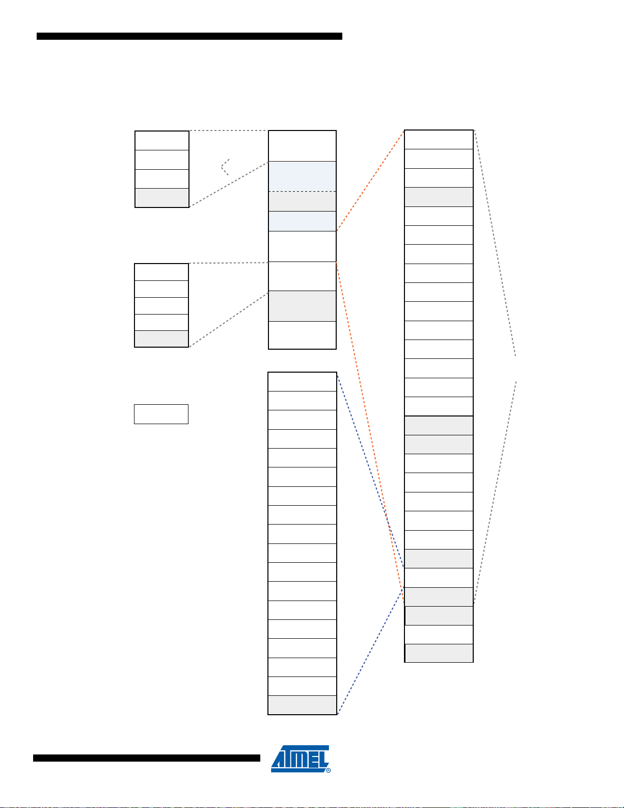
7. Product Mapping
Address memory space
Code
1 MByte
bit band
regiion
1 MByte
bit band
regiion
1 MByte
bit band
regiion
0x00000000
SRAM
0x20000000
0x20100000
0x20400000
0x24000000
0x40000000
offset
ID
peripheral
block
Code
Boot Memory
0x00000000
0x00400000
0x00800000
Reserved
0x00C00000
0x1FFFFFFF
Peripherals
HSMCI
18
0x40000000
SSC
22
0x40004000
SPI
21
0x40008000
0x4000C000
TC0
TC0
0x40010000
23
TC0
TC1
+0x40
24
TC0
TC2
+0x80
25
TC1
TC3
0x40014000
26
TC1
TC4
+0x40
27
TC1
TC5
+0x80
28
TWI0
19
0x40018000
TWI1
20
0x4001C000
PWM
31
0x40020000
USART0
USART1
14
0x40024000
15
0x40028000
0x4002C000
Reserved
Reserved
0x40030000
UDP
33
0x40034000
ADC
29
0x40038000
DACC
30
0x4003C000
ACC
34
0x40040000
CRCCU
35
0x40044000
0x40048000
System Controller
0x400E0000
0x400E2600
0x40100000
0x40200000
0x40400000
0x60000000
External RAM
SMC Chip Select 0
0x60000000
SMC Chip Select 1
Undefined
32 MBytes
bit band alias
0x61000000
SMC Chip Select 2
0x62000000
SMC Chip Select 3
0x63000000
0x64000000
0x9FFFFFFF
System Controller
SMC
10
0x400E0000
MATRIX
0x400E0200
PMC
5
0x400E0400
UART0
UART1
8
0x400E0600
CHIPID
0x400E0740
9
0x400E0800
EFC
6
0x400E0A00
0x400E0C00
PIOA
11
0x400E0E00
PIOB
12
0x400E1000
PIOC
13
0x400E1200
RSTC
0x400E1400
1
SUPC
+0x10
RTT
+0x30
3
WDT
+0x50
4
RTC
+0x60
2
GPBR
+0x90
0x400E1600
0x4007FFFF
Internal Flash
Internal ROM
Reserved
Peripherals
External SRAM
0x60000000
0xA0000000
System
0xE0000000
0xFFFFFFFF
Reserved
Reserved
EFC1
Reserved
Reserved
Reserved
Reserved
32 MBytes
bit band alias
Reserved
Figure 7-1. SAM4S Product Mapping
SAM4S Series [Preliminary]
11100B–ATARM–31-Jul-12
29

8. Memories
8.1 Embedded Memories
8.1.1 Internal SRAM
The SAM4SD32 device (2x1024 Kbytes) embeds a total of 160-Kbytes high-speed SRAM.
The SAM4SD16 device (2x512KBytes)embeds a total of 160-Kbytes high-speed SRAM.
The SAM4SA16 device (1024 Kbytes) embeds a total of 160 -Kb yt es hig h -spe ed SRAM.
The SAM4S16 device (1024 Kbytes) embeds a total of 128-Kbytes high-speed SRAM.
The SAM4S8 device (512 Kbytes) embeds a total of 128-Kbytes high-speed SRAM.
The SRAM is accessible over System Cortex-M4 bus at address 0x2000 0000.
The SRAM is in the bit band region. The bit band alias region is from 0x2200 0000 to
0x23FF FFFF.
8.1.2 Internal ROM
The SAM4S embeds an Internal ROM, which contains the SAM Boot Assistant (SAM-BA
Application Programming routines (IAP) and Fast Flash Programming Interface (FFPI).
At any time, the ROM is mapped at address 0x0080 0000.
8.1.3 Embedded Flash
8.1.3.1 Flash Overview
The memory is organized in sectors. Each sector has a size of 64 KBytes. The first sector of 64
KBytes is divided into 3 smaller sectors.
The three smaller sectors are organized to consist of 2 sectors of 8 KBytes and 1 sector of 48
KBytes. Refer to Figure 8-1, "Global Flash Organization" below.
®
), In
30
SAM4S Series [Preliminary]
11100B–ATARM–31-Jul-12
 Loading...