

Page 1

SAM3N-EK Development Board
....................................................................................................................
User Guide
11080C–ATARM–30-Mar-11
Page 2

Section 1
Introduction.................................................................................................................1-1
1.1 SAM3N Evaluation Kit........................................................................................................ 1-1
1.2 User Guide ......................................................................................................................... 1-1
1.3 References and Applicable Documents ............................................................................. 1-1
Section 2
Kit Contents ................................................................................................................2-1
2.1 Deliverables ....................................................................................................................... 2-1
2.2 Electrostatic Warning ......................................................................................................... 2-2
Section 3
Power Up....................................................................................................................3-1
3.1 Power up the Board ...........................................................................................................3-1
3.2 DevStart ............................................................................................................................. 3-1
3.3 Recovery Procedure .......................................................................................................... 3-1
3.4 Sample Code and Technical Support ................................................................................ 3-1
Section 4
Evaluation Kit Hardware .............................................................................................4-1
4.1 Board Overview.................................................................................................................. 4-1
4.2 Features List ...................................................................................................................... 4-2
4.3 Function Blocks.................................................................................................................. 4-2
4.3.1 Processor............................................................................................................. 4-2
4.3.2 Memory................................................................................................................ 4-2
4.3.3 Clock Circuitry...................................................................................................... 4-3
4.3.4 Reset Circuitry ..................................................................................................... 4-3
4.3.5 Power Supply and Management.......................................................................... 4-4
4.3.6 UART ................................................................................................................... 4-4
4.3.7 Display Interface .................................................................................................. 4-5
4.3.8 Backlight Control.................................................................................................. 4-5
4.3.9 JTAG/ICE............................................................................................................. 4-6
4.3.10 PWM Buzzer ........................................................................................................ 4-6
4.3.11 SD/MMC Card ..................................................................................................... 4-6
4.3.12 Touch Elements .................................................................................................. 4-7
4.3.13 User Buttons ........................................................................................................ 4-7
4.3.14 LEDs .................................................................................................................... 4-8
4.3.15 ZigBee ................................................................................................................. 4-8
4.3.16 PIO Expansion ..................................................................................................... 4-8
4.4 Configuration...................................................................................................................... 4-9
4.4.1 PIO Usage ........................................................................................................... 4-9
SAM3N-EK Development Board User Guide 1-1
11080C–ATARM–30-Mar-11
Page 3

4.4.2 Jumpers ............................................................................................................. 4-12
4.4.3 Test Points ......................................................................................................... 4-12
4.4.4 Assigned PIO Lines, Disconnection Possibility.................................................. 4-13
Section 5
QT600.........................................................................................................................5-1
5.1 Overview ............................................................................................................................ 5-1
5.2 System Description ............................................................................................................ 5-2
5.3 Features ............................................................................................................................. 5-2
5.4 Getting Started ................................................................................................................... 5-3
5.5 Hardware Description.........................................................................................................5-5
5.5.1 QT600 Interface Board ........................................................................................ 5-5
5.5.2 TOUCH DATA Connectors .................................................................................. 5-7
5.5.3 Target Voltage VTG ............................................................................................. 5-8
5.5.4 VTG LED ............................................................................................................. 5-8
5.5.5 TOUCH DATA LED ............................................................................................. 5-8
5.5.6 STATUS LED....................................................................................................... 5-9
5.5.7 Touch ATx Firmware ........................................................................................... 5-9
5.6 Touch Debug...................................................................................................................... 5-9
5.7 Using QT600 and AVR QTouch Studio for Custom Applications....................................... 5-9
5.8 Troubleshooting and Support........................................................................................... 5-10
5.8.1 Technical Support .............................................................................................. 5-10
5.8.2 Force Firmware Upgrade ................................................................................... 5-10
Section 6
Schematics .................................................................................................................6-1
6.1 Schematics......................................................................................................................... 6-1
Section 7
Troubleshooting..........................................................................................................7-1
7.1 Self-Test............................................................................................................................. 7-1
7.2 Board Recovery ................................................................................................................. 7-1
Section 8
Revision History..........................................................................................................8-1
8.1 Revision History ................................................................................................................. 8-1
11080C–ATARM–30-Mar-11
SAM3N-EK Development Board User Guide
Page 4
1.1 SAM3N Evaluation Kit
The SAM3N Evaluation Kit (SAM3N-EK) allows the evaluation of the SAM3N series devices. It has
enough features to demonstrate most of the product's capabilities to the users. The SAM3N-EK also features extension connectors to allow the users to add new interfaces in case they are not on-board.
1.2 User Guide
This guide focuses on the SAM3N-EK board as an evaluation platform. It is made up of 6 sections:
Section 1 includes references, applicable documents, acronyms and abbreviations.
Section 2 summarizes the kit contents.
Section 3 provides instructions to power up the SAM3N-EK and describes how to use it.
Section 4 describes the SAM3N-EK board design in more detail.
Section 5 provides schematics.
Section 6 describes the troubleshooting.
Section 1
Introduction
1.3 References and Applicable Documents
Table 1-1. References and Applicable Documents
Title Comment
SAM3N Datasheet http://atmel.com/dyn/products/devices.asp?family_id=605#2245
SAM3N-EK Development Board User Guide 1-1
11080C–ATARM–30-Mar-11
Page 5

2.1 Deliverables
The Atmel® SAM3N Evaluation Kit contains the following items:
a SAM3N-EK board
a universal input AC/DC power supply with US, Europe and UK plug adapters
one serial RS232 cable
a welcome letter
Figure 2-1. Unpacked SAM3N-EK
Section 2
Kit Contents
Unpack and inspect the kit carefully. Contact your local Atmel distributor, should you have issues concerning the contents of the kit.
SAM3N-EK Development Board User Guide 2-1
11080C–ATARM–30-Mar-11
Page 6

Kit Contents
2.2 Electrostatic Warning
The SAM3N-EK board must not be subjected to high electrostatic potentials. A grounding strap or similar
protective device should be worn when handling the board. Avoid touching the components or any other
metallic element of the board.
2-2 SAM3N-EK Development Board User Guide
11080C–ATARM–30-Mar-11
Page 7

3.1 Power up the Board
Unpack the board taking care to avoid electrostatic discharge. Unpack the power supply, select the right
power plug adapter corresponding to that of your country, and insert it in the power supply.
Connect the power supply DC connector to the board and plug the power supply to an AC power plug.
The board LCD should light up and run a Touch demo (shows a screen animation that matches the
Touch devices operated on the PCB).
3.2 DevStart
The CDROM provided in the kit contains what we call a "DevStart" a.k.a. "Development Start". This bundle guides you through the first steps of building and running a software application on the SAM3N-EK.
If the CD does not auto-play on your PC, just open it through the explorer and click the file welcome.html
to get started.
The SAM3N-EK DevStart guides you through the installation processes of IAR™ EWARM, Keil MDK
and GNU toolkits. Then, it gives you step-by-step instructions on how to rebuild a single example project
and how to program it into the SAM3N-EK. Optionally, if you have a SAM-ICE™, instructions are also
given about how to debug the code.
Section 3
Power Up
3.3 Recovery Procedure
The DevStart ends by giving step-by-step instructions on how to recover the SAM3N-EK to the state as it
was when shipped by Atmel.
SAM3N-EK Test Software, Chapter 3.1 "Flash Recovery" gives instructions if you deleted the contents of
the embedded Flash or the DataFlash
®
and want to recover from this situation.
3.4 Sample Code and Technical Support
After boot up, you can run some sample code or your own application on the development kit. You can
download sample code and get technical support from Atmel website
(http://support.atmel.no/bin/customer).
SAM3N-EK Development Board User Guide 3-1
11080C–ATARM–30-Mar-11
Page 8
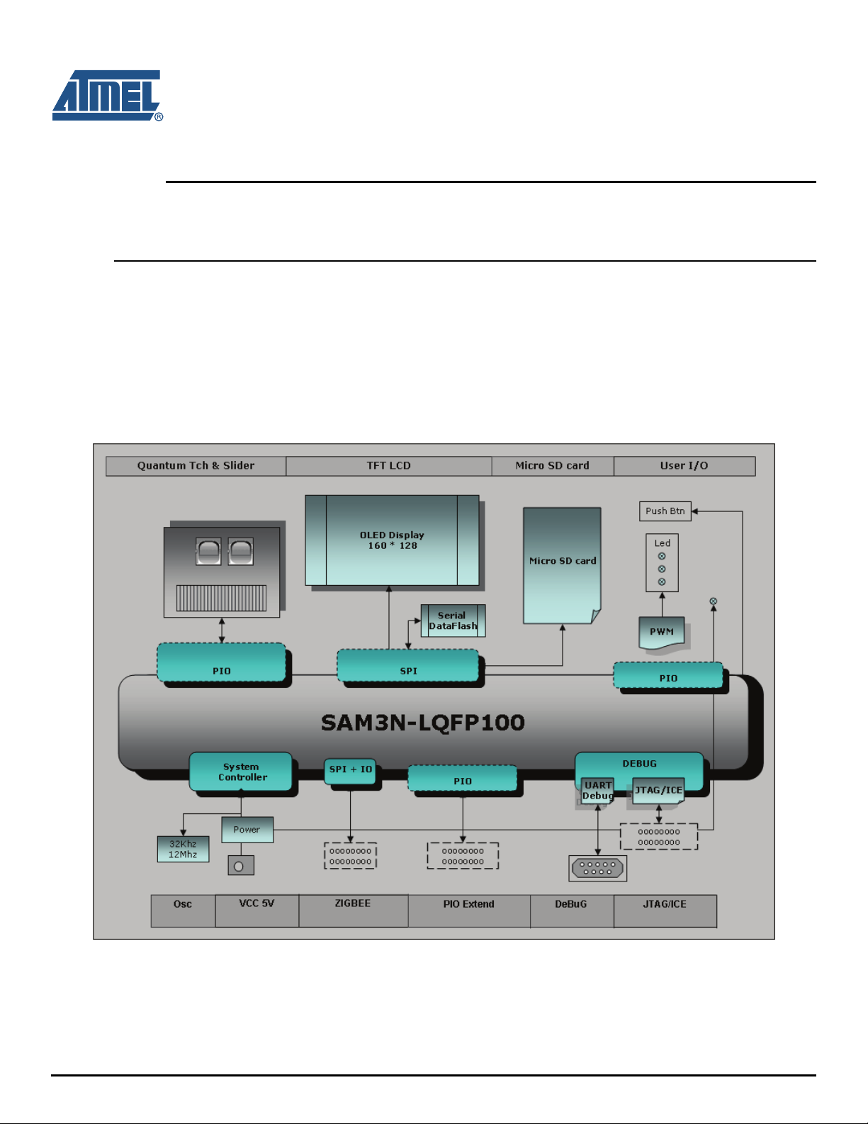
4.1 Board Overview
This section introduces the Atmel SAM3N Evaluation Kit design. It introduces system-level concepts,
such as power distribution, memory, and interface assignments.
The SAM3N-EK board is based on the integration of an ARM
Flash and a set of popular peripherals. It is designed to provide a high performance processor evaluation
solution with high flexibility for various kinds of applications.
Figure 4-1. SAM3N-EK Block Diagram
Section 4
Evaluation Kit Hardware
®
Cortex®-M3 processor with on-board
SAM3N-EK Development Board User Guide 4-1
11080C–ATARM–30-Mar-11
Page 9
Evaluation Kit Hardware
DATA FLASH
SPI MOSI
SPI MISO
SPI CLK
NPCS_DATAFLASH
PA12
PA13
PA14
PA22
+3V3
DGND
+3V3
+3V3
R32 0RR32 0R
R28 0RR28 0R
R29 10RR29 10R
MN7
AT25DF321
MN7
AT25DF321
NCS
1
SO
2
NWP
3
VCC
8
NHOLD
7
SCK
6
GND
4
SI
5
R27
47K
R27
47K
C35
100nF
C35
100nF
R31 0RR31 0R
4.2 Features List
Here is the list of the main board components and interfaces:
SAM3N4C QFP chip with optional socket footprint
12 MHz crystal
32.768 KHz crystal
32-Megabit Serial DataFlash
2.0 inch TFT color LCD display with backlight
UART port with level shifter IC
Micro SD interface
Reset buttons: NRST
User buttons: Left and Right
QTouch
JTAG port
On-board power regulation
Two user LEDs
Power LED
ZigBee
2x32 bit PIO connection interfaces (PIOA, PIOC) and 1x15 bit PIO connection interface (PIOB)
®
buttons: Left, Right, and Slider
®
connector
4.3 Function Blocks
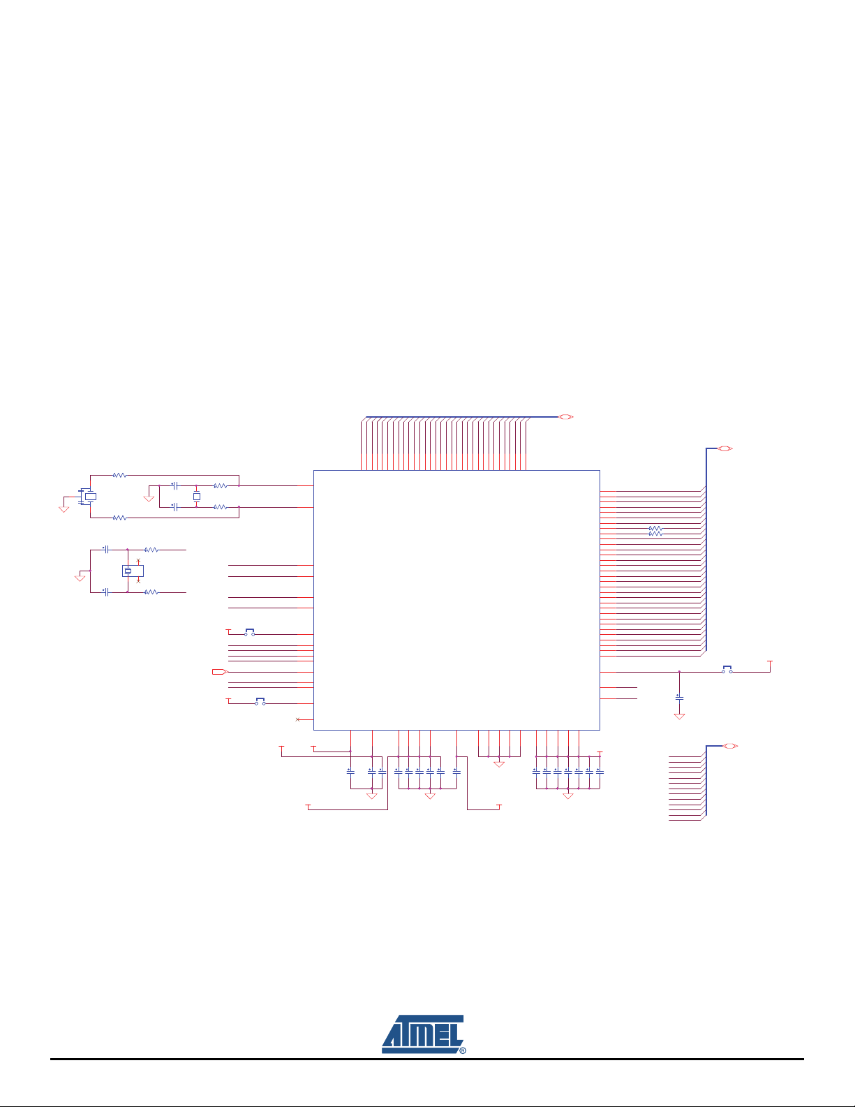
4.3.1 Processor
The SAM3N-EK is equipped with a SAM3N4C device in LQFP100 package.
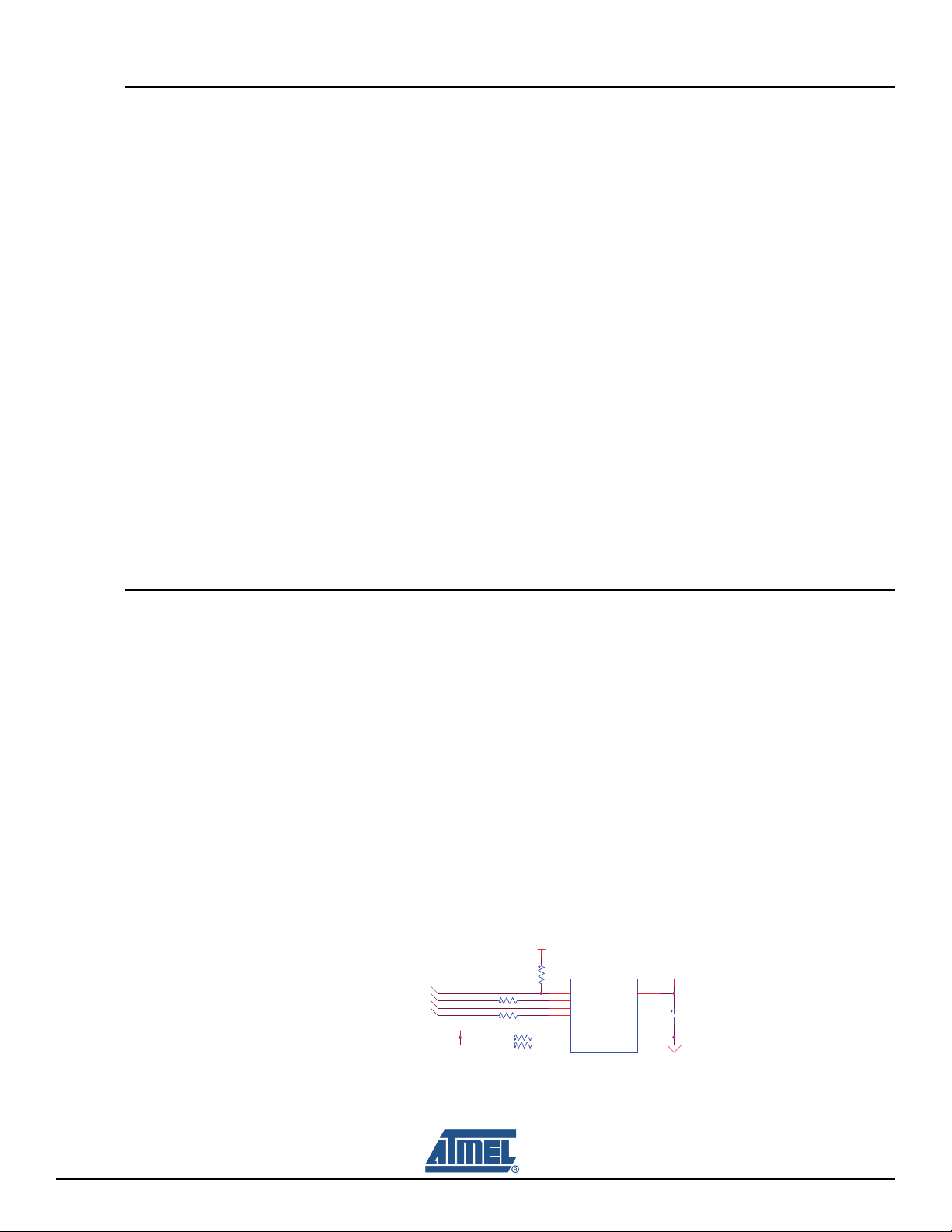
4.3.2 Memory
The SAM3N4 chip embeds:
256 Kbytes of embedded Flash
24 Kbytes of embedded SRAM with dual bank
16 Kbytes of ROM with embedded BootLoader routines (UART) and In-Application Programming
functions (IAP) routines.
The SAM3N-EK features an external DataFlash through SPI bus
Figure 4-2. DataFlash
NPCS3 chip select signal is used for DataFlash chip selection.
4-2 SAM3N-EK Development Board User Guide
11080C–ATARM–30-Mar-11
Page 10
DNP
XIN
PB2
PB3
PB10
PB11
PB4
PB6
PB7
PB5
NRST
PB1
PA0
PA1
PA2
PA3
PA4
PA5
PA6
PA9
PA10
PA11
PA12
PA13
PA14
PA15
PA16
PA17
PA18
PA19
PA20
PA21
PA22
PA23
PA24
PA25
PA26
PA27
PA28
PA29
PA30
PA31
P
C0
PC1
PC2
PC3PC4
PC5
PC6
PC7
P
C8
PC9
P
C
10
P
C11
PC12
PC13
P
C
14
P
C15
PC16
P
C17
P
C
18
PC19
PC20
PC
21
P
C22
PC
23
PC
24
PC25
P
C26PC
27
P
C28
P
C
29
PC30
PC
31
XOUT
XOUT32
PB0
JTAGSEL
XIN32
PB0
PB6
PB7
PB10
PB11
PB1
PB2
PB12
PB3
PB14
PB13
PB4
PB5
PB13
PB14
PB12
XIN32
XOUT32
PA7
PA8
ADVREF
DGND
DGND
VDDIO
DGND
DGND
DGND
VDDPLLVDDCORE
DGND
VDDINVDDOUT
DGND
DGND
+3V3
+3V3
+3V3
PA[0..31]
PC[0..31]
PB[0..14]
NRST
R1 DNPR1 DNP
C22 4.7uFC22 4.7uF
C13 100nFC13 100nF
R9 DNPR9 DNP
C7 100nFC7 100nF
C3
7pFC37pF
R2 0RR2 0R
C21
4.
7uFC214.7uF
C
10 100nFC10 100nF
C4
7pFC47pF
C20
100nF
C20
100nF
C
15 100nFC15 100nF
Y1Y1
1
2
3
C
19 100nFC19 100nF
JP3JP3
JP2JP2
C
12 100nFC12 100nF
Y3
32.768KHzY332.768KHz
1
2
3
4
C18 100nFC18 100nF
R7 DNPR7 DNP
C9
2.2uFC92.2uF
C17
100nF
C17
100nF
C5
100nFC5100nF
SAM3N - LQFP100
MN1
SAM3N4C-AU
SAM3N - LQFP100
MN1
SAM3N4C-AU
PA0_PWM0_TIOA0
74
PA1_PWM1_TIOB0
72
PA2_PWM2_SCK0_DATRG
67
PA3_TWD0_NPCS3
66
PA4_TWCK0_TCLK0
55
PA5_RXD0_NPCS3
53
PA6_TXD0_PCKO
52
PA7_RTS0_PWM3
49
PA8_CTS0_ADTRG
48
PA9_URXD0_NPCS1
46
PA10_UTXD0_NPCS2
44
PA11_NPCS0_PWM0
42
PA12_MISO_PWM1
41
PA13_MOSI_PWM2
33
PA14_SPCK_PWM3
31
PA15_TIOA1
30
PA16_TIOB1
28
PA17_PCK1_AD0
12
PA18_PCK2_AD1
14
PA19_AD2
18
PA20_AD3
24
PA21_RXD1_PCK1_AD8
15
PA22_TXD1_NPCS3_AD9
20
PA23_SCK1_PWM0
22
VDDCORE
85
JTAGSEL
77
GND
45
GND95GND
70
GND
26
VDDIO
27
VDDIO
69
VDDIO
91
PB8_XOUT
96
PB9_XIN
97
PB0_PWM0_AD4
3
NRST
60
VDDCORE
56
ADVREF
1
PA25_CTS1_PWM2
38
PA24_RTS1_PWM1
34
PB2_URXD1_NPCS2_AD6
7
PB3_UTXD1_PCK2_AD7
9
PB6_TMS_SWDIO
79
PB4_TWD1_PWM2_TDI
51
PB5_TWCK1_TDO_TACESWO
76
PB7_TCK_SWCLK
83
TEST
61
PB12_ERASE
87
PB14_NPCS1_PWM3
99
VDDOUT
11
PB1_PWM1_AD5
5
PA26_TIOA2
39
PA27_TIOB2
57
PA28_TCLK1
59
PA29_TCLK2
63
PA30_NPCS2
64
PA31_NPCS1_PCK2
81
VDDIN
10
PB10_DDM
88
PB11_DDP
89
PB13_PCK0_DAC0
93
VDDIO
98
VDDCORE
36
VDDCORE
16
VDDPLL
100
VDDIO
50
GND
2
PC0
25
PC1
47
PC2
43
PC3
40
PC4_NPCS1
37
PC5
35
PC6
32
PC7_NPCS2
29
PC8_PWM0
58
PC9_PWM1
62
PC10_PWM2
65
PC11_PWM3
68
PC12_AD12
23
PC13_AD10
21
PC14_PCK2
71
PC15_AD11
19
PC16_PCK0
73
PC17_PCK1
75
PC18_PWM0
78
PC19_PWM1
80
PC20_PWM2
82
PC21_PWM384PC22_PWM0
86
PC23_TIOA3
90
PC24_TIOB3
92
PC25_TCLK3
94
PC26_TIOA4
13
PC27_TIOB4
17
PC28_TCLK4
54
PC29_TIOA5_AD13
4
PC30_TIOB5_AD14
6
PC31_TCLK5_AD15
8
R50RR5
0R
C14 DNPC14 DNP
C8 100nFC8 100nF
Y2 12MHzY2 12MHz
C1 15pFC1 15pF
C16 100nFC16 100nF
R4 DNPR4 DNP
R3 0RR3 0R
R100RR10
0R
JP1
DNP
JP1
DNP
C2 15pFC2 15pF
C11 100nFC11 100nF
4.3.3 Clock Circuitry
The clock generator of a SAM3N microcontroller is made up of:
A Low Power 32,768 Hz Slow Clock Oscillator with bypass mode
A Low Power RC Oscillator
A 3 to 20 MHz Crystal Oscillator, which can be bypassed
A factory programmed fast internal RC Oscillator. 3 output frequencies can be selected: 4 (default
value), 8 or 12 MHz.
A 60 to 130 MHz programmable PLL (input from 3.5 to 20 MHz), capable to provide the clock MCK to
the processor and to the peripherals.
The SAM3N-EK board is equipped with one 12 MHz crystal, and one 32.768 Hz crystal. An optional
12 MHz Piezoelectric Ceramic Resonator can be mounted in place of the 12 MHz crystal (for low cost
clocking option evaluation).
Figure 4-3. SAM3N MCU
Evaluation Kit Hardware
4.3.4 Reset Circuitry
The on-board NRST button BP1 provides the SAM3N4C with external reset control.
Two User buttons BP2 and BP3, can be used to wake up the chip from low power modes.
The NRST pin is bidirectional. It is handled by the on-chip reset controller. It can be driven low to provide
a reset signal out to the external components. Conversely, it can be asserted low from the outside to
reset the microcontroller, its core and peripherals, with exception of the backup region (RTC, RTT and
SAM3N-EK Development Board User Guide 4-3
11080C–ATARM–30-Mar-11
Page 11

Evaluation Kit Hardware
+3V3+5V
DGND
C25
1uF
C25
1uF
C29
10uF 0805
C29
10uF 0805
J1
MP179P 2.1mm
J1
MP179P 2.1mm
1
2
3
+
C28
22uF
+
C28
22uF
MN4
LP38692MP-3.3
MN4
LP38692MP-3.3
VIN4VOUT
3
VEN1NC
2
GND
5
MN3
ZEN056V130A24LS
MN3
ZEN056V130A24LS
1
2
3
C27
100nF
C27
100nF
C26
10uF 0805
C26
10uF 0805
Supply Controller). The NRST pin integrates a permanent pull-up resistor of about 100 kOhm to VDDIO.
On the SAM3N-EK board, the NRST signal is connected to the JTAG port.
4.3.5 Power Supply and Management
The SAM3N-EK board is supplied with an external 5V DC block through the J1 socket. It is protected by
a PolyZen diode MN3. The PolyZen protects the board in the case of an incorrect power supply
connection.
The LDO regulator MN4 is used for the 3.3V main supply. It powers all the 3.3V components on the
board.
Figure 4-4. Power Block
4.3.6 UART
The SAM3N4/2/1 product series has different types of power supply pins:
VDDIN pin: Power for the internal voltage regulator, ADC, DAC, and analog comparator power
supplies. This voltage ranges from 1.8V to 3.6V.
VDDIO pin: Powers the Peripheral I/O lines, Backup part, 32 kHz crystal oscillator and oscillator pads.
This voltage ranges from 1.62V to 3.6V.
VDDOUT pin: Output of the internal voltage regulator.
VDDCORE pin: Powers the core, including the processor, the embedded memories and the
peripherals. This voltage ranges from 1.62V to 1.95V.
VDDPLL pin: Powers the PLL, the Fast RC and the 3 to 20 MHz oscillators. This voltage ranges from
1.62V to 1.95V.
The Universal Asynchronous Receiver Transmitter features a two-pin UART that can be used for communication and trace purposes. It offers an ideal channel for in-situ programming solutions. This UART
is associated with two PDC channels to reduce the processor time on packet handling.
The two-pin UART (TXD and RXD only) is buffered through an RS232 Transceiver MN8 and brought to
the DB9 male connector J4.
4-4 SAM3N-EK Development Board User Guide
11080C–ATARM–30-Mar-11
Page 12

Figure 4-5. UART
UART
PA10
PA9
+3V3
DGND
DGND
+3V3 +3V3
FGND
C39
100nF
C39
100nF
C40
100nF
C40
100nF
TP6
SMD
TP6
SMD
J4J4
5
4
3
2
1
9
8
7
6
10
11
R36
100K
R36
100K
R39 0RR39 0R
C38
100nF
C38
100nF
TP7
SMD
TP7
SMD
C41
100nF
C41
100nF
R40 0RR40 0R
R41 0RR41 0R
C42
100nF
C42
100nF
MN8
MAX3232CSE
MN8
MAX3232CSE
T1IN
11
T2IN
10
R1OUT
12
R2OUT
9
T1OUT
14
T2OUT
7
R1IN
13
R2IN
8
V+
2
C1+
1
C1-
3
C2+
4
C2-
5
V-
6
VCC
16
GND
15
R35
100K
R35
100K
4.3.7 Display Interface
The SAM3N-EK carries a TFT Transmissive LCD module with touch panel, TM020GDZ18. Its integrated
driver IC is ILI9225B. The LCD display area is 2.0 inches diagonally measured, with a native resolution
of 176x220 pixels.
The LCD module gets reset from GPIO PA29. The LCD chip select signal is connected to NPCS2. The
SAM3N communicates with the LCD through the SPI bus.
Evaluation Kit Hardware
Figure 4-6. LCD
4.3.8 Backlight Control
The LCD backlight is made of four integrated white chip-LEDs arranged in parallel. These are driven by
an AAT3193 charge pump, MN5. The AAT3193 is controlled by the SAM3N through a single PIO line
interface (PC13); the 0 Ohm resistor R17 is mounted in series on this line, which permits to use it for
other custom purposes. In that case, the pull-up resistor R64 maintains the charge pump permanently
enabled by default.
On the anode drive line, a 0 Ohm resistor R21 is implemented in series for an optional current limitation.
NPCS_LCD
SPI CLK
SPI MOSI
PA30
PA14
PA13
PA28
PA29
R19 0RR19 0R
DGND
+3V3
+
+
C31
C31
C30
C30
10uF
10uF
DGND
100nF
100nF
LED_A
LED_K1
LED_K2
LED_K3
R18
R18
47K
47K
R21 0RR21 0R
LCD
R60
R60
47K
47K
MN6
MN6
TM020GDZ18
TM020GDZ18
1
ID
2
NCS
3
SCL
4
SDA
5
RS
6
NREST
7
GND
8
IOVDD
9
VDD
10
LEDA
11
LEDK1
12
LEDK2
13
LEDK3
14
Y+
15
Y-
16
X+
17
X-
18
NC
11080C–ATARM–30-Mar-11
SAM3N-EK Development Board User Guide 4-5
Page 13

Evaluation Kit Hardware
PA1
DGND
+3V3
D5D5
B2
BN03K314S300R
B2
BN03K314S300R
R59
22R
R59
22R
MN9
SMD-050020F-03640
MN9
SMD-050020F-03640
+
1
-
2
Q2
IRLML2502
Q2
IRLML2502
1
32
R58
10K
R58
10K
Figure 4-7. Backlight
4.3.9 JTAG/ICE
A standard 20-pin JTAG/ICE connector is implemented on the SAM3N-EK for the connection of a compatible ARM JTAG emulator interface, such as the SAM-ICE from Segger.
Notes: 1. The NRST signal is connected to BP1 system button. The 0 ohm resistor R30 may be
+3V3
R16
+3V3
PC13
R170RR17
0R
B1
B1
BN03K314S300R
BN03K314S300R
DGND
R16
47K
47K
C33
C33
4.7uF
4.7uF
MN5
MN5
AAT3193IJQ-1-T1
AAT3193IJQ-1-T1
6
EN/SET
5
IN
RSET7OUT
R20
R20
19.1k,1%
19.1k,1%
8
GND
LCD BACKLIGHT
4
C+
C-
D1
D2
D3
C32
C32
1uF
1uF
3
2
LED_A
1
LED_K1
10
LED_K2
9
LED_K3
DGND
C34
C34
1uF
1uF
removed in order to isolate the JTAG port from this system reset signal.
2. The TDO pin is in input mode with the pull-up resistor disabled when the Cortex M3 is
not in debug mode. To avoid current consumption on VDDIO and/or VDDCORE due to
floating input, the internal pull-up resistor corresponding to this PIO line must be
enabled.
Figure 4-8. JTAG Connector
4.3.10 PWM Buzzer
A small, magnetic audio transducer connects through a MOSFET to PWM, allowing a range of options
for generating simple and complex tones.
Figure 4-9. PWM Buzzer
PB[0..14]
NRST
PB4
PB6
PB7
PB5
R22
R22
100K
100K
R23
R23
100K
100K
R24
R24
R25
R25
100K
100K
100K
100K
R30 0RR30 0R
ICE INT ERFACE
R26
R26
100K
100K
+3V3
J2J2
VTref1Vsupply
nTRST3GND1
TDI5GND2
TMS7GND3
TCK9GND4
RTCK11GND5
TDO13GND6
nSRST15GND7
DBGRQ17GND8
DBGACK19GND9
2
4
6
8
10
12
14
16
18
20
DGND
4.3.11 SD/MMC Card
The SAM3N has a high-speed 4-bit multimedia MMC interface, which is connected to a 4-bit SD/MMC
micro card slot featuring a card detection switch.
4-6 SAM3N-EK Development Board User Guide
11080C–ATARM–30-Mar-11
Page 14

Figure 4-10. SD Card
QTOUCH
PC9
PC11
PC8
PC10
PC0
PC1
PC3
PC2
PC4
PC5
R55 1KR55 1K
S1
DNPS1DNP
SL
SM
SR
SR
K1
DNPK1DNP
C50
22nF
C50
22nF
C46
22nF
C46
22nF
R57 1KR57 1K
R54 1KR54 1K
C47
22nF
C47
22nF
K2
DNPK2DNP
C48
22nF
C48
22nF
R53 1KR53 1K
C49
22nF
C49
22nF
R56 1KR56 1K
4.3.12 Touch Elements
QTouch keys consist of a series of sensors formed by the association of a copper area and the capacitive effect of human fingers approaching it.
Figure 4-11. QTouch Elements
NPCS_MicroSD
SPI MOSI
SPI CLK
SPI MISO
234
567
1
8
PA11
PA13
PA14
PA12
PA19
RA1
RA1
47KX4
47KX4
R37 0RR37 0R
R38 10RR38 10R
Micro SD CARD in SPI Mode
Evaluation Kit Hardware
+3V3
+
+
C37
C37
C36
C36
100nF
100nF
10uF
10uF
R34
R34
R33
R33
10K
10K
10K
10K
DGND
DGND
1
2
3
4
5
6
7
8
10
9
J3
TF01AJ3TF01A
RSV(DAT2)
CS(DAT3)
DI(CMD)
VCC
CLK
VSS
DO(DAT0)
RSV(DAT1)
GND
CD
11
Sh1
12
Sh2
13
Sh3
DGND
Keys
The SAM3N-EK implements two individual capacitive touch keys (RIGHT, LEFT) using two pairs of
PIOs.
Slider
A group of channels forms a Slider. A Slider is composed of three channels for a QTouch acquisition
method using three pairs of PIOs. Such a sensor is used to detect a linear finger displacement on a sensitive area. A typical slider implementation is volume control.
4.3.13 User Buttons
There are two mechanical user buttons on the SAM3N-EK, which are connected to PIO lines and
defined to be "left" and "right" buttons by default.
In addition, a mechanical button controls the system reset, signal NRST.
SAM3N-EK Development Board User Guide 4-7
11080C–ATARM–30-Mar-11
Page 15

Evaluation Kit Hardware
BUT TONS
PA15
PA16
DGND
NRST
BP1BP1
1
42
3
BP3BP3
1
42
3
BP2BP2
1
42
3
Figure 4-12. User Buttons
4.3.14 LEDs
There are four LEDs on the SAM3N-EK board:
A blue LED (D1), a green LED (D2), and an amber LED (D3) which are user-defined and controlled by
the GPIO.
A red LED (D4), which is a power LED indicating that the 3.3V power rail is active. It is also controlled
by the GPIO and can be treated as a user LED as well. The only difference with the three others is that
it is controlled through a MOS transistor. By default, the PIO line is disabled; a pull-up resistor controls
the MOS to light the LED when the power is ON.
Figure 4-13. LEDs
PA23
R42
R42
470R
470R
+3V3
D1 Blue-ledD1 Blue-led
4.3.15 ZigBee
PB14
PA25
PA0
IRLML2502
IRLML2502
DGND
470R
R44
R44
470R
470R
1
Q1
Q1
R46
R46
470R
470R
32
D2 Green-ledD2 Green-led
D3 Amber-le dD3 Amber-le d
R45 100KR45 100K
D4 Red-ledD4 Red-led
R43
R43
470R
SAM3N-EK has a 10-pin male connector for the RZ600 ZigBEE module.
Note: 0 Ohm resistors have been implemented in series with the PIO lines that are used else-
where in the design, thereby enabling their individual disconnection, should a conflict occur
in your application.
Figure 4-14. ZigBee
J7J7
ZB_RSTN
IRQ1_ZBEE
CS
MISO
R47 0RR47 0R
PC23
R48 0RR48 0R
PA31
R51 10RR51 10R
PA12 PA14
1 2
3 4
5 6
7 8
9 10
R49 0RR49 0R
R50 0RR50 0R
R52 0RR52 0R
C43
C43
18pF
18pF
C44
C44
2.2nF
2.2nF
PC24
PC26PC25
PA13
DGND
C45
C45
2.2uF
2.2uF
IRQ0_ZBEE
SLP_TR
MOSI
SPCK
+3V3
4.3.16 PIO Expansion
The SAM3N product features three PIO controllers, PIOA, PIOB and PIOC, which are multiplexed with
the I/O lines of the embedded peripherals. Each PIO Controller controls up to 32 lines (15 for PIOB).
4-8 SAM3N-EK Development Board User Guide
11080C–ATARM–30-Mar-11
Expansion ports J5, J6 provide PIO lines access for customer defined usage.
Page 16

Evaluation Kit Hardware
PA0
PA1
PA2
PA3
PA4
PA5
PA6
PA7
PA8
PA9
PA10
PA11
PA12
PA13
PA14
PA15
PA19
PA17
PA21
PA16
PA20
PA18
PA27
PA29
PA26
PA30
PA31
PA28
PA25
PA24
PA23
PA22 PC12
PC13
PC14
PC15
PC16
PC17
PC18
PC19
PC20
PC21
PB10
PB11
PB12
PC6
PB14
PB13
PC24
PC23
PC22
PC25
PC27
PC26
PC29
PC30
PC31
PC28
PB2
PB1
PB4
PB5
PB6
PB3
PB0 PB7
+3V3 +3V3 +3V3+3V3
DGND DGND DGND
DGND
+3V3 +5V +5V+3V3
PA[0..31]
PB[0..14]
PC[0..31]
JP9JP9
1
2
3
JP8JP8
1
2
3
J6J6
1 2
3 4
5 6
7 8
9 10
11 12
13 14
15 16
17 18
19 20
21 22
23 24
25 26
27 28
29 30
31 32
33 34
35 36
37 38
39 40
J5J5
1 2
3 4
5 6
7 8
9 10
11 12
13 14
15 16
17 18
19 20
21 22
23 24
25 26
27 28
29 30
31 32
33 34
35 36
37 38
39 40
Note: All PIO lines are available on these expansion connectors, except those that are used for
the QTouch elements.
Figure 4-15. PIO Expansion
4.4 Configuration
This section describes the PIO usage, the jumpers, the test points and the solder drops of a SAM3N-EK
board.
4.4.1 PIO Usage
Table 4-1. PIO Port A Assignment
I/O Line Peripheral A Peripheral B Peripheral C Extra Function EK Usage Device
PA0 PWM0 TIOA0 WKUP00 POWER LED Led Red
PA1 PWM1 TIOB0 WKUP01 CMD_SOUND BUZZER
PA 2 P W M2 S CK 0 DAT R G W KU P0 2
PA 3 T WD 0 N P CS 3 WK U P 03
PA 4 T WC K 0 T C LK 0
PA5 RXD0 NPCS3 WKUP04
PA 6 T XD 0 P C K0
PA7 RTS0 PWM3 XIN32 32K Crystal
PA8 CTS0 ADTRG WKUP05 XOUT32 32K Crystal
11080C–ATARM–30-Mar-11
PA9 URXD0 NPCS1 WKUP06 RX_UART0 UART
PA10 UTXD0 NPCS2 TX_UART0 UART
PA11 NPCS0 PWM0 WKUP07 SPI_NPCS0# MicroSD
SAM3N-EK Development Board User Guide 4-9
Page 17

Evaluation Kit Hardware
Table 4-1. PIO Port A Assignment (Continued)
I/O Line Peripheral A Peripheral B Peripheral C Extra Function EK Usage Device
LCD
PA12 MISO PWM1 SPI_MISO
PA13 MOSI PWM2 SPI_MOSI
PA14 SPCK PWM3 WKUP08 SPI_SPCK
PA15 TIOA1 WKUP14 PB_LEFT# Push Button Left
PA16 TIOB1 WKUP15 PB_RIGHT# Push Button Right
PA17 PCK1 AD0
PA18 PCK2 AD1
MicroSD
DataFlash
Zigbee
LCD
MicroSD
DataFlash
Zigbee
LCD
MicroSD
DataFlash
Zigbee
PA19 AD2/ WKUP09 MicroSD_CD MicroSD
PA20 AD3/ WKUP10
PA21 RXD1 PCK1 AD8
PA22 TXD1 NPCS3 AD9 SPI_NPCS3# DataFlash
PA23 SCK1 PWM0 USR_LED1# Led Blue
PA24 RTS1 PWM1
PA25 CTS1 PWM2 USR_LED3# Led Amber
PA 26 T I OA 2
PA 27 T I OB 2
PA28 TCLK1 RS_LCD LCD
PA29 TCLK2 RST_LCD LCD
PA30 NPCS2 WKUP11 SPI_NPCS2# LCD
PA31 NPCS1 PCK2 SPI_NPCS1# ZigBee
Table 4-2. PIO Port B Assignment
I/O Line Peripheral A Peripheral B Peripheral C Extra Function EK Usage Device
PB0 PWM0 AD4
PB1 PWM1 AD5
PB2 URXD1 NPCS2 AD6/ WKUP12
PB3 UTXD1 PCK2 AD7
PB4 TWD1 PWM2 TDI JTAG
PB5 TWCK1 WKUP13
4-10 SAM3N-EK Development Board User Guide
11080C–ATARM–30-Mar-11
TDO/
TRACESWO
JTAG
Page 18

Evaluation Kit Hardware
Table 4-2. PIO Port B Assignment (Continued)
I/O Line Peripheral A Peripheral B Peripheral C Extra Function EK Usage Device
PB6 TMS/SWDIO JTAG
PB7 TCK/SWCLK JTAG
PB8 XOUT_12M 12M Crystal
PB9 XIN_12M 12M Crystal
PB10
PB11
PB12 ERASE JUMPER
PB13 PCK0 DAC0
PB14 NPCS1 PWM3 USR_LED2# Led Green
Table 4-3. PIO Port C Assignment
I/O Line Peripheral A Peripheral B Peripheral C Extra Function EK Usage Device
PC0 QT_SL_SNS QTOUCH_SLIDER
PC1 QT_SL_SNSK QTOUCH_SLIDER
PC2 QT_SM_SNS QTOUCH_SLIDER
PC3 QT_SM_SNSK QTOUCH_SLIDER
PC4 NPCS1 QT_SR_SNS QTOUCH_SLIDER
PC5 QT_SR_SNSK QTOUCH_SLIDER
PC6
PC7 NPCS2
PC8 PWM0 QT1_ SNS QTOUCH_KEY_Left
PC9 PWM1 QT1_ SNSK QTOUCH_KEY_Left
PC10 PWM2 QT2_ SNS QTOUCH_KEY_Right
PC11 PWM3 QT2_ SNSK QTOUCH_KEY_Right
PC12 AD12
PC13 AD10 EN_LCD LCD
PC14 PCK2
PC15 AD11
PC16 PCK0
PC17 PCK1
PC18 PWM0
PC19 PWM1
PC20 PWM2
PC21 PWM3
PC22 PWM0 AD16
PC23 TIOA3 ZB_RSTN ZigBee
SAM3N-EK Development Board User Guide 4-11
11080C–ATARM–30-Mar-11
Page 19

Evaluation Kit Hardware
Table 4-3. PIO Port C Assignment (Continued)
I/O Line Peripheral A Peripheral B Peripheral C Extra Function EK Usage Device
PC24 TIOB3 ZB_IRQ0 ZigBee
PC25 TCLK3 ZB_IRQ1 ZigBee
PC26 TIOA4 ZB_SLPTR ZigBee
PC27 TIOB4
PC28 TCLK4
PC29 TIOA5 AD13
PC30 TIOB5 AD14
PC31 TCLK5 AD15
4.4.2 Jumpers
The SAM3N-EK board jumpers are used for many purposes such as internal Flash Memory reinitialization, power current measurement and other configurations.
Table 4-4. Jumpers
Default
Designation Label
JP1 JTAGSEL OPEN
Setting Feature
Close it to reinitialize the Flash content and some
of its NVM bits.
This jumper must be closed for more than 220 ms
at power-up to perform the reinitialization.
4.4.3 Test Points
Some test points have been placed on the SAM3N-EK board for the verification of important signals.
Table 4-5. Test Points
Designation Part Description
TP1 Ring Hook +5V
TP2 Ring Hook +3V3
TP3 Ring Hook GND
TP4 Ring Hook GND
JP2 ADVREF CLOSE
JP3 PB12 OPEN
JP4 VDDIO CLOSE Access for current measurement on VDDIO
JP5 VDDIN CLOSE Access for current measurement on VDDIN
JP6 VDDPLL CLOSE Access for current measurement on VDDPLL
JP7 VDDCORE CLOSE Access for current measurement on VDDCORE
JP8 +3V3 1-2
JP9 +3V3 1-2
Analog reference voltage selection, access for
external reference voltage
ERASE, Close to reinitialize the Flash contents and
some of its NVM bits
DC voltage selection between 3.3V and 5V on PIO
expansion ports, default for 3.3V
DC voltage selection between 3.3V and 5V on PIO
expansion ports, default for 3.3V
4-12 SAM3N-EK Development Board User Guide
11080C–ATARM–30-Mar-11
Page 20

Table 4-5. Test Points (Continued)
Designation Part Description
TP5 Ring Hook GND
TP6 Pad UTXD0
TP7 Pad URXD0
4.4.4 Assigned PIO Lines, Disconnection Possibility
As pointed out in previous interface descriptions, 0-Ohm resistors have been inserted on the PIO lines
receiver path of the SAM3N-EK. Some PIO lines are connected to an external driver on the board. The
0-Ohm resistors allow disconnecting each of these for custom usage (through PIO expansion connectors, for example). This feature gives the user an added level of versatility for prototyping a system of his
own. See the table below.
Table 4-6. Disconnection Possibility
Designation Default Assignment PIO
R2 XIN PB9
R3 XOUT PB8
R9, R5 XIN32 PA7
R4, R10 XOUT32 PA8
R17 EN_LCD PC13
Evaluation Kit Hardware
R39 URXD0 PA9
R40 UTXD0 PA10
R47 ZB_RSTN PC23
R48 IRQ1_ZBEE PC25
R49 IRQ0_ZBEE PC24
R50 SLP_TR PC26
SAM3N-EK Development Board User Guide 4-13
11080C–ATARM–30-Mar-11
Page 21

5.1 Overview
Section 5
QT600
The QT600 is an integrated board added in the kit that allows you to develop and debug any application
using the Atmel QTouch Library
to start developing touch solutions on Atmel ATx Microcontrollers.
QT600 is fully supported by QTouch Library and AVR Studio
QTouch Suite
Figure 5-1. SAM3N-EK and QT600 Connection
™
.
™
. QT600 has been designed to give developers a quick and easy way
®
, and together these tools form the Atmel
SAM3N-EK Development Board User Guide 5-1
11080C–ATARM–30-Mar-11
Page 22

QT600
SAM3N-EK
MCU Board + Touch
QT600
Interface Board
Interface between
To uch MCU and PC
PC Front-End
USB
QTouch Studio
SPI or PIO
5.2 System Description
The development system is based on two boards connected together:
QT600 Interface Board
SAM3N-EK Board with Touch Sensor
Figure 5-2. QT600 System Block Diagram
The QT600 Interface board is used to stream live touch data from the SAM3N-EK board.
QTouch Studio
5.3 Features
Live streaming of touch data to QTouch Studio
USB Interface to PC for programming and streamed QTouch Debug data
Powered from USB bus
™
is used as the PC front-end, for visualization of the touch data.
5-2 SAM3N-EK Development Board User Guide
11080C–ATARM–30-Mar-11
Page 23
5.4 Getting Started
To use the QT600 interface, it is necessary to have QTouch Studio™ 3.4.0 or later installed. Download
the latest version from www.atmel.com.
Download and install the “Atmel_QTouch_Libraries_4.3_SAM3N_Patch.exe” and follow the installation
steps as detailed below:
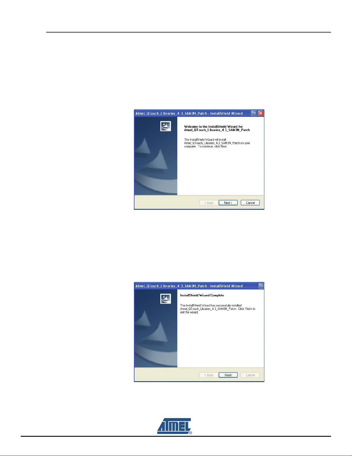
1. Start the installation process
Figure 5-3. Installation Step 1
QT600
2. Accept the terms of the licence agreement
3. Choose the destination location of the folder
4. Update the QT600 firmware
5. Install the program
6. When the installation is complete, click the “Finish” button
Figure 5-4. Installation Step 6
SAM3N-EK Development Board User Guide 5-3
11080C–ATARM–30-Mar-11
Page 24

QT600
The SAM3N-EK boards must be programmed with the QTouch application code. For ARM products, the
examples can be retrieved from the QTouch Library (installation process described on page 5-3).
The example projects must be compiled for the application to work. Refer to the main.c file in each project for details.
For the SPI interface, the project files are located in:
C:\ProgramFiles\Atmel\Atmel_QTouch_Libraries_4.3\Generic_QTouch_Libraries\AT91SAM\SAM3\
QTouch\example_projects\sam3n4_iar_qt_example_spi
For the PIO interface, the project files are located in:
C:\ProgramFiles\Atmel\Atmel_QTouch_Libraries_4.3\Generic_QTouch_Libraries\AT91SAM\SAM3\
QTouch\example_projects\sam3n4_iar_qt_example
The Touch Data LED on the QT600 indicates the mode:
Touch Data LED green: Touch Debug Mode (default mode after power-up).
Touch Data LED off: Programmer Mode
Make sure that the Touch Data LED is off before attempting to connect to the QT600 from the QTouch
Studio programming dialog. Use AVR Studio 4.18 or later.
1. Connect the 10 wire flat-cable between the Touch Data header on the QT600 and the selected
SAM3N-EK board (see Figure 5-9 on page 5-7)
2. Make sure that VTG header is open on the QT600 (see “Target Voltage VTG” on page 5-8)
3. Start AVR QTouch Studio
4. Plug in the USB cable to the QT600. AVR QTouch Studio should now automatically connect to the
SAM3N-EK
5. Press the Start Debug button
You should now be able to view the touch data signals and the state of each sensor.
5-4 SAM3N-EK Development Board User Guide
11080C–ATARM–30-Mar-11
Page 25

Figure 5-5. QTouch Studio GUI
QT600
5.5 Hardware Description
5.5.1 QT600 Interface Board
Figure 5-6. QT600 Interface Board
The QT600 Interface Board is the communication interface between the touch system (presently
SAM3N-EK) and the AVR QTouch Studio. It receives touch signal data from the MCU running the
QTouch Library, and forwards this data to the AVR QTouch Studio for visual presentation.
The QT600 can also be used as a programmer for programming the on-chip flash memory of the microcontrollers on the SAM3N-EK board.
SAM3N-EK Development Board User Guide 5-5
11080C–ATARM–30-Mar-11
Page 26

QT600
Figure 5-7. QT600 Interface Board Block Diagram
5-6 SAM3N-EK Development Board User Guide
11080C–ATARM–30-Mar-11
Page 27

5.5.2 TOUCH DATA Connectors
SDA SCL
RxD TxD
SS MOSI
MISO SCK
GND VTG
1 2
PA 31PA13
PA 12 PA 14
GND
1 2
In PIO modeIn SPI mode
Figure 5-8. TOUCH DATA Connector Pinout
The TOUCH DATA connector located on the QT600 interface board is used for streaming touch data to
the PC using the SPI (or PIO) interface. The corresponding connector is located on the Touch SAM3NEK board. A straight 10-wire cable can be connected between these two connectors.
Table 5-1. TOUCH DATA Connector Pinout
Pin Interface Name
QT600
Direction, QT600
interface board Direction SAM3N-EK Remarks
1
TWI
2 SCL Bi-directional Bi-directional
3
UART
4 TxD Input Output
5
6 MOSI Input Output
SPI
7 MISO Output Input
8 SCK Input Output
9ALL GND
10 ALL VTG Keep Jumper Open
SDA Bi-directional Bi-directional
Not used
RxD Output Input
Not used
SS Input Output
Figure 5-9. TOUCH DATA Connector
To uch Data
Connectors
To uch Data
J7
SAM3N-EK Development Board User Guide 5-7
11080C–ATARM–30-Mar-11
Page 28

QT600
5.5.3 Target Voltage VTG
The VTG is supplied by the MCU board through the 10-wire cable (connected to the TOUCH DATA
Connector).
Figure 5-10. VTG
Keep
open
5.5.4 VTG LED
A green LED labeled VTG on the QT600 board is lit when a voltage of 0.9V or higher is available on the
VTG net.
5.5.5 TOUCH DATA LED
The status of the LED indicates the operating mode of the QT600.
5.5.5.1 Touch Streaming Mode
When the QT600 is in Touch streaming mode (for use with AVR QTouch Studio), the TOUCH DATA
LED is green. When touch data is received from the SAM3N-EK, the LED starts to flash.
5.5.5.2 Programming Mode
When the QT600 is in programming mode (for use with AVR Qtouch Studio), the TOUCH DATA LED is
not lit.
5-8 SAM3N-EK Development Board User Guide
11080C–ATARM–30-Mar-11
Page 29

5.5.6 STATUS LED
Green: Ready state
Orange: Busy programming
Orange/red flashing: Upgrade mode
Orange/green flashing: Upgrade mode, upgrade in progress
During programming, the LED is orange. When the Atmel target device has been successfully programmed, the LED turns green.
5.5.7 Touch ATx Firmware
The firmware for the Touch ATx is based on the QTouch Library. The QTouch Library handles the touch
acquisition. The touch measurement values are made available for the application firmware trough an
API, which is described in detail in the QTouch Library User Guide.
The touch measurement values available through the Touch Library API are sent to the QT600 with an
SPI (or PIO) interface, using a custom protocol. AVR QTouch Studio will read these data packets from
the QT600.
See the QT600 Protocol Document for details about the communication protocol.
QT600
5.6 Touch Debug
Before a touch debug session can be started, the target microcontroller on the SAM3N-EK board must
be programmed. The example projects can be retrieved from the QTouch Library (installation steps are
detailed in Section 5.4).
Example projects for both GCC and IAR compilers are available.
1. Connect a 10-wire cable between the Touch Data Connector on the SAM3N-EK board and the Touch
Data connector on the QT600 Interface board (see Figure 5-9 on page 5-7)
2. Start AVR QTouch Studio
3. Connect the USB cable to the QT600 interface board
4. Press the Start Debug Button in AVR QTouch Studio
AVR QTouch Studio automatically connects to the QT600 when the USB plug is inserted. The Touch
Data streaming starts when the "Start Debug" button is pressed.
5.7 Using QT600 and AVR QTouch Studio for Custom Applications
The QT600 Interface Board and QTouch Studio can be used to read touch data from any application
based on the QTouch Library. The only requirement is that there are two I/O pins available and that there
is enough free space in flash for the debug protocol and serial interface driver.
The QT600 interface uses an SPI protocol at a frequency of 200 kHz.
Complete firmware driver files are available in the QT600 example projects, which can be downloaded
from www.atmel.com/QT600. See the readme.txt file in the QT600 Example Projects folder for instructions on how to add the QT600 protocol files to your firmware project.
SAM3N-EK Development Board User Guide 5-9
11080C–ATARM–30-Mar-11
Page 30

QT600
5.8 Troubleshooting and Support
5.8.1 Technical Support
For technical support, contact at91@atmel.com. When requesting technical support for the QT600, you
should provide the following information:
PC processor type and speed
PC operating system and version
Atmel target device used (complete part number)
Tar g e t v o l t ag e
Jumper settings
A detailed description of the problem
5.8.2 Force Firmware Upgrade
Before starting the procedure, make sure that the latest AVR Studio release (4.0 or later) has been
installed on your PC.
1. If connected to the PC with a USB cable, unplug the QT600.
2. Press and hold the button on QT600 when connecting the USB cable: the status LED flashes red
and orange, indicating the upgrade mode.
3. In AVR Studio, go to the Tools menu and select QT600 Upgrade.
4. The Atmel QT600 Upgrade program starts. If a connection has been established, the Status shows
"QT600 present".
5. Press the Start Upgrade button: the upgrade program upgrades QT600's firmware.
6. When complete, a message box indicates if the upgrade was successful or not. Disconnect and then
reconnect the USB cable.
7. If the upgrade was successful, the status LED turns green. Try to connect to the starter kit with
QTouch Studio.
The QT600 USB Bridge firmware must be updated using the batch file available in
“C:\...\QT600_USB_Bridge_Update” folder before using the Example projects.
Figure 5-11. USB Connector
5-10 SAM3N-EK Development Board User Guide
11080C–ATARM–30-Mar-11
Page 31

6.1 Schematics
This section contains the following schematics:
Block Diagram
Reference Guide
Microcontroller, Power
DataFlash, Micro SD, LCD, BL Driver, JTAG, RS232
IO Expansion, Buzzer, ZigBEE, LEDs, Buttons, QTouch
Section 6
Schematics
SAM3N-EK Development Board User Guide 6-1
11080C–ATARM–30-Mar-11
Page 32

5
4
3
2
1
D D
SAM3N-EK RevA Block Diagram
ATMEL Cortex M3 Processor SAM3N (LQFP100)
C C
PBs, LEDs
BUZZER
RS232
B B
SPI LCD
DATA Flash
QTouch
JTAG
ZIGBEE
User Interface (PIO Port A,B,C)
A A
05-MAY-10NLB
05-MAY-10NLB
INIT EDIT
INIT EDIT
INIT EDIT
A
A
A
REV
REV
REV
SCALE
SCALE
SAM3N-EK
SAM3N-EK
SAM3N-EK
Block Diagram
Block Diagram
Block Diagram
This agreement is our property. Reproduction and publication without our written authorization shall expose offender to legal proceedings.
This agreement is our property. Reproduction and publication without our written authorization shall expose offender to legal proceedings.
5
4
3
This agreement is our property. Reproduction and publication without our written authorization shall expose offender to legal proceedings.
2
SCALE
1/1
1/1
1/1
DES.
DES.
DES.
05-MAY-10NLB
05-MAR-10
05-MAR-10
05-MAR-10
DATE
DATE
DATE
1
XX-XXX-XXNL XXX
XX-XXX-XXNL XXX
XX-XXX-XXNL XXX
DATEMODIF.
VER.
DATEMODIF.
VER.
DATEMODIF.
VER.
REV. SHEET
REV. SHEET
REV. SHEET
1
1
1
B
B
B
5
5
5
Page 33

5
4
3
2
1
D D
REVISION HISTORY
REV DATA
A
2010.03.04 ORIGINAL RELEASED
NOTE
SCHEMATICS CONVENTIONS
(1) Resistance Unit: "K" is "Kohm", "R" is "Ohm?
(2) "DNP" means the component is not populated
by default
JUMPER and SOLDERDROP
PAGE REFERENCE FUNCTION
JP1
JP2
DEFAULT
DNP Close to select JTAG boundary scan
1-2
Analog reference voltage selection between 3.3V and 3V,
default 3.3V
JP3
OPEN
ERASE, Close to reinitialize the Flash contents and
some of its NVM bits
TABLE OF CONTENTS
3
TEST POINT
PAGE
C C
1
2
3
4
5
DESCRIPTION
Block Diagram
Reference guide
Microcontroller, Power
Data Flash, Micro SD, LCD, BL Driver,
JTAG, RS232
IO Expansion, Buzzer, ZigBEE, LEDs,
Buttons, QTouch
PAGE REFERENCE FUNCTION
3
TP1
TP2
TP3, TP4, TP5
TP6
+5V
+3V3
GND
UTXD04
TP7 URXD0
5
PIO MUXING
B B
PIOA USAGE
PA0
POWER LED
PA1
CMD_SOUND
PA2
PA3
PA4
PA5
PA6
PA7
XIN32
PA8
XOUT32 / ADTRG
PA9
RX_UART0
PA10
TX_UART0
PA11
PA12
PA13
PA14
PA15
SPI_MISO
SPI_MOSI
SPI_SPCK
PB_USER1
5
A A
PIOA USAGE
PA16
PB_USER2
PA17
PA18
PA19
MicroSD_CD
PA20
PA21
PA22
NPCS_DATAFLASH
PA23
LED_BLUE
PA24
PA25
LED_AMBER
PA26
PA27
PA28
RS_LCD
PA29
RST_LCD EN_LCD
NPCS_LCD
PA30
NPCS_ZigBee
PA31
PIOB USAGE
PB0
PB1
PB2
PB3
PB4
JTAG
PB5
JTAG
PB6
JTAG
PB7
JTAG
PB8
XOUT_12M
PB9
XIN_12M
PB10
PB11
ERASE
PB12
PB13
LED_GREEN
PB14
4
PIOC USAGE
PC0
QT_SL_SNS
PC1
QT_SL_SNSK
PC2
QT_SM_SNS
PC3
QT_SM_SNSK
PC4
QT_SR_SNS
PC5
QT_SR_SNSK
PC6
PC7
PC8
QT1_SNS
PC9
QT1_SNSK
PC10
QT2_SNS
PC11
QT2_SNSK
PC12
PC13
PC14
PC15
PIOC USAGE
PC16
PC17
PC18
PC19
PC20
PC21
PC22
PC23
ZB_RSTN
PC24
ZB_IRQ0
PC25
ZB_IRQ1
PC26
ZB_SLPTR
PC27
PC28
PC29
PC30
PC31
3
JP4
JP5
JP6
JP7
JP8
JP9
CLOSE
CLOSE
CLOSE
1-2
Access for current measurement on VDDIOCLOSE
Access for current measurement on VDDIN
Access for current measurement on VDDPLL
Access for current measurement on VDDCORE
DC voltage selection between 3.3V and 5V on PIO
expansion ports, default for 3.3V
DEFAULT NO POPULATE PARTS
PAGE REFERENCE FUNCTION
JP1 Option access for JTAGSEL
3
R6, R8
R4, R9
S1, K1, K2 QTouch PADs, not real part
5
2
External clock resource inputY1, R1, R7
Isolation between 12MHz clock source and GPIO line
Isolation between 32KHz clock source and GPIO line
SAM3N-EK
SAM3N-EK
SAM3N-EK
Describe
Describe
Describe
This agreement is our property. Reproduction and publication without our written authorization shall expose offender to legal proceedings.
This agreement is our property. Reproduction and publication without our written authorization shall expose offender to legal proceedings.
This agreement is our property. Reproduction and publication without our written authorization shall expose offender to legal proceedings.
05-MAY-10NLB
05-MAY-10NLB
05-MAY-10NLB
05-MAR-10
05-MAR-10
INIT EDIT
INIT EDIT
INIT EDIT
A
A
A
REV DATEMODIF. DES. DATE VER.
REV DATEMODIF. DES. DATE VER.
REV DATEMODIF. DES. DATE VER.
SCALE
SCALE
SCALE
1/1
1/1
1/1
05-MAR-10
1
XX-XXX-XXNL XXX
XX-XXX-XXNL XXX
XX-XXX-XXNL XXX
REV. SHEET
REV. SHEET
REV. SHEET
2
2
2
B
B
B
5
5
5
Page 34

5
D D
R1 DNPR1 DNP
12
3
Y1Y1
DNP
DGND
R7 DNPR7 DNP
C3
7pFC37pF
1
DGND
C C
+3V3
B B
VDDOUT
A A
4
C4
7pFC47pF
JP4JP4
JP5JP5
10uF
10uF
JP6JP6
JP7JP7
VDDIO
VDDIN
C23
C23
DGND
VDDCORE
23
+
+
VDDPLL
DGND
R50RR5
0R
Y3
32.768KHzY332.768KHz
R100RR10
0R
C1 15pFC1 15pF
C2 15pFC2 15pF
XIN32
XOUT32
R2 0RR2 0R
Y2 12MHzY2 12MHz
R3 0RR3 0R
NRST{4,5}
+3V3
+3V3
JP1
JP1
DNP
DNP
4
JP3JP3
XIN
XOUT
PB2
PB3
PB10
PB11
JTAGSEL
PB4
PB6
PB7
PB5
NRST
PB0
PB1
PB12
J1
J1
MP179P 2.1mm
MP179P 2.1mm
3
MN1
MN1
SAM3N4C-AU
SAM3N4C-AU
97
PB9_XIN
96
PB8_XOUT
7
PB2_URXD1_NPCS2_AD6
9
PB3_UTXD1_PCK2_AD7
88
PB10_DDM
89
PB11_DDP
77
JTAGSEL
51
PB4_TWD1_PWM2_TDI
79
PB6_TMS_SWDIO
83
PB7_TCK_SWCLK
76
PB5_TWCK1_TDO_TACESWO
60
NRST
3
PB0_PWM0_AD4
5
PB1_PWM1_AD5
87
PB12_ERASE
61
TEST
VDDINVDDOUT
MN3
MN3
ZEN056V130A24LS
ZEN056V130A24LS
1
1
2
3
PC0
PC1
PC2
PC3
PC4
PC5
PC6
PC7
PC8
PC9
PC10
PC11
PC12
PC13
PC14
PC15
PC16
PC17
PC18
PC19
PC20
PC21
PC22
PC23
PC24
PC25
PC26
PC27
PC28
PC29
PC30
PC31
40
37
32
29
62
65
68
21
71
19
75
78
80
82
84
86
90
92
94
13
17
54
4
6
8
PC025PC147PC243PC3
PC535PC6
PA0_PWM0_TIOA0
PC8_PWM058PC9_PWM1
PC12_AD1223PC13_AD10
PC15_AD11
PC14_PCK2
PC10_PWM2
PC11_PWM3
PC16_PCK073PC17_PCK1
PC4_NPCS1
PC7_NPCS2
SAM3N - LQFP100
SAM3N - LQFP100
PC18_PWM0
PC19_PWM1
PC20_PWM2
PC21_PWM3
PC23_TIOA3
PC24_TIOB3
PC22_PWM0
PC25_TCLK3
PC26_TIOA4
PC27_TIOB4
PC28_TCLK4
PC29_TIOA5_AD13
PA1_PWM1_TIOB0
PA2_PWM2_SCK0_DATRG
PA3_TWD0_NPCS3
PA4_TWCK0_TCLK0
PC30_TIOB5_AD14
PC31_TCLK5_AD15
PA5_RXD0_NPCS3
PA6_TXD0_PCKO
PA7_RTS0_PWM3
PA8_CTS0_ADTRG
PA9_URXD0_NPCS1
PA10_UTXD0_NPCS2
PA11_NPCS0_PWM0
PA12_MISO_PWM1
PA13_MOSI_PWM2
PA14_SPCK_PWM3
PA17_PCK1_AD0
PA18_PCK2_AD1
PA21_RXD1_PCK1_AD8
PA22_TXD1_NPCS3_AD9
PA23_SCK1_PWM0
PA24_RTS1_PWM1
PA25_CTS1_PWM2
PA31_NPCS1_PCK2
PA30_NPCS2
PB13_PCK0_DAC0
PB14_NPCS1_PWM3
VDDCORE
VDDCORE
16
C10 100nFC10 100nF
+
+
C28
C28
22uF
22uF
VDDCORE
36
C11 100nFC11 100nF
VDDCORE
56
C12 100nFC12 100nF
DGND
C29
C29
10uF 0805
10uF 0805
85
C13 100nFC13 100nF
C14 DNPC14 DNP
100
C15 100nFC15 100nF
MN4
MN4
LP38692MP-3.3
LP38692MP-3.3
VDDOUT
VDDIN
11
10
C7 100nFC7 100nF
C9 2.2uFC9 2.2uF
C8 100nFC8 100nF
DGND
3
2
C27
C27
100nF
100nF
GND
VDDPLL
26
VIN4VOUT
VEN1NC
GND
5
GND45GND95GND
70
DGND
VDDPLLVDDCORE
VDDIO27VDDIO69VDDIO
VDDIO
GND
2
3
2
C16 100nFC16 100nF
C25
C25
1uF
1uF
50
C17 100nFC17 100nF
+3V3+5V
C18 100nFC18 100nF
DGND
C26
C26
10uF 0805
10uF 0805
91
C19 100nFC19 100nF
PC[0..31] {4,5}
PA15_TIOA1
PA16_TIOB1
PA19_AD2
PA20_AD3
PA26_TIOA2
PA27_TIOB2
PA28_TCLK1
PA29_TCLK2
ADVREF
VDDIO
98
C21 4.7uFC21 4.7uF
C20 100nFC20 100nF
VDDIO
C22 4.7uFC22 4.7uF
2
PA[0..31] {4,5}
74
72
67
66
55
53
52
49
XIN32
XOUT32
ADVREF
PB13
PB14
R9 DNPR9 DNP
R4 DNPR4 DNP
48
46
44
42
41
33
31
30
28
12
14
18
24
15
20
22
34
38
39
57
59
63
64
81
1
93
99
DGND
PB0
PB1
PB2
PB3
PB4
PB5
PB6
PB7
PB10
PB11
PB12
PB13
PB14
PA0
PA1
PA2
PA3
PA4
PA5
PA6
PA7
PA8
PA9
PA10
PA11
PA12
PA13
PA14
PA15
PA16
PA17
PA18
PA19
PA20
PA21
PA22
PA23
PA24
PA25
PA26
PA27
PA28
PA29
PA30
PA31
C5
100nFC5100nF
JP2JP2
+3V3
PB[0..14] {4,5}
+5V
+3V3
DGND
1
TP1TP1
TP2TP2
TP3TP3
TP4TP4
TP5TP5
DGND
SAM3N-EK
SAM3N-EK
SAM3N-EK
Microcontroller
Microcontroller
Microcontroller
This agreement is our property. Reproduction and publication without our written authorization shall expose offender to legal proceedings.
This agreement is our property. Reproduction and publication without our written authorization shall expose offender to legal proceedings.
5
4
3
2
This agreement is our property. Reproduction and publication without our written authorization shall expose offender to legal proceedings.
B NL
B NL
B NL
INIT EDIT
INIT EDIT
INIT EDIT
A
A
A
REV DATEMODIF. DES. DATE VER.
REV DATEMODIF. DES. DATE VER.
REV DATEMODIF. DES. DATE VER.
SCALE
SCALE
SCALE
1/1
1/1
1/1
05-MAY-10
05-MAY-10
05-MAY-10
05-MAR-10
05-MAR-10
05-MAR-10
1
XX-XXX-XXNL XXX
XX-XXX-XXNL XXX
XX-XXX-XXNL XXX
REV. SHEET
REV. SHEET
REV. SHEET
3
3
3
B
B
B
5
5
5
Page 35

5
4
3
2
1
+3V3
R16
D D
C C
PC[0..31]{3,5}
PB[0..14]{3,5}
NRST{3,5}
EN_LCD
PB4
PB6
PB7
PB5
PC13
+3V3
B1
B1
BN03K314S300R
BN03K314S300R
R22
R22
100K
100K
R170RR17
0R
R23
R23
100K
100K
DGND
R24
R24
100K
100K
R16
47K
47K
C33
C33
4.7uF
4.7uF
R25
R25
100K
100K
R30 0RR30 0R
MN5
MN5
AAT3193IJQ-1-T1
AAT3193IJQ-1-T1
6
5
R20
R20
19.1k, 1%
19.1k, 1%
8
LCD BACKLIGHT
+3V3
R26
R26
100K
100K
EN/SET
IN
RSET7OUT
GND
J2J2
VTref1Vsupply
nTRST3GND1
TDI5GND2
TMS7GND3
TCK9GND4
RTCK11GND5
TDO13GND6
nSRST15GND7
DBGRQ17GND8
DBGACK19GND9
4
C+
C-
D1
D2
D3
C32
C32
1uF
1uF
3
2
C34
C34
1uF
1
LED_K1
10
LED_K2
9
LED_K3
2
4
6
8
10
12
14
16
18
20
1uF
DGND
DGND
PA[0..31]{3,5}
NPCS_LCD
SPI CLK
SPI MOSI
NPCS_DATAFLASH
SPI CLK
SPI MOSI
SPI MISO
PA30
PA14LED_A
PA13
PA28
PA29
PA22
PA14
PA13
PA12
+3V3
R19 0RR19 0R
R28 0RR28 0R
R29 10RR29 10R
R31 0RR31 0R
R32 0RR32 0R
ICE INTERFACE
B B
MN8
MN8
MAX3232CSE
C41
C41
100nF
100nF
MAX3232CSE
16
2
6
15
11
12
10
9
VCC
V+
V-
GND
T1IN
R1OUT
T2IN
R2OUT
UART
T1OUT
R1IN
T2OUT
R2IN
C1+
C1C2+
C2-
RA1
1
C38
C38
100nF
100nF
3
DGND
1
6
2
7
3
8
4
9
5
FGND
J4J4
10
11
4
C42
C42
100nF
100nF
5
14
13
7
8
NPCS_MicroSD
SPI MOSI
SPI CLK
SPI MISO
PA9
PA10
PA11
PA13
PA14
PA12
PA19
Micro SD CARD in SPI Mode
RA1
47KX4
47KX4
R37 0RR37 0R
R38 10RR38 10R
+3V3
C39
C39
100nF
+3V3 +3V3
R36
R36
R35
R35
100K
100K
100K
100K
TP7
TP7
SMD
SMD
R39 0RR39 0R
R40 0RR40 0R
R41 0RR41 0R
PA10
PA9
TP6
TP6
SMD
SMD
A A
C40
C40
100nF
100nF
100nF
DGND
+3V3
+
+
C31
C31
C30
C30
100nF
100nF
10uF
10uF
DGND
LED_A
LED_K1
LED_K2
+3V3
LED_K3
MN7
MN7
R27
R27
AT25DF321
AT25DF321
47K
47K
1
6
5
2
3
7
DGND
DATA FLASH
123
45
678
NCS
SCK
SI
SO
NWP
NHOLD
R33
R33
10K
10K
R18
R18
47K
47K
R21 0RR21 0R
LCD
+3V3
R34
R34
10K
10K
VCC
GND
R60
R60
47K
47K
MN6
MN6
TM020GDZ18
TM020GDZ18
1
ID
2
NCS
3
SCL
4
SDA
5
RS
6
NREST
7
GND
8
IOVDD
9
VDD
10
LEDA
11
LEDK1
12
LEDK2
13
LEDK3
14
Y+
15
Y-
16
X+
17
X-
18
NC
+3V3
8
C35
C35
100nF
100nF
4
DGND
+
+
C37
C37
C36
C36
100nF
100nF
10uF
10uF
J3
DGND
TF01AJ3TF01A
1
RSV(DAT2)
2
CS(DAT3)
3
DI(CMD)
DGND
4
5
6
7
8
10
9
VCC
CLK
VSS
DO(DAT0)
RSV(DAT1)
GND
CD
11
Sh1
12
Sh2
13
Sh3
DGND
05-MAY-10NLB
05-MAY-10NLB
INIT EDIT
INIT EDIT
INIT EDIT
A
A
A
REV DATEMODIF. DES. DATE VER.
REV DATEMODIF. DES. DATE VER.
REV DATEMODIF. DES. DATE VER.
SCALE
SCALE
SAM3N-EK
SAM3N-EK
SAM3N-EK
Peripheral_1
Peripheral_1
Peripheral_1
This agreement is our property. Reproduction and publication without our written authorization shall expose offender to legal proceedings.
This agreement is our property. Reproduction and publication without our written authorization shall expose offender to legal proceedings.
5
4
3
2
This agreement is our property. Reproduction and publication without our written authorization shall expose offender to legal proceedings.
SCALE
1/1
1/1
1/1
05-MAY-10NLB
05-MAR-10
05-MAR-10
05-MAR-10
1
XX-XXX-XXNL XXX
XX-XXX-XXNL XXX
XX-XXX-XXNL XXX
REV. SHEET
REV. SHEET
REV. SHEET
4
4
4
B
B
B
5
5
5
Page 36

5
4
3
2
1
PA15
PA16
K1
DNPK1DNP
K2
DNPK2DNP
+3V3
NRST {3,4}
D D
PIO EXPANSION
C C
ZB_RSTN
IRQ1_ZBEE
CS
MISO
B B
PA1
A A
PB[0..14]{3,4}
PA[0..31]{3,4}
+3V3 +5V +5V+3V3
1
1 2
3 4
5 6
PA0
7 8
PA1
9 10
PA2
11 12
PA3
13 14
PA4
15 16
PA5
17 18
PA6
19 20
PA7
21 22
PA8
23 24
PA9
25 26
PA10
27 28
PA11
29 30
PA12
31 32
PA13
33 34
PA14
35 36
PA15
37 38
+3V3 +3V3 +3V3+3V3
PC[0..31]{3,4}
J7J7
R47 0RR47 0R
PC23
R48 0RR48 0R
PA31
R51 10RR51 10R
PA12 PA14
1 2
3 4
5 6
7 8
9 10
39 40
DGND DGND DGND
R49 0RR49 0R
R50 0RR50 0R
R52 0RR52 0R
C43
C43
18pF
18pF
ZIGBEE
B2
B2
+3V3
BN03K314S300R
BN03K314S300R
IRLML2502
IRLML2502
1
Q2
Q2
R59
R59
22R
22R
32
DGND
R58
R58
10K
10K
JP8JP8
3
2
J5J5
PA16
PA17
PA18
PA19
PA20
PA21
PA22 PC12
PA23
PA24
PA25
PA26
PA27
PA28
PA29
PA30
PA31
IRQ0_ZBEE
PC24
SLP_TR
PC26PC25
MOSI
PA13
SPCK
C44
C44
C45
C45
2.2nF
2.2nF
2.2uF
2.2uF
DGND
D5D5
TRANSDUCER
+3V3
MN9
MN9
SMD-050020F-03640
SMD-050020F-03640
1
+
2
-
JP9JP9
1
3
2
J6J6
1 2
3 4
PB0 PB7
PB1
PB2
PB3
PB4
PB5
PB6
PC13
PC14
PC15
PC16
PC17
PC18
PC19
PC20
PC21
5 6
7 8
9 10
11 12
13 14
15 16
17 18
19 20
21 22
23 24
25 26
27 28
29 30
31 32
33 34
35 36
37 38
39 40
DGND
PC6
PC22
PC23
PC24
PC25
PC26
PC27
PC28
PC29
PC30
PC31
PB10
PB11
PB12
PB13
PB14
PC1
PC0
PC3
PC2
PC5
PC4
R53 1KR53 1K
C46
C46
22nF
22nF
R55 1KR55 1K
C48
C48
22nF
22nF
R57 1KR57 1K
C50
C50
22nF
22nF
S1
DNPS1DNP
PA23
PB14
PA25
PA0
IRLML2502
IRLML2502
DGND
1
Q1
Q1
DGND
SR
SL
SM
SR
QTOUCH
32
BUTTONS
PC9
PC8
PC11
PC10
R42
R42
470R
470R
R43
R43
470R
470R
R44
R44
470R
470R
R46
R46
470R
470R
D1 Blue-ledD1 Blue-led
D2 Green-ledD2 Green-led
D3 Amber-ledD3 Amber-led
R45 100KR45 100K
D4 Red-ledD4 Red-led
LEDS
BP1BP1
1
3
42
BP2BP2
1
3
42
BP3BP3
1
3
42
R54 1KR54 1K
C47
C47
22nF
22nF
R56 1KR56 1K
C49
C49
22nF
22nF
B
B
B
INIT EDIT
INIT EDIT
INIT EDIT
A
A
A
REV DATEMODIF. DES. DATE VER.
REV DATEMODIF. DES. DATE VER.
REV DATEMODIF. DES. DATE VER.
SCALE
SCALE
SAM3N-EK
SAM3N-EK
SAM3N-EK
Peripheral_2
Peripheral_2
Peripheral_2
This agreement is our property. Reproduction and publication without our written authorization shall expose offender to legal proceedings.
This agreement is our property. Reproduction and publication without our written authorization shall expose offender to legal proceedings.
5
4
3
2
This agreement is our property. Reproduction and publication without our written authorization shall expose offender to legal proceedings.
SCALE
1/1
1/1
1/1
05-MAY-10
05-MAY-10
05-MAY-10
NL
NL
NL
05-MAR-10
05-MAR-10
05-MAR-10
1
XX-XXX-XXNL XXX
XX-XXX-XXNL XXX
XX-XXX-XXNL XXX
REV. SHEET
REV. SHEET
REV. SHEET
5
5
5
B
B
B
5
5
5
Page 37

7.1 Self-Test
A test package software is available to implement a functional test for each section of the board. Refer to
the SAM3N-EK page on http://www.atmel.com/dyn/products/tools_card.asp?tool_id=4846.
7.2 Board Recovery
The CDROM provided in the kit contains a recovery procedure allowing to reprogram the board as it was
when shipped. An HTML page describing that procedure is located in the directory html of the CDROM.
Just open the file demo_recovery.html you will find in there.
Section 7
Troubleshooting
SAM3N-EK Development Board User Guide 7-1
11080C–ATARM–30-Mar-11
Page 38

8.1 Revision History
Table 8-1.
Document Comments
Section 8
Revision History
Change Request
Ref.
11080C Note 2 added to
11080B
11080A First issue.
Section 5 “QT600” added. 7544
Section 4.3.9 ”JTAG/ICE”.7636
SAM3N-EK Development Board User Guide 8-1
11080C–ATARM–30-Mar-11
Page 39

Headquarters International
Atmel Corporation
2325 Orchard Parkway
San Jose, CA 95131
USA
Tel: (+1) (408) 441-0311
Fax: (+1) (408) 487-2600
Atmel Asia Limited
Unit 01-5 & 16, 19F
BEA Tower, Millennium City 5
418 Kwun Tong Road
Kwun Tong, Kowloon
HONG KONG
Tel: (+852) 2245-6100
Fax: (+852) 2722-1369
Product Contact
Web Site
www.atmel.com
www.atmel.com/AT91SAM
Literature Requests
www.atmel.com/literature
Atmel Munich GmbH
Business Campus
Parkring 4
D-85748 Garching b. Munich
GERMANY
Tel: (+49) 89-31970-0
Fax: (+49) 89-3194621
Technical Support
AT91SAM Support
Atmel technical support
Atmel Japan
9F, Tonetsu Shinkawa Bldg.
1-24-8 Shinkawa
Chuo-ku, Tokyo 104-0033
JAPAN
Tel: (81) 3-3523-3551
Fax: (81) 3-3523-7581
Sales Contacts
www.atmel.com/contacts/
Disclaimer: The information in this document is provided in connection with Atmel products. No license, express or implied, by estoppel or otherwise, to any
intellectual property right is granted by this document or in connection with the sale of Atmel products. EXCEPT AS SET FORTH IN ATMEL’S TERMS AND CONDI-
TIONS OF SALE LOCATED ON ATMEL’S WEB SITE, ATMEL ASSUMES NO LIABILITY WHATSOEVER AND DISCLAIMS ANY EXPRESS, IMPLIED OR STATUTORY
WARRANTY RELATING TO ITS PRODUCTS INCLUDING, BUT NOT LIMITED TO, THE IMPLIED WARRANTY OF MERCHANTABILITY, FITNESS FOR A PARTICULAR
PURPOSE, OR NON-INFRINGEMENT. IN NO EVENT SHALL ATMEL BE LIABLE FOR ANY DIRECT, INDIRECT, CONSEQUENTIAL, PUNITIVE, SPECIAL OR INCIDENTAL DAMAGES (INCLUDING, WITHOUT LIMITATION, DAMAGES FOR LOSS OF PROFITS, BUSINESS INTERRUPTION, OR LOSS OF INFORMATION) ARISING OUT
OF THE USE OR INABILITY TO USE THIS DOCUMENT, EVEN IF ATMEL HAS BEEN ADVISED OF THE POSSIBILITY OF SUCH DAMAGES. Atmel makes no
representations or warranties with respect to the accuracy or completeness of the contents of this document and reserves the right to make changes to specifications and product descriptions at any time without notice. Atmel does not make any commitment to update the information contained herein. Unless specifically provided otherwise, Atmel products are not suitable for, and shall not be used in, automotive applications. Atmel’s products are not intended, authorized, or warranted
for use as components in applications intended to support or sustain life.
© 2011 Atmel Corporation. All rights reserved. Atmel®, logo and combinations thereof DataFlash®, SAM-BA® and others are registered trade-
marks or trademarks of Atmel Corporation or its subsidiaries. ARM
or trademarks ARM Ltd. Windows
®
and others are registered trademarks or trademarks of Microsoft Corporation in the US and/or other coun-
®
, Thumb® and the ARMPowered logo® and others are registered trademarks
tries. Other terms and product names may be trademarks of others.
11080C–ATARM–30-Mar-11
 Loading...