

Page 1

C51 Microcontrollers Demo Board
..............................................................................................
User Guide
Page 2

Page 3
Table of Contents
Section 1
Introduction...........................................................................................1-2
1.1 C51/C251 Support ....................................................................................1-2
1.2 Demo Board Features...............................................................................1-3
Section 2
Hardware Description...........................................................................2-4
2.1 Block Diagram.............................. ...... ....... ...... ....... ...... ....... ...... ....... ...... ...2-4
2.2 Specifications............................................................................................2-4
2.3 Supported Microcontrollers.......................................................................2-4
2.4 Board Supply Considerations....................................................................2-5
2.5 Board Layout.............................................................................................2-6
2.6 J11 Switches.............................................................................................2-7
Section 3
Operation Mode................. .... ..... ........................................................3-10
3.1 Flash Products................ ...... ....... ...... ....... ...... ....... ...... ...........................3-1 0
3.1.1 Switch Configuration.........................................................................3-10
3.1.2 Running ISP .....................................................................................3-10
3.2 ISP External Flash Memory Mode ..........................................................3-11
3.2.1 Hardware Configuration....................................................................3-11
3.2.2 Terminal Configuration .....................................................................3-11
3.2.3 ISP Operation...................................................................................3-11
3.3 Demo Mode ............................................................................................3-14
3.3.1 C51 Mode.........................................................................................3-14
3.3.2 C251 Mode.......................................................................................3-15
Section 4
Bill of Material.....................................................................................4-16
Section 5
Schematics.........................................................................................5-18
C51 Microcontrollers Demo Board User Guide i
4119C–8051–3/03
Page 4

Page 5
Introduction
Section 1
Introduction
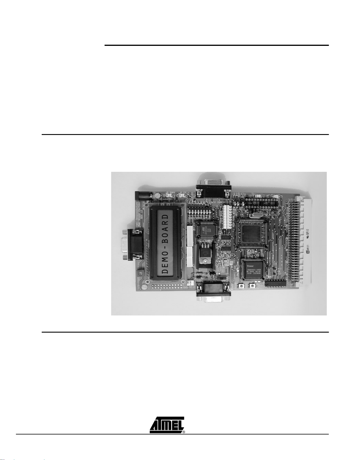
The C51/C251 Demo Board allows easy evaluation of most of Atmel C51/C251 devices.
The C51/C251 Demo Board can be powered using a simple 9V battery or using a 9V
rechargeable battery. The C51/C251 Demo Board can also be used as programming
tool for Flash products.
1.1 Package
Contents
n One PCB C51/C251 Demo Board (with battery connector)
n One Serial cable (1.8m length)
Figure 1-1. C51/C251 Demo Board
1.2 On-line Utilities The following utilies involved in using the C51/C251 Demo Board are available on the
Atmel Web site http://www.atmel.com.
Search for DEMOBOARD1.
n FLIP: In-System Programming (ISP) software for Flash microcontrollers
n ISP Demo Board Source and Code to program external Flash memory
n Source and Code of demo software
C51 Microcontrollers Demo Board User Guide 1-2
4119C–8051–3/03
Page 6

Introduction
1.3 Support Questions can be sent to: mcu@atmel.com
1.4 Demo Board Features
n An LCD Display (2 lines of 16 characters)
n An Eight LED Bar Graph
n 128 KB Flash Memory
n Three Different Sockets: PLCC44, PLCC68 & DIL24
n In-System Programming (ISP) Software to Download HEX Files in Flash Memory
n Hardware Capability to Program the Microcontrollers On-Chip Flash Memory
n Extension Connectors for Special Features, Applications, New Products, or Demos
1-3 C51 Microcontrollers Demo Board User Guide
4119C–8051–3/03
Page 7
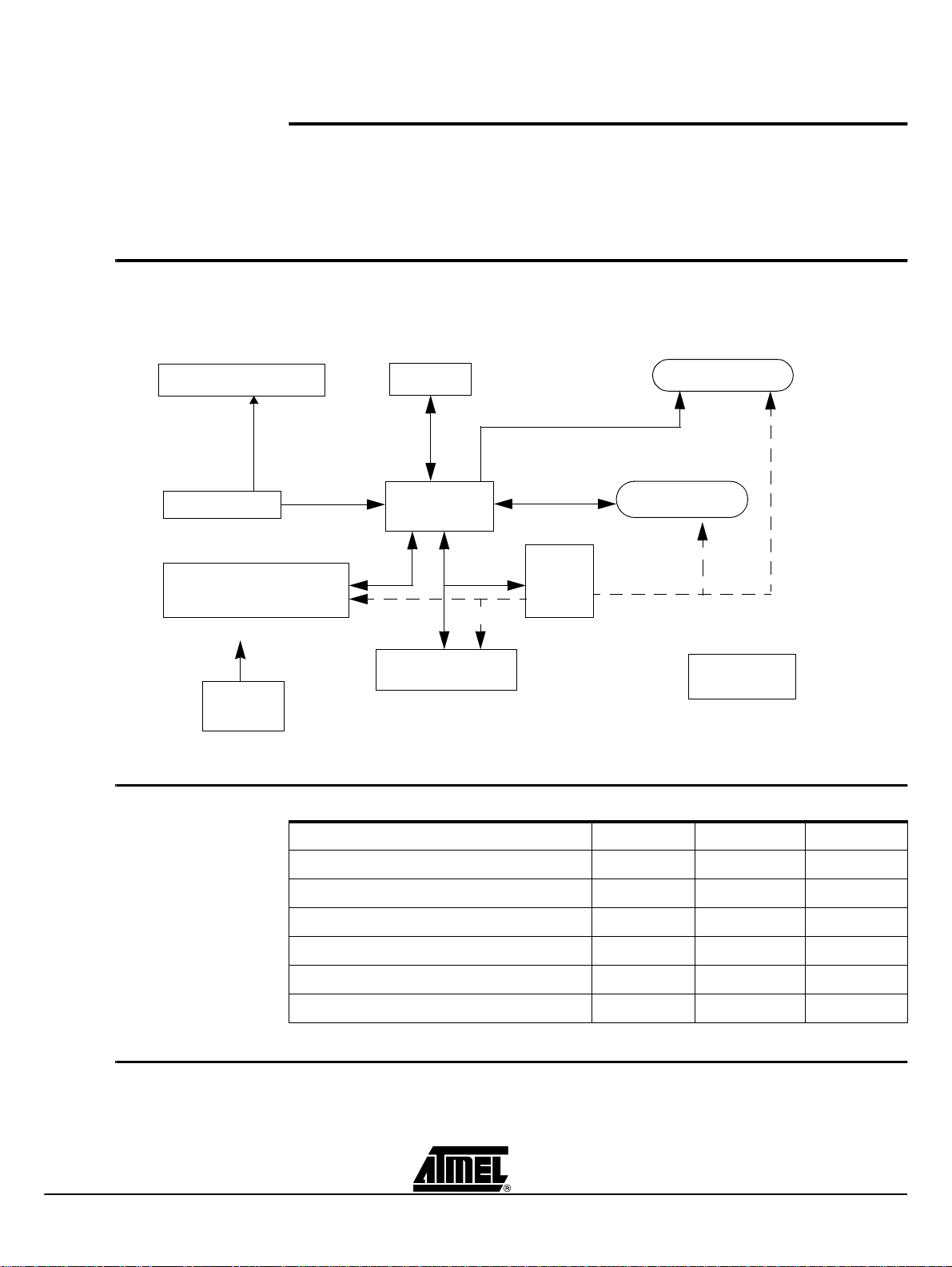
2.1 Block Diagr am
Figure 2-1. Block Diagram
Hardware Description
Section 2
Hardware Description
Synchro connectors
Reset & INT1#
128 K Flash memory
Power
interface
2.2 Specifications
RS232
C51/C251
Glue
To All
Parameter Typ Max Unit
Config switches
Bargraph
LCD 2*16
Extensions
connector
Supply DC voltage 9 12 V
Supply DC current 200 mA
Consumption at 12 MHz 60 100 mA
Consumption at 60 MHz in X2 mode 110 150 mA
non-rechargeable battery capacity 550 mAh
Rechargeable battery capacity 150 mAh
2.3 Supported Microcontrollers
C51 Microcontrollers Demo Board User Guide 2-4
Most Atmel C51 and C251 microcontrollers are supported.
The Demo Board does not support low voltage parts, only 5V parts are supported.
4119C–8051–3/03
Page 8
Hardware Description
2.4 Board Supply Considerations
Figure 2-2. C51/C251 Demo Board powered by J1 with a non-rechargeable battery on J2
n Power connector J1 or battery connector J2 may be used to power the board.
n On J2 connector a rechargeable battery or a non-rechargeable battery may be used.
n In case of rechargeable battery usage on J2, if J18 is ON the battery is charged when
the board is powered by J1.
n Board may be powered by J2 for about 10 hours with one new non-rechargeable
battery.
Note:
J18 must be Off, when the board is powered by J1 with a non-rechargeable
battery connected on J2 (see figure 3).
AC-DC
J1 Power Supply Connector
LCD display
J2
J18
9V to 12V DC IN
OFF
non-rechargeable
battery
9V
PP3
Figure 2-3. C51/C251 Demo Board powered by J1 with a rechargeable battery on J2
J1 Power Supply Connector
AC-DC
LCD display
J2
J18
9V to 12V DC IN
ON
rechargeable
battery
2-5 C51 Microcontrollers Demo Board User Guide
4119C–8051–3/03
9V
PP3
In this configuration
battery is being charged
Page 9
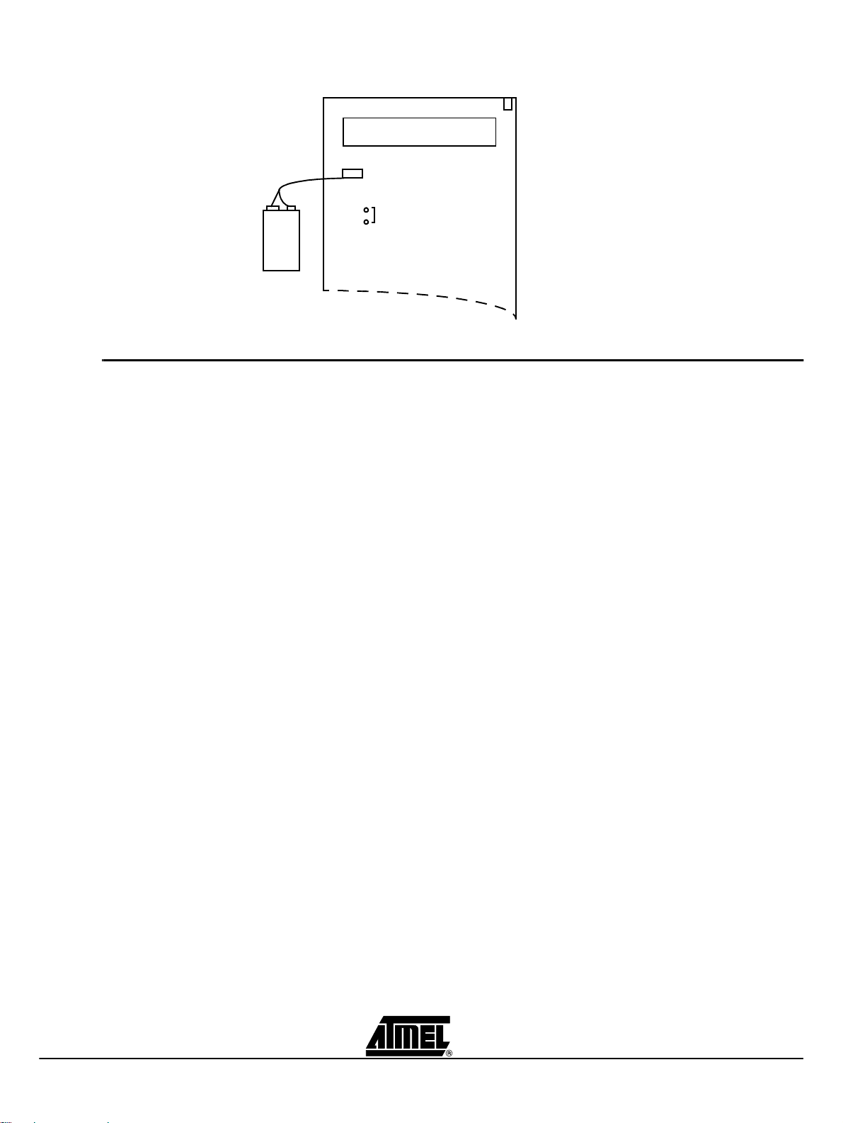
Figure 2-4. C51/C251 Demo Board Powered by J2.
J2
battery
(rechargeable or not)
9V
PP3
2.5 Board Layout n On-Off
– Switches ON the power supply.
n
Reset
– Resets the microcontroll ers.
LCD display
J18
ON
Hardware Description
J1 Power Supply Connector
NOT USED
n
INT1#
– Issues an interruption on microcontollers on INT1# pin.
n
J8 Connector
– Configure hardware in Page Mode or Non Page Mode.
– for C251 microcontrollers. For C51 products, the configuration must be set to
Non Page Mode.
n
Synchro IN
– Used to connect several C51/C251 Demo Boards together, provides global
reset / interrupt for all connected C51/C251 Demo Boards.
n
Synchro OUT
– Only one power supply is needed but it may be able to deliver enough
current to supply all the C51/C251 Demo Boards.
– There are no rules to connect two boards together anyone of the two DB9
may be used.
n
RS232
– Used to connect a terminal or through an RS232 serial communication port.
– This serial port can be used for displaying messages or for programming
external Flash memory.
Note: The cable that connect this RS232 Connector MUST be a pin to pin cable.
C51 Microcontrollers Demo Board User Guide 2-6
4119C–8051–3/03
Page 10

Hardware Description
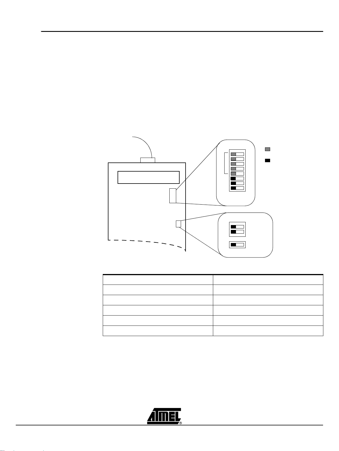
Figure 2-5. C51/C251 Demo Board
RS232 Cable to Terminal
R21
+
LCD CTRST
LCD
RS232
J11
Synchro IN
RESET
INT1
PLCC44
2.6 J11 Switches Table 1. J11 Switches
76543210
ISP ALE PSEN UC4 UC3 UC2 UC1 UC0
J17
X1
OFF
J8
ON
J9
J16
1
PLCC68
11
X2
X3
Synchro OUT
Page Mode
J8
Non Page Mode
DIL24
Extension connector
Bit
Number
7ISP1
6ALE
5PSEN
4-0 UC4:0
Bit
Mnemonic Description
In-System Programming (external Flash memory)
Set to enable external Flash memory programming
Clear to protect external Flash memory from erasure and programming
Address Latch Enable
Set to see ALE ac ti v i ty
Clear to ground ALE
Program Store Enable
Set to run demos
Clear to program T89C51RD2 on-chip Flash memory
User Code
Free of use as data input for demos.
(Set=1, Clear=0)
2-7 C51 Microcontrollers Demo Board User Guide
4119C–8051–3/03
Page 11

T able 2. J9 Switches
MAP SELECT EA
Hardware Description
10
Figure 2-6. Switch Configuration
Bit
Number
1
Bit
Mnemonic Description
MAP
SELECT
0EA
T able 3. J16 Switches
Bit
Number
0ISP2
Bit
Mnemonic Description
RS232 Cable to PC
Map Select
Set to select external Flash memory zone from $10000 to $1FFFF
Clear to select external Flash memory zone from $00000 to $0FFFF
External Address
Set to fetch internal code (on chip code).
Clear to fetch code from external Flash memory
0
ISP2
In System Programming 2 (external Flash memory)
RESERVED
MUST BE OFF (set to 1)
J11
J11
J16
User Code
PSEN
ALE
ISP1
1
J9
J9
OFF
10
0
7
0
EA
MAP SELECT
ISP2
Set = 1
Clear = 0
J16
Socket and Quartz Crystal The C51/C2 51 Demo Board provid es three different so ckets for microcontr ollers, a
PLCC44, a PLCC68 and a DIL24.
Each socket has it own quartz crystal X1, X2 and X3.
Only one Atmel mic rocontroller mu st be plugged-i n at one time, in one of the three
sockets.
Crystal may be easily changed on each socket.
C51 Microcontrollers Demo Board User Guide 2-8
4119C–8051–3/03
Page 12

Page 13

3.1 Flash Products
Operation Mode
Section 3
Operation Mode
3.1.1 Switch Configuration
To program the on-chip Flash memory, hardware configuration of the chip should be the
following: PSEN = 0, EA = 1 and ALE = 1 or not connected.
On C51/C251 Demo Board, switches must be as shown on Figure 3-2.
Figure 3-1. C51/C251 Demo Board Switches Configuration to use ISP
RS232 Cable to PC
J11
User Code
PSEN
J11
J9
J16
ALE
ISP1
J9
J16
1
10
Position don’t care
Position needed
0
EA
MAP SELECT
ISP2
3.1.2 Running ISP The C51/C251 Dem o Board m ust be co nnected to a PC com p ort via the RS232 cab le
connected to the RS232 connector of C51/C251 Demo Board.
After downloading, you can run code by switching PSEN on J11 to 1 and pressing the
RESET push button.
C51 Microcontrollers Demo Board User Guide 3-10
4119C–8051–3/03
Page 14
Operation Mode
3.2 ISP External Flash Memory Mode
3.2.1 Hardware Configuration
External Flash memory might be programmed using Windows hyper terminal or any terminal able to send HEX files in text mode.
The C51/C251 Demo Boar d mus t be conn ected to the P C com port w ith the cable connected to the RS232 connector J10.
The switch must be set as shown on Figure 3-2.
PLCC44 socket and X1 Quartz crystal will be used to program external Flash memory.
X1 must be 11.0592 Mhz and Atmel microcontroller must be plugged into PLCC44
socket.
Figure 3-2. C51/C251 Demo Board Switches Configuration to Program External Flash
Memory.
RS232 Cable to PC
J11
User Code
Position don’t care
Position needed
PSEN
J11
ALE
ISP1
1
0
3.2.2 Terminal Configuration
J9
J16
Use the following configuration for the terminal.
Parameter Value
Bauds 9600
Data bits 8
Stop bits 1
Parity None
Flow control Xon-Xoff
J9
J16
10
EA
MAP SELECT
ISP2
3.2.3 ISP Operation 1. Connect C51/C251 Demo Board to the PC com port with the cable.
2. Run Windows hyper terminal and configure it with the parameter specified in Figure 3-3.
3-11 C51 Microcontrollers Demo Board User Guide
4119C–8051–3/03
Page 15

Figure 3-3. Com Port Configuration
Operation Mode
Figure 3-4. Terminal Window on Running ISP
Turn on the C51/C251 Demo Board and then follow the instructions on the terminal
screen and LCD display. After eras ing Flash, the program asks for the mem ory zone,
and then asks to s end the HE X fil e i n text m ode (se e Fi gur e 3-4, Figure 3-5 & Fi gure 3-
6).
C51 Microcontrollers Demo Board User Guide 3-12
4119C–8051–3/03
Page 16

Operation Mode
Figure 3-5. Send HEX File in Text Mode
Figure 3-6. Use *.* in the Selection Zone to See HEX files in the Directory
3-13 C51 Microcontrollers Demo Board User Guide
4119C–8051–3/03
Page 17

Operation Mode
After the download of the HEX file, the program asks if you want to download another
HEX file in the second zone of the external Flash memory.
In this case you’ll have to switch MAP SELECT (to access second zone) and send
another HEX file in text mode.
All the external flash memory (128K byt es) is erased when ISP is used, ev en if yo u only
want to download one zone.
If you have one external F lash memor y zone p rogrammed, an d later you want to add
another program to the second memory zone, you will have to download both programs
at the same time.
Note: The data transfer is seen on bar graph.
3.3 Demo Mode In demo mode, programs stored into external flash memory are executed to demon-
strate capability of Atmel Microcontrollers. To run external code we must have EA=0.
In this mode the first four bits of J11 (UC3:0) are used to select demo program and UC4
is used to select display (LCD or RS232).
Figure 3-7. Switch Utilities in Demo Mode
J11
J11
J16
User Code
PSEN
ALE
ISP1
1
0
J9
J9
MAP SELECT
J16
10
Used to select demo program
Used to select display
EA
Used to select memory zone
ISP2
3.3.1 C51 Mode In C51 mode (Non Page Mode) switch J8 must be as shown in Figure 3-8.
C51 Microcontrollers Demo Board User Guide 3-14
4119C–8051–3/03
Page 18

Operation Mode
Figure 3-8. C51 Mode (Non Page Mode)
J11
J8
NON PAGE MODE
J9
J16
3.3.2 C251 Mode In C251 mode, the microcontroller can be used in Page Mode or Non Page Mode. For Non Page Mode switch J8 must be in the same configuration as in C51 mode. For Page Mode switch J8 must be as shown in Figure 3-9.
Figure 3-9. C251 Mode (Page Mode)
J11
PAGE MODE
J8
J9
J16
3-15 C51 Microcontrollers Demo Board User Guide
4119C–8051–3/03
Page 19

Section 4
Bill of Material
Reference Type Qty Comment
C1-C28 POL_CAPACITOR 4,7uF 2 CMS_TAJ_Package_B
C2:C10-C19:C23 CAPACITOR 100nF 14 Package_0805
C11 POL_CAPACITOR 3,3uF 1 TAJ_CMS_Package_B
C12 POL_CAPACITOR 10uF 1 TAJ_CMS_Package_B
C13-C14-C24:C27 CAPACITOR 22pF 6 Serie_680
C15:C18 POL_CAPACITOR 10uF 4 CMS_TAJ_Package_B
D1-D14 1N4001 1N4001 2 Package_DO204AL
D2-D11:D13 LED LED 4 CMS_STANDA R T
D3:D6 LED_GRE E N GREEN LED 1 in_line_2.54mm step
D7:D8 LED_YE L LOW YELLOW LED 1 in_line_2.54m m step
D9:D10 LED_R ED RED LED 1 in_line_2.54mm step
J1 CONNECTOR CONNECTOR 1
J2 CONNECTOR_BATTERY_9V CONN_BATTERY_9V 1
J3 STRAP STRAP 0
J4 DB9_MALE DB9_MALE 1 SUBD9Pins_Right_Angle
J5-J10 DB9_FEMELLE DB9_FEMELLE 2 SUBD9Pins_Right_Angle
J6:J7 Push_Button Push_Button 2 C MS
J8 SWITCH_ON_ON SWITCH_ON_ON 1
J9 Commut_DIP_2 Commut_DIP_2 1
J11 Commut_DIP_8 Commut_DIP_8 1 DIL
J12 CONNE C T O R CONNE CT OR 1 DIN41612_3*32_MALE_Right_Angle
J13 Jum pe r_2,54mm CONNECTOR 1 2 *11 con tac ts
J14 LCD_2X16 LCD_2X16 1 NULL
J15 ALE_DIS Strap 0
J16 Commut_DIP_1 Commut_DIP_1 1
J17 Switch ON-ON Switch ON-ON 1 Inter. ON/OFF
J18 jumper Battery Picot Pile 1 2 pins, ste p of 2,54mm
J19 Switch ON-ON Switch ON-ON
R1-R24-R28-R29 RESISTOR 1kOhm 4 Package_0603
R2-R3-R20-R21-R25:RESI STOR 10kOhm 6 Pa c kage_0603
R4:R11 RESISTOR 10kOhm 2 Package_1206-CMS _ARC_241
R12-R19 RESISTOR 1kOhm 2 Package_1206_CMS_ARC_241
R21 POTENTIOMETER 10kOhm 1 SERIE_3362P
R23 RESISTOR 100 Ohm 1 0.6W-1%
R30 RESISTOR 180 Ohm 1 0,5W
U1 LM7805C LM7805C 1 TO220 + Heat er
U2 LM2936Z5 LM2936Z5 1 TO92
U3-U4-U7-U8 74ACT573 74ACT573 4 CMS
U5 TSC80C31 Socket 1 PLCC44
U6 AT49HF010-45JC Sock et 1 PLCC32
U9 I C L232CBE ICL232CBE 1 CMS
U10 HEF4555P HEF4555P 1 DIL
U12 TSC80C51 Socket 1 DIL24
U13 TSC80C51 Socket 1 PLCC68
U14 74ACT14 74ACT14 1 CMS
U15 74ACT00 74ACT00 1 CMS
X1 Quartz_11.05920 11,0592 MHz 1 HC49/4H
X2 Quartz_22,1184 22,1184 MHz 1 HC49/U
Bill of Material
C51 Microcontrollers Demo Board User Guide 4-16
4119C–8051–3/03
Page 20

Page 21

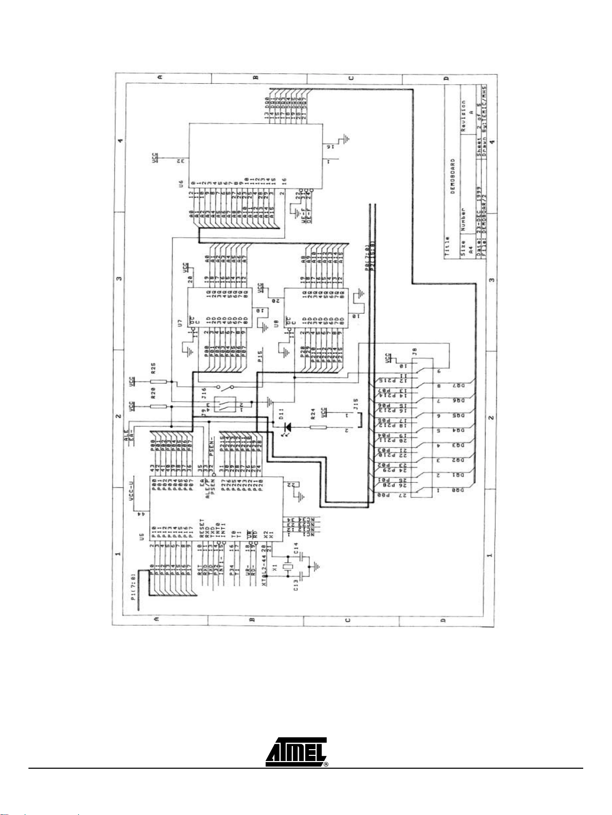
Section 5
Schematics
C51 Demo Board User Guide 5-18
Rev. 4119C–8051–3/03
Page 22
Schematics
5-19 C51 Demo Board User Guide
4119C–8051–3/03
Page 23

Schematics
C51 Demo Board User Guide 5-20
4119C–8051–3/03
Page 24

Schematics
5-21 C51 Demo Board User Guide
4119C–8051–3/03
Page 25

Schematics
C51 Demo Board User Guide 5-22
4119C–8051–3/03
Page 26

Schematics
5-23 C51 Demo Board User Guide
4119C–8051–3/03
Page 27

Atmel Headquarters Atmel Operations
Corporate Headquarters
2325 Orchard Parkway
San Jose, CA 95131
TEL 1(408) 441-0311
FAX 1(408) 487-2600
Europe
Atmel SarL
Route des Arsenaux 41
Casa Postale 80
CH-1705 Fribourg
Switzerland
TEL (41) 26-426-5555
FAX (41) 26-426-5500
Asia
Atmel Asia, Ltd.
Room 1219
Chinachem Gol den P laza
77 Mody Road Tsimhatsui
East Kowloon
Hong Kong
TEL (852) 2721-9778
FAX (852) 2722-1369
Japan
Atmel Japan K.K.
9F, Tonetsu Shinkawa Bldg.
1-24-8 Shin kawa
Chuo-ku, Tokyo 104-0033
Japan
TEL (81) 3- 3523-3 551
FAX (81) 3-3523-7581
Memory
Atmel Corporate
2325 Orchard Parkway
San Jose, CA 95131
TEL 1(408) 436-4270
FAX 1(408) 436-4314
Microcontrollers
Atmel Corporate
2325 Orchard Parkway
San Jose, CA 95131
TEL 1(408) 436-4270
FAX 1(408) 436-4314
Atmel Nantes
La Chantrerie
BP 70602
44306 Nantes Cedex 3, France
TEL (33) 2-40-18-18-18
FAX (33) 2- 40-18- 19-6 0
ASIC/ASSP/Smart Cards
Atmel Rousset
Zone Industrielle
13106 Rousset Cedex, France
TEL (33) 4-42-53-60-00
FAX (33) 4- 42-53- 60-0 1
Atmel Colorado Springs
1150 East Cheyenne Mtn. Blvd.
Colorado Springs, CO 80906
TEL 1(719) 576-3300
FAX 1(719) 540-1759
RF/Automotive
Atmel Heilbronn
Theresienstrasse 2
Postfach 3535
74025 Heilbro nn, Ge rmany
TEL (49) 71-31-67-0
FAX (49) 71-31-67-2340
Atmel Colorado Springs
1150 East Cheyenne Mtn. Blvd.
Colorado Springs, CO 80906
TEL 1(719) 576-3300
FAX 1(719) 540-1759
Biometrics/Imaging/Hi-Rel MPU/
High Speed Converters/RF Datacom
Atmel Grenoble
Avenue de Rochepleine
BP 123
38521 Saint-Egreve Cedex, France
TEL (33) 4-76-58-30-00
FAX (33) 4- 76-58- 34-8 0
Atmel Smart Card ICs
Scottish Enterprise Technology Park
Maxwell Building
East Kilbride G75 0QR, Scotland
TEL (44) 1355-803-000
FAX (44) 1355-242-743
e-mail
literature@atmel.com
Web Site
http://www.atmel.com
© Atmel Corporation 2003.
Atmel Corporation makes no warranty for the us e of its products, other than those expressly contained in the Company’s standard warr anty
which is detailed in Atmel’s Terms and Conditions located on the Company ’s web site. The Company assumes no responsibility for any e rrors
which may appear in this document, reserves the right to change devices or specifications detailed herein at any time w ithout notice, and does
not make any commitment to update the information contained herein. No licenses to patents or other intellectual property of Atmel are granted
by the Company in connection with the sale of Atmel products, expressly or by im plication. Atmel’s products are not authorized for use as critical
components in life support devices or systems.
Atmel® is a registered trademark of Atmel.
Other terms and product names may be the trademarks of others.
Printed on recycled paper.
4119C–8051–3/03
/xM
 Loading...