

Page 1
AVR2016: RZRAVEN Hardware User's Guide
Features
• Development kit for the AT86RF230 radio transceiver and AVR® microcontroller.
• CE, ETSI and FCC approved.
• LCD module (AVRRAVEN):
- AT86RF230 radio transceiver with high gain PCB antenna.
- Dual AVR microcontrollers.
- Dynamic Speaker and microphone.
- Atmel Serial Dataflash®.
- User IO section:
• USART
• GPIO
• Relay Driver
- Powered by battery or external supply:
• 5V to 12V external supply.
• USB module (RZUSBSTICK):
- AT86RF230 radio transceiver with miniature PCB antenna.
- AVR microcontroller with integrated Full Speed USB interface.
- External memory interface.
1 Introduction
8-bit
Microcontrollers
Application Note
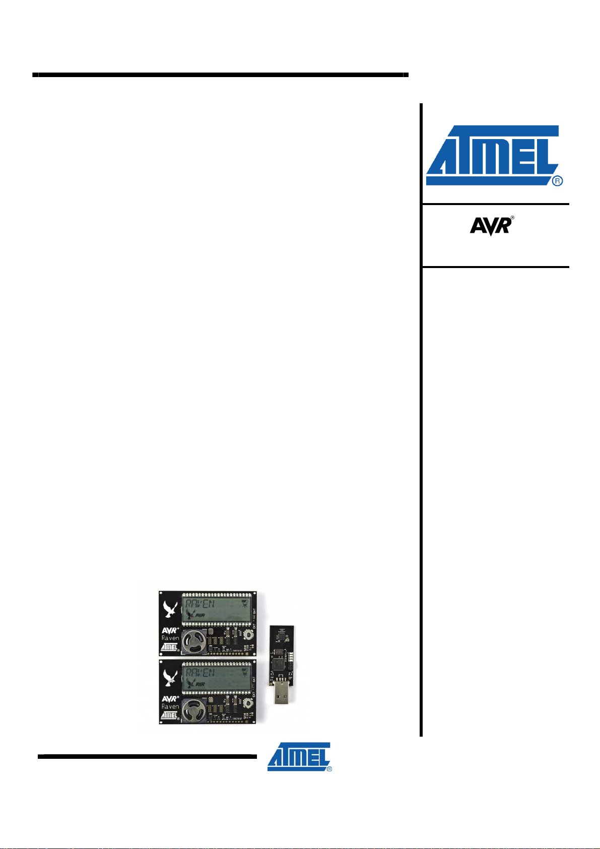
The RZRAVEN is a development kit for the AT86RF230 radio transceiver and the
AVR microcontroller. It serves as a versatile and professional platform for
developing and debugging a wide range of RF applications; spanning from: simple
point-to-point communication through full blown sensor networks with numerous
nodes running complex communication stacks. On top of this, the kit provides a
nice human interface, which spans from PC connectivity, through LCD and audio
input and output.
Figure 1-1. The RZRAVEN Kit Modules
Rev. 8117D-AVR-04/08
Page 2
2 General
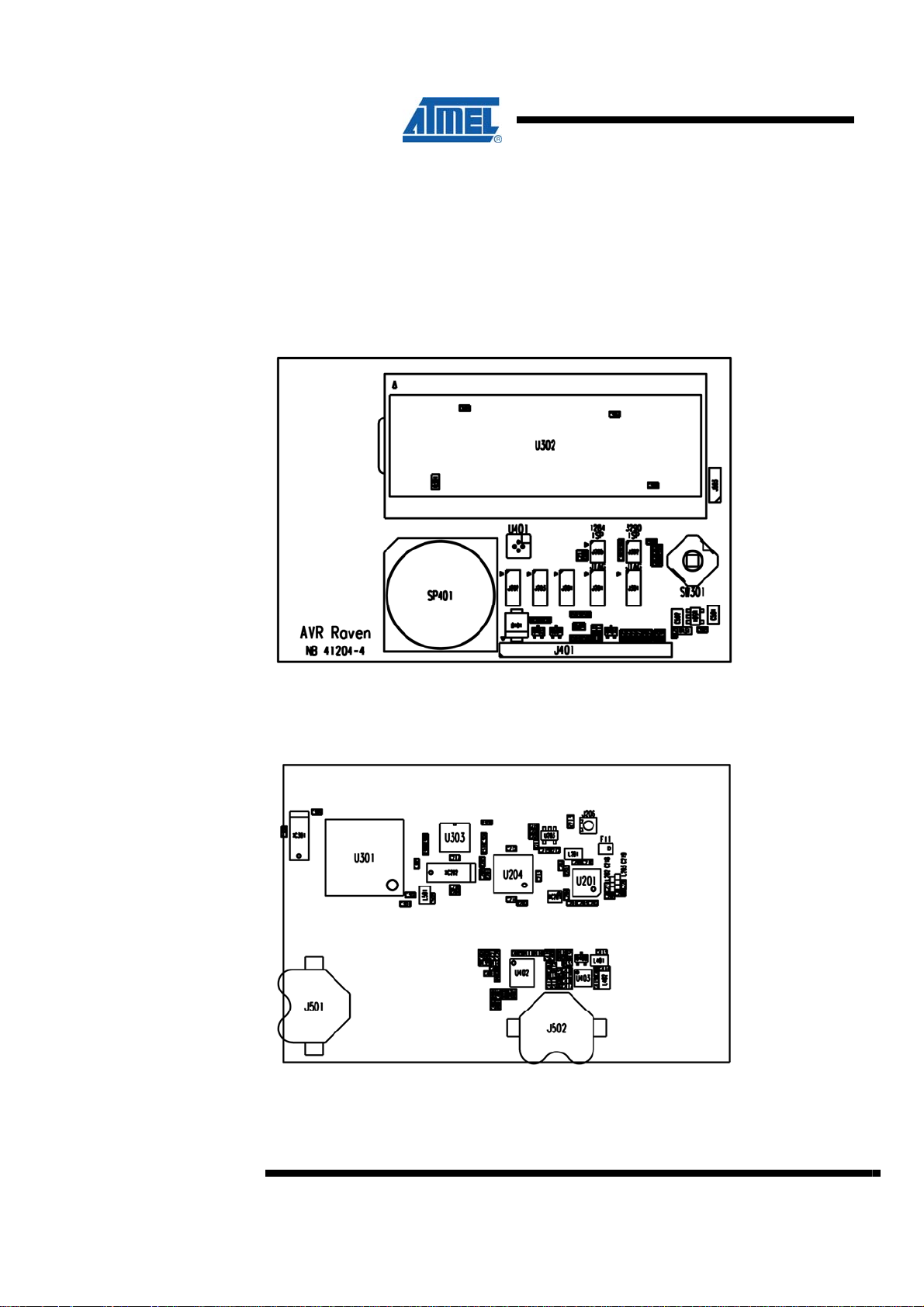
The RZRAVEN kit is built from one RZUSBSTICK module and two AVRRAVEN
modules. See
The complete schematics and Gerber files are available from the compressed archive
accompanying this application note.
Figure 2-1 Assembly drawing AVRRAVEN - front view.
Figure 2-1 to Figure 2-4 for further details.
Figure 2-2 Assembly drawing AVRRAVEN - back view.
2
AVR2016
8117D-AVR-04/08
Page 3
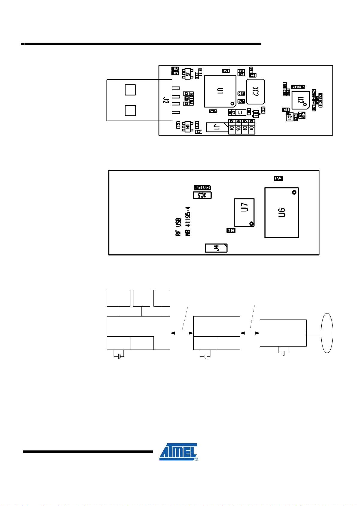
Figure 2-3 Assembly drawing RZUSBSTICK - front view.
Figure 2-4 Assembly drawing RZUSBSTICK - back view
AVR2016
3 The AVRRAVEN Module
Figure 3-1 AVRRAVEN overview
Joystick
and user
I/O
MCU #1:
ATmega3290P,
User I/O
Realtime
Clock oscillator
32kHz Xtal
The AVRRAVEN hardware is based on 2 microcontroller and one radio transceiver
chip. The ATmega3290P handles the sensors and the user interface and the
ATmega1284P handles the AT86RF230 radio transceiver and the RF protocol stacks.
The MCUs and the radio communicate via serial interfaces.
For hardware details please refer to Appendix A for the complete AVRRAVEN
schematics.
Audio
I/O
On-chip MCU
RC oscillator,
Set to 4MHz
LCD
display
2-way async
Serial comm
MCU #2:
ATmega1284P,
RF Stacks
Realtime
Clock oscillator
32kHz Xtal
On-chip MCU
RC oscillator,
Set to 4MHz
2-way sync
Serial comm
PCB Antenna
Radio chip
AT86RF230
16MHz Xtal
8117D-AVR-04/08
3
Page 4
3.1 AVR Microcontrollers
Two AVR microcontrollers are found on the AVRRAVEN module. An ATmega1284P
is connected to the AT86RF230 radio transceiver, and an ATmega3290P is driving
the LCD. Both these devices are selected from the AVR picoPower family, something
that ensures minimal power consumption and operation down to 1.8 Volts. Universal
Synchronous and Asynchronous serial Receiver and Transmitter (USART) is used as
an inter processor communication bus.
3.2 Atmel Radio Transceiver
The AT86RF230 is a 2.4GHz radio transceiver that is tailored for a wide range of
wireless applications. Low power consumption and market leading RF performance
makes it an excellent choice for virtually any type of networking device. Support for
IEEE 802.15.4
channel access) type of applications is available through an enhanced layer of
functionality on top of the basic radio transceiver.
3.3 Antenna description
The antenna on the AVRRAVEN is a 100 loop antenna with a net peak gain of
about 5dB.
3.4 LCD
TM
(Automatic acknowledge of packets, address filtering and automatic
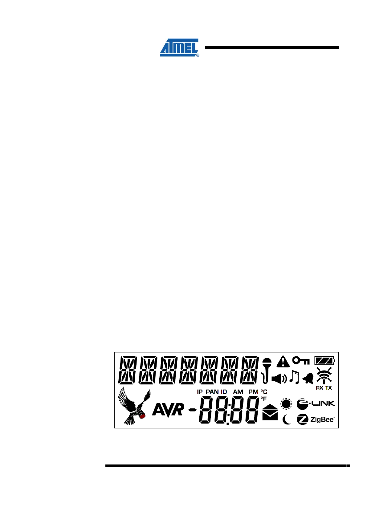
The LCD found on the AVRRAVEN module is a full custom 160-segment display
tailored for the RZRAVEN kit (See
segments text area; four segment number area and numerous handy symbols. In
particular pay attention to the bird looking symbol. It is symbolizing the two black
scouting ravens of Norse god Odin; Hugin (Thought) and Munin (Memory). The saga
says that they flew around the world and reported news back to Odin at night.
Underneath the raven segment’s “eye” there is a red LED capable of soft-blinking;
this may be used to indicate the AVRRAVEN’s search for “news” on the air interface.
A full segment map can be found in Appendix C and in the schematics folder in the
compressed archive file accompanying this application note. The LCD is driven
directly from the connected ATmega3290P.
Figure 3-2 AVRRAVEN - LCD Segments
Figure 3-2 for a quick reference). It contains a 7
4
AVR2016
8117D-AVR-04/08
Page 5

3.5 Speaker
3.6 Microphone
3.7 Serial Dataflash®
An 8 speaker is provided. The ATmega3290P controls all audio. The signal source
is the TIMER1’s PWM output and the signal is shaped via a low-pass filter and
amplified by a Class-D amplifier. Pulling PORTE7 low activates the active filter and
providing a PWM signal on PORTB5 activates the amplifier.
The AVRRAVEN’s microphone is connected to the ATmega3290P ADC channel 0.
The signal is amplified and low-pass filtered. Pulling PORTE7 low activates the
microphone circuit.
A 16-Mbits Atmel Serial Dataflash (AT45DB161D) is connected to the
ATmega3290P’s Serial Peripheral Interface (SPI). This storage is used for safe
firmware images, sounds and general-purpose parameters. See the firmware
documentation for an overview of occupied sectors, and those available to the end
user. Even with a couple of safe firmware images for the two microcontrollers there is
plenty space left for the end user. Please note that the serial Dataflash will operate
properly when the voltage is above 2.5 Volts while the rest of the design will operate
down to 1.8Volts
AVR2016
3.8 Serial EEPROM
3.9 Real Time Clock
3.10 NTC
A 2-Kbits Atmel Serial EEPROM (AT24C02B) is connected to the ATmega1284P’s
two-wire interface (TWI). This storage is write protected by hardware and can only be
read. The storage contains important configuration and calibration data that should
not be unintentionally overwritten. Information such as a unique EUI 64-bit address
can be found her-in. A rich set of access functions and the parameter map is given in
the RZRAVEN firmware documentation.
Separate 32768 Hz clock crystals are connected to the ATmega3290P’s and the
ATmega1284P’s asynchronous timer interfaces. This allows an application to
implement a real time clock (RTC) to keep track of time when sleep modes are used
to reduce the power consumption. This is especially important for battery-operated
nodes.
A NTC is connected to the ATmega3290P’s Analog to Digital Converter (ADC)
channel 4. This NTC can be used to measure the temperature in the surroundings of
the AVRRAVEN. The NTC can be found below the joystick, close to J401. The JTAG
interface must be disabled when using the temperature sensor. When running the
AVRRAVEN from an external power source the onboard voltage regulator may heat
the temperature sensor giving faulty reading. To avoid this the sensor NTC may be
soldered off and relocated using short wires. If a higher level of accuracy is required
the users may also calibrate the sensor by adjusting the temperature lookup table in
firmware.
8117D-AVR-04/08
5
Page 6
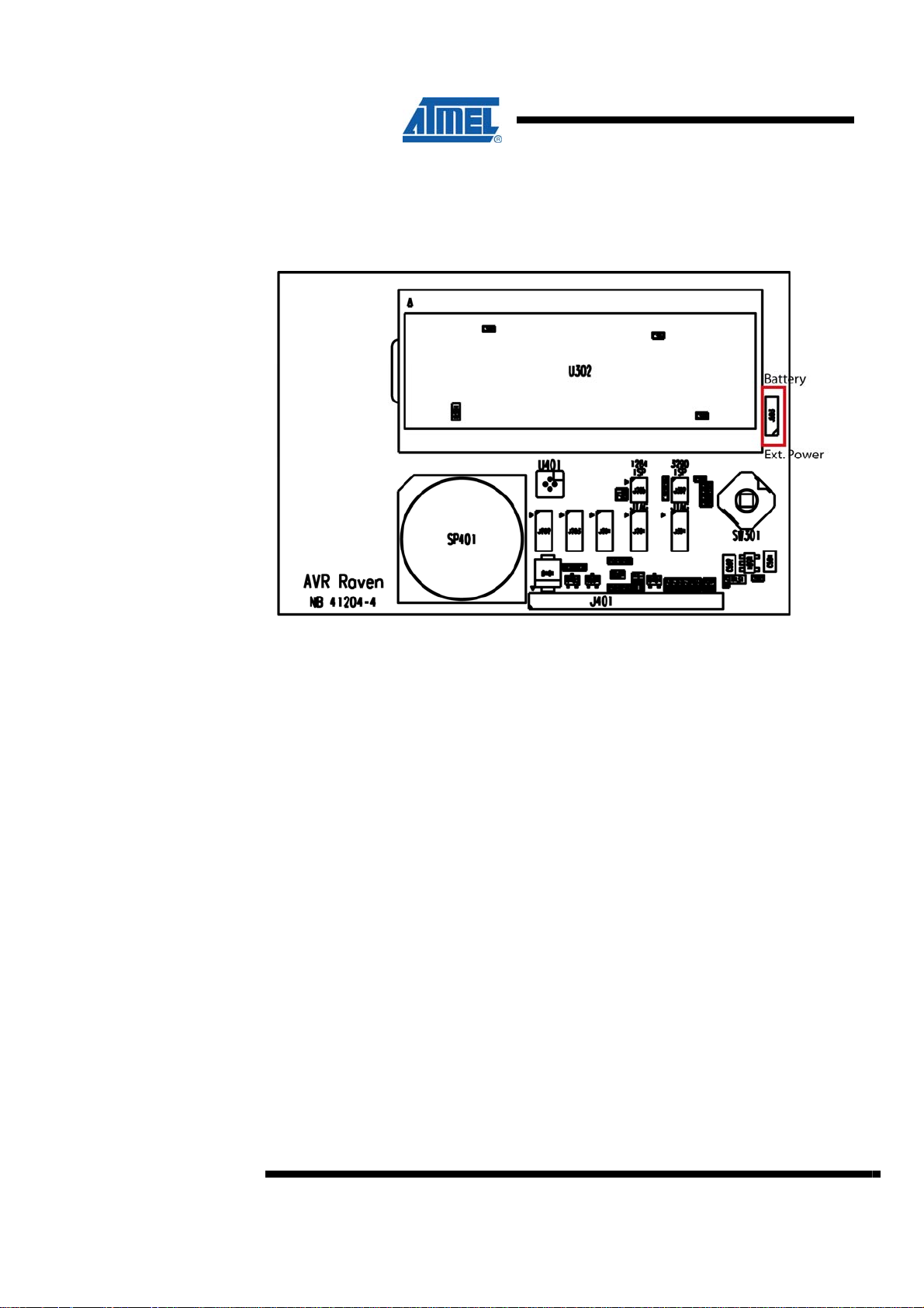
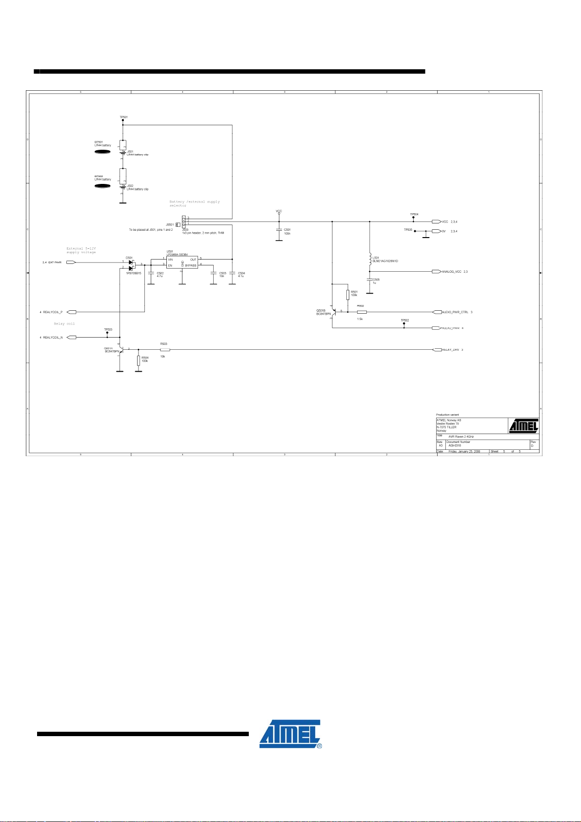
3.11 Power Supply
The AVRRAVEN can be powered either from batteries or an external 5 to 12 Volts
DC source. The power source is selected by the position of the jumper located
immediately to the right of the LCD (See the figure below for a reference). Polarity
protection is provided when using an external power source.
The AVRRAVEN has been designed to run from two 1.5V LR44 battery cells.
An onboard voltage regulator makes it possible to run power the AVRRAVEN from a
5 to 12 Volts DC source. The external voltage is applied to the two leftmost pins in the
user IO area (J401). The ATmega3290P’s ADC channel 2 is connected to a voltage
divider and the external voltage supply interface. This way it is possible for the
application to monitor the external operating voltage.
6
AVR2016
8117D-AVR-04/08
Page 7
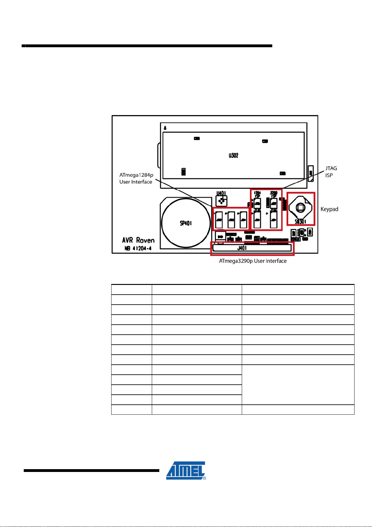
3.12 Interfaces
AVR2016
The AVRRAVEN module has multiple interfaces that can be used for serial
communication, interaction with external sensors and control units such as relays and
of course programming and debugging.
Figure 3-3 AVRRAVEN User Interfaces
Table 3-1
Pin number Function Comment
1 Ext. power supply, 5-12V input External power input
2 Ext. power supply 0V Connected to internal 0V
3 Relay coil positive Relay driver circuit positive
4 Relay coil negative Relay driver circuit negative
5 Voltage measure input, 0-Vcc*5 Analog input via 47k/10k voltage divider
6 Voltage measure input, 0-Vcc Analog input directly to ADC input.
7 Vcc Connected to the VCC net directly
8 User IO #1
9 User IO #2
10 User IO #3
11 User IO #4
12 Common Connected to internal 0V
. Interfaces available on J401
Digital I/O, may interface an LED or a
switch directly. On-board 470 series
resistors and 10k pull-ups are provided.
Pin change interrupts, TWI and USI is
also available on these pins.
Care should be taken when connecting to the AVRRAVEN’s interfaces, since there is
no protection circuitry provided. Damage to the MCUs or other circuits may be the
result of ESD spark, short circuits, polarity or over-voltage faults.
8117D-AVR-04/08
7
Page 8
3.12.1 Programming Interface
Both the ATmega3290P and ATmega1284P can be programmed using either the
JTAG or ISP interface. JTAG programming can be facilitated by connecting a JTAG
ICE mkII to the 50-mil pin header J301 (ATmega3290P) and J204 (ATmega1284P). A
total of 5 50-mil pin headers and one 50-mil to 100-mil converter are supplied with the
RZRAVEN kit.
ISP programming can be performed by connecting an ISP enabled AVR programming
tool to the pin header J302 (ATmega3290P) and J205 (ATmega1284P). AVR tools
like STK500, AVRISP mkII and JTAGICE mkII can be used for this.
The AVRRAVEN does not come with these headers mounted. So it is up to the user
populating these. Wires could also be soldered in instead of the dual row headers.
3.12.2 Relay Interface
A relay interface (Relay Positive and Negative) is available through J401. This
interface can be used with the AVRRAVEN running from external power. A switching
transistor is connected to PB6 on the ATmega3290P so that sufficient current can be
provided to the relay being driven. An external power source must be used if the relay
option is required. The AVRRAVEN must then be supplied with the rated voltage of
the relay.
3.13 Voltage Measurement Interface
3.13.1 GPIO
8
AVR2016
Two of the pins in header J401 can be used for external voltage measurements,
however only one at the time. The possible voltage ranges are 0 to VCC or via a
voltage divider giving an approximate range of 0 to five times VCC. A simple voltage
divider is implemented to scale the measurement voltage. A diode bridge is also used
to prevent reverse polarity and to protect the ATmega3290P’s ADC channel 3.
Both the ATmega3290P and ATmega1284P are high pin count devices, and a
number of these are not used. These pins are available through the user IO headers;
J401, J201, J202 and J203. See
Table 3-2 and Table 3-3 for further details.
Be aware that these pins do not have level converters and should thus not be
connected directly to an application board running on a different voltage level than the
AVRRAVEN.
Table 3-2
ATmega3290P Port Pin PCB Connection Comment
PE3 J401 –8
PE4 J401-9
PE5 J401-10
PE6 J401-11
. ATmega3290P User IO
Via 470 series resistor
and10k pull-up
Via 470 series resistor
and10k pull-up
Via 470 series resistor
and10k pull-up
Via 470 series resistor
and10k pull-up
8117D-AVR-04/08
Page 9
AVR2016
Table 3-3. ATmega1284P User IO
ATmega1284P Port Pin PCB Connection Comment
PC0 J201-1
PC1 J201-2
PC2 J201-3 JTAG TCK.
PC3 J201-4 JTAG TMS.
PC4 J201-5 JTAG TDO.
PC5 J201-6 JTAG TDI.
N.C. J201-7
N.C. J201-8
PD0 J202-1
PD1 J202-2
PD2 J202-3 DIO or RXD1.
PD3 J202-4 DIO or TXD1.
PD4 J202-5 DIO.
PD5 J202-6 DIO.
PB2 J202-7 DIO. NB: NOT PD6!
PD7 J202-8 DIO.
PA0 J203-1 DIO or ADC Channel 0.
PA1 J203-2 DIO or ADC Channel 1.
PA2 J203-3 DIO or ADC Channel 2.
PA3 J203-4 DIO or ADC Channel 3.
PA4 J203-5 DIO or ADC Channel 4.
PA5 J203-6 DIO or ADC Channel 5.
PA6 J203-7 DIO or ADC Channel 6.
PA7 J203-8 DIO or ADC Channel 7.
Additional interfaces PCB Connection Comment
External power J201-10
J202-10
J203-10
0V J201-9
J202-9
J203-9
TWI SCL.
Connected to serial EEPROM
TWI SDA.
Connected to serial EEPROM
Populate R204 to connect to
PC6. RTC Xtal XC202 must
then be removed.
Populate R205 to connect to
PC6. RTC Xtal XC202 must
then be removed.
RXD0 Inter processor
communication.
TXD0 Inter processor
communication.
Connected to J401-1
Connected to J401-2
8117D-AVR-04/08
9
Page 10

4 The AVR RZUSBSTICK Module
Figure 4-1 RZUSBSTICK overview
USB interface
MCU:
AT90USB1287,
USB and RF Stacks
MCU oscillator
2-way sync
Serial comm
Radio chip
AT86RF230
The AVR RZUSBSTICK hardware is based a USB microcontroller and a radio
transceiver chip. The AT90USB1287 microcontroller handles the USB interface, the
AT86RF230 radio transceiver and the RF protocol stacks.
For hardware details please refer to Appendix D for the complete AVR RZUSBSTICK
schematics.
4.1 AVR Microcontroller
The AT90USB1287 is a device in the family of AVRs with a low and full speed USB
macro with device, host and On-the-go (OTG) capabilities.
4.2 Atmel Radio Transceiver
The AT86RF230 is a 2.4GHz radio transceiver that is tailored for a wide range of
wireless applications. Low power consumption and market leading RF performance
makes it an excellent choice for virtually any type of networking device. Support for
IEEE 802.15.4 (Automatic acknowledge of packets, address filtering and automatic
channel access) type of applications is available through an enhanced layer of
functionality on top of the basic radio transceiver.
4.3 Antenna description
8MHz Xtal
16MHz Xtal
10
The antenna on the RZUSBSTICK is a folded dipole antenna with a net peak gain of
0dB
AVR2016
8117D-AVR-04/08
Page 11

4.4 Interfaces
Figure 4-2 RZUSBSTICK Interfaces - front.
Figure 4-3 RZUSBSTICK Interfaces - back
AVR2016
4.4.1 External Memory Interface
4.4.2 Serial Interface
When necessary the AT90USB1287’s 8k Bytes of internal SRAM can be extended
through the AVR external memory interface. The suggested external SRAM is 32k
Bytes and is available from address 0x8000 to 0xFFFF giving a total of 40k Bytes
when assembled.
Suggested latch and RAM:
• 74AHC573PW.
• BS62UV256TCP-10
The USART on the AT90USB1287 is routed to J4 on the RZRAVEN’s backside. J4 is
implemented as three large pads (RX-TX-GND) where the user can solder in wires
and route the signal to his or her preference. The RX-TX signals are TTL level, so an
external level converter must be connected if RS232 levels are necessary.
.
11
8117D-AVR-04/08
Page 12

4.4.3 Programming Interface
4.4.4 LEDs
A JTAG interface is provided for the AT90USB1287 microcontroller. The interface is
available through a 50-mil spaced 10-pin dual row header. The RZRAVEN does not
come with the header mounted. So it is up to the user populating it. Wires could also
be soldered in instead of the dual row headers. A total of 5 50-mil pin headers and
one 50-mil to 100-mil converter are supplied with the RZRAVEN kit.
4 LEDs is assembled on the board:
Table 4-1
LED AT90USB1297 Port Pin Comment
Blue (D1) PORTD7 Turn LED on by pulling port pin high
Red (D2) PORTD5 Turn LED on by pulling port pin low
Green (D3) PORTE7 Turn LED on by pulling port pin low
Orange (D4) PORTE6 Turn LED on by pulling port pin low
. AT90USB1287 LEDs
12
AVR2016
8117D-AVR-04/08
Page 13

5 Appendix A: AVRRAVEN Schematics
AVR2016
8117D-AVR-04/08
13
Page 14

14
AVR2016
8117D-AVR-04/08
Page 15

AVR2016
15
8117D-AVR-04/08
Page 16

16
AVR2016
8117D-AVR-04/08
Page 17
AVR2016
17
8117D-AVR-04/08
Page 18

6 Appendix B: AVRRAVEN Bill of materials
Table 6-1. AVRRAVEN BOM
Qty Designator Description Manufacturer Part #
C205, C206,
5
C207, C220,
C221
2 C201, C204
C413, C414,
3
C415
1 C404
C208, C301,
14
C405, C407,
C408, C409,
C410, C411,
C412, C416,
C417, C420,
C421, C503
2 C502, C504
C211, C212,
12
C213, C214,
C215, C303,
C304, C305,
C306, C307,
C418, C501
C202, C203,
10
C209, C210,
C302, C401,
C402, C403,
C406, C505
R201, R208,
4
R209, R415
R203, R306,
7
R425, R427,
R428, R430,
R434
R303, R401,
5
R404, R405,
R417
1 R502
R304, R411,
7
R412, R413,
R414, R432,
R435
Ceramic capacitor, SMD
0402, NP0, 50V, +/-
0.25pF
Ceramic capacitor, SMD
0402, NP0, 50V, +/-5%
Ceramic capacitor, SMD
0402, NP0, 50V, +/-10%
Ceramic capacitor, SMD
0402, X7R, 25V, +/-10%
Ceramic capacitor, SMD
0402, X7R, 25V, +/-10%
Ceramic capacitor, SMD
0805, Y5V, 10V, -20/+80
%
Ceramic capacitor, SMD
0402, X7R, 16V, +/-10%
Ceramic capacitor, SMD
0402, X5R, 6.3V, +/-10%
Thick film resistor, SMD
0402, 1/16W, 1%
Thick film resistor, SMD
0402, 1/16W, 1%
Thick film resistor, SMD
0402, 1/16W, 1%
Thick film resistor, SMD
0402, 1/16W, 1%
Thick film resistor, SMD
0402, 1/16W, 1%
1.2p
12p
100p
4.7n
10n
4.7u
Kemet C0402C104K4RACTU
Kemet C0402C105K9PAC
0R
470R
1k
1.5k
3k
18
AVR2016
8117D-AVR-04/08
Page 19

Qty Designator Description Manufacturer Part #
1 R410
R202, R206,
17
R210, R211,
R212, R301,
R302, R307,
R402, R406,
R407, R408,
R421, R422,
R423, R424,
R503
1 R305
R308, R309,
10
R310, R409,
R416, R419,
R426, R429,
R501, R504
R403, R418,
3
R420
1 R431
2 L401, L402 SMD RF inductor 0805 Murata BLM21PG300SN1D
2 L201, L501 SMD RF inductor 0805. Murata BLM21AG102SN1D
2 L202, L203
D401, D403,
3
D408
1 D501 Dual Schottky diode, Philips 1PS70SB15
1 D404
1 Q501
1 U303
1 U201
1 U203
1 U501
1 U402 LMV934MT 1V8 Quad
1 U204 AVR 8-bit RISC MCU ATMEL ATmega1284PV-10MU
1 U301 AVR 8-bit RISC MCU ATMEL ATmega3290PV-10AU
Thick film resistor, SMD
0402, 1/16W, 1%
Thick film resistor, SMD
0402, 1/16W, 1%
Thick film resistor, SMD
0402, 1/16W, 1%
Thick film resistor, SMD
0402, 1/16W, 1%
Thick film resistor, SMD
0402, 1/16W, 1%
NTC Thermistor
100kOhm
RF Inductor, 2.7nH,
0,17ohm, 300mA, 0402
Dual schottky diode, ST BAT54SWFILM
Bidirectional Transient
suppression diode, 600W
General purpose SMD
BJT dual NPN-PNP
16-megabit 2.7-3.6 volt
DataFlash
2.4GHz ZigBee/802.15.4
tranceiver
2kbit Serial (TWI)
EEPROM, AT24C02B,
1.8-5V
LDO 3.3V 150mA SOT235 (cer. cap)
3.3k
10k
47k
100k
470k
Murata NCP18WF104J03RB
Johanson
Technology
ST SM6T12CA
Philips BC847BPN
ATMEL AT45DB161D-SU
ATMEL AT86RF230-ZU
ATMEL AT24C02B-TSU-T
Texas Instruments LP2985A-33DBV
National
Semiconductor
AVR2016
L-07C2N7SV6T
LMV934MT
8117D-AVR-04/08
19
Page 20

Qty Designator Description Manufacturer Part #
1 U403
2 XC202, XC301
1 SP401
1 XC201
1 U401
1 SW301
1 PCB101 AVRRAVEN PCB A08-0402
2 J501, J502 LR44 battery clip, SMD Keystone Corp. 2996TR
1 J503
1 JS501
2 BT501, BT502 LR44 coin-cell battery
1 D301 LED, Red, SMD 0603 Lumex SML-LX0603SRW-TR
1 U302 AVRRAVEN LCD Orient Display 0710091B
TS2007 3W class D audio
amp.
32.768kHz SMD crystal,
85SMX style
PC board speaker, SMD
mount
16MHz uXtal GSX-323,
2.0 x 2.5 mm SMD 10ppm
Citizen 4.2x4.2mm SMD
electmic
ALPS 4-directional switch
with center push function
1x3 pin header, 2 mm
pitch, THM
Jumper cap for 2.00mm
pinheader
ST TS2007IQT
Rakon Ltd LF XTAL016207
Veco Vansonic 20CS08KQ-150ND
Golledge GSX-323/111BF 16.0MHz
Citizen CHM-04C-03
ALPS SKRHABE010
SAMTEC TMM-103-01-L-S
SAMTEC 2SN-BK-G
7 Appendix C: AVRRAVEN LCD
Figure 7-1 AVRRAVEN Segments
20
AVR2016
8117D-AVR-04/08
Page 21

AVR2016
Table 7-1. LCD Segment description and mapping
Bit
Registers 7 6 5 4 3 2 1 0 COM
LCDDR19
LCDDR18
LCDDR17
LCDDR16
LCDDR15
LCDDR14
LCDDR13
LCDDR12
LCDDR11
LCDDR1
LCDDR9
LCDDR8
LCDDR7
LCDDR6
LCDDR5
LCDDR4
LCDDR3
LCDDR2
LCDDR1
LCDDR0
SEG39 SEG38 SEG37 SEG36 SEG35 SEG34 SEG33 SEG32
8A 8B 9A 9B 10A 10B 11A 11B
SEG31 SEG30 SEG29 SEG28 SEG27 SEG26 SEG25 SEG24
PAN ID RX R1 B1 7C SPK 7M 7D
SEG23 SEG22 SEG21 SEG20 SEG19 SEG18 SEG17 SEG16
6C TONE 6M 6D 5C BELL 5M 5D
SEG15 SEG14 SEG13 SEG12 SEG11 SEG10 SEG9 SEG8
4C °C 4M 4D 3C °F 3M 3D
SEG7 SEG6 SEG5 SEG4 SEG3 SEG2 SEG1 SEG0
2C PM 2M 2D 1C AM 1M 1D
SEG39 SEG38 SEG37 SEG36 SEG35 SEG34 SEG33 SEG32
8F 8G 9F 9G 10F 10G 11F 11G
SEG31 SEG30 SEG29 SEG28 SEG27 SEG26 SEG25 SEG24
IP SUN TX B4 7H 7N 7L 7E
SEG23 SEG22 SEG21 SEG20 SEG19 SEG18 SEG17 SEG16
6H 6N 6L 6E 5H 5N 5L 5E
SEG15 SEG14 SEG13 SEG12 SEG11 SEG10 SEG9 SEG8
4H 4N 4L 4E 3H 3N 3L 3E
SEG7 SEG6 SEG5 SEG4 SEG3 SEG2 SEG1 SEG0
2H 2N 2L 2E 1H 1N 1L 1E
SEG39 SEG38 SEG37 SEG36 SEG35 SEG34 SEG33 SEG32
8E 8C 9E 9C 10E 10C 11E 11C
SEG31 SEG30 SEG29 SEG28 SEG27 SEG26 SEG25 SEG24
MINUS E1 Z-LINK B3 7B 7K 7J 7G
SEG23 SEG22 SEG21 SEG20 SEG19 SEG18 SEG17 SEG16
6B 6K 6J 6G 5B 5K 5J 5G
SEG15 SEG14 SEG13 SEG12 SEG11 SEG10 SEG9 SEG8
4B 4K 4J 4G 3B 3K 3J 3G
SEG7 SEG6 SEG5 SEG4 SEG3 SEG2 SEG1 SEG0
2B 2K 2J 2G 1B 1K 1J 1G
SEG39 SEG38 SEG37 SEG36 SEG35 SEG34 SEG33 SEG32
8D COLON 9D POINT 10D E3 11D E2
SEG31 SEG30 SEG29 SEG28 SEG27 SEG26 SEG25 SEG24
RAVEN+AVR MOON Z_ZIGBEE B2 MIC 7A 7I 7F
SEG23 SEG22 SEG21 SEG20 SEG19 SEG18 SEG17 SEG16
ATT! 6A 6I 6F KEY 5A 5I 5F
SEG15 SEG14 SEG13 SEG12 SEG11 SEG10 SEG9 SEG8
R5 4A 4I 4F R4 3A 3I 3F
SEG7 SEG6 SEG5 SEG4 SEG3 SEG2 SEG1 SEG0
R3 2A 2I 2F R2 1A 1I 1F
COM3
COM2
COM1
COM0
8117D-AVR-04/08
21
Page 22

8 Appendix D: RZUSBSTICK Schematics
22
AVR2016
8117D-AVR-04/08
Page 23

9 Appendix E: RZUSBSTICK Bill of materials
Table 9-1. RZUSBSTICK BOM
Qt Designator Description Manufacturer Part #
Ceramic capacitor, SMD
1 C18
2 C11, C12
2 C22, C23
2 C5, C6
2 C2, C8
1 C4
C1,C10,C13,C16,
C17,C21,C24, C25,
12
C26, C3, C7, C9
2 R15, R16
2 R3, R8
5 R1,R10,R5,R6,R7
R12, R13, R14, R2,
R4, R9
6
1 L1 SMD RF inductor 0805. Murata BLM21AG102SN1D
1 Q1 General purpose NPN. Philips BC847W
1 U5 Transient Suppressor, TI SN65220YZBR
1 U1
1 U2
1 U3
1 U4 LDO 3.3V 150mA TI LP2985A-33DBV
1 XC1 16MHz uXtal GSX-323, Golledge GSX-323/111BF 16.0MHz
1 XC2 8.0MHz Xtal GSX-752 Golledge GSX-752B/551EF 8MHz
1 PCB1 RZUSBStick PCB ATMEL A08-0384
1 J2 USB type A plug, SMD SAMTEC USB-AM-S-F-B-SM1-R
1 D2 LED, Red, Everlight EL17-21USRC
1 D3 LED, Green, Everlight EL17-21SYGC
1 D4 LED, Yellow, Everlight EL17-21UYC/A2
1 D1 LED, Blue, Everlight EL17-21UBC
0402, NP0, 50V, +/-.25pF
Ceramic capacitor, SMD
0402, NP0, 50V, +/-5%
Ceramic capacitor, SMD
0402, NP0, 50V, +/-5%
Ceramic capacitor, SMD
0402, NP0, 50V, +/-5%
Ceramic capacitor, SMD
0402, X7R, 25V, +/-10%
Ceramic capacitor, SMD
0402, X7R, 16V, +/-10%
Ceramic capacitor, SMD
0402, X5R, 6.3V, +/-10%
Thick film resistor, SMD
0402, 1/16W, 1%
Thick film resistor, SMD
0402, 1/16W, 1%
Thick film resistor, SMD
0402, 1/16W, 1%
Thick film resistor, SMD
0402, 1/16W, 1%
AVR 8-bit RISC MCU with
USB, QFN64 package
2.4GHz ZigBee/802.15.4
tranceiver
2kbit Serial (TWI)
EEPROM, AT24C02B,
1.5p
12p
18p
22p
10n
Kemet C0402C104K4RACTU
Kemet C0402C105K9PAC
0R
22R
470R
10k
ATMEL AT90USB1287-16MU
ATMEL AT86RF230-ZU
ATMEL AT24C02B-TSU-T
AVR2016
8117D-AVR-04/08
23
Page 24

10 Appendix F: Federal Communications Commission (FCC) Statement
10.1 FCC Statements
10.1.1 Equipment usage
This equipment is for use by developers for evaluation purposes only and must not be
incorporated into any other device or system.
10.1.2 Compliance Statement (Part 15.19)
These devices comply with Part 15 of the FCC Rules. Operation is subject to the
following two conditions:
1. These devices may not cause harmful interference, and
2. These devices must accept any interference received,
including interference that may cause undesired operation.
10.1.3 Warning (Part 15.21)
Changes or modifications not expressly approved by Atmel Norway could void the
user’s authority to operate the equipment.
10.1.4 Compliance Statement (Part 15.105(b) )
This equipment has been tested and found to comply with the limits for a Class B
digital device, pursuant to Part 15 of the FCC Rules. These limits are designed to
provide reasonable protection against harmful interference in a residential installation.
This equipment generates, uses and can radiate radio frequency energy and, if not
installed and used in accordance with the instructions, may cause harmful
interference to radio communications. However, there is no guarantee that
interference will not occur in a particular installation. If this equipment does cause
harmful interference to radio or television reception, which can be determined by
turning the equipment off and on, the user is encouraged to try to correct the
interference by one or more of the following measures:
- Reorient or relocate the receiving antenna.
- Increase the separation between the equipment and receiver.
- Connect the equipment into an outlet on a circuit different from that to which the
receiver is connected.
- Consult the dealer or an experienced radio/TV technician for help.
10.1.5 FCC IDs
The AVRRAVEN has FCCID: VW4AVRRAVEN
The RZUSBSTICK has FCCID: VW4AVRRZUSBSTICK
24
AVR2016
8117D-AVR-04/08
Page 25

11 Table of Contents
AVR2016
Features............................................................................................... 1
1 Introduction......................................................................................1
2 General .............................................................................................2
3 The AVRRAVEN Module..................................................................3
3.1 AVR Microcontrollers........................................................................................... 4
3.2 Atmel Radio Transceiver ..................................................................................... 4
3.3 Antenna description............................................................................................. 4
3.4 LCD ..................................................................................................................... 4
3.5 Speaker ............................................................................................................... 5
3.6 Microphone.......................................................................................................... 5
3.7 Serial Dataflash® ................................................................................................ 5
3.8 Serial EEPROM................................................................................................... 5
3.9 Real Time Clock .................................................................................................. 5
3.10 NTC ................................................................................................................... 5
3.11 Power Supply .................................................................................................... 6
3.12 Interfaces........................................................................................................... 7
3.12.1 Programming Interface ............................................................................................ 8
3.12.2 Relay Interface ........................................................................................................ 8
3.13 Voltage Measurement Interface ........................................................................ 8
3.13.1 GPIO ....................................................................................................................... 8
4 The AVR RZUSBSTICK Module ....................................................10
4.1 AVR Microcontroller .......................................................................................... 10
4.2 Atmel Radio Transceiver ................................................................................... 10
4.3 Antenna description........................................................................................... 10
4.4 Interfaces........................................................................................................... 11
4.4.1 External Memory Interface ...................................................................................... 11
4.4.2 Serial Interface ........................................................................................................ 11
4.4.3 Programming Interface ............................................................................................ 12
4.4.4 LEDs........................................................................................................................ 12
5 Appendix A: AVRRAVEN Schematics..........................................13
6 Appendix B: AVRRAVEN Bill of materials................................... 18
7 Appendix C: AVRRAVEN LCD ......................................................20
8117D-AVR-04/08
8 Appendix D: RZUSBSTICK Schematics.......................................22
9 Appendix E: RZUSBSTICK Bill of materials ................................23
10 Appendix F: Federal Communications Commission (FCC)
Statement...........................................................................................24
25
Page 26

10.1 FCC Statements.............................................................................................. 24
10.1.1 Equipment usage .................................................................................................. 24
10.1.2 Compliance Statement (Part 15.19) ...................................................................... 24
10.1.3 Warning (Part 15.21) ............................................................................................. 24
10.1.4 Compliance Statement (Part 15.105(b) ) ............................................................... 24
10.1.5 FCC IDs................................................................................................................. 24
11 Table of Contents......................................................................... 25
Disclaimer..........................................................................................27
26
AVR2016
8117D-AVR-04/08
Page 27

Disclaimer
Headquarters International
Atmel Corporation
2325 Orchard Parkway
San Jose, CA 95131
USA
Tel: 1(408) 441-0311
Fax: 1(408) 487-2600
Atmel Asia
Room 1219
Chinachem Golden Plaza
77 Mody Road Tsimshatsui
East Kowloon
Hong Kong
Tel: (852) 2721-9778
Fax: (852) 2722-1369
Atmel Europe
Le Krebs
8, Rue Jean-Pierre Timbaud
BP 309
78054 Saint-Quentin-enYvelines Cedex
France
Tel: (33) 1-30-60-70-00
Fax: (33) 1-30-60-71-11
Atmel Japan
9F, Tonetsu Shinkawa Bldg.
1-24-8 Shinkawa
Chuo-ku, Tokyo 104-0033
Japan
Tel: (81) 3-3523-3551
Fax: (81) 3-3523-7581
Product Contact
Web Site
www.atmel.com
Disclaimer: The information in this document is provided in connection with Atmel products. No license, express or implied, by estoppel or otherwise, to any
intellectual property right is granted by this document or in connection with the sale of Atmel products. EXCEPT AS SET FORTH IN ATMEL’S TERMS AND
CONDITIONS OF SALE LOCATED ON ATMEL’S WEB SITE, ATMEL ASSUMES NO LIABILITY WHATSOEVER AND DISCLAIMS ANY EXPRESS, IMPLIED
OR STATUTORY WARRANTY RELATING TO ITS PRODUCTS INCLUDING, BUT NOT LIMITED TO, THE IMPLIED WARRANTY OF MERCHANTABILITY,
FITNESS FOR A PARTICULAR PURPOSE, OR NON-INFRINGEMENT. IN NO EVENT SHALL ATMEL BE LIABLE FOR ANY DIRECT, INDIRECT,
CONSEQUENTIAL, PUNITIVE, SPECIAL OR INCIDENTAL DAMAGES (INCLUDING, WITHOUT LIMITATION, DAMAGES FOR LOSS OF PROFITS,
BUSINESS INTERRUPTION, OR LOSS OF INFORMATION) ARISING OUT OF THE USE OR INABILITY TO USE THIS DOCUMENT, EVEN IF ATMEL HAS
BEEN ADVISED OF THE POSSIBILITY OF SUCH DAMAGES. Atmel makes no representations or warranties with respect to the accuracy or completeness of the
contents of this document and reserves the right to make changes to specifications and product descriptions at any time without notice. Atmel does not make any
commitment to update the information contained herein. Unless specifically provided otherwise, Atmel products are not suitable for, and shall not be used in,
automotive applications. Atmel’s products are not intended, authorized, or warranted for use as components in applications intended to support or sustain life.
© 2008 Atmel Corporation. All rights reserved. Atmel®, logo and combinations thereof AVR®, STK®, and others, are the registered
trademarks or trademarks of Atmel Corporation or its subsidiaries. Other terms and product names may be trademarks of others.
Literature Request
www.atmel.com/literature
Technical Support
avr@atmel.com
Sales Contact
www.atmel.com/contacts
8117D-AVR-04/08
 Loading...