


BDTIC www.bdtic.com/ATMEL
Features
• High Performance, Low Power AVR
• Advanced RISC Architecture
– 123 Powe rful Instructions – Most Single Clock Cy cle Execution
– 32 x 8 General Purpose Working Registers
– Fully Static Operation
• High Endurance Non-volatile Memory Segments
– 4K/8K Bytes of In-System Self-Programmable Flash program memory(ATtiny48/88)
– 64/64 Bytes EEPROM (ATtiny48/88)
– 256/512 Bytes Internal SRAM (ATtiny48/88)
– Write/Erase Cycles: 10,000 Flash/100,000 EEPROM
– Data retention: 20 years at 85°C / 100 years at 25°C
– Optional Boot Code Section with Indepentent Lock Bits
• In-System Programming by On-chip Boot Program
• True Read-While-Write Operation
– Programming Lock for Software Security
• Peripheral Features
– One 8-bit Timer/Counter with Separate Prescaler and Compare Mode
– One 16-bit Timer/Counter with Prescaler, and Compare and Capture Modes
– 8-channel 10-bit ADC in 32-lead TQFP and 32-pad QFN/MLF package
– 6-channel 10-bit ADC in 28-pin PDIP and 28-pad QFN/MLF package
– Master/Slave SPI Serial Interface
– Byte-oriented 2-wire Serial Interface (Philips I
– Programmable Watchdog Timer with Separate On-chip Oscillator
– On-chip Analog Comparator
– Interrupt and Wake-up on Pin Change
• Special Microcontroller Features
– debugWIRE On-chip Debug System
– In-System Programmable via SPI Port
– Power-on Reset and Pr ogrammab l e Brown-out Detection
– Internal Calibrated Oscillator
– External and Internal Interrupt Sources
– Three Sleep Modes: Idle, ADC Noise Reduction and Power-down
• I/O and Pac kages
– 28 Programmable I/O Lines in 32-lead TQFP and 32-pad QFN/MLF package
– 24 Programmable I/O Lines in 28-pin PDIP and 28-pad QFN/MLF package
– 28-pin PDIP, 32-lead TQFP, 28-pad QFN/MLF and 32-pad QFN/MLF
• Operating Voltage:
– 5.5V
–1.8
• Temperature Range:
–-40°C to +85°C
• Speed Grade:
– 2 MHz @ 1.8 – 5.5V
–0
–0 – 6 MHz @ 2.7 – 5.5V
– 12 MHz @ 4.5 – 5.5V
–0
• Low Power Consumption
– Active Mode: 1 MHz, 1.8V: 240µA
– Power-down Mode: 0.1µA at 1.8V
®
8-Bit Microcontroller
2
C Compatible)
8-bit
Microcontroller
with 4/8K Bytes
In-System
Programmable
Flash
ATtiny48/88
Preliminary
Summary
Rev. 8008AS–AVR–06/08
ATtiny48/88
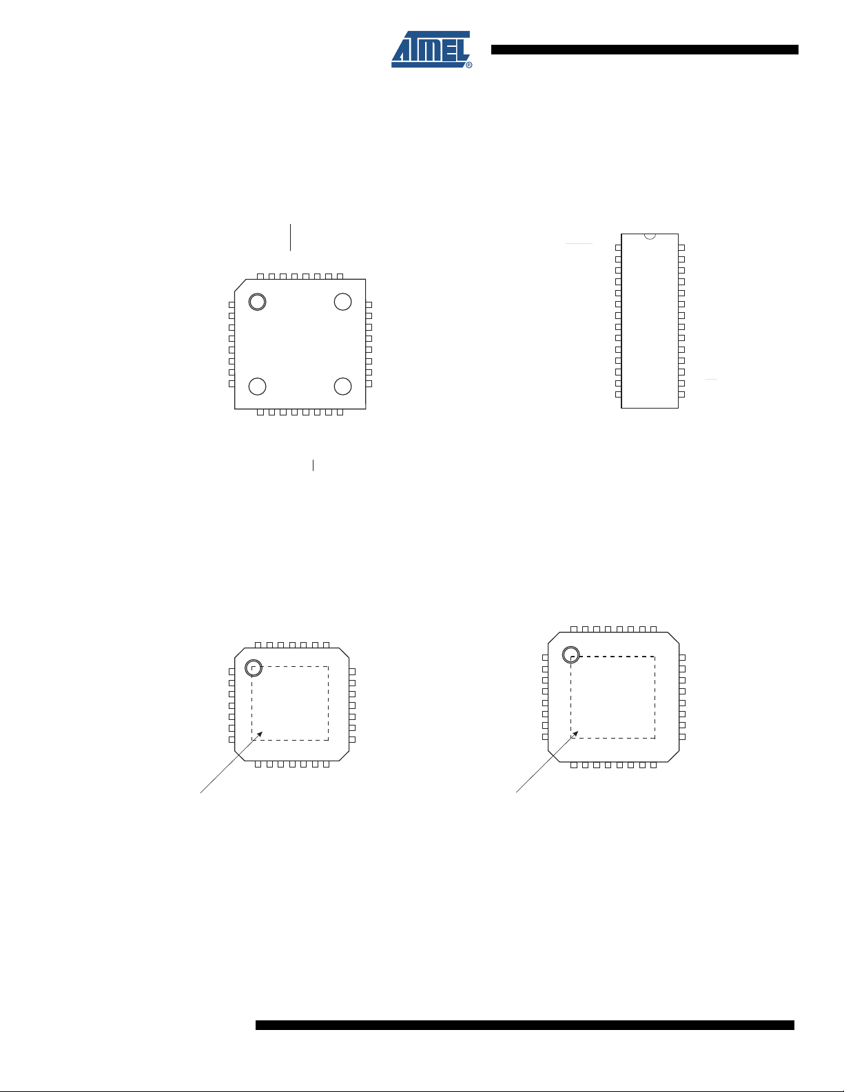
1. Pin Configurations
TQFP Top View
3)
2)
(
Figure 1-1. Pinout of ATtiny48/88
PDIP
(PCINT19/INT1) PD3
(PCINT20/T0) PD4
(PCINT26) PA2
VCC
GND
(PCINT27) PA3
(PCINT6/CLKI) PB6
(PCINT7) PB7
(PCINT19/INT1) PD3
(PCINT20/T0) PD4
(PCINT6/CLKI) PB6
(PCINT21/T1) PD5
VCC
GND
(PCINT7) PB7
PD2 (INT0/PCINT18)
PD1 (PCINT17)
PD0 (PCINT16)
PC6 (RESET/PCINT14)
32313029282726
1
2
3
4
5
6
7
8
9101112131415
(PCINT21/T1) PD5
(PCINT22/AIN0) PD6
(PCINT23/AIN1) PD7
(PCINT0/CLKO/ICP1) PB0
28 MLF Top View
PD2 (INT0/PCINT18)
PD1 (PCINT17)
PD0 (PCINT16)
PC6 (RESET/PCINT14)
PC5 (ADC5/SCL/PCINT13)
28272625242322
1
2
3
4
5
6
7
891011121314
PC5 (ADC5/SCL/PCINT13)
PC4 (ADC4/SDA/PCINT12)
PC3 (ADC3/PCINT11)
PC2 (ADC2/PCINT10)
25
24
PC1 (ADC1/PCINT9)
23
PC0 (ADC0/PCINT8)
22
PA1 (ADC7/PCINT25)
21
GND
20
PC7 (PCINT15)
19
PA0 (ADC6/PCINT24)
18
AVCC
17
PB5 (SCK/PCINT5)
16
(PCINT3/MOSI) PB3
(PCINT4/MISO) PB4
(PCINT1/OC1A) PB1
(PCINT2/SS/OC1B) PB2
PC4 (ADC4/SDA/PCINT12)
PC3 (ADC3/PCINT11)
PC2 (ADC2/PCINT10)
21
PC1 (ADC1/PCINT9)
20
PC0 (ADC0/PCINT8)
19
GND
18
PC7 (PCI NT15)
17
AVCC
16
PB5 (SCK/PCINT5)
15
(PCINT0/CLKO/ICP1) PB0
(PCINT19/INT1) PD3
(PCINT20/T0) PD4
(PCINT26) PA2
VCC
GND
(PCINT27) PA3
(PCINT6/CLKI) PB6
(PCINT7) PB7
(PCINT14/RESET) PC6
(PCINT16) PD0
(PCINT17) PD1
(PCINT18/INT0) PD2
(PCINT19/INT1) PD3
(PCINT20/T0) PD4
(PCINT6/CLKI) PB6
(PCINT21/T1) PD5
(PCINT22/AIN0) PD6
(PCINT23/AIN1) PD7
VCC
GND
(PCINT7) PB7
32 MLF Top View
PD2 (INT0/PCINT18)
PD1 (PCINT17)
PD0 (PCINT16)
32313029282726
1
2
3
4
5
6
7
8
9101112131415
1
2
3
4
5
6
7
8
9
10
11
12
13
14
PC6 (RESET/PCINT14)
PC5 (ADC5/SCL/PCINT13)
28
27
26
25
24
23
22
21
20
19
18
17
16
15
PC4 (ADC4/SDA/PCINT12)
PC3 (ADC3/PCINT11)
PC2 (ADC2/PCINT10)
25
24
23
22
21
20
19
18
17
16
PC5 (ADC5/SCL/PCINT1
PC4 (ADC4/SDA/PCINT1
PC3 (ADC3/PCINT11)
PC2 (ADC2/PCINT10)
PC1 (ADC1/PCINT9)
PC0 (ADC0/PCINT8)
GND
PC7 (PCINT15)
AVCC
PB5 (SCK/PCINT5)
PB4 (MISO/PCINT4)
PB3 (MOSI/PCINT3)
PB2 (SS/OC1B/PCINT2)
PB1 (OC1A/PCINT1)
PC1 (ADC1/PCINT9)
PC0 (ADC0/PCINT8)
PA1 (ADC7/PCINT25)
GND
PC7 (PCINT15)
PA0 (ADC6/PCINT24)
AVCC
PB5 (SCK/PCINT5)
NOTE: Bottom pad should be soldered to ground.
2
(PCINT1/OC1A) PB1
(PCINT22/AIN0) PD6
(PCINT23/AIN1) PD7
(PCINT3//MOSI) PB3
(PCINT2/SS/OC1B) PB2
PCINT0/CLKO/ICP1) PB0
(PCINT4/MISO) PB4
NOTE: Bottom pad should be soldered to ground.
(PCINT21/T1) PD5
(PCINT1/OC1A) PB1
(PCINT22/AIN0) PD6
(PCINT23/AIN1) PD7
PCINT0/CLKO/ICP1) PB0
(PCINT3/MOSI) PB3
(PCINT4/MISO) PB4
(PCINT2/SS/OC1B) PB2
8008AS–AVR–06/08

1.1 Pin Descriptions
1.1.1 VCC
Digital supply voltage.
1.1.2 GND
Ground.
1.1.3 Port A (PA3:0) (in 32-lead TQFP and 32-pad QFN/MLF packages, only)
Port A is a 4-bit bi-directional I/O port with internal pull-up resistors (selected for each bit) in 32lead TQFP and 32-pad QFN/MLF package. The PA3..0 output buffers have symmetrical drive
characteristics with both high sink and source capability. As inputs, Port A pins that are externally pulled low will source current if the pull-up resistors are activated. The Po rt A pins are tristated when a reset condition becomes active, even if the clock is not runn ing.
1.1.4 Port B (PB7:0)
Port B is an 8-bit bi-directional I/O port with internal pull-up resistors (selected for each bit). The
Port B output buffers have symmetrical drive characteristics with both high sink and source
capability. As inputs, Port B pins that are externally pulled low will source current if the pull-up
resistors are activated. The Port B pins are tri-stated when a reset co ndition becomes active,
even if the clock is not running.
ATtiny48/88
Depending on the clock selection fuse settings, PB6 can be used as input to the internal clock
operating circuit.
The various special features of Port B are elaborated in “Alternate Functions of Port B” on page
64 and “System Clock and Clock Options” on page 25.
1.1.5 Port C (PC7, PC5:0)
Port C is a 8-bit bi-directional I/O port with internal pull-up resistors (selected for each bit). The
PC7 and PC5..0 output buffers have symmetrical drive characteristics with both high sink and
source capability. As inputs, Port C pins that are externally pulled low will source current if the
pull-up resistors are activated. The Port C pins are tri-stated when a reset condition becomes
active, even if the clock is not running.
1.1.6 PC6/RESET
If the RSTDISBL Fuse is programmed, PC6 is used as an I/O pin. Note that the electrical characteristics of PC6 differ from those of the other pins of Port C.
If the RSTDISBL Fuse is unprogrammed, PC6 is used as a r eset input . A low level on this pin f or
longer than the minimum pulse width will generate a reset, even if the clock is not running. The
minimum pulse length is given in Table 22-3 on page 201. Shorter pulses are not guaranteed to
generate a reset.
The various special features of Port C are elaborated in “Alternate Functions of Port C” on page
67.
1.1.7 Port D (PD7:0)
8008AS–AVR–06/08
Port D is an 8-bit bi-directional I/O port with internal pull-up resistors (selected for each bit). The
PD7..4 output buffers have symmetrical drive characteristics with both high sink and source
capabilities, while the PD3..0 output buffers hav e stronger sink capabilities. As inp uts, Port D
3

ATtiny48/88
pins that are externally pulled low will source current if the pull-up resistors are activated. The
Port D pins are tri-stated when a reset condition becom es active, even if the clock is not running.
The various special features of Port D are elaborated in “Alternate Functions of Port D” on page
70.
1.1.8 AV
CC
AVCC is the supply voltage pin for the A/D converter and a selection of I/O pins. This pin should
be externally connec ted to V
mended this pin is connected to V
even if the ADC is not used. If the ADC is used, it is recom-
CC
through a low-pass filter, as described in “Analog Noise
CC
Canceling Techniques” on page 163.
The following pins receive their supply voltage from AV
ages) PA1:0. All other I/O pins take their supply voltage from V
: PC7, PC5:0 and (in 32-lead pack-
CC
.
CC
4
8008AS–AVR–06/08
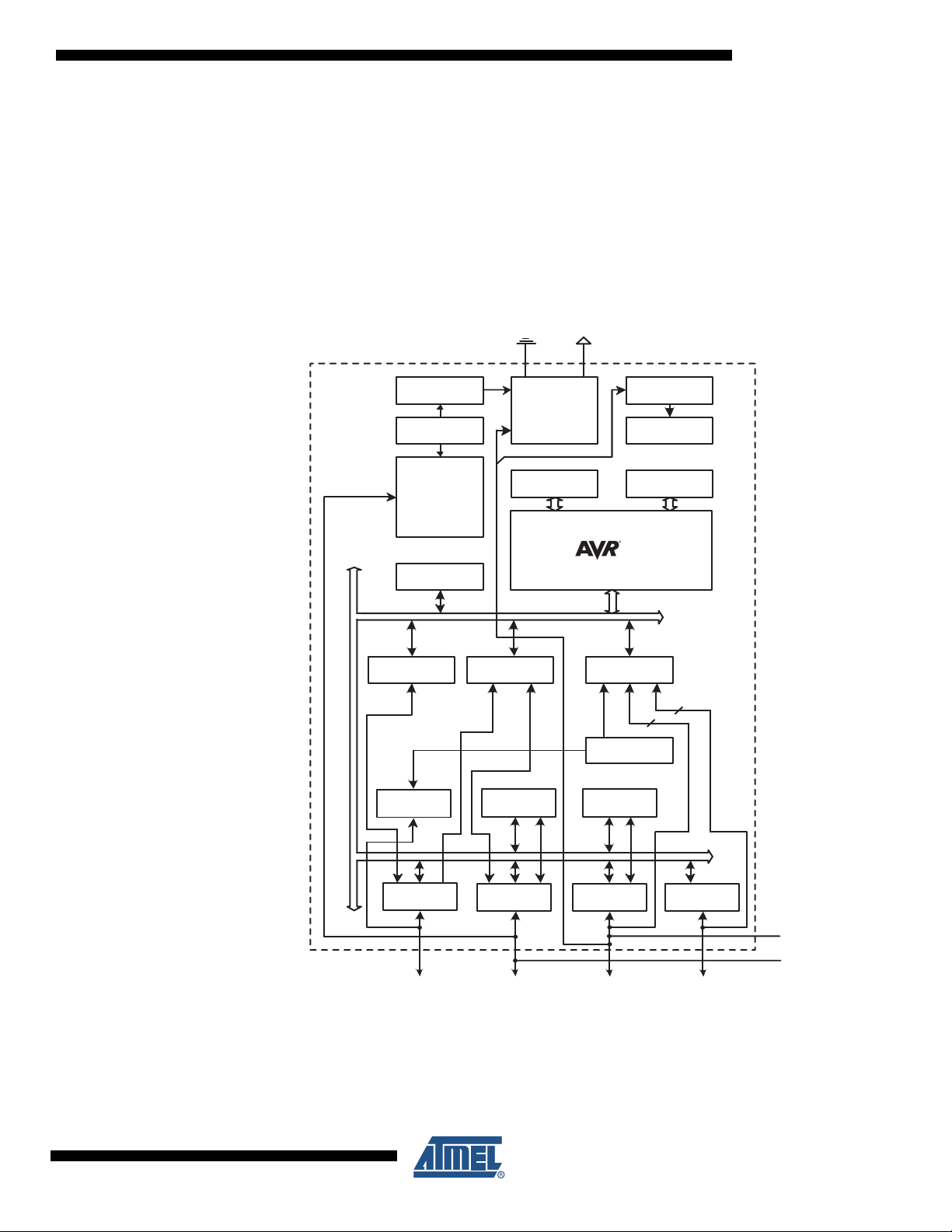
2. Overview
2.1 Block Diagram
ATtiny48/88
The ATtiny48/88 is a low-power CMOS 8-bit microcontroller based on the AVR enhanced RISC
architecture. By executing powerful instructions in a single clock cycle, the ATt iny48/88 achieves
throughputs approaching 1 MIPS pe r MHz allow ing the sy stem de signer to optimize power c onsumption versus processing speed.
Figure 2-1. Block Diagram
GND
Watchdog
Timer
Watchdog
Oscillator
Oscillator
Circuits /
Clock
Generation
EEPROM
16bit T/C 18bit T/C 0 A/D Conv.
DATABUS
Powe r
Supervision
POR / BOD &
RESET
VCC
debugWIRE
CPU
Internal
Bandgap
Program
Logic
SRAMFlash
6
2
8008AS–AVR–06/08
Analog
Comp.
SPI TWI
PORT C (8)PORT B (8)PORT D (8)
PORT A (4)
RESET
CLKI
PA[0..3] (in TQFP and MLF)PC[0..7]PB[0..7]PD[0..7]
The AVR core combines a rich instruction set with 32 general purpose working registers. All the
32 registers are directly connected to the Arithmetic Logic Unit (ALU), allowing two independent
registers to be accessed in one single instruction executed in one clock cycle. The resulting
architecture is more code efficient while achieving throughputs up to ten times faster than conventional CISC microcontrollers.
5
ATtiny48/88
The ATtiny48/88 provides the following features: 4/8K bytes of In-System Programmable Flash,
64/64 bytes EEPROM, 256/512 bytes SRAM, 24 general purpose I/O lines (28 I/Os in 32-lead
TQFP and 32-pad QFN/MLF packages), 32 general purpose working registers, two flexible
Timer/Counters with compare modes, internal and external interrupts, a byte-oriented 2-wire
serial interface, an SPI serial port, a 6-channel 10-bit ADC (8 channels in 32-lead TQFP and 32pad QFN/MLF packages), a programmable Watchdog Timer with internal oscillator, and three
software selectable power saving modes. Idle mode stops the CPU while allowing
Timer/Counters, 2-wire serial interface, SPI port, and interrupt system to continue functioning.
Power-down mode saves the register contents but freezes the oscillator, disabling all other chip
functions until the next interrupt or hardware reset. ADC Noise Reduction mode stops the CPU
and all I/O modules except ADC, and helps to minimize switching noise during ADC
conversions.
The device is manufactured using Atmel’s high density non-volatile memory technology. The
On-chip ISP Flash allows the program memory to be reprogrammed In-System through an SPI
serial interface, by a conventional non-volatile memory programmer, or by an On-chip Boot program running on the AVR core. The Boot program can use any interface to download the
application program in the Flash memory. By combining an 8-bit RISC CPU with In-System SelfProgrammable Flash on a monolithic chip, the Atmel ATtiny48/88 is a powerful microcontroller
that provides a highly flexible and cost effective solutio n to many embedded contro l applications.
The ATtiny48/88 AVR is supported by a full suite of program and system development tools
including: C compilers, macro assemblers, program debugger/simulators and evaluation kits.
2.2 Comparison Between ATtiny48 and ATtiny88
The ATtiny48 and ATtiny88 differ only in memory sizes. Table 2-1 summarizes the different
memory sizes for the two devices.
Table 2-1. Memory Size Summary
Device Flash EEPROM RAM
ATtiny48 4K Bytes 64 Bytes 256 Bytes
ATtiny88 8K Bytes 64 Bytes 512 Bytes
6
8008AS–AVR–06/08

3. About
3.1 Resources
A comprehensive set of development tools, application notes and datasheets are available for
download at http://www.atmel.com/avr.
3.2 About Code Examples
This documentation contains simple code examples t hat brief ly show h ow to us e various parts of
the device. These code examples assume that the part specific header file is included b efore
compilation. Be aware that not all C compiler vendors include bit definitions in the header files
and interrupt handling in C is compiler dependent . Please con firm wit h the C com piler d ocume ntation for more details.
For I/O Registers located in extended I/O map, “IN”, “OUT”, “SBIS”, “SBIC”, “CBI”, and “SBI”
instructions must be replaced with instructions that allow access to extended I/O. Typically
“LDS” and “STS” combined with “SBRS”, “SBRC”, “SBR”, and “CBR”.
3.3 Data Retention
Reliability Qualification results show that the projected data retention failure rate is much less
than 1 PPM over 20 years at 85°C or 100 years at 25°C.
ATtiny48/88
3.4 Disclaimer
Typical values contained in this datasheet are based on simulations and characterization of
other AVR microcontrollers manufactured o n th e same proce ss te ch nolo gy. Min a nd Ma x valu es
will be available after the device is characterized.
8008AS–AVR–06/08
7

ATtiny48/88
4. Register Summary
Address Name Bit 7 Bit 6 Bit 5 Bit 4 Bit 3 Bit 2 Bit 1 Bit 0 Page
(0xFF) Reserved – – – – – – – –
(0xFE) Reserved – – – – – – – –
(0xFD) Reserved – – – – – – – –
(0xFC) Reserved
(0xFB) Reserved
(0xFA) Reserved – – – – – – – –
(0xF9) Reserved – – – – – – – –
(0xF8) Reserved – – – – – – – –
(0xF7) Reserved – – – – – – – –
(0xF6) Reserved – – – – – – – –
(0xF5) Reserved – – – – – – – –
(0xF4) Reserved – – – – – – – –
(0xF3) Reserved – – – – – – – –
(0xF2) Reserved – – – – – – – –
(0xF1) Reserved – – – – – – – –
(0xF0) Reserved
(0xEF) Reserved
(0xEE) Reserved – – – – – – – –
(0xED) Reserved – – – – – – – –
(0xEC) Reserved – – – – – – – –
(0xEB) Reserved – – – – – – – –
(0xEA) Reserved – – – – – – – –
(0xE9) Reserved – – – – – – – –
(0xE8) Reserved – – – – – – – –
(0xE7) Reserved – – – – – – – –
(0xE6) Reserved – – – – – – – –
(0xE5) Reserved – – – – – – – –
(0xE4) Reserved – – – – – – – –
(0xE3) Reserved – – – – – – – –
(0xE2) Reserved – – – – – – – –
(0xE1) Reserved – – – – – – – –
(0xE0) Reserved – – – – – – – –
(0xDF) Reserved – – – – – – – –
(0xDE) Reserved – – – – – – – –
(0xDD) Reserved – – – – – – – –
(0xDC) Reserved – – – – – – – –
(0xDB) Reserved – – – – – – – –
(0xDA) Reserved – – – – – – – –
(0xD9) Reserved – – – – – – – –
(0xD8) Reserved – – – – – – – –
(0xD7) Reserved – – – – – – – –
(0xD6) Reserved – – – – – – – –
(0xD5) Reserved
(0xD4) Reserved
(0xD3) Reserved – – – – – – – –
(0xD2) Reserved
(0xD1) Reserved
(0xD0) Reserved
(0xCF) Reserved – – – – – – – –
(0xCE) Reserved
(0xCD) Reserved
(0xCC) Reserved – – – – – – – –
(0xCB) Reserved
(0xCA) Reserved
(0xC9) Reserved – – – – – – – –
(0xC8) Reserved
(0xC7) Reserved
(0xC6) Reserved – – – – – – – –
(0xC5) Reserved
(0xC4) Reserved – – – – – – – –
(0xC3) Reserved
(0xC2) Reserved
(0xC1) Reserved – – – – – – – –
(0xC0) Reserved – – – – – – – –
– – – – – – – –
– – – – – – – –
– – – – – – – –
– – – – – – – –
– – – – – – – –
– – – – – – – –
– – – – – – – –
– – – – – – – –
– – – – – – – –
– – – – – – – –
– – – – – – – –
– – – – – – – –
– – – – – – – –
– – – – – – – –
– – – – – – – –
– – – – – – – –
– – – – – – – –
– – – – – – – –
8
8008AS–AVR–06/08

ATtiny48/88
Address Name Bit 7 Bit 6 Bit 5 Bit 4 Bit 3 Bit 2 Bit 1 Bit 0 Page
(0xBF) Reserved – – – – – – – –
(0xBE) TWHSR – – – – – – –TWHS 152
(0xBD) TWAMR TWAM6 TWAM5 TWAM4 TWAM3 TWAM2 TWAM1 TWAM0 –152
(0xBC) TWCR TWINT TWEA TWSTA TWSTO TWWC TWEN –TWIE 149
(0xBB) TWDR 2-wire Serial Interface Data Register 151
(0xBA) TWAR TWA6 TWA5 TWA4 TWA3 TWA2 TWA1 TWA0 TWGCE 151
(0xB9) TWSR TWS7 TWS6 TWS5 TWS4 TWS3 –TWPS1TWPS0 150
(0xB8) TWBR 2-wire Serial Interface Bit Rate Register 149
(0xB7) Reserved – – – – – – – –
(0xB6) Reserved – – – – – – – –
(0xB5) Reserved – – – – – – – –
(0xB4) Reserved – – – – – – – –
(0xB3) Reserved – – – – – – – –
(0xB2) Reserved – – – – – – – –
(0xB1) Reserved – – – – – – – –
(0xB0) Reserved – – – – – – – –
(0xAF) Reserved
(0xAE) Reserved
(0xAD) Reserved – – – – – – – –
(0xAC) Reserved
(0xAB) Reserved
(0xAA) Reserved – – – – – – – –
(0xA9) Reserved – – – – – – – –
(0xA8) Reserved – – – – – – – –
(0xA7) Reserved – – – – – – – –
(0xA6) Reserved – – – – – – – –
(0xA5) Reserved – – – – – – – –
(0xA4) Reserved – – – – – – – –
(0xA3) Reserved – – – – – – – –
(0xA2) Reserved – – – – – – – –
(0xA1) Reserved – – – – – – – –
(0xA0) Reserved – – – – – – – –
(0x9F) Reserved – – – – – – – –
(0x9E) Reserved – – – – – – – –
(0x9D) Reserved – – – – – – – –
(0x9C) Reserved – – – – – – – –
(0x9B) Reserved – – – – – – – –
(0x9A) Reserved – – – – – – – –
(0x99) Reserved – – – – – – – –
(0x98) Reserved – – – – – – – –
(0x97) Reserved – – – – – – – –
(0x96) Reserved – – – – – – – –
(0x95) Reserved – – – – – – – –
(0x94) Reserved
(0x93) Reserved
(0x92) Reserved – – – – – – – –
(0x91) Reserved
(0x90) Reserved
(0x8F) Reserved
(0x8E) Reserved – – – – – – – –
(0x8D) Reserved
(0x8C) Reserved
(0x8B) OCR1BH Timer/Counter1 – Output Compare Register B High Byte 108
(0x8A) OCR1BL Timer/Counter1
(0x89) OCR1AH Timer/Counter1
(0x88) OCR1AL Timer/Counter1 – Output Compare Register A Low Byte 108
(0x87) ICR1H Timer/Counter1
(0x86) ICR1L Timer/Counter1
(0x85) TCNT1H Timer/Counter1 – Counter Register High Byte 108
(0x84) TCNT1L Timer/Counter1
(0x83) Reserved – – – – – – – –
(0x82) TCCR1C FOC1A FOC1B
(0x81) TCCR1B ICNC1 ICES1
(0x80) TCCR1A COM1A1 COM1A0 COM1B1 COM1B0 – –WGM11WGM10 104
(0x7F) DIDR1
(0x7E) DIDR0 ADC7D ADC6D ADC5D ADC4D ADC3D ADC2D ADC1D ADC0D 171
– – – – – – – –
– – – – – – – –
– – – – – – – –
– – – – – – – –
– – – – – – – –
– – – – – – – –
– – – – – – – –
– – – – – – – –
– – – – – – – –
– – – – – – – –
– – – – – – – –
– Output Compare Register B Low Byte 108
– Output Compare Register A High Byte 108
– Input Capture Register High Byte 109
– Input Capture Register Low Byte 109
– Counter Register Low Byte 108
– – – – – –107
– WGM13 WGM12 CS12 CS11 CS10 106
– – – – –
–
AIN1D AIN0D 155
8008AS–AVR–06/08
9

ATtiny48/88
Address Name Bit 7 Bit 6 Bit 5 Bit 4 Bit 3 Bit 2 Bit 1 Bit 0 Page
(0x7D) Reserved – – – – – – – –
(0x7C) ADMUX – REFS0 ADLAR – MUX3 MUX2 MUX1 MUX0 167
(0x7B) ADCSRB –ACME– – – ADTS2 ADTS1 ADTS0 170
(0x7A) ADCSRA ADEN ADSC ADATE ADIF ADIE ADPS2 ADPS1 ADPS0 168
(0x79) ADCH ADC Data Register High byte 169
(0x78) ADCL ADC Data Register Low byte 169
(0x77) Reserved – – – – – – – –
(0x76) Reserved – – – – – – – –
(0x75) Reserved – – – – – – – –
(0x74) Reserved – – – – – – – –
(0x73) Reserved – – – – – – – –
(0x72) Reserved – – – – – – – –
(0x71) Reserved – – – – – – – –
(0x70) Reserved – – – – – – – –
(0x6F) TIMSK1 – –ICIE1 – – OCIE1B OCIE1A TOIE1 109
(0x6E) TIMSK0 – – – – – OCIE0B OCIE0A TOIE0 82
(0x6D) PCMSK2 PCINT23 PCINT22 PCINT21 PCINT20 PCINT19 PCINT18 PCINT17 PCINT16 54
(0x6C) PCMSK1 PCINT15 PCINT14 PCINT13 PCINT12 PCINT11 PCINT10 PCINT9 PCINT8 54
(0x6B) PCMSK0 PCINT7 PCINT6 PCINT5 PCINT4 PCINT3 PCINT2 PCINT1 PCINT0 54
(0x6A) PCMSK3
(0x69) EICRA
(0x68) PCICR – – – – PCIE3 PCIE2 PCIE1 PCIE0 52
(0x67) Reserved – – – – – – – –
(0x66) OSCCAL Oscillator Calibration Regi ster 30
(0x65) Reserved – – – – – – – –
(0x64) PRR PRTWI –PRTIM0 – PRTIM1 PRSPI –PRADC 35
(0x63) Reserved – – – – – – – –
(0x62) Reserved – – – – – – – –
(0x61) CLKPR CLKPCE – – – CLKPS3 CLKPS2 CLKPS1 CLKPS0 31
(0x60) WDTCSR WDIF WDIE WDP3 WDCE WDE WDP2 WDP1 WDP0 44
0x3F (0x5F) SREG I T H S V N Z C 9
0x3E (0x5E) Reserved – – – – – – – –
0x3D (0x5D) SPL SP7 SP6 SP5 SP4 SP3 SP2 SP1 SP0 12
0x3C (0x5C) Reserved – – – – – – – –
0x3B (0x5B) Reserved – – – – – – – –
0x3A (0x5A) Reserved – – – – – – – –
0x39 (0x59) Reserved – – – – – – – –
0x38 (0x58) Reserved – – – – – – – –
0x37 (0x57) SPMCSR – – – CTPB RFLB PGWRT PGERS SELFPRGEN 179
0x36 (0x56) Reserved – – – – –
0x35 (0x55) MCUCR – BPDS BPDSE PUD – – – –
0x34 (0x54) MCUSR – – – – WDRF BORF EXTRF PORF 44
0x33 (0x53) SMCR – – – – –SM1SM0SE 36
0x32 (0x52) Reserved
0x31 (0x51) DWDR
0x30 (0x50) ACSR ACD ACBG ACO ACI ACIE ACIC ACIS1 ACIS0 154
0x2F (0x4F) Reserved – – – – – – – –
0x2E (0x4E) SPDR SPI Data Register 122
0x2D (0x4D) SPSR SPIF WCOL – – – – – SPI2X 121
0x2C (0x4C) SPCR SPIE SPE DORD MSTR CPOL CPHA SPR1 SPR0 120
0x2B (0x4B) GPIOR2 General Purpose I/O Register 2 24
0x2A (0x4A) GPIOR1 General Purpose I/O Register 1 24
0x29 (0x49) Reserved – – – – – – – –
0x28 (0x48) OCR0B Timer/Counter0 Output Compare Register B 82
0x27 (0x47) OCR0A Timer/Counter0 Output Compare Register A 81
0x26 (0x46) TCNT0 Timer/Counter0 (8-bit) 81
0x25 (0x45) TCCR0A
0x24 (0x44) Reserved
0x23 (0x43) GTCCR TSM – – – – – – PSRSYNC 112
0x22 (0x42) Reserved
0x21 (0x41) EEARL EEPROM Address Register Low Byte 22
0x20 (0x40) EEDR EEPROM Data Register 22
0x1F (0x3F) EECR – – EEPM1 EEPM0 EERIE EEMPE EEPE EERE 22
0x1E (0x3E) GPIOR0 General Purpose I/O Register 0 24
0x1D (0x3D) EIMSK
0x1C (0x3C) EIFR – – – – – – INTF1 INTF0 52
– – - – – – –ISC11ISC10ISC01ISC00 50
– – – – – – – –
debugWire Data Register
– – – – CTC0 CS02 CS01 CS00 80
– – – – – – – –
– – – – – – – –
– – – – – –INT1INT0 51
PCINT27
PCINT26
PCINT25 PCINT24
54
173
10
8008AS–AVR–06/08

ATtiny48/88
Address Name Bit 7 Bit 6 Bit 5 Bit 4 Bit 3 Bit 2 Bit 1 Bit 0 Page
0x1B (0x3B) PCIFR – – – – PCIF3 PCIF2 PCIF1 PCIF0 53
0x1A (0x3A) Reserved – – – – – – – –
0x19 (0x39) Reserved – – – – – – – –
0x18 (0x38) Reserved – – – – – – – –
0x17 (0x37) Reserved – – – – – – – –
0x16 (0x36) TIFR1 – –ICF1 – – OCF1B OCF1A TOV1 110
0x15 (0x35) TIFR0 – – – – – OCF0B OCF0A TOV0 82
0x14 (0x34) Reserved – – – – – – – –
0x13 (0x33) Reserved – – – – – – – –
0x12 (0x32) PORTCR BBMD BBMC BBMB BBMA PUDD PUDC PUDB PUDA 72
0x11 (0x31) Reserved – – – – – – – –
0x10 (0x30) Reserved – – – – – – – –
0x0F (0x2F) Reserved – – – – – – – –
0x0E (0x2E) PORTA – – – – PORTA3 PORTA2 PORTA1 PORTA0 74
0x0D (0x2D) DDRA – – – – DDA3 DDA2 DDA1 DDA0 74
0x0C (0x2C) PINA – – – – PINA3 PINA2 PINA1 PINA0
0x0B (0x2B) PORTD PORTD7 PORTD6 PORTD5 PORTD4 PORTD3 PORTD2 PORTD1 PORTD0 74
0x0A (0x2A) DDRD DDD7 DDD6 DDD5 DDD4 DDD3 DDD2 DDD1 DDD0 74
0x09 (0x29) PIND PIND7 PIND6 PIND5 PIND4 PIND3 PIND2 PIND1 PIND0 74
0x08 (0x28) PORTC PORTC7 PORTC6 PORTC5 PORTC4 PORTC3 PORTC2 PORTC1 PORTC0 73
0x07 (0x27) DDRC DDC7 DDC6 DDC5 DDC4 DDC3 DDC2 DDC1 DDC0 73
0x06 (0x26) PINC PINC7 PINC6 PINC5 PINC4 PINC3 PINC2 PINC1 PINC0 74
0x05 (0x25) PORTB PORTB7 PORTB6 PORTB5 PORTB4 PORTB3 PORTB2 PORTB1 PORTB0 73
0x04 (0x24) DDRB DDB7 DDB6 DDB5 DDB4 DDB3 DDB2 DDB1 DDB0 73
0x03 (0x23) PINB PINB7 PINB6 PINB5 PINB4 PINB3 PINB2 PINB1 PINB0 73
0x02 (0x22) Reserved – – – – – – – –
0x01 (0x21) Reserved – – – – – – – –
0x00 (0x20) Reserved – – – – – – – –
Note: 1. For compatibility with future devices, reserved bits should be written to zero if accessed. Reserved I/O memory addresses
should never be written.
2. I/O Registers within the address range 0x00 – 0x1F are directly bit-accessible using the SBI and CBI instructions. In these
registers, the value of single bits can be checked by using the SBIS and SBIC instructions.
3. Some of the Status Flags are cleared by writing a logical one to them. Note that, unlike most other AVRs, the CBI and SBI
instructions will only operate on the specified bit, and can therefore be used on registers containing such Status Flags. The
CBI and SBI instructions work with registers 0x00 to 0x1F only.
4. When using the I/O specific commands IN and OUT, the I/O addresses 0x00 – 0x3F must be used. When addressing I/O
Registers as data space using LD and ST instructions, 0x20 must be added to these addresses. The ATtiny48/88 is a complex microcontroller with more peripheral units than can be supported within the 64 location reserved in Opcode for the IN
and OUT instructions. For the Extended I/O space from 0x60
– 0xFF in SRAM, only the ST/STS/STD and LD/LDS/LDD
instructions can be used.
74
8008AS–AVR–06/08
11

ATtiny48/88
5. Instruction Set Summary
Mnemonics Operands Description Operation Flags #Clocks
ARITHMETIC AND LOGIC INSTRUCTIONS
ADD Rd, Rr Add two Registers Rd ← Rd + Rr Z,C,N,V,H 1
ADC Rd, Rr Add with Carry two Registers Rd ← Rd + Rr + C Z,C,N,V,H 1
ADIW Rdl,K Add Immediate to Word Rdh:Rdl ← Rdh:Rdl + K Z,C,N,V,S 2
SUB Rd, Rr Subtract two Registers Rd ← Rd - Rr Z,C,N,V,H 1
SUBI Rd, K Subtract Constant from Register Rd ← Rd - K Z,C,N,V,H 1
SBC Rd, Rr Subtract with Carry two Registers Rd ← Rd - Rr - C Z,C,N,V,H 1
SBCI Rd, K Subtract with Carry Constant from Reg. Rd ← Rd - K - C Z,C,N,V,H 1
SBIW Rdl,K Subtract Immediate fro m Word Rdh:Rdl ← Rdh:Rdl - K Z,C,N,V,S 2
AND Rd, Rr Logical AND Registers Rd ← Rd • Rr Z,N,V 1
ANDI Rd, K Logical AND Register and Constant Rd ← Rd • K Z,N,V 1
OR Rd, Rr Logical OR Registers Rd ← Rd v Rr Z,N,V 1
ORI Rd, K Logical OR Register and Constant Rd ← Rd v K Z,N,V 1
EOR Rd, Rr Exclusive OR Registers Rd ← Rd ⊕ Rr Z,N,V 1
COM Rd One’s Complement Rd ← 0xFF − Rd Z,C,N,V 1
NEG Rd Two’s Complement Rd ← 0x00 − Rd Z,C,N,V,H 1
SBR Rd,K Set Bit(s) in Register Rd ← Rd v K Z,N,V 1
CBR Rd,K Clear Bit(s) in Register Rd ← Rd • (0xFF - K) Z,N,V 1
INC Rd Increment Rd ← Rd + 1 Z,N,V 1
DEC Rd Decrement Rd ← Rd − 1 Z,N,V 1
TST Rd Test for Zero or Minus Rd ← Rd • Rd Z,N,V 1
CLR Rd Clear Register Rd ← Rd ⊕ Rd Z,N,V 1
SER Rd Set Register Rd ← 0xFF None 1
BRANCH INSTRUCTIONS
RJMP k Relative Jump PC ← PC + k + 1 None 2
IJMP Indirect Jump to (Z) PC ← Z None 2
RCALL k Relative Subroutine Call PC ← PC + k + 1 None 3
ICALL Indirect Call to (Z) PC ← ZNone3
RET Subroutine Return PC ← STACK None 4
RETI Interrupt Return PC ← STACK I 4
CPSE Rd,Rr Compare, Skip if Equal if (Rd = Rr) PC ← PC + 2 or 3 None 1/2/3
CP Rd,Rr Compare Rd − Rr Z, N,V,C,H 1
CPC Rd,Rr Compare with Carry Rd − Rr − C Z, N,V,C,H 1
CPI Rd,K Compare Register with Immediate Rd − K Z, N,V,C,H 1
SBRC Rr, b Skip if Bit in Register Cleared if (Rr(b)=0) PC ← PC + 2 or 3 None 1/2/3
SBRS Rr, b Skip if Bit in Register is Set if (Rr(b)=1) PC ← PC + 2 or 3 None 1/2/3
SBIC P, b Skip if Bit in I/O Register Cleared if (P(b)=0) PC ← PC + 2 or 3 None 1/2/3
SBIS P, b Skip if Bit in I/O Register is Set if (P(b)=1) PC ← PC + 2 or 3 None 1/2/3
BRBS s, k Branch if Status Flag Set if (SREG(s) = 1) then PC←PC+k + 1 None 1/2
BRBC s, k Branch if Status Flag Cleared if (SREG(s) = 0) then PC←PC+k + 1 None 1/2
BREQ k Branch if Equal if (Z = 1) then PC ← PC + k + 1 None 1/2
BRNE k Branch if Not Equal if (Z = 0) then PC ← PC + k + 1 None 1/2
BRCS k Branch if Carry Set if (C = 1) then PC ← PC + k + 1 None 1/2
BRCC k Branch if Carry Cleared if (C = 0) then PC ← PC + k + 1 None 1/2
BRSH k Branch if Same or Higher if (C = 0) then PC ← PC + k + 1 None 1/2
BRLO k Branch if Lower if (C = 1) then PC ← PC + k + 1 None 1/2
BRMI k Branch if Minus if (N = 1) then PC ← PC + k + 1 None 1/2
BRPL k Branch if Plus if (N = 0) then PC ← PC + k + 1 None 1/2
BRGE k Branch if Greater or Equal, Signed if (N ⊕ V= 0) then PC ← PC + k + 1 None 1/2
BRLT k Branch if Less Than Zero, Signed if (N ⊕ V= 1) then PC ← PC + k + 1 None 1/2
BRHS k Branch if Half Carry Flag Set if (H = 1) then PC ← PC + k + 1 None 1/2
BRHC k Branch if Half Carry Flag Cleared if (H = 0) then PC ← PC + k + 1 None 1/2
BRTS k Branch if T Flag Set if (T = 1) then PC ← PC + k + 1 None 1/2
BRTC k Branch if T Flag Cleared if (T = 0) then PC ← PC + k + 1 None 1/2
BRVS k Branch if Overflow Flag is Set if (V = 1) then PC ← PC + k + 1 None 1/2
BRVC k Branch if Overflow Flag is Cleared if (V = 0) then PC ← PC + k + 1 None 1/2
BRIE k Branch if Interrupt Enabled if ( I = 1) then PC ← PC + k + 1 None 1/2
BRID k Branch if Interrupt Disabled if ( I = 0) then PC ← PC + k + 1 None 1/2
BIT AND BIT-TEST INSTRUCTIONS
SBI P,b Set Bit in I/O Register I/O(P,b) ← 1None2
CBI P,b Clear Bit in I/O Register I/O(P,b) ← 0None2
LSL Rd Logical Shift Left Rd(n+1) ← Rd(n), Rd(0)
LSR Rd Logical Shift Right Rd(n) ← Rd(n+1), Rd(7) ← 0 Z,C,N,V 1
ROL Rd Rotate Left Through Carry Rd(0)←C,Rd(n+1)← Rd(n),C←Rd(7) Z,C,N,V 1
← 0 Z,C,N,V 1
12
8008AS–AVR–06/08

ATtiny48/88
Mnemonics Operands Description Operation Flags #Clocks
ROR Rd Ro ta te Right Through Carry Rd(7)←C,Rd(n)← Rd(n+1),C←Rd(0) Z,C,N,V 1
ASR Rd Arithmetic Shift Right Rd(n) ← Rd(n+1), n=0..6 Z,C,N,V 1
SWAP Rd Swap Nibbles Rd(3..0)←Rd(7..4),Rd(7..4)←Rd(3..0) None 1
BSET s Flag Set SREG(s) ← 1 SREG(s) 1
BCLR s Flag Clear SREG(s) ← 0 SREG(s) 1
BST Rr, b Bit Store from Register to T T ← Rr(b) T 1
BLD Rd, b Bit load from T to Register Rd(b) ← TNone1
SEC Set Carry C ← 1C1
CLC Clear Carry C ← 0 C 1
SEN Set Negative Flag N ← 1N1
CLN Clear Negative Flag N ← 0 N 1
SEZ Set Zero Flag Z ← 1Z1
CLZ Clear Zero Flag Z ← 0 Z 1
SEI Global Interrupt Enable I ← 1I1
CLI Global Interrupt Disable I ← 0 I 1
SES Set Signed Test Flag S ← 1S1
CLS Clear Signed Test Flag S ← 0 S 1
SEV Set Twos Complement Overflow. V ← 1V1
CLV Clear Twos Complement Overflow V ← 0 V 1
SET Set T in SREG T ← 1T1
CLT Clear T in SREG T ← 0 T 1
SEH Set Half Carry Flag in SREG H ← 1H1
CLH Clear Half Carry Flag in SREG H ← 0 H 1
DATA TRANSFER INSTRUCTIONS
MOV Rd, Rr Move Between Registers Rd ← Rr None 1
MOVW Rd, Rr Copy Register Word
LDI Rd, K Load Immediate Rd ← KNone1
LD Rd, X Load Indirect Rd ← (X) None 2
LD Rd, X+ Load Indirect and Post-Inc. Rd ← (X), X ← X + 1 None 2
LD Rd, - X Load Indirect and Pre-Dec. X ← X - 1, Rd ← (X) None 2
LD Rd, Y Load Indirect Rd ← (Y) None 2
LD Rd, Y+ Load Indirect and Post-Inc. Rd ← (Y), Y ← Y + 1 None 2
LD Rd, - Y Load Indirect and Pre-Dec. Y ← Y - 1, Rd ← (Y) None 2
LDD Rd,Y+q Load Indirect with Displacement Rd ← (Y + q) None 2
LD Rd, Z Load Indirect Rd ← (Z) None 2
LD Rd, Z+ Load Indirect and Post-Inc. Rd ← (Z), Z ← Z+1 None 2
LD Rd, -Z Load Indirect and Pre-Dec. Z ← Z - 1, Rd ← (Z) None 2
LDD Rd, Z+q Load Indirect with Displacement Rd ← (Z + q) None 2
LDS Rd, k Load Direct from SRAM Rd ← (k) None 2
ST X, Rr Store Indirect (X) ← Rr None 2
ST X+, Rr Store Indirect and Post-Inc. (X) ← Rr, X ← X + 1 None 2
ST - X, Rr Store Indirect and Pre-Dec. X ← X - 1, (X) ← Rr None 2
ST Y, Rr Store Indirect (Y ) ← Rr None 2
ST Y+, Rr Store Indirect and Post-Inc. (Y) ← Rr, Y ← Y + 1 None 2
ST - Y, Rr Store Indirect and Pre-Dec. Y ← Y - 1, (Y) ← Rr None 2
STD Y+q,Rr Store Indirect with Displacement (Y + q) ← Rr None 2
ST Z, Rr Store Indirect (Z) ← Rr None 2
ST Z+, Rr Store Indirect and Post-Inc. (Z) ← Rr, Z ← Z + 1 None 2
ST -Z, Rr Store Indirect and Pre-Dec. Z ← Z - 1, (Z) ← Rr None 2
STD Z+q,Rr Store Indirect with Displacement (Z + q) ← Rr None 2
STS k, Rr Store Direct to SRAM (k) ← Rr None 2
LPM Load Pr ogram Memory R0 ← (Z) None 3
LPM Rd, Z Load Program Memory Rd ← (Z) None 3
LPM Rd, Z+ Load Program Memory and Post-Inc Rd ← (Z), Z ← Z+1 None 3
SPM Store Program Memory (Z) ← R1:R0 None IN Rd, P In Port Rd ← PNone1
OUT P, Rr Out Port P ← Rr None 1
PUSH Rr Push Register on Stack STACK ← Rr None 2
POP Rd Pop Register from Stack Rd ← STACK None 2
MCU CONTROL INSTRUCTIONS
NOP No Operation None 1
SLEEP Sleep (see specific descr. for Sleep function) None 1
WDR Watchdog Reset (see specific descr. for WDR/timer) None 1
BREAK Break For On-chip Debug Only None N/A
Rd+1:Rd ← Rr+1:Rr
None 1
8008AS–AVR–06/08
13

ATtiny48/88
6. Ordering Information
6.1 ATtiny48
Speed (MHz) Power Supply Ordering Code Package
ATtiny48-AU
(3)
12
Note: 1. This de vice can also be supplied in wafer f orm. Please contact your local Atmel sales office for detailed ordering information
and minimum quantities.
2. Pb-free packaging alternative, complies to the European Directive for Restriction of Hazardous Substances (RoHS directive).Also Halide free and fully Green.
3. Maximum frequency. See Figure 22-1 on page 200.
1.8 – 5.5
ATtiny48-MMU
ATtiny48-MU
ATtiny48-PU
32A
28M1
32M1-A
28P3
(1)
Operational Range
Industrial
°C to 85°C)
(-40
32A 32-lead, Thin (1.0 mm) Plastic Quad Flat Package (TQFP)
28M1 28-pad, 4 x 4 x 1.0 body, Lead Pitch 0.45 mm Quad Flat No-Lead/Micro Lead Frame Package (QFN/MLF)
32M1-A 32-pad, 5 x 5 x 1.0 body, Lead Pitch 0.50 mm Quad Flat No-Lead/Micro Lead Frame Package (QFN/MLF)
28P3 28-lead, 0.300” Wide, Plastic Dual Inline Package (PDIP)
14
Package Type
8008AS–AVR–06/08

6.2 ATtiny88
ATtiny48/88
Speed (MHz) Power Supply Ordering Code Package
ATtiny88-AU
(3)
12
Note: 1. This de vice can also be supplied in wafer f orm. Please contact your local Atmel sales office for detailed ordering information
and minimum quantities.
2. Pb-free packaging alternative, complies to the European Directive for Restriction of Hazardous Substances (RoHS directive).Also Halide free and fully Green.
3. Maximum frequency. See Figure 22-1 on page 200.
1.8 – 5.5
ATtiny88-MMU
ATtiny88-MU
ATtiny88-PU
32A
28M1
32M1-A
28P3
(1)
Operational Range
Industrial
°C to 85°C)
(-40
Package Type
32A 32-lead, Thin (1.0 mm) Plastic Quad Flat Package (TQFP)
28M1 28-pad, 4 x 4 x 1.0 body, Lead Pitch 0.45 mm Quad Flat No-Lead/Micro Lead Frame Package (QFN/MLF)
32M1-A 32-pad, 5 x 5 x 1.0 body, Lead Pitch 0.50 mm Quad Flat No-Lead/Micro Lead Frame Package (QFN/MLF)
28P3 28-lead, 0.300” Wide, Plastic Dual Inline Package (PDIP)
8008AS–AVR–06/08
15

ATtiny48/88
7. Packaging Information
.
7.1 32A
PIN 1
PIN 1 IDENTIFIER
B
e
E1 E
D1
D
C
0˚~7˚
A1
L
Notes: 1. This package conforms to JEDEC reference MS-026, Variation ABA.
2. Dimensions D1 and E1 do not include mold protrusion. Allowable
protrusion is 0.25 mm per side. Dimensions D1 and E1 are maximum
plastic body size dimensions including mold mismatch.
3. Lead coplanarity is 0.10 mm maximum.
A2 A
SYMBOL
COMMON DIMENSIONS
(Unit of Measure = mm)
MIN
A – – 1.20
A1 0.05 – 0.15
A2 0.95 1.00 1.05
D 8.75 9.00 9.25
D1 6.90 7.00 7.10 Note 2
E 8.75 9.00 9.25
E1 6.90 7.00 7.10 Note 2
B 0.30 – 0.45
C 0.09 – 0.20
L 0.45 – 0.75
e 0.80 TYP
NOM
MAX
NOTE
R
16
2325 Orchard Parkway
San Jose, CA 95131
TITLE
32A, 32-lead, 7 x 7 mm Body Size, 1.0 mm Body Thickness,
0.8 mm Lead Pitch, Thin Profile Plastic Quad Flat Package (TQFP)
10/5/2001
DRAWING NO.
32A
8008AS–AVR–06/08
REV
B

7.2 28M1
1
2
3
D
Pin 1 ID
ATtiny48/88
C
E
SIDE VIEW
TOP VIEW
K
D2
R 0.20
b
BOTTOM VIEW
The terminal #1 ID is a Laser-marked Feature.
Note:
A1
A
y
0.45
1
2
3
E2
L
e
SYMBOL
A 0.80 0.90 1.00
A1 0.00 0.02 0.05
b 0.17 0.22 0.27
C 0.20 REF
D 3.95 4.00 4.05
D2 2.35 2.40 2.45
E 3.95 4.00 4.05
E2 2.35 2.40 2.45
e 0.45
L 0.35 0.40 0.45
y 0.00 – 0.08
K 0.20 – –
COMMON DIMENSIONS
(Unit of Measure = mm)
MIN
NOM
MAX
NOTE
2325 Orchard Parkway
R
San Jose, CA 95131
8008AS–AVR–06/08
TITLE
28M1, 28-pad, 4 x 4 x 1.0 mm Body, Lead Pitch 0.45 mm,
2.4 mm Exposed Pad, Micro Lead Frame Package (MLF)
DRAWING NO.
28M1
9/7/06
REV.
A
17

ATtiny48/88
7.3 28P3
PIN
1
E1
A1
B
REF
E
B1
C
L
SEATING PLANE
A
D
B2
(4 PLACES)
e
0º ~ 15º
eB
Note: 1. Dimensions D and E1 do not include mold Flash or Protrusion.
Mold Flash or Protrusion shall not exceed 0.25 mm (0.010").
TITLE
2325 Orchard Parkway
R
San Jose, CA 95131
28P3, 28-lead (0.300"/7.62 mm Wide) Plastic Dual
Inline Package (PDIP)
COMMON DIMENSIONS
(Unit of Measure = mm)
SYMBOL
A – – 4.5724
A1 0.508 – –
D 34.544 – 34.798 Note 1
E 7.620 – 8.255
E1 7.112 – 7.493 Note 1
B 0.381 – 0.533
B1 1.143 – 1.397
B2 0.762 – 1.143
L 3.175 – 3.429
C 0.203 – 0.356
eB – – 10.160
e 2.540 TYP
MIN
NOM
MAX
DRAWING NO.
28P3
NOTE
09/28/01
REV.
B
18
8008AS–AVR–06/08

7.4 32M1-A
ATtiny48/88
D
D1
1
2
3
Pin 1 ID
E1
E
TOP VIEW
K
P
D2
P
Pin #1 Notch
(0.20 R)
1
2
3
E2
K
b
e
L
BOTTOM VIEW
Note: JEDEC Standard MO-220, Fig. 2 (Anvil Singulation), VHHD-2.
A2
A
0
SIDE VIEW
A3
A1
0.08
SYMBOL
A 0.80 0.90 1.00
A1 – 0.02 0.05
A2 – 0.65 1.00
A3 0.20 REF
b 0.18 0.23 0.30
D
D1
D2 2.95 3.10 3.25
E
E1
E2 2.95 3.10 3.25
e 0.50 BSC
L 0.30 0.40 0.50
P – – 0.60
– – 12o
0
K 0.20 – –
COMMON DIMENSIONS
C
(Unit of Measure = mm)
MIN
4.90 5.00 5.10
4.70 4.75 4.80
4.90 5.00 5.10
4.70 4.75 4.80
NOM
MAX
NOTE
2325 Orchard Parkway
R
San Jose, CA 95131
8008AS–AVR–06/08
TITLE
32M1-A, 32-pad, 5 x 5 x 1.0 mm Body, Lead Pitch 0.50 mm,
3.10 mm Exposed Pad, Micro Lead Frame Package (MLF)
DRAWING NO.
32M1-A
5/25/06
REV.
E
19

ATtiny48/88
8. Errata
8.1 Errata ATtiny48
8.2 Errata ATtiny88
No errata.
No errata.
20
8008AS–AVR–06/08

9. Datasheet Revision History
Please note that page references in this section refer to the current revision of this
document.
9.1 Rev. 8008A - 06/08
Initial revision.
ATtiny48/88
8008AS–AVR–06/08
21

Headquarters Intern ational
Atmel Corporation
2325 Orchard Parkway
San Jose, CA 95131
USA
Tel: 1(408) 441-0311
Fax: 1(408) 487-2600
Atmel Asia
Room 1219
Chinachem Golden Plaza
77 Mody Road Tsimshatsui
East Kowloon
Hong Kong
Tel: (852) 2721-9778
Fax: (852) 2722-1369
Product Contact
Web Site
www.atmel.com
Literature Requests
www.atmel.com/literature
Atmel Europe
Le Krebs
8, Rue Jean-Pierre Timbaud
BP 309
78054 Saint-Quentin-enYvelines Cedex
France
Tel: (33) 1-30-60-70-00
Fax: (33) 1-30-60-71-11
Technical Support
avr@atmel.com
Atmel Japan
9F, Tonetsu Shinkawa Bldg.
1-24-8 Shinkawa
Chuo-ku, Tokyo 104-0033
Japan
Tel: (81) 3-3523-3551
Fax: (81) 3-3523-7581
Sales Contact
www.atmel.com/contacts
Disclaimer: The information in this document is provided in connection with Atmel products. No license, express or implied, by estoppel or otherwise, to any
intellectual property right is granted by this document or in connection with the sale of Atmel pro ducts. EXCEPT AS SET FORTH IN ATMEL’S TERMS AND CONDI-
TIONS OF SALE LOCATED ON ATMEL’S WEB SITE, ATMEL ASSUMES NO LIABILITY WHATSOEVER AND DISCLAIMS ANY EXPRESS, IMPLIED OR STATUTORY
WARRANTY RELATING TO ITS PRODUCTS INCLUDING, BUT NOT LIMITED TO, THE IMPLIED WARRANTY OF MERCHANTABILITY, FITNESS FOR A PARTICULAR
PURPOSE, OR NON-INFRINGEMENT. IN NO EVENT SHALL ATMEL BE LIABLE FOR ANY DIRECT, INDIRECT, CONSEQUENTIAL, PUNITIVE, SPECIAL OR INCIDENT AL DAMAGES (INCLUDING, WITHOUT LIMITATION, D AMAGES FOR LOSS OF PROFITS, BUSINESS INTERRUPTION, OR LOSS OF INFORMATION) ARISING OUT OF
THE USE OR INABILITY TO USE THIS DOCUMENT, EVEN IF ATMEL HAS BEEN ADVISED OF THE POSSIBILITY OF SUCH DAMAGES. Atmel makes no
representations or warranties with respect to the accuracy or completeness of the contents of this document and reserves the right to make changes to specifications
and product descriptions at any time without notice. Atmel does not make any commitment to update the information contained here in. Unless specifically provided
otherwise, Atmel products are not suitable for, and shall not be used in, automotive applications. Atmel’s products are not intended, authorized, or warranted for use
as components in applications intended to suppor t or sustain life.
© 2008 Atmel Corporation. All rights reserved. Atmel®, logo and combinations thereof, AVR® and others are registered trademarks or trade-
marks of Atmel Corporation or its subsidiaries. Other term s and product names may be trademarks of others.
8008AS–AVR–06/08
 Loading...