

Page 1

Features
• High Performance, Low Power AVR
• Advanced RISC Architecture
– 120 Powe rful Instructions – Most Single Clock Cycle Execution
– 32 x 8 General Purpose Working Registers
– Fully Static Operation
– Up to 20 MIPS Througput at 20 MHz
• High Endurance Non-volatile Memory segments
– 1K Bytes of In-System Self-programmable Flash program memory
– 64 Bytes EEPROM
– 64 Bytes Internal SRAM
– Write/Erase Cycles: 10,000 Flash/100,000 EEPROM
– Data retention: 20 Years at 85°C/100 Years at 25°C (see page 6)
– Programming Lock for Self-Programming Flash & EEPROM Data Security
• Peripheral Features
– One 8-bit Timer/Counter with Prescaler and Two PWM Channels
– 4-channel, 10-bit ADC with Internal Voltage Reference
– Programmable Watchdog Timer with Separate On-chip Oscillator
– On-chip Analog Comparator
• Special Microcontroller Features
– debugWIRE On-chip Debug System
– In-System Programmab le via SPI Port
– External and Internal Interrupt Sources
– Low Power Idle, ADC Noise Reduction, and Power-down Modes
– Enhanced Power-on Reset Circuit
– Programmable Brown-out Detection Circuit with Software Disable Function
– Internal Calibrated Oscillator
• I/O and Pac kages
– 8-pin PDIP/SOIC: Six Programmable I/O Lines
– 20-pad MLF: Six Programmable I/O Lines
• Operating Voltage:
– 1.8 - 5.5V
• Speed Grade:
– 0 - 4 MHz @ 1.8 - 5.5V
– 0 - 10 MHz @ 2.7 - 5.5V
– 0 - 20 MHz @ 4.5 - 5.5V
• Industrial Temperature Range
• Low Power Consumption
– Active Mode:
• 190 µA at 1.8 V and 1 MHz
–Idle Mode:
• 24 µA at 1.8 V and 1 MHz
®
8-Bit Microcontroller
8-bit
Microcontroller
with 1K Bytes
In-System
Programmable
Flash
ATtiny13A
Summary
Rev. 8126BS–AVR–12/08
Page 2
ATtiny13A
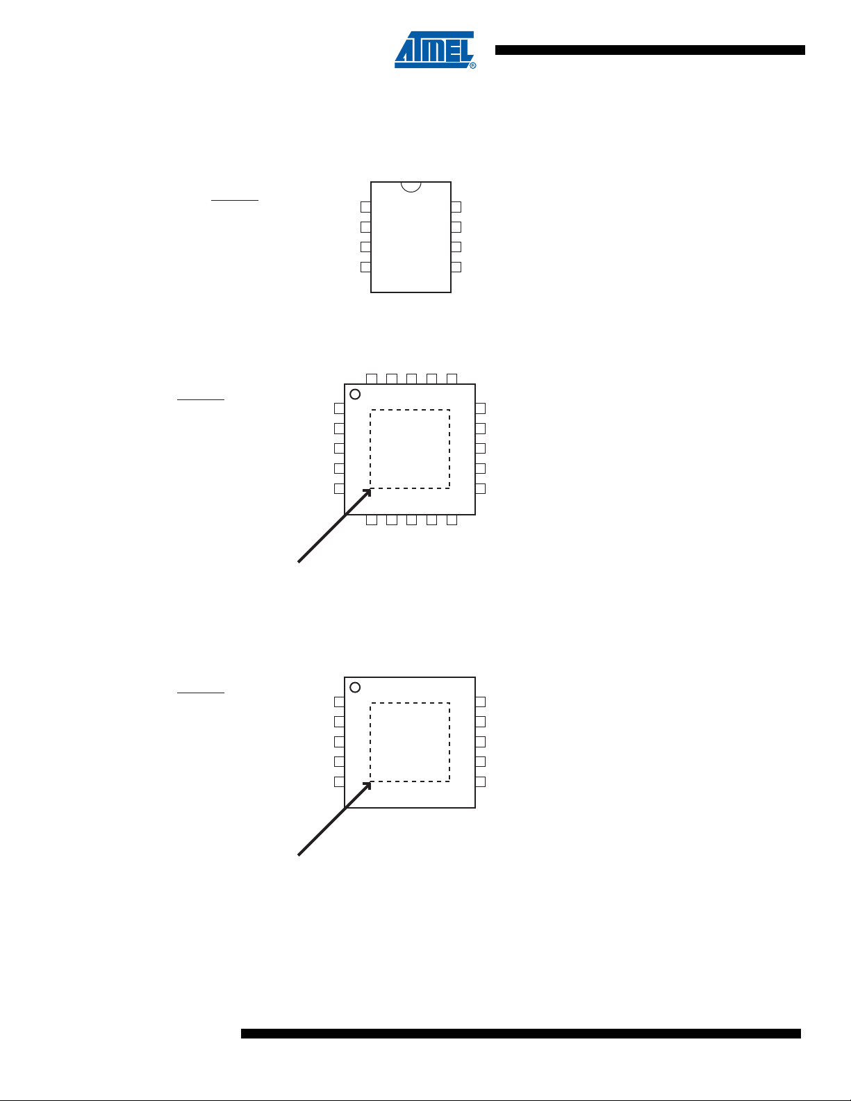
1. Pin Configurations
1
2
3
4
8
7
6
5
(PCINT5/RESET/ADC0/dW) PB5
(PCINT3/CLKI/ADC3) PB3
(PCINT4/ADC2) PB4
GND
VCC
PB2 (SCK/ADC1/T0/PCINT2)
PB1 (MISO/AIN1/OC0B/INT0/PCINT1)
PB0 (MOSI/AIN0/OC0A/PCINT0)
8-PDIP/SOIC
1
2
3
4
5
20-QFN/MLF
15
14
13
12
11
2019181716
6
7
8
9
10
(PCINT5/RESET/ADC0/dW) PB5
(PCINT3/CLKI/ADC3) PB3
DNC
DNC
(PCINT4/ADC2) PB4
DNC
DNC
GND
DNC
DNC
VCC
PB2 (SCK/ADC1/T0/PCINT2)
DNC
PB1 (MISO/AIN1/OC0B/INT0/PCINT1)
PB0 (MOSI/AIN0/OC0A/PCINT0)
DNC
DNC
DNC
DNC
DNC
NOTE: Bottom pad should be soldered to ground.
DNC: Do Not Connect
1
2
3
4
5
10-QFN/MLF
10
9
8
7
6
(PCINT5/RESET/ADC0/dW) PB5
(PCINT3/CLKI/ADC3) PB3
DNC
(PCINT4/ADC2) PB4
GND
VCC
PB2 (SCK/ADC1/T0/PCINT2)
DNC
PB1 (MISO/AIN1/OC0B/INT0/PCINT1)
PB0 (MOSI/AIN0/OC0A/PCINT0)
NOTE: Bottom pad should be soldered to ground.
DNC: Do Not Connect
Figure 1-1. Pinout of ATtiny13A
2
8126BS–AVR–12/08
Page 3

1.1 Pin Description
1.1.1 VCC
Supply voltage.
1.1.2 GND
Ground.
1.1.3 Port B (PB5:PB0)
Port B is a 6-bit bi-directional I/O port with internal pull-up resistors (selected for each bit). The
Port B output buffers have symmetrical drive characteristics with both high sink and source
capability. As inputs, Port B pins that are externally pulled low will source current if the pull-up
resistors are activated. The Port B pins are tri-stated when a reset co ndition becomes active,
even if the clock is not running.
Port B also serves the functions of various special features of the ATtiny13A as listed on page
55.
ATtiny13A
1.1.4
RESET
Reset input. A low level on this pin for longer than the minimum pulse length will generate a
reset, even if the clock is not running and provided the reset pin ha s not been disabled. Th e minimum pulse length is given in Table 18-4 on page 120. Shorter pulses are not guaranteed to
generate a reset.
The reset pin can also be used as a (weak) I/O pin.
8126BS–AVR–12/08
3
Page 4
ATtiny13A
2. Overview
2.1 Block Diagram
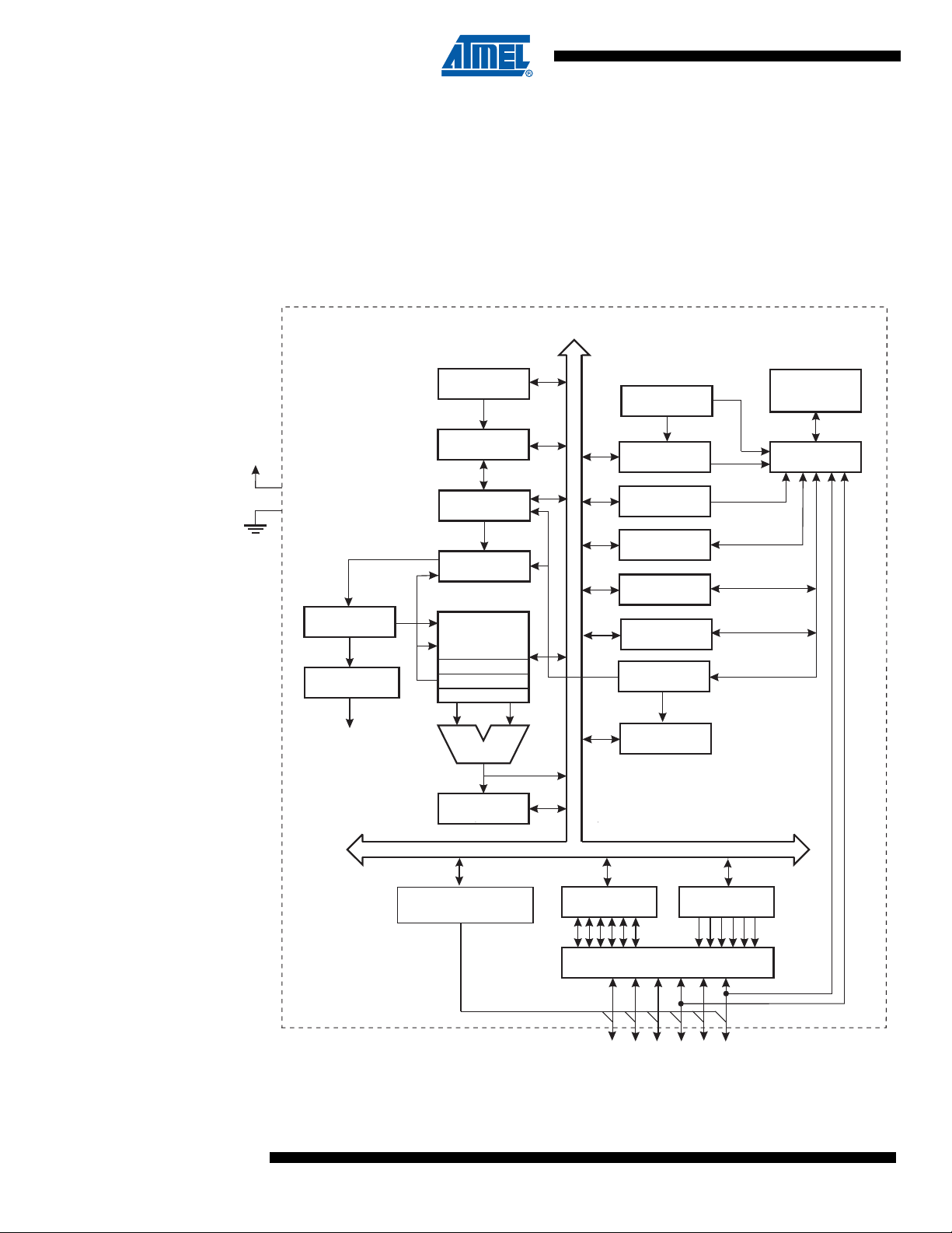
The ATtiny13A is a low-power CMOS 8-bit microcontroller based on the AVR enhanced RISC
architecture. By executing powerful instructions in a single clock cycle, the ATtiny13A achieves
throughputs approaching 1 MIPS pe r MHz allow ing the sy stem de signer to optimize power c onsumption versus processing speed.
Figure 2-1. Block Diagram
8-BIT DATABUS
VCC
GND
INSTRUCTION
REGISTER
INSTRUCTION
DECODER
CONTROL
LINES
STACK
POINTER
SRAM
PROGRAM
COUNTER
PROGRAM
FLASH
GENERAL
PURPOSE
REGISTERS
X
Y
Z
ALU
STATU S
REGISTER
WATCHDOG
OSCILLATOR
WATCHDOG
TIMER
MCU CONTROL
REGISTER
MCU STATUS
REGISTER
TIMER/
COUNTER0
INTERRUPT
UNIT
PROGRAMMING
LOGIC
DATA
EEPROM
CALIBRATED
INTERNAL
TOR
OSCILLA
TIMING AND
CONTROL
4
ADC /
ANALOG COMPARATOR
DATA REGISTER
PORT B
PORT B DRIVERS
PB0-PB5
DATA DIR.
REG.PORT B
RESET
CLKI
8126BS–AVR–12/08
Page 5

ATtiny13A
The AVR core combines a rich instruction set with 32 general purpose working registers. All 32
registers are directly connected to the Arithmetic Logic Unit (ALU), allowing two independent
registers to be accessed in one single instruction executed in one clock cycle. The resulting
architecture is more code efficient while achieving throughputs up to ten times faster than conventional CISC microcontrollers.
The ATtiny13A provides the following feat ures: 1K byte of In -System Programm able Flash, 64
bytes EEPROM, 64 bytes SRAM, 6 general purpose I/O lines, 32 general purpose working registers, one 8-bit Timer/Counter with compare modes, Internal and External Interrupts, a 4channel, 10-bit ADC, a programmable Watchdog Timer with internal Oscillator, and three software selectable power saving modes. The Idle mode stops the CPU while allowing the SRAM,
Timer/Counter, ADC, Analog Comparator, and Interrupt system to continue functioning. The
Power-down mode saves the register contents, disabling all chip functions until the next Interrupt or Hardware Reset. The ADC Noise Reduction mode stops the CPU and all I/O modules
except ADC, to minimize switching noise during ADC conversions.
The device is manufactured using Atmel’s high density non-volatile memory technology. The
On-chip ISP Flash allows the Program memory to be re-programmed In-System through an SPI
serial interface, by a conventional non-volatile memory programmer or by an On-chip boot code
running on the AVR core.
The ATtiny13A AVR is supported with a full suite of program and system development tools
including: C Compilers, Macro Assemblers, Program Debugger/Simulators, and Evaluation kits.
8126BS–AVR–12/08
5
Page 6

ATtiny13A
3. About
3.1 Resources
A comprehensive set of drivers, application notes, data sheet s and descr iption s on development
tools are available for download at http://www.atmel.com/avr.
3.2 Code Examples
This documentation contains simple code examples t hat brief ly show h ow to us e various parts of
the device. These code examples assume that the part specific header file is included b efore
compilation. Be aware that not all C compiler vendors include bit definitions in the header files
and interrupt handling in C is compiler dependent . Please con firm wit h the C com piler d ocume ntation for more details.
3.3 Data Retention
Reliability Qualification results show that the projected data retention failure rate is much less
than 1 PPM over 20 years at 85°C or 100 years at 25⋅C.
6
8126BS–AVR–12/08
Page 7
ATtiny13A
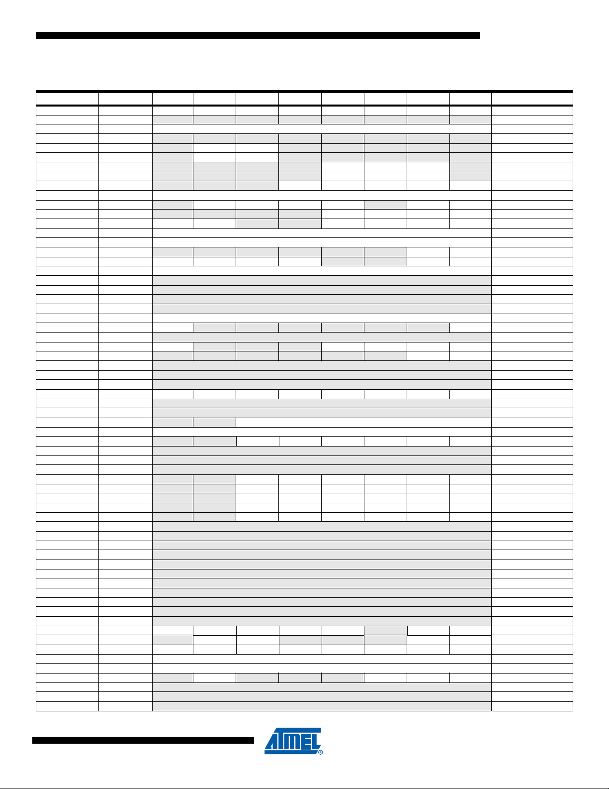
4. Register Summary
Address Name Bit 7 Bit 6 Bit 5 Bit 4 Bit 3 Bit 2 Bit 1 Bit 0 Page
0x3F SREG I T H S V N Z C page 9
0x3E Reserved – – – – – – – –
0x3D SPL SP[7:0] page 11
0x3C Reserved – – – – – – – –
0x3B GIMSK – INT0 PCIE – – – – – page 47
0x3A GIFR – INTF0 PCIF – – – – – page 48
0x39 TIMSK0 – – – – OCIE0B OCIE0A TOIE0 – page 75
0x38 TIFR0 – – – – OCF0B OCF0A TOV0 – page 76
0x37 SPMCSR – – – CTPB RFLB PGWRT PGERS
0x36 OCR0A Timer/Counter – Output Compare Register A page 75
0x35 MCUCR –PUDSESM1SM0 –ISC01ISC00 page 33
0x34 MCUSR – – – – WDRF BORF EXTRF PORF page 42
0x33 TCCR0B FOC0A FOC0B – – WGM02 CS02 CS01 CS00 page 73
0x32 TCNT0 Timer/Counter (8-bit) page 74
0x31 OSCCAL Oscillator Calibration Register page 27
0x30 BODCR – – – – – – BODS BODSE page 33
0x2F TCCR0A COM0A1 COM0A0 COM0B1 COM0B0 – –WGM01WGM00 page 70
0x2E DWDR DWDR[7:0] page 97
0x2D Reserved –
0x2C Reserved –
0x2B Reserved –
0x2A Reserved –
0x29 OCR0B Timer/Counter – Output Compare Register B page 75
0x28 GTCCR TSM – – – – – – PSR10 page 78
0x27 Reserved –
0x26 CLKPR CLKPCE – – – CLKPS3 CLKPS2 CLKPS1 CLKPS0 pa ge 28
0x25 PRR – – – – – – PRTIM0 PRADC page 34
0x24 Reserved –
0x23 Reserved –
0x22 Reserved –
0x21 WDTCR WDTIF WDTIE WDP3 WDCE WDE WDP2 WDP1 WDP0 page 42
0x20 Reserved –
0x1F Reserved –
0x1E EEARL – – EEPROM Address Register page 20
0x1D EEDR EEPROM Data Register page 20
0x1C EECR – – EEPM1 EEPM0 EERIE EEMPE EEPE EERE page 21
0x1B Reserved –
0x1A Reserved –
0x19 Reserved –
0x18 PORTB – – PORTB5 PORTB4 PORTB3 PORTB2 PORTB1 PORTB0 page 57
0x17 DDRB – – DDB5 DDB4 DDB3 DDB2 DDB1 DDB0 page 57
0x16 PINB
0x15 PCMSK – – PCINT5 PCINT4 PCINT3 PCINT2 PCINT1 PCINT0 page 48
0x14 DIDR0
0x13 Reserved
0x12 Reserved –
0x11 Reserved –
0x10 Reserved
0x0F Reserved
0x0E Reserved –
0x0D Reserved
0x0C Reserved
0x0B Reserved –
0x0A Reserved
0x09 Reserved
0x08 ACSR ACD ACBG
0x07 ADMUX – REFS0 ADLAR – – – MUX1 MUX0 page 92
0x06 ADCSRA ADEN ADSC
0x05 ADCH ADC Data Register High Byte page 94
0x04 ADCL ADC Data Register Low Byte page 94
0x03 ADCSRB –ACME– – – ADTS2 ADTS1 ADTS0 page 95
0x02 Reserved
0x01 Reserved
0x00 Reserved –
– – PINB5 PINB4 PINB3 PINB2 PINB1 PINB0 page 58
– – ADC0D ADC2D ADC3D ADC1D AIN1D AIN0D page 81, page 95
–
–
–
–
–
–
–
ACO ACI ACIE – ACIS1 ACIS0 page 80
ADATE ADIF ADIE ADPS2 ADPS1 ADPS0 page 93
–
–
SELFPR-
page 98
8126BS–AVR–12/08
7
Page 8

ATtiny13A
Notes: 1. For compatibility with future devices, reserved bits should be written to zero if accessed. Reserved I/O memory addresses
should never be written.
2. I/O Registers within the address range 0x00 - 0x1F are directly bit-accessible using the SBI and CBI instructions. In these
registers, the value of single bits can be checked by using the SBIS and SBIC instructions.ome of the Status Flags are
cleared by writing a logical one to them. Note that, unlike most other AVRs, the CBI and SBI instructions will only operation
the specified bit, and can therefore be used on registers containing such Status Flags. The CBI and SBI instructions work
with registers 0x00 to 0x1F only.
8
8126BS–AVR–12/08
Page 9
ATtiny13A
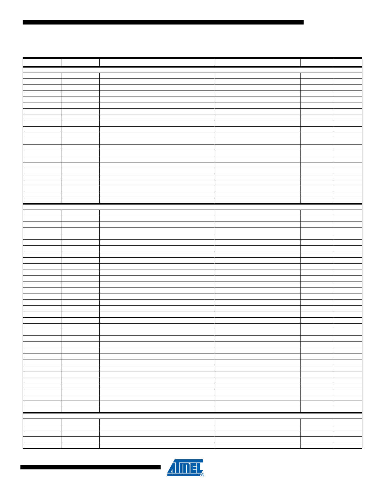
5. Instruction Set Summary
Mnemonics Operands Description Operation Flags #Clocks
ADD Rd, Rr Add two Registers Rd ← Rd + Rr Z,C,N,V,H 1
ADC Rd, Rr Add with Carry two Registers Rd ← Rd + Rr + C Z,C,N,V,H 1
ADIW Rdl,K Add Immediate to Word Rdh:Rdl ← Rdh:Rdl + K Z,C,N,V,S 2
SUB Rd, Rr Subtract two Registers Rd ← Rd - Rr Z,C,N,V,H 1
SUBI Rd, K Subtract Constant from Register Rd ← Rd - K Z,C,N,V,H 1
SBC Rd, Rr Subtract with Carry two Registers Rd ← Rd - Rr - C Z,C,N,V,H 1
SBCI Rd, K Subtract with Carry Constant from Reg. Rd ← Rd - K - C Z,C,N,V,H 1
SBIW Rdl,K Subtract Immediate from Word Rdh:Rdl ← Rdh:Rdl - K Z,C,N,V,S 2
AND Rd, Rr Logical AND Registers Rd ← Rd • Rr Z,N,V 1
ANDI Rd, K Logical AND Register and Constant Rd ← Rd • K Z,N,V 1
OR Rd, Rr Logical OR Registers Rd ← Rd v Rr Z,N,V 1
ORI Rd, K Logical OR Register and Constant Rd ← Rd v K Z,N,V 1
EOR Rd, Rr Exclusive OR Registers Rd ← Rd ⊕ Rr Z,N,V 1
COM Rd One’s Complement Rd ← 0xFF − Rd Z,C,N,V 1
NEG Rd Two’s Complement Rd ← 0x00 − Rd Z,C,N,V,H 1
SBR Rd,K Set Bit(s) in Register Rd ← Rd v K Z,N,V 1
CBR Rd,K Clear Bit(s) in Register Rd ← Rd • (0xFF - K) Z,N,V 1
INC Rd Increment Rd ← Rd + 1 Z,N,V 1
DEC Rd Decrement Rd ← Rd − 1 Z,N,V 1
TST Rd Test for Zero or Minus Rd ← Rd • Rd Z,N,V 1
CLR Rd Clear Register Rd ← Rd ⊕ Rd Z,N,V 1
SER Rd Set Register Rd ← 0xFF None 1
RJMP k Relative Jump PC ← PC + k + 1 None 2
IJMP Indirect Jump to (Z) PC ← Z None 2
RCALL k Relative Subroutine Call PC ← PC + k + 1 None 3
ICALL Indirect Call to (Z) PC ← ZNone3
RET Subroutine Return PC ← STACK None 4
RETI Interrupt Return PC ← STACK I 4
CPSE Rd,Rr Compare, Skip if Equal if (Rd = Rr) PC ← PC + 2 or 3 None 1/2/3
CP Rd,Rr Compare Rd − Rr Z, N,V,C,H 1
CPC Rd,Rr Compare with Carry Rd − Rr − C Z, N,V,C,H 1
CPI Rd,K Compare Register with Immediate Rd − K Z, N,V,C,H 1
SBRC Rr, b Skip if Bit in Register Cleared if (Rr(b)=0) PC ← PC + 2 or 3 None 1/2/3
SBRS Rr, b Skip if Bit in Register is Set if (Rr(b)=1) PC ← PC + 2 or 3 None 1/2/3
SBIC P, b Skip if Bit in I/O Register Cleared if (P(b)=0) PC ← PC + 2 or 3 None 1/2/3
SBIS P, b Skip if Bit in I/O Register is Set if (P(b)=1) PC ← PC + 2 or 3 None 1/2/3
BRBS s, k Branch if Status Flag Set if (SREG(s) = 1) then PC←PC+k + 1 None 1/2
BRBC s, k Branch if Status Flag Cleared if (SREG(s) = 0) then PC←PC+k + 1 None 1/2
BREQ k Branch if Equal if (Z = 1) then PC ← PC + k + 1 None 1/2
BRNE k Branch if Not Equal if (Z = 0) then PC ← PC + k + 1 None 1/2
BRCS k Branch if Carry Set if (C = 1) then PC ← PC + k + 1 None 1/2
BRCC k Branch if Carry Cleared if (C = 0) then PC ← PC + k + 1 None 1/2
BRSH k Branch if Same or Higher if (C = 0) then PC ← PC + k + 1 None 1/2
BRLO k Branch if Lower if (C = 1) then PC ← PC + k + 1 None 1/2
BRMI k Branch if Minus if (N = 1) then PC ← PC + k + 1 None 1/2
BRPL k Branch if Plus if (N = 0) then PC ← PC + k + 1 None 1/2
BRGE k Branch if Greater or Equal, Signed if (N ⊕ V= 0) then PC ← PC + k + 1 N one 1/2
BRLT k Branch if Less Than Zero, Signed if (N ⊕ V= 1) then PC ← PC + k + 1 None 1/2
BRHS k Branch if Half Carry Flag Set if (H = 1) then PC ← PC + k + 1 None 1/2
BRHC k Branch if Half Carry Flag Cleared if (H = 0) then PC ← PC + k + 1 None 1/2
BRTS k Branch if T Flag Set if (T = 1) then PC ← PC + k + 1 None 1/2
BRTC k Branch if T Flag Cleared if (T = 0) then PC ← PC + k + 1 None 1/2
BRVS k Branch if Overflow Flag is Set if (V = 1) then PC ← PC + k + 1 None 1/2
BRVC k Branch if Overflow Flag is Cleared if (V = 0) then PC ← PC + k + 1 None 1/2
BRIE k Branch if Interrupt Enabled if ( I = 1) then PC ← PC + k + 1 None 1/2
BRID k Branch if Interrupt Disabled if ( I = 0) then PC ← PC + k + 1 None 1/2
SBI P,b Set Bit in I/O Register I/O(P,b) ← 1None2
CBI P,b Clear Bit in I/O Register I/O(P,b) ← 0None2
LSL Rd Logical Shift Left Rd(n+1) ← Rd(n), Rd(0) ← 0 Z,C,N,V 1
LSR Rd Logical Shift Right Rd(n) ← Rd(n+1), Rd(7) ← 0 Z,C,N,V 1
ROL Rd Rotate Left Through Carry Rd(0)←C,Rd(n+1)← Rd(n),C←Rd(7) Z,C,N,V 1
ARITHMETIC AND LOGIC INSTRUCTIONS
BRANCH INSTRUCTIONS
BIT AND BIT-TEST INSTRUCTIONS
8126BS–AVR–12/08
9
Page 10
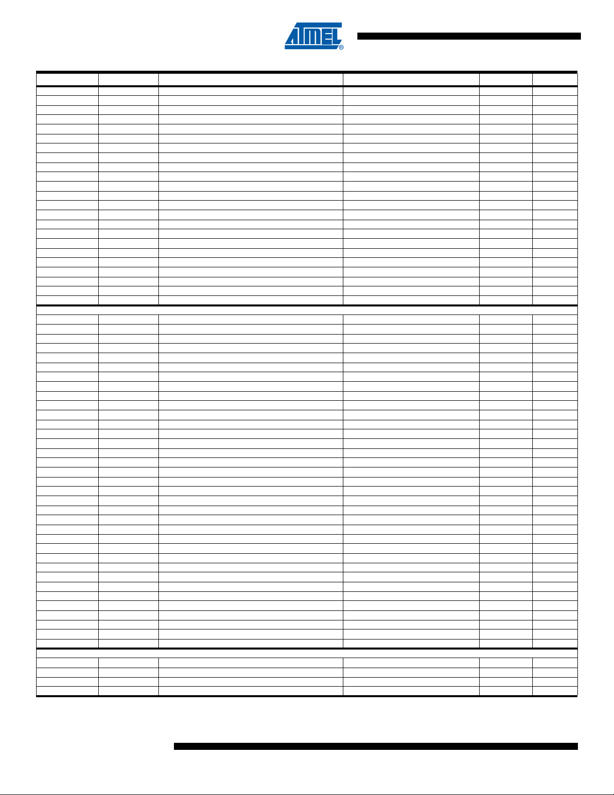
ATtiny13A
Mnemonics Operands Description Operation Flags #Clocks
ROR Rd Rotate Right Through Carry Rd(7)←C,Rd(n)← Rd(n+1),C←Rd(0) Z,C,N,V 1
ASR Rd Arithmetic Shift Right Rd(n) ← Rd(n+1), n= 0..6 Z,C,N,V 1
SWAP Rd Swap Nibbles Rd(3..0)←Rd(7..4),Rd(7..4)←Rd(3..0) None 1
BSET s Flag Set SREG(s) ← 1 SREG(s) 1
BCLR s Flag Clear SREG(s) ← 0 SREG(s) 1
BST Rr, b Bit Store from Register to T T ← Rr(b) T 1
BLD Rd, b Bit load from T to Register Rd(b) ← TNone1
SEC Set Carry C ← 1C1
CLC Clear Carry C ← 0 C 1
SEN Set Negative Flag N ← 1N1
CLN Clear Negative Flag N ← 0 N 1
SEZ Set Zero Flag Z ← 1Z1
CLZ Clear Zero Flag Z ← 0 Z 1
SEI Global Interrupt Enable I ← 1I1
CLI Global Interrupt Disable I ← 0 I 1
SES Set Signed Test Flag S ← 1S1
CLS Clear Signed Test Flag S ← 0 S 1
SEV Set Twos Complement Overflow. V ← 1V1
CLV Clear Twos Complement Overflow V ← 0 V 1
SET Set T in SREG T ← 1T1
CLT Clear T in SREG T ← 0 T 1
SEH Set Half Carry Flag in SREG H ← 1H1
CLH Clear Half Carry Flag in SREG H ← 0 H
MOV Rd, Rr Move Between Registers Rd ← Rr None 1
MOVW Rd, Rr Copy Register Word
LDI Rd, K Load Immediate Rd ← KNone1
LD Rd, X Load Indirect Rd ← (X) None 2
LD Rd, X+ Load Indirect and Post-In c. Rd ← (X), X ← X + 1 None 2
LD Rd, - X Load Indirect and Pre-Dec. X ← X - 1, Rd ← (X) None 2
LD Rd, Y Load Indirect Rd ← (Y) None 2
LD Rd, Y+ Load Indirect and Post-In c. Rd ← (Y), Y ← Y + 1 None 2
LD Rd, - Y Load Indirect and Pre-Dec. Y ← Y - 1, Rd ← (Y) None 2
LDD Rd,Y+q Load Indirec t with Displacement Rd ← (Y + q) None 2
LD Rd, Z Load Indirect Rd ← (Z) None 2
LD Rd, Z+ Load Indirect and Post-Inc. Rd ← (Z), Z ← Z+1 None 2
LD Rd, -Z Load Indirect and Pre-Dec. Z ← Z - 1, Rd ← (Z) None 2
LDD Rd, Z+q Load Indirect with Displacement Rd ← (Z + q) Non e 2
LDS Rd, k Load Direct from SRAM Rd ← (k) None 2
ST X, Rr Store Indirect (X) ← Rr None 2
ST X+, Rr Store Indirect and Post-Inc. (X) ← Rr , X ← X + 1 None 2
ST - X, Rr Store Indirect and Pre-Dec. X ← X - 1, (X) ← Rr None 2
ST Y, Rr Store Indirect (Y) ← Rr None 2
ST Y+, Rr Store Indirect and Post-Inc. (Y) ← Rr, Y ← Y + 1 None 2
ST - Y, Rr Store Indirect and Pre-Dec. Y ← Y - 1, (Y) ← Rr None 2
STD Y+q,Rr Store Indirect with Displacement (Y + q) ← Rr None 2
ST Z, Rr Store Indirect (Z) ← Rr None 2
ST Z+, Rr Store Indirect and Post-Inc. (Z) ← Rr, Z ← Z + 1 None 2
ST -Z, Rr Store Indirect and Pre-Dec. Z ← Z - 1, (Z) ← Rr None 2
STD Z+q,Rr Store Indirect with Displacement (Z + q) ← Rr None 2
STS k, Rr Store Direct to SRAM (k) ← Rr None 2
LPM Load Program Memory R0 ← (Z) None 3
LPM Rd, Z Load Program Memory Rd ← (Z) None 3
LPM Rd, Z+ Load Program Memory and Post-Inc Rd ← (Z), Z ← Z+1 None 3
SPM Store Program Memory (z) ← R1:R0 None
IN Rd, P In Port Rd ← PNone1
OUT P, Rr Out Port P ← Rr None 1
PUSH Rr Push Register on Stack STACK ← Rr None 2
POP Rd Pop Register from Stack Rd ← STACK None 2
NOP No Operation None 1
SLEEP Sleep (see specific descr. for Sleep func tion) None 1
WDR Watchdog Reset (see specific descr. for WDR/Timer) None 1
BREAK Break For On-chip Debug Only None N/A
DATA TRANSFER INSTRUCTIONS
MCU CONTROL INSTRUCTIONS
Rd+1:Rd ← Rr+1:Rr
None 1
1
10
8126BS–AVR–12/08
Page 11
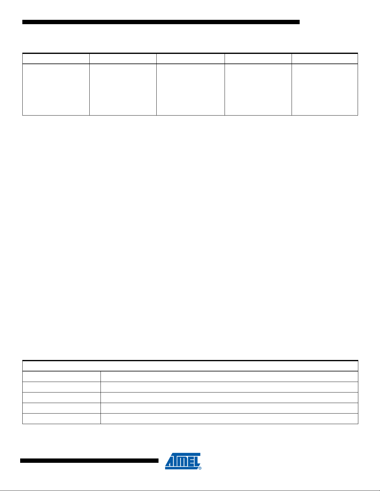
6. Ordering Information
Speed (MHz)
Notes: 1. For device speed vs. VCC, see “Speed Grades” on page 118.
2. This device can also be supplied in wafer f orm. Please contact your local Atmel sales office for detailed ordering information
3. All packages are Pb-free, Halide-free, fully green and they comply with the European directive for Restriction of Hazardous
(1)
20 1.8 - 5.5
and minimum quantities.
Substances (RoHS).
Power Supply (V)
(1)
Ordering Code Package
ATtiny13A-PU
ATtiny13A-SU
ATtiny13A-SH
ATtiny13A-SSU
ATtiny13A-SSH
ATtiny13A-MU
ATtiny13A-MMU
8P3
8S2
8S2
8S1
8S1
20M1
10M1
(2) (3)
ATtiny13A
Operation Range
Industrial
(-40⋅C to 85⋅C)
Package Type
8P3 8-lead, 0.300" Wide, Plastic Dual Inline Package (PDIP)
8S2 8-lead, 0.209" Wide, Plastic Small Outline Package (EIAJ SOIC)
8S1 8-lead, 0.150" Wide, Plastic Gull-Wing Small Outline (JEDEC SOIC)
20M1
10M1
8126BS–AVR–12/08
20-pad, 4 x 4 x 0.8 mm Body, Lea d Pitch 0.50 mm, Micro Lead Frame Package (MLF)
10-pad, 3 x 3 x 1 mm Body, Le ad Pitch 0.50 mm, Micro Lead Frame Package (MLF)
11
Page 12
ATtiny13A
7. Packaging Information
2325 Orchard Parkway
San Jose, CA 95131
TITLE
DRAWING NO.
R
REV.
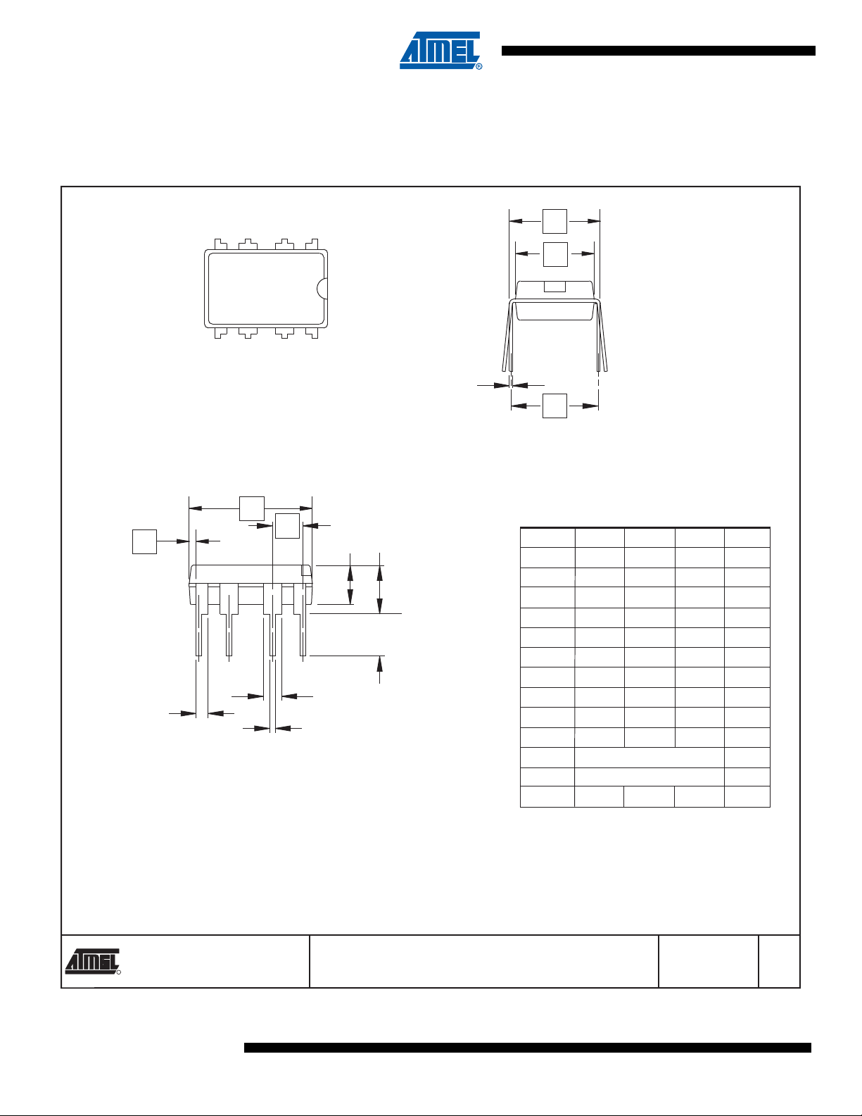
8P3, 8-lead, 0.300" Wide Body, Plastic Dual
In-line Package (PDIP)
01/09/02
8P3
B
D
D1
E
E1
e
L
b2
b
A2 A
1
N
eA
c
b3
4 PLCS
Top View
Side View
End View
COMMON DIMENSIONS
(Unit of Measure = inches)
SYMBOL
MIN
NOM
MAX
NOTE
Notes: 1. This drawing is for general information only; refer to JEDEC Drawing MS-001, Variation BA for additional information.
2. Dimensions A and L are measured with the package seated in JEDEC seating plane Gauge GS-3.
3. D, D1 and E1 dimensions do not include mold Flash or protrusions. Mold Flash or protrusions shall not exceed 0.010 inch.
4. E and eA measured with the leads constrained to be perpendicular to datum.
5. Pointed or rounded lead tips are preferred to ease insertion.
6. b2 and b3 maximum dimensions do not include Dambar protrusions. Dambar protrusions shall not exceed 0.010 (0.25 mm).
A 0.210 2
A2 0.115 0.130 0.195
b 0.014 0.018 0.022 5
b2 0.045 0.060 0.070 6
b3 0.030 0.039 0.045 6
c 0.008 0.010 0.014
D 0.355 0.365 0.400 3
D1 0.005 3
E 0.300 0.310 0.325 4
E1 0.240 0.250 0.280 3
e 0.100 BSC
eA 0.300 BSC 4
L 0.115 0.130 0.150 2
7.1 8P3
12
8126BS–AVR–12/08
Page 13
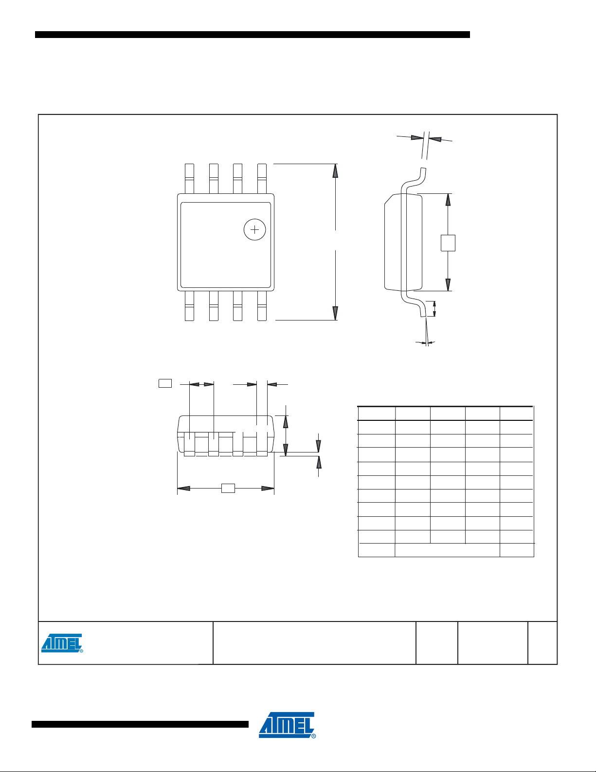
7.2 8S2
TITLE
DRAWING NO. GPC
REV.
Package Drawing Contact:
[email protected]
8S2STN F
8S2, 8-lead, 0.208” Body, Plastic Small
Outline Package (EIAJ)
4/15/08
COMMON DIMENSIONS
(Unit of Measure = mm)
SYMBOL
MIN
NOM
MAX
NOTE
Notes: 1. This drawing is for general information only; refer to EIAJ Drawing EDR-7320 for additional information.
2. Mismatch of the upper and lower dies and resin burrs aren't included.
3. Determines the true geometric position.
4. Values b,C apply to plated terminal. The standard thickness of the plating layer shall measure between 0.007 to .021 mm.
A 1.70 2.16
A1 0.05 0.25
b 0.35 0.48 4
C 0.15 0.35 4
D 5.13 5.35
E1 5.18 5.40 2
E 7.70 8.26
L 0.51 0.85
θ 0° 8°
e 1.27 BSC 3
θθ
11
NN
EE
TOP VIEWTOP VIEW
CC
E1E1
END VIEWEND VIEW
AA
bb
LL
A1A1
ee
DD
SIDE VIEWSIDE VIEW
ATtiny13A
8126BS–AVR–12/08
13
Page 14
ATtiny13A
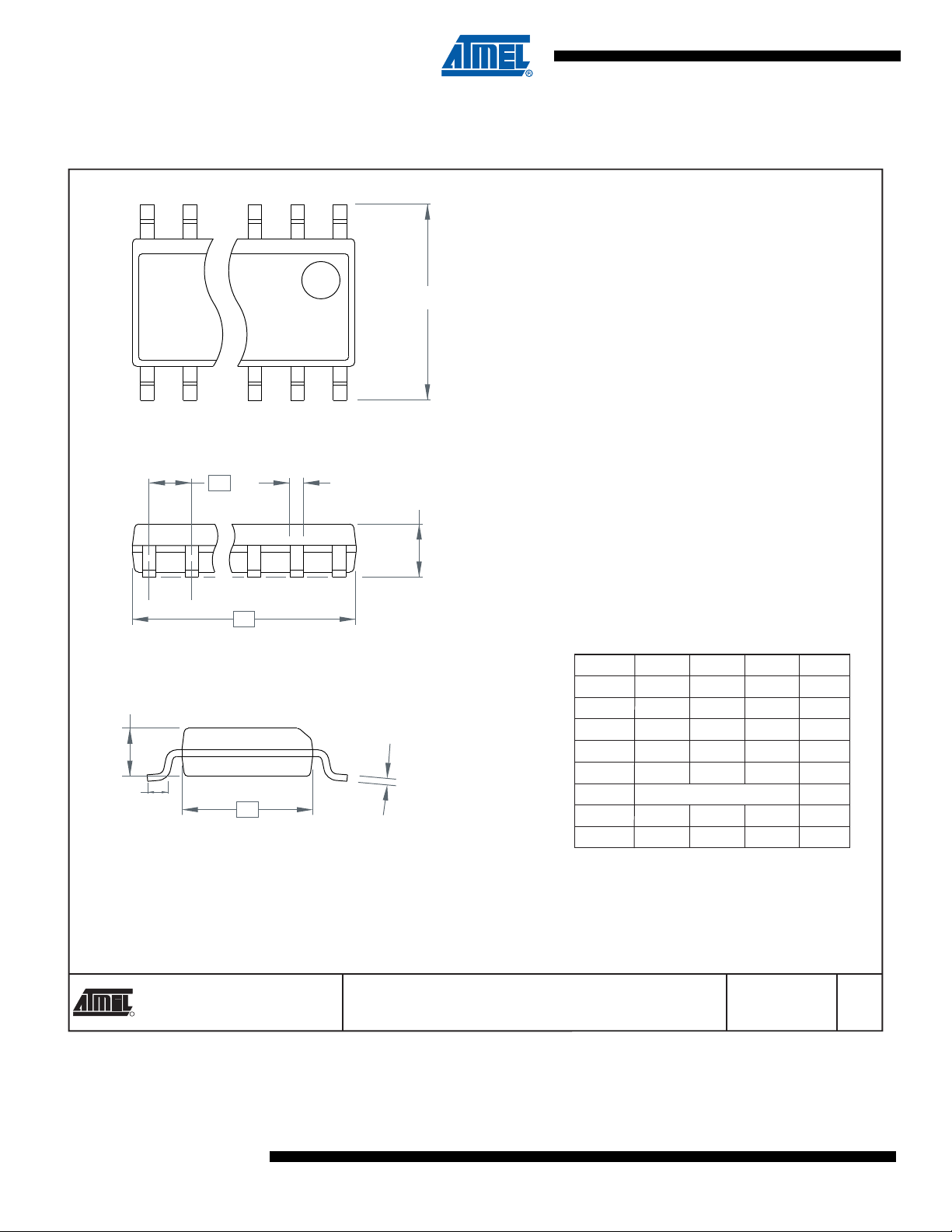
7.3 8S1
2325 Orchard Parkway
San Jose, CA 95131
TITLE
DRAWING NO.
R
REV.
Note:
10/10/01
8S1, 8-lead (0.150" Wide Body), Plastic Gull Wing
Small Outline (JEDEC SOIC)
8S1 A
H
1
2
N
3
Top View
C
E
End View
A
B
L
A2
e
D
Side View
COMMON DIMENSIONS
(Unit of Measure = mm)
SYMBOL
MIN
NOM
MAX
NOTE
This drawing is for general information only. Refer to JEDEC Drawing MS-012 for proper dimensions, tolerances, datums, etc.
A – – 1.75
B – – 0.51
C – – 0.25
D – – 5.00
E – – 4.00
e 1.27 BSC
H – – 6.20
L – – 1.27
14
8126BS–AVR–12/08
Page 15
7.4 20M1
2325 Orchard Parkway
San Jose, CA 95131
TITLE
DRAWING NO.
R
REV.
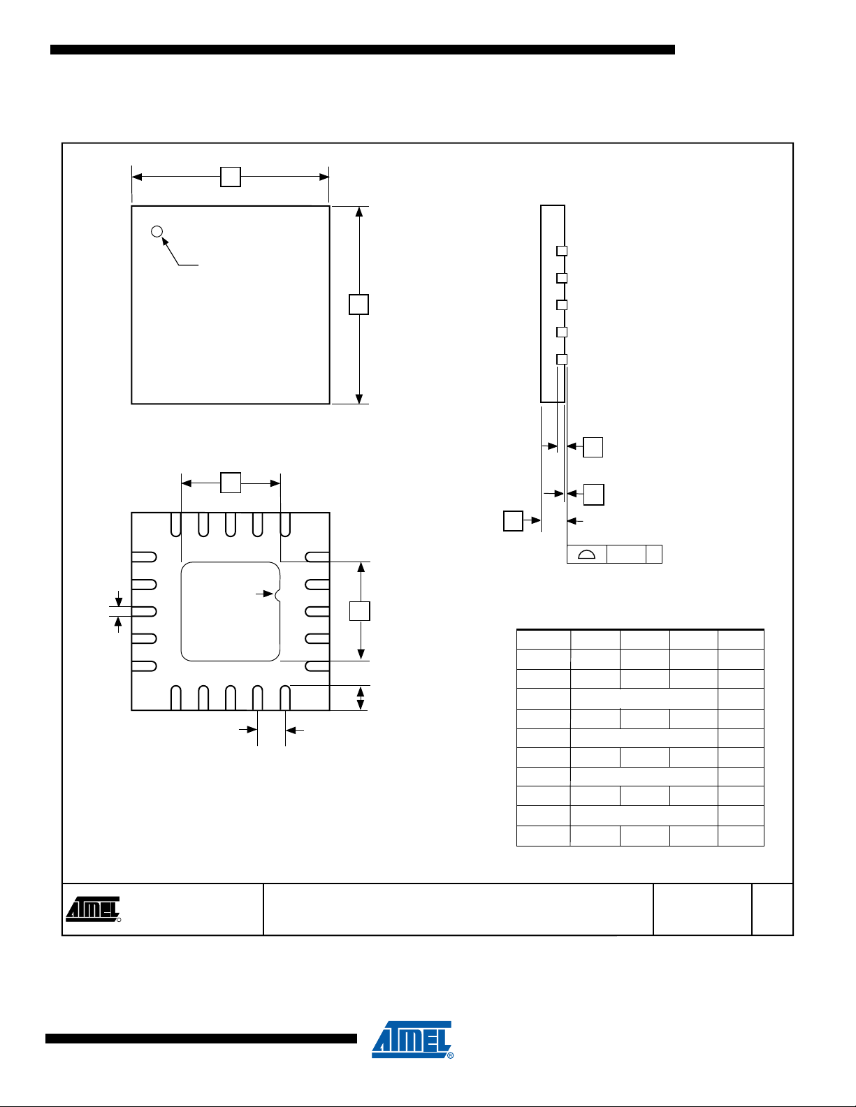
20M1, 20-pad, 4 x 4 x 0.8 mm Body, Lead Pitch 0.50 mm,
A
20M1
10/27/04
2.6 mm Exposed Pad, Micro Lead Frame Package (MLF)
A 0.70 0.75 0.80
A1 – 0.01 0.05
A2 0.20 REF
b 0.18 0.23 0.30
D 4.00 BSC
D2 2.45 2.60 2.75
E 4.00 BSC
E2 2.45 2.60 2.75
e 0.50 BSC
L 0.35 0.40 0.55
SIDE VIEW
Pin 1 ID
Pin #1
Notch
(0.20 R)
BOTTOM VIEW
TOP VIEW
Note:
Reference JEDEC Standard MO-220, Fig. 1 (SAW Singulation) WGGD-5.
COMMON DIMENSIONS
(Unit of Measure = mm)
SYMBOL
MIN
NOM
MAX
NOTE
D
E
e
A2
A1
A
D2
E2
0.08
C
L
1
2
3
b
1
2
3
ATtiny13A
8126BS–AVR–12/08
15
Page 16
ATtiny13A
7.5 10M1
2325 Orchard Parkway
San Jose, CA 95131
TITLE
DRAWING NO.
R
REV.
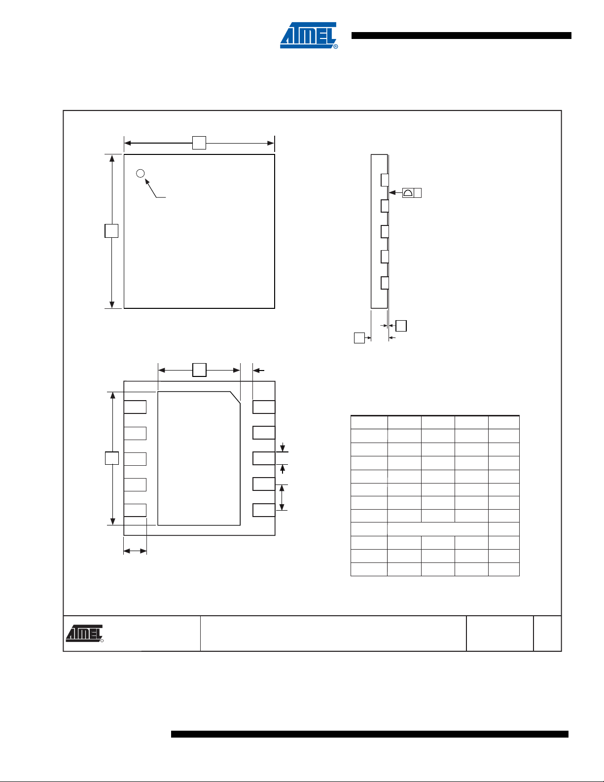
10M1, 10-pad, 3 x 3 x 1.0 mm Body, Lead Pitch 0.50 mm,
1.64 x 2.60 mm Exposed Pad, Micro Lead Frame Package
A
10M1
7/7/06
COMMON DIMENSIONS
(Unit of Measure = mm)
SYMBOL
MIN
NOM
MAX
NOTE
A 0.80 0.90 1.00
A1 0.00 0.02 0.05
b 0.18 0.25 0.30
D 2.90 3.00 3.10
D1 1.40 – 1.75
E 2.90 3.00 3.10
E1 2.20 – 2.70
e 0.50
L 0.30 – 0.50
y – – 0.08
K 0.20 – –
Pin 1 ID
TOP VIEW
D
E
A1
A
SIDE VIEW
BOTTOM VIEW
D1
E1
L
b
e
K
1
2
Notes: 1. This package conforms to JEDEC reference MO-229C, Variation VEED-5.
2. The terminal #1 ID is a Lasser-marked Feature.
y
16
8126BS–AVR–12/08
Page 17

8. Errata
The revision letters in this section refer to the revision of the ATtiny13A device.
8.1 ATtiny13A Rev. G – H
No known errata.
8.2 ATtiny13A Rev. E – F
These device revisions were not sampled.
8.3 ATtiny13A Rev. A – D
These device revisions were referred to as ATtiny13/ATtiny13V.
ATtiny13A
8126BS–AVR–12/08
17
Page 18

ATtiny13A
9. Datasheet Revision History
Please note that page numbers in this section refer to the current version of this document and
may not apply to previous versions.
9.1 Rev. 8126B – 11/08
1. Updated order codes on page 11 to reflect changes in material composition.
2. Updated sections:
– “DIDR0 – Digital Input Disable Register 0” on page 81
– “DIDR0 – Digital Input Disable Register 0” on page 95
3. Updated “Register Summary” on page 7 .
9.2 Rev. 8126A – 05/08
1. Initial revision, created from document 2535I – 04/08.
2. Updated characteristic plots of section “Typical Characteristics” , starting on page 124.
3. Updated “Ordering Information” on page 11.
4. Updated section:
– “Speed Grades” on page 118
5. Update tables:
– “DC Characte ristics, T
– “Calibration Accuracy of Internal RC Oscillator” on page 119
– “Reset, Bro wn-out, and Internal Voltage Characteristics” on page 120
– “ADC Characteristics, Single Ended Channels. TA = -40⋅C - 85⋅C” on page 121
– “Serial Programming Characteristics, T
6. Added description of new function, “Power Reduction Register”:
– Added functional description on page 31
– Added bit description on page 34
– Added section “Supply Current of I/O Modules” on page 124
– Updated Register Summary on page 7
7. Added description of new funct ion, “Software BOD Disable”:
– Added functional description on page 31
– Updated section on page 32
– Added register description on page 33
– Updated Register Summary on page 7
8. Added description of enhanced function, “Enhanced Power-On Reset”:
– Updated Table 18-4 on page 120, and Table 18-5 on page 120
= -40⋅C to 85⋅C” on page 117
A
= -40⋅C to 85⋅C” on page 122
A
18
8126BS–AVR–12/08
Page 19

ATtiny13A
8126BS–AVR–12/08
19
Page 20

Headquarters International
Atmel Corporation
2325 Orchard Parkway
San Jose, CA 95131
USA
Tel: 1(408) 441-0311
Fax: 1(408) 487-2600
Atmel Asia
Unit 1-5 & 16, 19/F
BEA Tower, Millennium City 5
418 Kwun Tong Road
Kwun Tong, Kowloon
Hong Kong
Tel: (852) 2245-6100
Fax: (852) 2722-1369
Product Contact
Web Site
www.atmel.com
Literature Requests
www.atmel.com/literature
Atmel Europe
Le Krebs
8, Rue Jean-Pierre Timbaud
BP 309
78054 Saint-Quentin-enYvelines Cedex
France
Tel: (33) 1-30-60-70-00
Fax: (33) 1-30-60-71-11
Technical Support
Atmel Japan
9F, Tonetsu Shinkawa Bldg.
1-24-8 Shinkawa
Chuo-ku, Tokyo 104-0033
Japan
Tel: (81) 3-3523-3551
Fax: (81) 3-3523-7581
Sales Contact
www.atmel.com/contacts
Disclaimer: The information in this document is provided in connection with Atmel products. No license, express or implied, by estoppel or otherwise, to any
intellectual property right is granted by this document or in conne ction with the sale of Atmel products. EXCEPT AS SET FORTH IN ATMEL’S TERMS AND CONDI-
TIONS OF SALE LOCATED ON ATMEL’S WEB SITE, ATMEL ASSUMES NO LIABILITY WHATSOEVER AND DISCLAIMS ANY EXPRESS, IMPLIED OR STATUTORY
WARRANTY RELATING TO ITS PRODUCTS INCLUDING, BUT NOT LIMITED TO, THE IMPLIED WARRANTY OF MERCHANTABILITY, FITNESS FOR A PARTICULAR
PURPOSE, OR NON-INFRINGEMENT. IN NO EVENT SHALL ATMEL BE LIABLE FOR ANY DIRECT, INDIRECT, CONSEQUENTIAL, PUNITIVE, SPECIAL OR INCIDENT AL DAMAGES (INCLUDING, WITHOUT LIMITATION, D AMAGES FOR LOSS OF PROFITS, BUSINESS INTERRUPTION, OR LOSS OF INF ORMATION) ARISING OUT OF
THE USE OR INABILITY TO USE THIS DOCUMENT, EVEN IF ATMEL HAS BEEN ADVISED OF THE POSSIBILITY OF SUCH DAMAGES. Atmel makes no
representations or warranties with respect to the accuracy or completeness of the contents of this document and reserves the right to make changes to specifications
and product descriptions at any time without notice. Atmel does not make any commitment to update the information contained here in. Unless specifically provided
otherwise, Atmel products are not suitable for, and shall not be used in, automotive applications. Atmel’s products are not intended, authorized, or warranted for use
as components in applications intended to suppor t or sustain life.
© 2008 Atmel Corporation. All rights reserved. Atmel®, logo and combinations thereof, AVR® and others are registered trademarks or trade-
marks of Atmel Corporation or its subsidiaries. Other term s and product names may be trademarks of others.
8126BS–AVR–12/08
 Loading...