

Page 1
Features
• Frequency Range 5 GHz to 6 GHz
• P
25 dBm at 5.8 GHz
out
• Gain Typically 30 dB
• P
Typically 0 dBm
in
• V
2.7V to 3.8V
CC
• Power Consumption in Power-down Mode Typically < 1 µA
• Package: QFN16 3 mm × 3 mm
Benefits
• Biasing Control Extends Battery Time
• Simple Input and Output Matching
• Only One Single Supply Required
• No High-side Switching Transistor Required
1. Description
1.1 Process
This 5-GHz power amplifier (PA) is designed using Atmel’s Silicon-Germanium (SiGe)
process and provides high efficiency.
5.8 GHz WDCT
Power Amplifier
ATR7040
1.2 Circuitry
The PA, ATR7040, consists of a three-stage amplifier with a typical output power of
25 dBm. The output stage was implemented using an open-collector structure. Power
up, power down, and output level are controlled at bias control pin 6 (V
).
ctl
4868C–DECT–05/06
Page 2
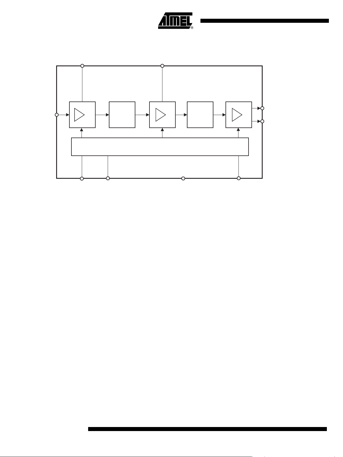
Figure 1-1. Block Diagram
RFIN
10
VCC1
7
13
VCTL
VCC2
6
ATR7040
Matching Matching
Bias control
14
GND
PADDLE
GND
RFOUT/VCC3
2
RFOUT/VCC3
3
15
VCC_CTL
2
ATR7040
4868C–DECT–05/06
Page 3
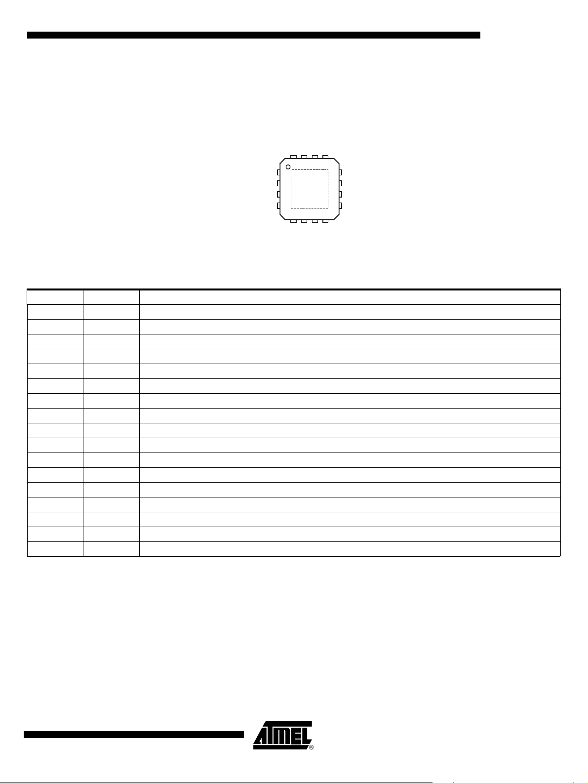
2. Pin Configuration
Figure 2-1. Pinning QFN16
NC
RFOUT/VCC3
RFOUT/VCC3
NC
VCC_CTL
NC
16 15 14 13
1
ATR7040
2
3
GND on the
PADDLE
4
5 6 7 8
GND
VCTL
12
11
10
9
ATR7040
NC
NC
RFIN
NC
NC
Table 2-1. Pin Description
Pin Symbol Function
1 NC Not connected
2 RFOUT RF output and supply voltage for output amplifier stage
3 RFOUT RF output and supply voltage for output amplifier stage
4 NC Not connected
5 NC Not connected
6 VCC2 Supply voltage for second amplifier stage
7 VCC1 Supply voltage for first amplifier stage
8 NC Not connected
9 NC Not connected
10 RFIN RF input
11 NC Not connected
12 NC Not connected
13 VCTL Control voltage for power ramping
14 GND Ground
15 VCC_CTL Supply voltage for biasing control block
16 NC Not connected
PADDLE – Ground
Note: 1. Pin can be connected to paddle for increased GND area
(1)
(1)
(1)
(1)
(1)
(1)
(1)
(1)
VCC1
VCC2
NC
4868C–DECT–05/06
3
Page 4

3. Absolute Maximum Ratings
Stresses beyond those listed under “Absolute Maximum Ratings” may cause permanent damage to the device. This is a stress rating
only and functional operation of the device at these or any other conditions beyond those indicated in the operational sections of this
specification is not implied. Exposure to absolute maximum rating conditions for extended periods may affect device reliability.
Parameters Symbol Value Unit
Supply voltage V
Supply current I
Junction temperature T
Storage temperature T
Input RF power P
Control voltage V
CC
cc
j
Stg
in
ctl
5V
400 mA
150 °C
–40 to +125 °C
10 dBm
2.5 V
Note: The part may not survive all maximums applied simultaneously.
Electrostatic sensitive device.
Observe precautions for handling.
4. Thermal Resistance
Parameters Symbol Value Unit
Junction ambient package QFN16, 3 × 3,
slug soldered on PCB
R
thJA
40 K/W
5. Operating Range
Parameters Symbol Value Unit
Supply voltage V
Operating frequency range f
Ambient temperature range T
CC
in
amb
2.7 to 3.8 V
5100 to 5900 MHz
–25 to +75 °C
4
ATR7040
4868C–DECT–05/06
Page 5

ATR7040
T
6. Electrical Characteristics
Operating conditions: VCC = 3.6V, V
= 25°C, unless otherwise specified.
T
amb
No. Parameters Test Conditions Pin Symbol Min. Typ. Max. Unit
1.0 Frequency range
1.1 Supply voltage V
1.2 Input power P
1.3 Saturated power output P
1.4 Output power deviation P
1.5 Control voltage range
1.6 Control input current PA on 5 I
1.7 Input return loss With external matching 10 –7 –6 dB
1.8 Isolation V
1.9 Power added efficiency
1.10 Current consumption For 25 dBm output power I
1.11
Current consumption in
power-down mode
1.12 Duty cycle of operation At saturated output power 100 %
= 1.5V, input frequency = 5.8 GHz, input power 0 dBm, pulsed mode, duty cycle 10%, ton = 1 ms,
ctl
Depends on external
circuitry
PA operating mode V
Power-down mode V
≤ 0.2V ISO
ctl
At power saturation,
=0dBm
P
in
≤ 0.2V I
V
ctl
PA E 3 5 %
cc
in
25 dBm
sat
d
ctl
ctl
ctl
r
cc
cc
5100 5900 MHz
2.7 3.6 3.8 V
0dBm
–2 +2 dB
1.0 1.7 V
0.2 V
90 µA
33 35 dB
250 mA
1µA
7. Application Circuit
Figure 7-1. Application Circuit
RFIN
C1
TRL1
10
11
12
slug
9
VCC
765
8
13 14 15 16
VCCVCTL
4
3
TRL2
2
1
L1
C3C6RFOU
C2
4868C–DECT–05/06
5
Page 6

8. Diagrams
Figure 8-1. Output Power, Efficiency and Supply Currents Versus Input Frequency
Pin = 0 dBm, Vcc = 3.6V, V
40
35
30
25
(dBm), PAE %
20
out
P
15
10
56 00 56 50 570 0 5750 58 00 58 50 59 00 59 50 6000
PAE (%)
I
ges
Frequency (MHz)
(mA)
ctl
P
out
= 1.4V
(dBm)
400
350
300
250
200
15 0
10 0
50
0
(mA)
ges
I
Figure 8-2. Output Power, Gain, Efficiency and Supply Currents Versus Input Power
Freq = 5800 MHz, Vcc = 3.6V, V
40
30
20
10
PAE (%)
0
-10
(dBm), Gain (dB), PAE (%)
out
-20
P
-30
-20 -15 -10 -5 0 5
P
out
Gain (dB)
(dBm)
= 1.4V
ctl
400
350
300
250
(mA)
200
ges
I
15 0
I
(mA)
ges
10 0
50
0
Pin (dBm)
Figure 8-3. Output Power, Efficiency and Supply Currents Versus Operating Voltage
Freq = 5800 MHz, Pin = 0 dBm, V
40
PAE (%)
35
30
(mA)
I
25
(dBm), PAE (%)
20
out
P
15
10
2.5 3.0 3.5 4.0
ges
P
(dBm)
out
Vcc (V)
= 1.5V
ctl
450
400
350
300
250
200
15 0
10 0
50
0
(mA)
ges
I
6
ATR7040
4868C–DECT–05/06
Page 7

9. Ordering Information
Extended Type Number Package Remarks
ATR7040-PVPG QFN16, 3 × 3 Taped and reeled, MOQ 2000, Pb-free
ATR7040-PVQG QFN16, 3 × 3 Taped and reeled, MOQ 8000, Pb-free
10. Package Information
Package: QFN 16 - 3x3
Exposed pad 1.7x1.7
(acc. JEDEC OUTLINE No. MO-220)
Dimensions in mm
0.9±0.1
3
1.7
ATR7040
Not indicated tolerances ±0.05
16
1
4
Drawing-No.: 6.543-5115.01-4
Issue: 1; 07.03.05
Assembly Chip PAC
0.05
0.25
+0
-0.05
1613
12 1
0.4±0.1
94
0.5 nom.
1.5
2.68
technical drawings
according to DIN
specifications
0.15
58
4868C–DECT–05/06
7
Page 8

Atmel Corporation Atmel Operations
2325 Orchard Parkway
San Jose, CA 95131, USA
Tel: 1(408) 441-0311
Fax: 1(408) 487-2600
Regional Headquarters
Europe
Atmel Sarl
Route des Arsenaux 41
Case Postale 80
CH-1705 Fribourg
Switzerland
Tel: (41) 26-426-5555
Fax: (41) 26-426-5500
Asia
Room 1219
Chinachem Golden Plaza
77 Mody Road Tsimshatsui
East Kowloon
Hong Kong
Tel: (852) 2721-9778
Fax: (852) 2722-1369
Japan
9F, Tonetsu Shinkawa Bldg.
1-24-8 Shinkawa
Chuo-ku, Tokyo 104-0033
Japan
Tel: (81) 3-3523-3551
Fax: (81) 3-3523-7581
Memory
2325 Orchard Parkway
San Jose, CA 95131, USA
Tel: 1(408) 441-0311
Fax: 1(408) 436-4314
Microcontrollers
2325 Orchard Parkway
San Jose, CA 95131, USA
Tel: 1(408) 441-0311
Fax: 1(408) 436-4314
La Chantrerie
BP 70602
44306 Nantes Cedex 3, France
Tel: (33) 2-40-18-18-18
Fax: (33) 2-40-18-19-60
ASIC/ASSP/Smart Cards
Zone Industrielle
13106 Rousset Cedex, France
Tel: (33) 4-42-53-60-00
Fax: (33) 4-42-53-60-01
1150 East Cheyenne Mtn. Blvd.
Colorado Springs, CO 80906, USA
Tel: 1(719) 576-3300
Fax: 1(719) 540-1759
Scottish Enterprise Technology Park
Maxwell Building
East Kilbride G75 0QR, Scotland
Tel: (44) 1355-803-000
Fax: (44) 1355-242-743
RF/Automotive
Theresienstrasse 2
Postfach 3535
74025 Heilbronn, Germany
Tel: (49) 71-31-67-0
Fax: (49) 71-31-67-2340
1150 East Cheyenne Mtn. Blvd.
Colorado Springs, CO 80906, USA
Tel: 1(719) 576-3300
Fax: 1(719) 540-1759
Biometrics/Imaging/Hi-Rel MPU/
High-Speed Converters/RF Datacom
Avenue de Rochepleine
BP 123
38521 Saint-Egreve Cedex, France
Tel: (33) 4-76-58-30-00
Fax: (33) 4-76-58-34-80
Literature Requests
www.atmel.com/literature
Disclaimer: The information in this document is provided in connection with Atmel products. No license, express or implied, by estoppel or otherwise, to any
intellectual property right is granted by this document or in connection with the sale of Atmel products. EXCEPT AS SET FORTH IN ATMEL’S TERMS AND CONDI-
TIONS OF SALE LOCATED ON ATMEL’S WEB SITE, ATMEL ASSUMES NO LIABILITY WHATSOEVER AND DISCLAIMS ANY EXPRESS, IMPLIED OR STATUTORY
WARRANTY RELATING TO ITS PRODUCTS INCLUDING, BUT NOT LIMITED TO, THE IMPLIED WARRANTY OF MERCHANTABILITY, FITNESS FOR A PARTICULAR
PURPOSE, OR NON-INFRINGEMENT. IN NO EVENT SHALL ATMEL BE LIABLE FOR ANY DIRECT, INDIRECT, CONSEQUENTIAL, PUNITIVE, SPECIAL OR INCIDENTAL DAMAGES (INCLUDING, WITHOUT LIMITATION, DAMAGES FOR LOSS OF PROFITS, BUSINESS INTERRUPTION, OR LOSS OF INFORMATION) ARISING OUT
OF THE USE OR INABILITY TO USE THIS DOCUMENT, EVEN IF ATMEL HAS BEEN ADVISED OF THE POSSIBILITY OF SUCH DAMAGES. Atmel makes no
representations or warranties with respect to the accuracy or completeness of the contents of this document and reserves the right to make changes to specifications
and product descriptions at any time without notice. Atmel does not make any commitment to update the information contained herein. Unless specifically provided
otherwise, Atmel products are not suitable for, and shall not be used in, automotive applications. Atmel’s products are not intended, authorized, or warranted for use
as components in applications intended to support or sustain life.
© 2006 Atmel Corporation. All rights reserved. Atmel®, logo and combinations thereof, Everywhere You Are® and others are registered trade-
marks or trademarks of Atmel Corporation or its subsidiaries. Other terms and product names may be trademarks of others.
4868C–DECT–05/06
 Loading...