

Page 1

Features
• World Tuner Application Due to Integrated VCO Dividers
• RF Input for Weather Band Applications
• AM Reception 100 kHz Up to 30 MHz
• AM Up/Down Conversion Depending on Reception Frequency
• VCO Slave Mode for Phase Diversity Applications
• FM Image Rejection Mixer
• Selectable High-side/Low-side Injection for FM Mode
• Selectable FM Mixer Output
• RF-AGC Wideband Thre sh ol d Programmable for AM and FM
• RF-AGC Inband Threshold Programmable
• Cascode Control Voltage for AM FET Pre-stage
• Integrated Pin-diode Drivers for AM and FM
• Three Selectable IF Amplifier Inputs
• Fractional PLL with Fast Lock Time
• Small Frequency Steps for AM
• Excellent SNR for DRM Applications
• Differential Reference Frequency Input for PLL Down to 9 kHz or Integrated XCO Driver
Available
• Two Wire Interface (TWI) with Two Selectable Bus Addresses
• Digital Electronic Alignment of Up to Two External Filter Stages
• Flexible and Economic IF Filter Concept
• Control Inputs for IF Gain, Reception Frequency and Keyed AGC
• Integrated State-machine for Optional Control of Alternative Frequency Check
• Only One Power Supply Voltage Necessary
Broadcast
Radio
Front-end IC f or
AM/FM/DRM/HD
Radio
ATR4262M1
Summary
1. Description
The ATR4262M1 is a single-chip AM/FM and weather band tuner dedicated for digital
IF solutions in car-radio applications. ATR4262M1 is produced using Atmel
advanced BICMOS2S technology and fulfills the automotive requirements. This part is
suitable for HD Radio
allows to design high performance and cost optimized tuner solutions.
™
reception as well as for DRM solutions. The high flexibility
®
’s
Preliminary
NOTE: This is a summary document.
The complete document is available
under NDA. For more information,
please contact your local Atmel sales
office.
4994BS–AUDR–05/08
Page 2
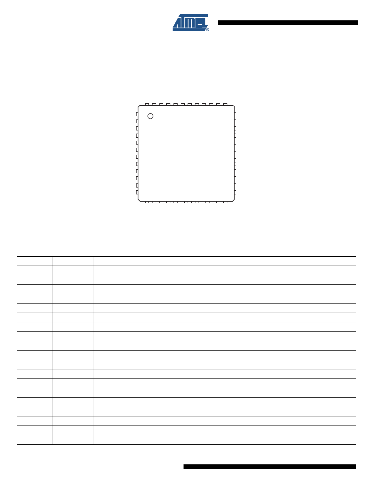
2. Pin Configuration
Figure 2-1. Pinning QFN48
AMIN1
AMIN2
AMCVC
AMPIND
SW1
FMPIND
FMIN1
FMIN12
FMIN2
DAC1
DAC2
SW2
AMOUT1
AMOUT2
AMAGCTC1
FMOUT1
FMOUT2
VST
IFIN1
IFREF
IFIN2
VRT
48 47 46 45 44 43 42 41 40 39 38 37
1
2
3
4
5
6
7
8
9
10
11
12
13 14 15 16 17 18 19 20 21 22 23 24
FMAGCTC
ATR4262M1
KAGC
IFGCL
IFGCM
SCL
SDA
ENABLE
AFCC
VRVCO
VCOB
IFIN3
AMAGCT2
36
35
34
33
32
31
30
29
28
27
26
25
VCOE
GNDVCO
SW3
IFOUT1
IFOUT2
VSPLL
REF1
REF2
VRPLL
AMLF
FMLF
VTUNE
GNDPLL
VCOBUF
Table 2-1. Pin Description
Pin Symbol Function
1 AMIN1 AM mixer input
2 AMIN2 AM mixer input
3 AMCVC AM cascode voltage output
4 AMPIND AM pin diode output
5 SW1 SW1 switching output
6 FMPIND FM pin diode output
7 FMIN1 FM mixer input 1
8 FMIN12 FM mixer input 12
9 FMIN2 FM mixer input 2
10 DAC1 DAC tuning voltage output 1
11 DAC2 DAC tuning voltage output 2
12 SW2 SW2 switching output/external tuning voltage input
13 FMAGCTC RF AGC FM time constant
14 KAGC Keyed AGC input/SW7/lock detect/AFSAMPLE
15 IFGCL IF gain control LSB/SW4
16 IFGCM IF gain control MSB/SW5
17 ENABLE Control bus ENABLE/address select
18 SDA Two-wire control bus SDA
19 SCL Two-wire control bus SCL
2
ATR4262M1 [Preliminary]
4994BS–AUDR–05/08
Page 3

Table 2-1. Pin Description
Pin Symbol Function
20 AFCC AFC control input/SW6 switching output/lock detect/AFHOLD
21 VRVCO Reference voltage VCO
22 VCOB VCO resonator (base)
23 VCOE VCO resonator (emitter)
24 GNDVCO VCO ground
25 VCOBUF VCO buffer output/input
26 GNDPLL PLL ground
27 VTUNE Tuning voltage output
28 FMLF PLL loopfilter FM
29 AMLF PLL loopfilter AM
30 VRPLL Reference voltage digital
31 REF2 RefClockInput2/crystal oscillator
32 REF1 RefClockInput1/crystal oscillator
33 VSPLL Supply voltage digital input
34 IFOUT2 IF output 2
35 IFOUT1 IF output 1
36 SW3 SW3 switching output/lock detect/AFSAMPLE
37 AMAGCTC2 RF AGC AM time constant 2
38 IFIN3 IF amplifier input
39 VRT Reference voltage tuner
40 IFIN2 IF amplifier input
41 IFREF IF reference voltage
42 IFIN1 IF amplifier input
43 VST Supply voltage tuner
44 FMOUT2 FM mixer output
45 FMOUT1 FM mixer output
46 AMAGCTC1 RF AGC AM time constant 1
47 AMOUT2 AM mixer output/FM Mixer Output 4
48 AMOUT1 AM mixer output/FM Mixer Output 3
Die pad GNDT_PAD Tuner RF and IF Ground
ATR4262M1 [Preliminary]
4994BS–AUDR–05/08
3
Page 4
3. Absolute Maximum Ratings
Stresses beyond those listed under “Absolute Maximum Ratings” may cause permanent damage to the device. This is a stress rating
only and functional operation of the device at these or any other conditions beyond those indicated in the operational sections of this
specification is not implied. Exposure to absolute maximum rating conditions for extended periods may affect device reliability.
Parameters Pin Group Min. Max. Unit
Digital –0.5 +5.5 V
Supply –0.5 +12 V
Voltage references –0.5 +6.4 V
Voltage
Current Switches 0 2.7 mA
Ambient temperature T
Storage temperature T
Junction temperature T
Power dissipation P
ESD HBM All pins –2 +2 kV
ESD MM All pins –200 +200 V
SW1, SW3 –0.5 +12 V
SW2 –0.5 V
+ 0.5 V
S
SW4, SW5, SW6, SW7 –0.5 + 5.5 V
Mixer outputs –0.5 +16 V
Analog –0.5 V
amb
stg
j
1.4 W
tot
–40 +100 °C
–40 +100 °C
+ 0.5 V
S
+150 °C
4. Thermal Resistance
Parameters Test Condition Symbol Value Unit
Thermal resistance junction-ambient Soldered to PCB R
thJA
30 K/W
5. Operating Range
Parameters Symbol Value Unit
Supply voltage V
Supply voltage for operation of control bus
(data preservation in bus registers is guaranteed)
Ambient temperature T
V
amb
S
S
8 to 10 V
7 to 10 V
–40 to +90 °C
4
ATR4262M1 [Preliminary]
4994BS–AUDR–05/08
Page 5

6. Functional Description
The ATR4262M1 front end is designed for world-tuner applications. Due to its flexible divider
arrangement, the tuner can be used for reception from 100 kHz to 163 MHz. The field of use
covers all the common radio broadcast services from AM-LW to AM-SW (up to 30 MHz) and
from FM-OIRT to US weatherband. The tuner application can be easily adapted to the requirements of DRM and HD-radio (IBOC).
• FM section
The ATR4262M1 contains a high performance FM image rejection mixer, which helps to
reduce the demands and the cost of the front end application. The FM mixer output can be
switched to an alternative pair of pins to allow different IF filter concepts for FM mode. Two
selectable inputs can be used for independent FM front end sections.
• AM section
The AM section contains a dedicated AM prescaler for the LO signal. Very small tuning
steps are possible using this divider, while at the same time a high PLL comparison frequency guarantees excellent phasenoise behavior.
•RF-AGC
Both AM and FM signal paths have their own RFAGCs with a wideband and a inband detec-
tor with individual thresholds. The thresholds for AM and FM can be programmed in 2 dB
steps. An optional keyed AGC function reduces the wideband AGC threshold up to 6 dB in
order to avoid desensitization of the tuner. Pin diode drivers for AM and FM are integrated to
reduce cost for external components. In addition to the pin diode control, a cascode control
voltage for the external LNA is provided by the AM-AGC block.
ATR4262M1 [Preliminary]
•IF stage
The IF amplifier has three selectable inputs, which can be matched to any common IF filter
impedance by external components. With these inputs, the tuner application can be easily
adapted to different broadcast standards, while conventional standards are still possible.
Gain can be set via pins or by setting bits, which makes the ATR4262M1 very versatile and
easy to adapt to different baseband architectures.
• Fractional PLL
The ATR4262M1 contains a complete fractional PLL, which guarantees fast lock time, low
phase noise and small tuning steps. A reference clock frequency from 9 kHz up to 21 MHz
provided by, for example, baseband can be used. Alternatively the integrated XCO with
standard crystals from 10 MHz to 21 MHz can be used as the reference for the PLL.
• Double tuner concept
Like phase diversity or background tuning, double-tuner applications are also possible. For
phase diversity applications, the tuner can also operate in slave mode with a master tuner
providing the VCO frequency for both tuners.
• Digital electronic alignment
Two independent gain and offset programmable DACs are available to tune the FM front
end section. The PLL’s tuning voltage is used as input for the DACs to ensure proper tracking to the reception frequency. In slave mode, the tuning voltage of a master tuner must be
applied to a dedicated input pin.
4994BS–AUDR–05/08
5
Page 6

• Alternative frequency check
An optional state machine can control the alternative frequency check sequence for some
common basebands. This feature reduces the CPU load of the main controller because the
statemachine outputs the signals with the correct timing for quality check and muting of the
baseband.
• Switching outputs
Up to seven general-purposes open-drain switches are available to simplify the customer
application.
• Two-wire control interface
The ATR4262 can be programmed via a fast-mode TWI bus interface. Two different IC
addresses can be selected to allow two tuners at the same bus segment. Various programming bits allow unique flexibility of operation modes. A tuner status byte provides
information about the receiving conditions and the PLL status.
• Package and power supply
The ATR4262 comes in a small outline QFN48 package to allow small and cost-effective
tuner applications. A single 8V to 10V supply voltage is sufficient to operate the ATR4262
and to reduce the complexity of the customer application.
6
ATR4262M1 [Preliminary]
4994BS–AUDR–05/08
Page 7

ATR4262M1 [Preliminary]
7. VCO and AM Prescaler Settings
Table 7-1 gives an example of the VCO divider and AM Prescaler settings and the reception
frequencies.
Table 7-1. Typical VCO Divider, AM Prescaler Settings, and Reception Frequencies
VCO-
divider
Band
FM 2 2 +10.7 87.5 108 196.4 237.4 -
JPN 3 3 –10.7 76 90 195.9 237.9 -
WB 1 2 +10.7 162.4 162.55 173.1 173.25 OIRT 3 3 +10.7 65.8 74 229.5 254.1 OIRT 3 3 –10.7 65.8 74 165.3 189.9 -
LW/MW - 2 +10.7 0.15 1.605 217 246.1 10
LW/MW - 2 +10.7 0.15 1.605 195.3 221.49 9
120m - 2 +10.7 2.3 2.5 208 211.2 8
...
49m - 2 +10.7 5.95 6.2 199.8 202.8 6
41m - 2 +10.7 7.1 7.35 213.6 216.6 6
31m - 2 +10.7 9.5 9.9 202 206 5
...
15m - 2 +10.7 21.45 21.85 192.9 195.3 3
(DFM)
N-div.
Prescaler
(D
) IF [MHz]
PLL
Min. Reception
Frequency [MHz]
Max. Reception
Frequency [MHz]
Min. VCO
Frequency
Max. VCO
Frequency
AM-
Prescaler
(DAM)
8. Power Supply
A small VCO frequency range of e.g., 195.3 MHz to 237.9 MHz allows reception of the most
important bands like FM, JPN, LW, MW, 49m, 41m, and 31m.
There is only one power supply voltage (8V to 10V) necessary for operation of the ATR4262M1.
4994BS–AUDR–05/08
7
Page 8

9. IF Filter Stage Concept
Ω
There are several different IF filter concepts possible depending on the broadcast standard and
the targeted quality range of the tuner. For that purpose a programmable switch for the FM mixer
output as well as three programmable inputs for the IF amplifier is available.
Table 9-1. IF Filter Stage Configuration
Configuration FMOUT AMFMOUT
AM low cost
AM ceramic filter
(compatible to DRM)
AM crystal filter
AM crystal filter, separate
tank
HD Radio
HD Radio low cost
HD Radio with AM filter
Not used or connected to
AMFMOUT
Mixer tank
Ceramic filter (BW 180 kHz)
Not used or connected to
AMFMOUT
Mixer tank
Ceramic filter (BW 180 kHz)
Mixer tank
Ceramic filter (BW 400 kHz)
Not used or connected to
AMFMOUT
Mixer tank
Ceramic filter (BW 400 kHz)
Ceramic filter (BW 180 kHz)
Ceramic filter (20 kHz)
Ceramic filter (BW 180 kHz)
Crystal filter (BW 7 kHz)
Crystal filter (BW 7 kHz)
Ceramic filter (BW 180 kHz)
Ceramic filter (BW 400 kHz)
Ceramic filter (BW 180 kHz)
Ceramic filter (BW 30 kHz)
Mixer tank
Mixer tank
Mixer tank
Mixer tank
Mixer tank
Mixer tank
Mixer tank
Number of Mixer
Output Tanks
11
22
12
22
22
11
23
Number of IF
Filters
Figure 9-1. Example of Simple IF Filter Stage Concept
RS2
180
+VS
F2
CF2in
MXFMOUT
RF12
RF1out y
x
RS1
1k8
CIF2in CIF1in
IFINFM
Rin(IF2) Rin(IF1)
KF2
RKF2out
330
KF1
RKF1out
1k8
IFINAM
x + y = 300
C
IFREF
8
ATR4262M1 [Preliminary]
4994BS–AUDR–05/08
Page 9

10. Double Tuner Application
Figure 10-1. Double Tuner Operation
ATR4262M1 [Preliminary]
IFOUT1 IFOUT2
270 pF*
1 µH*
3435
IFOUT1 IFOUT2
REF1
ATR4262M1
REF2
VCOBUF
VTUNE
or DAC
Master Slave
ENABLE ENABLE
17
10 nF
32
31 31
25
27 or
10,11
18
SDA
19
SCL
REF
CLK1
10 nF*
10 nF*
100 pF
REF
CLK2
32
25
12
18
19
REF1
REF2
VCOBUF
SW2
SDA
SCL
IFOUT1 IFOUT2
270 pF*
1 µH*
3435
IFOUT1 IFOUT2
ATR4262M1
17
5V
(high)
ENABLE1
SDA
10.1 Two-Wire Interface-Bus Address Modes
To allow programming of both ICs (e.g., double tuner), SCL and SDA can be connected to both
ICs.
There are two different modes for ENABLE. For example, the ENABLE pin of the master IC is
not connected (open mode). Only a capacitor to ground is required to avoid oscillations of the
ENABLE pin. To program the master IC for open mode, the address byte C2h must be used.
The ENABLE pin of the other IC (slave) has to be set to high. The applied voltage for high mode
should be in the range of 2.5V to 5.3V. Address byte C0h is used as the slave in this case.
Another possibility is the use of separate ENABLE lines which can be controlled by a
microcontroller.
SCL
ENABLE2
*) optional
4994BS–AUDR–05/08
9
Page 10

11. Ordering Information
Extended Type Number Package Remarks
ATR4262M1-PLQW QFN48 - 7 × 7 Taped and reeled
12. Package Information
Package: QFN 48 - 7 x 7
Exposed pad 4.5 x 4.5
(acc. JEDEC OUTLINE No. MO-220)
Dimensions in mm
Not indicated tolerances ± 0.05
7
48
1
12
Drawing-No.: 6.543-5089.01-4
Issue: 2; 24.01.03
1 max.
+0
0.05-0.05
0.23
0.4±0.1
36
25
5.5
4.5
4837
1
technical drawings
according to DIN
specifications
12
1324
0.5 nom.
10
ATR4262M1 [Preliminary]
4994BS–AUDR–05/08
Page 11

13. Revision History
Please note that the following page numbers referred to in this section refer to the specific revision
mentioned, not to this document.
Revision No. History
4994BS-AUDR-03/08
ATR4262M1 [Preliminary]
• all pages: Part Number changed in ATR4262M1
• all pages: IBOC changed in HD Radio
• Page 1: Features changed
• Page 4: Table Absolute Maximum Ratings changed
• Page 5: narrowband replaced by inband
• Page 7: Last row changed
• Page 9: Heading 22.1 changed
• Page 10: Ordering Information changed
4994BS–AUDR–05/08
11
Page 12

Headquarters International
Atmel Corporation
2325 Orchard Parkway
San Jose, CA 95131
USA
Tel: 1(408) 441-0311
Fax: 1(408) 487-2600
Atmel Asia
Room 1219
Chinachem Golden Plaza
77 Mody Road Tsimshatsui
East Kowloon
Hong Kong
Tel: (852) 2721-9778
Fax: (852) 2722-1369
Product Contact
Web Site
www.atmel.com
Literature Requests
www.atmel.com/literature
Atmel Europe
Le Krebs
8, Rue Jean-Pierre Timbaud
BP 309
78054
Saint-Quentin-en-Yvelines Cedex
France
Tel: (33) 1-30-60-70-00
Fax: (33) 1-30-60-71-11
Technical Support
broadcast@atmel.com
Atmel Japan
9F, Tonetsu Shinkawa Bldg.
1-24-8 Shinkawa
Chuo-ku, Tokyo 104-0033
Japan
Tel: (81) 3-3523-3551
Fax: (81) 3-3523-7581
Sales Contact
www.atmel.com/contacts
Disclaimer: The information in this document is provided in connection with Atmel products. No license, express or implied, by estoppel or otherwise, to any
intellectual property right is granted by this document or in connection with the sale of Atmel products. EXCEPT AS SET FORTH IN ATMEL’S TERMS AND CONDI-
TIONS OF SALE LOCATED ON ATMEL’S WEB SITE, ATMEL ASSUMES NO LIABILITY WHATSOEVER AND DISCLAIMS ANY EXPRESS, IMPLIED OR STATUTORY
WARRANTY RELATING TO ITS PRODUCTS INCLUDING, BUT NOT LIMITED TO, THE IMPLIED WARRANTY OF MERCHANTABILITY, FITNESS FOR A PARTICULAR
PURPOSE, OR NON-INFRINGEMENT. IN NO EVENT SHALL ATMEL BE LIABLE FOR ANY DIRECT, INDIRECT, CONSEQUENTIAL, PUNITIVE, SPECIAL OR INCIDENTAL D AMAGES (INCLUDING, WITHOUT LIMITA TION, D AMA GES FOR LOSS OF PROFITS, B USINESS INTERR UPTI ON, OR LOSS OF INFORMATION) ARISING OUT OF
THE USE OR INABILITY TO USE THIS DOCUMENT, EVEN IF ATMEL HAS BEEN ADVISED OF THE POSSIBILITY OF SUCH DAMAGES. Atmel makes no
representations or warranties with respect to the accuracy or completeness of the contents of this document and reserves the right to make changes to specifications
and product descriptions at any time without notice. Atmel does not make any commitment to update the information contained herein. Unless specifically provided
otherwise, Atmel products are not suitable for, and shall not be used in, automotive applications. Atmel’s products are not intended, authorized, or warranted for use
as components in applications intended to support or sustain life.
© 2008 Atmel Corporation. All rights reserved. Atmel®, logo and combinations thereof, and others are registered trademarks or trademarks of
Atmel Corporation or its subsidiaries. Other terms and product names may be trademarks of others.
4994BS–AUDR–05/08
 Loading...