

Page 1

Features
• High Performance, Low Power AVR
• Advanced RISC Architecture
– 131 Powerful Instructions – Most Single Clock Cycle Execution
– 32 x 8 General Purpose Working Registers
– Fully Static Operation
– Up to 20 MIPS Throughput at 20 MHz
– On-chip 2-cycle Multiplier
• High Endurance Non-volatile Memory Segments
– 4/8/16/32K Bytes of In-System Self-Programmable Flash progam memory
(ATmega48PA/88PA/168PA/328P)
– 256/512/512/1K Bytes EEPROM (ATmega48PA/88PA/168PA/328P)
– 512/1K/1K/2K Bytes Internal SRAM (ATmega48PA/88PA/168PA/328P)
– Write/Erase Cycles: 10,000 Flash/100,000 EEPROM
– Data retention: 20 years at 85°C/100 years at 25°C
– Optional Boot Code Section with Independent Lock Bits
In-System Programming by On-chip Boot Program
True Read-While-Write Operation
– Programming Lock for Software Security
• Peripheral Features
– Two 8-bit Timer/Counters with Separate Prescaler and Compare Mode
– One 16-bit Timer/Counter with Separate Prescaler, Compare Mode, and Capture
Mode
– Real Time Counter with Separate Oscillator
– Six PWM Channels
– 8-channel 10-bit ADC in TQFP and QFN/MLF package
Temperature Measurement
– 6-channel 10-bit ADC in PDIP Package
Temperature Measurement
– Programmable Serial USART
– Master/Slave SPI Serial Interface
– Byte-oriented 2-wire Serial Interface (Philips I
– Programmable Watchdog Timer with Separate On-chip Oscillator
– On-chip Analog Comparator
– Interrupt and Wake-up on Pin Change
• Special Microcontroller Features
– Power-on Reset and Programmable Brown-out Detection
– Internal Calibrated Oscillator
– External and Internal Interrupt Sources
– Six Sleep Modes: Idle, ADC Noise Reduction, Power-save, Power-down, Standby,
and Extended Standby
• I/O and Packages
– 23 Programmable I/O Lines
– 28-pin PDIP, 32-lead TQFP, 28-pad QFN/MLF and 32-pad QFN/MLF
• Operating Voltage:
– 1.8 - 5.5V for ATmega48PA/88PA/168PA/328P
• Temperature Range:
°C to 85°C
–-40
• Speed Grade:
– 0 - 20 MHz @ 1.8 - 5.5V
• Low Power Consumption at 1 MHz, 1.8V, 25°C for ATmega48PA/88PA/168PA/328P:
– Active Mode: 0.2 mA
– Power-down Mode: 0.1 µA
– Power-save Mode: 0.75 µA (Including 32 kHz RTC)
®
8-Bit Microcontroller
2
C compatible)
(1)
8-bit
Microcontroller
with 4/8/16/32K
Bytes In-System
Programmable
Flash
ATmega48PA
ATmega88PA
ATmega168PA
ATmega328P
Summary
Rev. 8161DS–AVR–10/09
Page 2
1. Pin Configurations
1
2
3
4
5
6
7
8
24
23
22
21
20
19
18
17
(PCINT19/OC2B/INT1) PD3
(PCINT20/XCK/T0) PD4
GND
VCC
GND
VCC
(PCINT6/XTAL1/TOSC1) PB6
(PCINT7/XTAL2/TOSC2) PB7
PC1 (ADC1/PCINT9)
PC0 (ADC0/PCINT8)
ADC7
GND
AREF
ADC6
AVC C
PB5 (SCK/PCINT5)
32313029282726
25
9101112131415
16
(PCINT21/OC0B/T1) PD5
(PCINT22/OC0A/AIN0) PD6
(PCINT23/AIN1) PD7
(PCINT0/CLKO/ICP1) PB0
(PCINT1/OC1A) PB1
(PCINT2/SS/OC1B) PB2
(PCINT3/OC2A/MOSI) PB3
(PCINT4/MISO) PB4
PD2 (INT0/PCINT18)
PD1 (TXD/PCINT17)
PD0 (RXD/PCINT16)
PC6 (RESET/PCINT14)
PC5 (ADC5/SCL/PCINT13)
PC4 (ADC4/SDA/PCINT12)
PC3 (ADC3/PCINT11)
PC2 (ADC2/PCINT10)
TQFP Top View
1
2
3
4
5
6
7
8
9
10
11
12
13
14
28
27
26
25
24
23
22
21
20
19
18
17
16
15
(PCINT14/RESET) PC6
(PCINT16/RXD) PD0
(PCINT17/TXD) PD1
(PCINT18/INT0) PD2
(PCINT19/OC2B/INT1) PD3
(PCINT20/XCK/T0) PD4
VCC
GND
(PCINT6/XTAL1/TOSC1) PB6
(PCINT7/XTAL2/TOSC2) PB7
(PCINT21/OC0B/T1) PD5
(PCINT22/OC0A/AIN0) PD6
(PCINT23/AIN1) PD7
(PCINT0/CLKO/ICP1) PB0
PC5 (ADC5/SCL/PCINT13)
PC4 (ADC4/SDA/PCINT12)
PC3 (ADC3/PCINT11)
PC2 (ADC2/PCINT10)
PC1 (ADC1/PCINT9)
PC0 (ADC0/PCINT8)
GND
AREF
AVCC
PB5 (SCK/PCINT5)
PB4 (MISO/PCINT4)
PB3 (MOSI/OC2A/PCINT3)
PB2 (SS/OC1B/PCINT2)
PB1 (OC1A/PCINT1)
PDIP
1
2
3
4
5
6
7
8
24
23
22
21
20
19
18
17
32313029282726
25
9101112131415
16
32 MLF Top View
(PCINT19/OC2B/INT1) PD3
(PCINT20/XCK/T0) PD4
GND
VCC
GND
VCC
(PCINT6/XTAL1/TOSC1) PB6
(PCINT7/XTAL2/TOSC2) PB7
PC1 (ADC1/PCINT9)
PC0 (ADC0/PCINT8)
ADC7
GND
AREF
ADC6
AVC C
PB5 (SCK/PCINT5)
(PCINT21/OC0B/T1) PD5
(PCINT23/AIN1) PD7
(PCINT0/CLKO/ICP1) PB0
(PCINT1/OC1A) PB1
(PCINT2/SS/OC1B) PB2
(PCINT3/OC2A/MOSI) PB3
(PCINT4/MISO) PB4
PD2 (INT0/PCINT18)
PD1 (TXD/PCINT17)
PD0 (RXD/PCINT16)
PC6 (RESET/PCINT14)
PC5 (ADC5/SCL/PCINT13)
PC4 (ADC4/SDA/PCINT12)
PC3 (ADC3/PCINT11)
PC2 (ADC2/PCINT10)
NOTE: Bottom pad should be soldered to ground.
1
2
3
4
5
6
7
21
20
19
18
17
16
15
28272625242322
891011121314
28 MLF Top View
(PCINT19/OC2B/INT1) PD3
(PCINT20/XCK/T0) PD4
VCC
GND
(PCINT6/XTAL1/TOSC1) PB6
(PCINT7/XTAL2/TOSC2) PB7
(PCINT21/OC0B/T1) PD5
(PCINT22/OC0A/AIN0) PD6
(PCINT23/AIN1) PD7
(PCINT0/CLKO/ICP1) PB0
(PCINT1/OC1A) PB1
(PCINT2/SS/OC1B) PB2
(PCINT3/OC2A/MOSI) PB3
(PCINT4/MISO) PB4
PD2 (INT0/PCINT18)
PD1 (TXD/PCINT17)
PD0 (RXD/PCINT16)
PC6 (RESET/PCINT14)
PC5 (ADC5/SCL/PCINT13)
PC4 (ADC4/SDA/PCINT12)
PC3 (ADC3/PCINT11)
PC2 (ADC2/PCINT10)
PC1 (ADC1/PCINT9)
PC0 (ADC0/PCINT8)
GND
AREF
AVCC
PB5 (SCK/PCINT5)
NOTE: Bottom pad should be soldered to ground.
Figure 1-1. Pinout ATmega48PA/88PA/168PA/328P
ATmega48PA/88PA/168PA/328P
8161DS–AVR–10/09
2
Page 3

1.1 Pin Descriptions
1.1.1 VCC
Digital supply voltage.
1.1.2 GND
Ground.
1.1.3 Port B (PB7:0) XTAL1/XTAL2/TOSC1/TOSC2
Port B is an 8-bit bi-directional I/O port with internal pull-up resistors (selected for each bit). The
Port B output buffers have symmetrical drive characteristics with both high sink and source
capability. As inputs, Port B pins that are externally pulled low will source current if the pull-up
resistors are activated. The Port B pins are tri-stated when a reset condition becomes active,
even if the clock is not running.
Depending on the clock selection fuse settings, PB6 can be used as input to the inverting Oscillator amplifier and input to the internal clock operating circuit.
Depending on the clock selection fuse settings, PB7 can be used as output from the inverting
Oscillator amplifier.
ATmega48PA/88PA/168PA/328P
1.1.4 Port C (PC5:0)
1.1.5 PC6/RESET
If the Internal Calibrated RC Oscillator is used as chip clock source, PB7..6 is used as TOSC2..1
input for the Asynchronous Timer/Counter2 if the AS2 bit in ASSR is set.
The various special features of Port B are elaborated in ”Alternate Functions of Port B” on page
76 and ”System Clock and Clock Options” on page 26.
Port C is a 7-bit bi-directional I/O port with internal pull-up resistors (selected for each bit). The
PC5..0 output buffers have symmetrical drive characteristics with both high sink and source
capability. As inputs, Port C pins that are externally pulled low will source current if the pull-up
resistors are activated. The Port C pins are tri-stated when a reset condition becomes active,
even if the clock is not running.
If the RSTDISBL Fuse is programmed, PC6 is used as an I/O pin. Note that the electrical characteristics of PC6 differ from those of the other pins of Port C.
If the RSTDISBL Fuse is unprogrammed, PC6 is used as a Reset input. A low level on this pin
for longer than the minimum pulse length will generate a Reset, even if the clock is not running.
The minimum pulse length is given in Table 28-3 on page 308. Shorter pulses are not guaranteed to generate a Reset.
The various special features of Port C are elaborated in ”Alternate Functions of Port C” on page
79.
1.1.6 Port D (PD7:0)
8161DS–AVR–10/09
Port D is an 8-bit bi-directional I/O port with internal pull-up resistors (selected for each bit). The
Port D output buffers have symmetrical drive characteristics with both high sink and source
capability. As inputs, Port D pins that are externally pulled low will source current if the pull-up
resistors are activated. The Port D pins are tri-stated when a reset condition becomes active,
even if the clock is not running.
3
Page 4

ATmega48PA/88PA/168PA/328P
The various special features of Port D are elaborated in ”Alternate Functions of Port D” on page
82.
1.1.7 AV
CC
AVCC is the supply voltage pin for the A/D Converter, PC3:0, and ADC7:6. It should be externally
connected to V
, even if the ADC is not used. If the ADC is used, it should be connected to V
CC
through a low-pass filter. Note that PC6..4 use digital supply voltage, VCC.
1.1.8 AREF
AREF is the analog reference pin for the A/D Converter.
1.1.9 ADC7:6 (TQFP and QFN/MLF Package Only)
In the TQFP and QFN/MLF package, ADC7:6 serve as analog inputs to the A/D converter.
These pins are powered from the analog supply and serve as 10-bit ADC channels.
CC
8161DS–AVR–10/09
4
Page 5
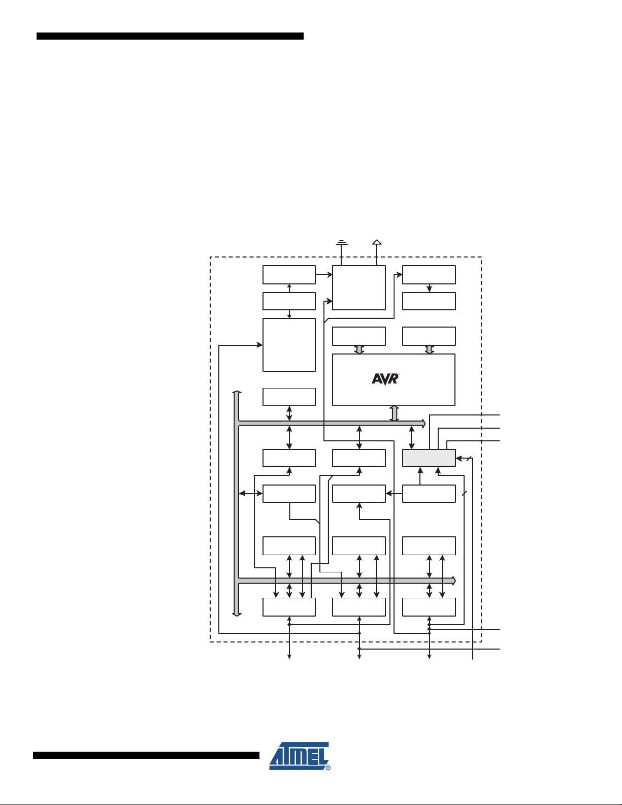
2. Overview
2.1 Block Diagram
ATmega48PA/88PA/168PA/328P
The ATmega48PA/88PA/168PA/328P is a low-power CMOS 8-bit microcontroller based on the
AVR enhanced RISC architecture. By executing powerful instructions in a single clock cycle, the
ATmega48PA/88PA/168PA/328P achieves throughputs approaching 1 MIPS per MHz allowing
the system designer to optimize power consumption versus processing speed.
Figure 2-1. Block Diagram
Powe r
RESET
Comp.
VCC
debugWIRE
PROGRAM
CPU
Internal
Bandgap
LOGIC
SRAMFlash
AVC C
AREF
GND
2
6
GND
Watchdog
Timer
Watchdog
Oscillator
Oscillator
Circuits /
Clock
Generation
EEPROM
8bit T/C 2
DATA B US
Supervision
POR / BOD &
16bit T/C 18bit T/C 0 A/D Conv.
Analog
8161DS–AVR–10/09
USART 0
SPI TWI
PORT C (7)PORT B (8)PORT D (8)
RESET
XTAL[1..2]
ADC[6..7]PC[0..6]PB[0..7]PD[0..7]
The AVR core combines a rich instruction set with 32 general purpose working registers. All the
32 registers are directly connected to the Arithmetic Logic Unit (ALU), allowing two independent
registers to be accessed in one single instruction executed in one clock cycle. The resulting
5
Page 6
ATmega48PA/88PA/168PA/328P
architecture is more code efficient while achieving throughputs up to ten times faster than conventional CISC microcontrollers.
The ATmega48PA/88PA/168PA/328P provides the following features: 4/8/16/32K bytes of InSystem Programmable Flash with Read-While-Write capabilities, 256/512/512/1K bytes
EEPROM, 512/1K/1K/2K bytes SRAM, 23 general purpose I/O lines, 32 general purpose working registers, three flexible Timer/Counters with compare modes, internal and external
interrupts, a serial programmable USART, a byte-oriented 2-wire Serial Interface, an SPI serial
port, a 6-channel 10-bit ADC (8 channels in TQFP and QFN/MLF packages), a programmable
Watchdog Timer with internal Oscillator, and five software selectable power saving modes. The
Idle mode stops the CPU while allowing the SRAM, Timer/Counters, USART, 2-wire Serial Interface, SPI port, and interrupt system to continue functioning. The Power-down mode saves the
register contents but freezes the Oscillator, disabling all other chip functions until the next interrupt or hardware reset. In Power-save mode, the asynchronous timer continues to run, allowing
the user to maintain a timer base while the rest of the device is sleeping. The ADC Noise Reduction mode stops the CPU and all I/O modules except asynchronous timer and ADC, to minimize
switching noise during ADC conversions. In Standby mode, the crystal/resonator Oscillator is
running while the rest of the device is sleeping. This allows very fast start-up combined with low
power consumption.
The device is manufactured using Atmel’s high density non-volatile memory technology. The
On-chip ISP Flash allows the program memory to be reprogrammed In-System through an SPI
serial interface, by a conventional non-volatile memory programmer, or by an On-chip Boot program running on the AVR core. The Boot program can use any interface to download the
application program in the Application Flash memory. Software in the Boot Flash section will
continue to run while the Application Flash section is updated, providing true Read-While-Write
operation. By combining an 8-bit RISC CPU with In-System Self-Programmable Flash on a
monolithic chip, the Atmel ATmega48PA/88PA/168PA/328P is a powerful microcontroller that
provides a highly flexible and cost effective solution to many embedded control applications.
The ATmega48PA/88PA/168PA/328P AVR is supported with a full suite of program and system
development tools including: C Compilers, Macro Assemblers, Program Debugger/Simulators,
In-Circuit Emulators, and Evaluation kits.
2.2 Comparison Between ATmega48PA, ATmega88PA, ATmega168PA and ATmega328P
The ATmega48PA, ATmega88PA, ATmega168PA and ATmega328P differ only in memory
sizes, boot loader support, and interrupt vector sizes. Table 2-1 summarizes the different memory and interrupt vector sizes for the three devices.
Table 2-1. Memory Size Summary
Device Flash EEPROM RAM Interrupt Vector Size
ATmega48PA 4K Bytes 256 Bytes 512 Bytes 1 instruction word/vector
ATmega88PA 8K Bytes 512 Bytes 1K Bytes 1 instruction word/vector
ATmega168PA 16K Bytes 512 Bytes 1K Bytes 2 instruction words/vector
ATmega328P 32K Bytes 1K Bytes 2K Bytes 2 instruction words/vector
ATmega88PA, ATmega168PA and ATmega328P support a real Read-While-Write Self-Programming mechanism. There is a separate Boot Loader Section, and the SPM instruction can
only execute from there. In ATmega48PA, there is no Read-While-Write support and no separate Boot Loader Section. The SPM instruction can execute from the entire Flash.
8161DS–AVR–10/09
6
Page 7

3. Resources
4. Data Retention
ATmega48PA/88PA/168PA/328P
A comprehensive set of development tools, application notes and datasheets are available for
download on http://www.atmel.com/avr.
Note: 1.
Reliability Qualification results show that the projected data retention failure rate is much less
than 1 PPM over 20 years at 85°C or 100 years at 25°C.
8161DS–AVR–10/09
7
Page 8
ATmega48PA/88PA/168PA/328P
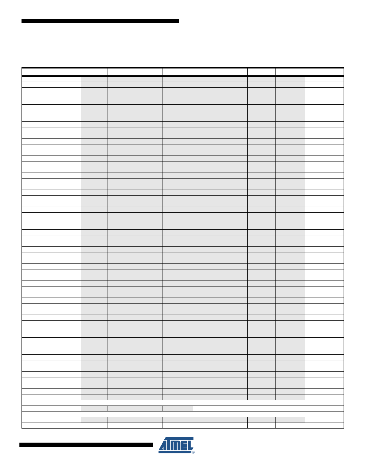
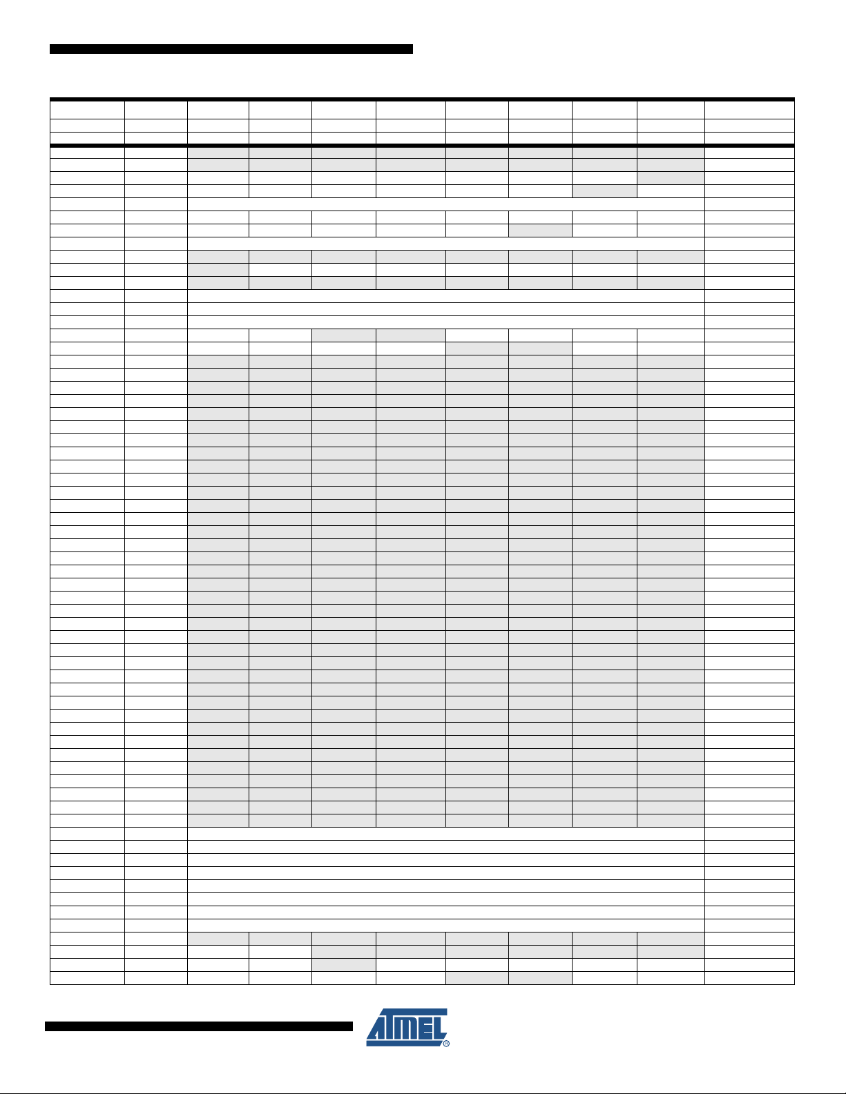
5. Register Summary
Address Name Bit 7 Bit 6 Bit 5 Bit 4 Bit 3 Bit 2 Bit 1 Bit 0 Page
(0xFF) Reserved – – – – – – – –
(0xFE) Reserved – – – – – – – –
(0xFD) Reserved – – – – – – – –
(0xFC) Reserved – – – – – – – –
(0xFB) Reserved – – – – – – – –
(0xFA) Reserved – – – – – – – –
(0xF9) Reserved – – – – – – – –
(0xF8) Reserved – – – – – – – –
(0xF7) Reserved – – – – – – – –
(0xF6) Reserved – – – – – – – –
(0xF5) Reserved – – – – – – – –
(0xF4) Reserved – – – – – – – –
(0xF3) Reserved
(0xF2) Reserved
(0xF1) Reserved – – – – – – – –
(0xF0) Reserved
(0xEF) Reserved
(0xEE) Reserved – – – – – – – –
(0xED) Reserved – – – – – – – –
(0xEC) Reserved – – – – – – – –
(0xEB) Reserved – – – – – – – –
(0xEA) Reserved – – – – – – – –
(0xE9) Reserved – – – – – – – –
(0xE8) Reserved – – – – – – – –
(0xE7) Reserved – – – – – – – –
(0xE6) Reserved – – – – – – – –
(0xE5) Reserved – – – – – – – –
(0xE4) Reserved – – – – – – – –
(0xE3) Reserved – – – – – – – –
(0xE2) Reserved – – – – – – – –
(0xE1) Reserved – – – – – – – –
(0xE0) Reserved – – – – – – – –
(0xDF) Reserved – – – – – – – –
(0xDE) Reserved – – – – – – – –
(0xDD) Reserved – – – – – – – –
(0xDC) Reserved – – – – – – – –
(0xDB) Reserved – – – – – – – –
(0xDA) Reserved – – – – – – – –
(0xD9) Reserved – – – – – – – –
(0xD8) Reserved
(0xD7) Reserved
(0xD6) Reserved – – – – – – – –
(0xD5) Reserved
(0xD4) Reserved
(0xD3) Reserved
(0xD2) Reserved – – – – – – – –
(0xD1) Reserved
(0xD0) Reserved
(0xCF) Reserved – – – – – – – –
(0xCE) Reserved
(0xCD) Reserved
(0xCC) Reserved – – – – – – – –
(0xCB) Reserved
(0xCA) Reserved
(0xC9) Reserved – – – – – – – –
(0xC8) Reserved
(0xC7) Reserved – – – – – – – –
(0xC6) UDR0 USART I/O Data Register 189
(0xC5) UBRR0H USART Baud Rate Register High 193
(0xC4) UBRR0L USART Baud Rate Register Low 193
(0xC3) Reserved
(0xC2) UCSR0C UMSEL01 UMSEL00 UPM01 UPM00 USBS0
– – – – – – – –
– – – – – – – –
– – – – – – – –
– – – – – – – –
– – – – – – – –
– – – – – – – –
– – – – – – – –
– – – – – – – –
– – – – – – – –
– – – – – – – –
– – – – – – – –
– – – – – – – –
– – – – – – – –
– – – – – – – –
– – – – – – – –
– – – – – – – –
– – – – – – – –
UCSZ01 /UDORD0 UCSZ00 / UCPHA0
UCPOL0 191/206
8161DS–AVR–10/09
8
Page 9
ATmega48PA/88PA/168PA/328P
Address Name Bit 7 Bit 6 Bit 5 Bit 4 Bit 3 Bit 2 Bit 1 Bit 0 Page
(0xC1) UCSR0B RXCIE0 TXCIE0 UDRIE0 RXEN0 TXEN0 UCSZ02 RXB80 TXB80 190
(0xC0) UCSR0A RXC0 TXC0 UDRE0 FE0 DOR0 UPE0 U2X0 MPCM0 189
(0xBF) Reserved – – – – – – – –
(0xBE) Reserved – – – – – – – –
(0xBD) TWAMR TWAM6 TWAM5 TWAM4 TWAM3 TWAM2 TWAM1 TWAM0 –239
(0xBC) TWCR TWINT TWEA TWSTA TWSTO TWWC TWEN –TWIE 236
(0xBB) TWDR 2-wire Serial Interface Data Register 238
(0xBA) TWAR TWA6 TWA5 TWA4 TWA3 TWA2 TWA1 TWA0 TWGCE 239
(0xB9) TWSR TWS7 TWS6 TWS5 TWS4 TWS3 –TWPS1TWPS0 238
(0xB8) TWBR 2-wire Serial Interface Bit Rate Register 236
(0xB7) Reserved – – – – – – –
(0xB6) ASSR – EXCLK AS2 TCN2UB OCR2AUB OCR2BUB TCR2AUB TCR2BUB 158
(0xB5) Reserved – – – – – – – –
(0xB4) OCR2B Timer/Counter2 Output Compare Register B 156
(0xB3) OCR2A Timer/Counter2 Output Compare Register A 156
(0xB2) TCNT2 Timer/Counter2 (8-bit) 156
(0xB1) TCCR2B FOC2A FOC2B
(0xB0) TCCR2A COM2A1 COM2A0 COM2B1 COM2B0
(0xAF) Reserved – – – – – – – –
(0xAE) Reserved
(0xAD) Reserved
(0xAC) Reserved – – – – – – – –
(0xAB) Reserved – – – – – – – –
(0xAA) Reserved – – – – – – – –
(0xA9) Reserved – – – – – – – –
(0xA8) Reserved – – – – – – – –
(0xA7) Reserved – – – – – – – –
(0xA6) Reserved – – – – – – – –
(0xA5) Reserved – – – – – – – –
(0xA4) Reserved – – – – – – – –
(0xA3) Reserved – – – – – – – –
(0xA2) Reserved – – – – – – – –
(0xA1) Reserved – – – – – – – –
(0xA0) Reserved – – – – – – – –
(0x9F) Reserved – – – – – – – –
(0x9E) Reserved – – – – – – – –
(0x9D) Reserved – – – – – – – –
(0x9C) Reserved – – – – – – – –
(0x9B) Reserved – – – – – – – –
(0x9A) Reserved – – – – – – – –
(0x99) Reserved – – – – – – – –
(0x98) Reserved – – – – – – – –
(0x97) Reserved – – – – – – – –
(0x96) Reserved
(0x95) Reserved
(0x94) Reserved – – – – – – – –
(0x93) Reserved
(0x92) Reserved
(0x91) Reserved
(0x90) Reserved – – – – – – – –
(0x8F) Reserved
(0x8E) Reserved
(0x8D) Reserved – – – – – – – –
(0x8C) Reserved
(0x8B) OCR1BH Timer/Counter1 - Output Compare Register B High Byte 132
(0x8A) OCR1BL Timer/Counter1 - Output Compare Register B Low Byte 132
(0x89) OCR1AH Timer/Counter1 - Output Compare Register A High Byte 132
(0x88) OCR1AL Timer/Counter1 - Output Compare Register A Low Byte 132
(0x87) ICR1H Timer/Counter1 - Input Capture Register High Byte 133
(0x86) ICR1L Timer/Counter1 - Input Capture Register Low Byte 133
(0x85) TCNT1H Timer/Counter1 - Counter Register High Byte 132
(0x84) TCNT1L Timer/Counter1 - Counter Register Low Byte 132
(0x83) Reserved – – – – – – – –
(0x82) TCCR1C FOC1A FOC1B – – – – – –131
(0x81) TCCR1B ICNC1 ICES1
(0x80) TCCR1A COM1A1 COM1A0 COM1B1 COM1B0
– – – – – – – –
– – – – – – – –
– – – – – – – –
– – – – – – – –
– – – – – – – –
– – – – – – – –
– – – – – – – –
– – – – – – – –
– – – – – – – –
– – – – – – – –
– – WGM22 CS22 CS21 CS20
– –WGM21WGM20 152
– WGM13 WGM12 CS12 CS11 CS10 130
– –WGM11WGM10 128
155
8161DS–AVR–10/09
9
Page 10

ATmega48PA/88PA/168PA/328P
Address Name Bit 7 Bit 6 Bit 5 Bit 4 Bit 3 Bit 2 Bit 1 Bit 0 Page
(0x7F) DIDR1 – – – – – –AIN1DAIN0D 244
(0x7E) DIDR0 – – ADC5D ADC4D ADC3D ADC2D ADC1D ADC0D 261
(0x7D) Reserved – – – – – – – –
(0x7C) ADMUX REFS1 REFS0 ADLAR – MUX3 MUX2 MUX1 MUX0 257
(0x7B) ADCSRB –ACME – – – ADTS2 ADTS1 ADTS0 260
(0x7A) ADCSRA ADEN ADSC ADATE ADIF ADIE ADPS2 ADPS1 ADPS0 258
(0x79) ADCH ADC Data Register High byte 260
(0x78) ADCL ADC Data Register Low byte 260
(0x77) Reserved – – – – – – – –
(0x76) Reserved – – – – – – – –
(0x75) Reserved – – – – – – – –
(0x74) Reserved – – – – – – – –
(0x73) Reserved – – – – – – – –
(0x72) Reserved – – – – – – – –
(0x71) Reserved – – – – – – – –
(0x70) TIMSK2 – – – – – OCIE2B OCIE2A TOIE2 157
(0x6F) TIMSK1
(0x6E) TIMSK0
(0x6D) PCMSK2 PCINT23 PCINT22 PCINT21 PCINT20 PCINT19 PCINT18 PCINT17 PCINT16 68
(0x6C) PCMSK1
(0x6B) PCMSK0 PCINT7 PCINT6 PCINT5 PCINT4 PCINT3 PCINT2 PCINT1 PCINT0 68
(0x6A) Reserved
(0x69) EICRA – – – –ISC11ISC10ISC01ISC00 65
(0x68) PCICR – – – – – PCIE2 PCIE1 PCIE0
(0x67) Reserved – – – – – – – –
(0x66) OSCCAL Oscillator Calibration Register 37
(0x65) Reserved – – – – – – – –
(0x64) PRR PRTWI PRTIM2 PRTIM0 – PRTIM1 PRSPI PRUSART0 PRADC 42
(0x63) Reserved – – – – – – – –
(0x62) Reserved – – – – – – – –
(0x61) CLKPR CLKPCE – – – CLKPS3 CLKPS2 CLKPS1 CLKPS0 37
(0x60) WDTCSR WDIF WDIE WDP3 WDCE WDE WDP2 WDP1 WDP0 54
0x3F (0x5F) SREG I T H S V N Z C 9
0x3E (0x5E) SPH – – – – – (SP10)
0x3D (0x5D) SPL SP7 SP6 SP5 SP4 SP3 SP2 SP1 SP0 12
0x3C (0x5C) Reserved – – – – – – – –
0x3B (0x5B) Reserved – – – – – – – –
0x3A (0x5A) Reserved – – – – – – – –
0x39 (0x59) Reserved – – – – – – – –
0x38 (0x58) Reserved – – – – – – – –
0x37 (0x57) SPMCSR SPMIE (RWWSB)
0x36 (0x56) Reserved – – – – – – – –
0x35 (0x55) MCUCR – BODS BODSE PUD – – IVSEL IVCE 44/62/86
0x34 (0x54) MCUSR
0x33 (0x53) SMCR
0x32 (0x52) Reserved – – – – – – – –
0x31 (0x51) Reserved
0x30 (0x50) ACSR ACD ACBG ACO ACI ACIE ACIC ACIS1 ACIS0 242
0x2F (0x4F) Reserved – – – – – – – –
0x2E (0x4E) SPDR SPI Data Register 169
0x2D (0x4D) SPSR SPIF WCOL
0x2C (0x4C) SPCR SPIE SPE DORD MSTR CPOL CPHA SPR1 SPR0 167
0x2B (0x4B) GPIOR2 General Purpose I/O Register 2 25
0x2A (0x4A) GPIOR1 General Purpose I/O Register 1 25
0x29 (0x49) Reserved
0x28 (0x48) OCR0B Timer/Counter0 Output Compare Register B
0x27 (0x47) OCR0A Timer/Counter0 Output Compare Register A
0x26 (0x46) TCNT0 Timer/Counter0 (8-bit)
0x25 (0x45) TCCR0B FOC0A FOC0B – – WGM02 CS02 CS01 CS00
0x24 (0x44) TCCR0A COM0A1 COM0A0 COM0B1 COM0B0
0x23 (0x43) GTCCR TSM – – – – – PSRASY PSRSYNC 137/159
0x22 (0x42) EEARH (EEPROM Address Register High Byte)
0x21 (0x41) EEARL EEPROM Address Register Low Byte 21
0x20 (0x40) EEDR EEPROM Data Register 21
0x1F (0x3F) EECR – – EEPM1 EEPM0 EERIE EEMPE EEPE EERE 21
0x1E (0x3E) GPIOR0 General Purpose I/O Register 0 25
– –ICIE1 – – OCIE1B OCIE1A TOIE1 133
– – – – – OCIE0B OCIE0A TOIE0 105
– PCINT14 PCINT13 PCINT12 PCINT11 PCINT10 PCINT9 PCINT8 68
– – – – – – – –
5.
5.
– – – – WDRF BORF EXTRF PORF 54
– – – –SM2SM1SM0SE 40
– – – – – – – –
– – – – – – – –
– (RWWSRE)
– – – – – SPI2X 168
5.
BLBSET PGWRT PGERS SELFPRGEN 284
– –WGM01WGM00
5.
SP9 SP8 12
21
8161DS–AVR–10/09
10
Page 11

ATmega48PA/88PA/168PA/328P
Address Name Bit 7 Bit 6 Bit 5 Bit 4 Bit 3 Bit 2 Bit 1 Bit 0 Page
0x1D (0x3D) EIMSK – – – – – –INT1INT0 66
0x1C (0x3C) EIFR – – – – – – INTF1 INTF0 66
0x1B (0x3B) PCIFR – – – – – PCIF2 PCIF1 PCIF0
0x1A (0x3A) Reserved – – – – – – – –
0x19 (0x39) Reserved – – – – – – – –
0x18 (0x38) Reserved – – – – – – – –
0x17 (0x37) TIFR2 – – – – – OCF2B OCF2A TOV2 157
0x16 (0x36) TIFR1 – –ICF1 – – OCF1B OCF1A TOV1 134
0x15 (0x35) TIFR0 – – – – – OCF0B OCF0A TOV0
0x14 (0x34) Reserved – – – – – – – –
0x13 (0x33) Reserved – – – – – – – –
0x12 (0x32) Reserved – – – – – – – –
0x11 (0x31) Reserved – – – – – – – –
0x10 (0x30) Reserved – – – – – – – –
0x0F (0x2F) Reserved – – – – – – – –
0x0E (0x2E) Reserved – – – – – – – –
0x0D (0x2D) Reserved
0x0C (0x2C) Reserved
0x0B (0x2B) PORTD PORTD7 PORTD6 PORTD5 PORTD4 PORTD3 PORTD2 PORTD1 PORTD0 87
0x0A (0x2A) DDRD DDD7 DDD6 DDD5 DDD4 DDD3 DDD2 DDD1 DDD0 87
0x09 (0x29) PIND PIND7 PIND6 PIND5 PIND4 PIND3 PIND2 PIND1 PIND0 87
0x08 (0x28) PORTC – PORTC6 PORTC5 PORTC4 PORTC3 PORTC2 PORTC1 PORTC0 86
0x07 (0x27) DDRC – DDC6 DDC5 DDC4 DDC3 DDC2 DDC1 DDC0 86
0x06 (0x26) PINC – PINC6 PINC5 PINC4 PINC3 PINC2 PINC1 PINC0 86
0x05 (0x25) PORTB PORTB7 PORTB6 PORTB5 PORTB4 PORTB3 PORTB2 PORTB1 PORTB0 86
0x04 (0x24) DDRB DDB7 DDB6 DDB5 DDB4 DDB3 DDB2 DDB1 DDB0 86
0x03 (0x23) PINB PINB7 PINB6 PINB5 PINB4 PINB3 PINB2 PINB1 PINB0 86
0x02 (0x22) Reserved – – – – – – – –
0x01 (0x21) Reserved – – – – – – – –
0x0 (0x20) Reserved – – – – – – – –
Note: 1. For compatibility with future devices, reserved bits should be written to zero if accessed. Reserved I/O memory addresses
should never be written.
2. I/O Registers within the address range 0x00 - 0x1F are directly bit-accessible using the SBI and CBI instructions. In these
registers, the value of single bits can be checked by using the SBIS and SBIC instructions.
3. Some of the Status Flags are cleared by writing a logical one to them. Note that, unlike most other AVRs, the CBI and SBI
instructions will only operate on the specified bit, and can therefore be used on registers containing such Status Flags. The
CBI and SBI instructions work with registers 0x00 to 0x1F only.
4. When using the I/O specific commands IN and OUT, the I/O addresses 0x00 - 0x3F must be used. When addressing I/O
Registers as data space using LD and ST instructions, 0x20 must be added to these addresses. The
ATmega48PA/88PA/168PA/328P is a complex microcontroller with more peripheral units than can be supported within the 64
location reserved in Opcode for the IN and OUT instructions. For the Extended I/O space from 0x60 - 0xFF in SRAM, only
the ST/STS/STD and LD/LDS/LDD instructions can be used.
5. Only valid for ATmega88PA.
– – – – – – – –
– – – – – – – –
8161DS–AVR–10/09
11
Page 12

ATmega48PA/88PA/168PA/328P
6. Instruction Set Summary
Mnemonics Operands Description Operation Flags #Clocks
ARITHMETIC AND LOGIC INSTRUCTIONS
ADD Rd, Rr Add two Registers Rd ← Rd + Rr Z,C,N,V,H 1
ADC Rd, Rr Add with Carry two Registers Rd ← Rd + Rr + C Z,C,N,V,H 1
ADIW Rdl,K Add Immediate to Word Rdh:Rdl ← Rdh:Rdl + K Z,C,N,V,S 2
SUB Rd, Rr Subtract two Registers Rd ← Rd - Rr Z,C,N,V,H 1
SUBI Rd, K Subtract Constant from Register Rd ← Rd - K Z,C,N,V,H 1
SBC Rd, Rr Subtract with Carry two Registers Rd ← Rd - Rr - C Z,C,N,V,H 1
SBCI Rd, K Subtract with Carry Constant from Reg. Rd ← Rd - K - C Z,C,N,V,H 1
SBIW Rdl,K Subtract Immediate from Word Rdh:Rdl ← Rdh:Rdl - K Z,C,N,V,S 2
AND Rd, Rr Logical AND Registers Rd ← Rd • Rr Z,N,V 1
ANDI Rd, K Logical AND Register and Constant Rd ← Rd • K Z,N,V 1
OR Rd, Rr Logical OR Registers Rd ← Rd v Rr Z,N,V 1
ORI Rd, K Logical OR Register and Constant Rd ← Rd v K Z,N,V 1
EOR Rd, Rr Exclusive OR Registers Rd ← Rd ⊕ Rr Z,N,V 1
COM Rd One’s Complement Rd ← 0xFF − Rd Z,C,N,V 1
NEG Rd Two’s Complement Rd ← 0x00 − Rd Z,C,N,V,H 1
SBR Rd,K Set Bit(s) in Register Rd ← Rd v K Z,N,V 1
CBR Rd,K Clear Bit(s) in Register Rd ← Rd • (0xFF - K) Z,N,V 1
INC Rd Increment Rd ← Rd + 1 Z,N,V 1
DEC Rd Decrement Rd ← Rd − 1 Z,N,V 1
TST Rd Test for Zero or Minus Rd ← Rd • Rd Z,N,V 1
CLR Rd Clear Register Rd ← Rd ⊕ Rd Z,N,V 1
SER Rd Set Register Rd ← 0xFF None 1
MUL Rd, Rr Multiply Unsigned R1:R0 ← Rd x Rr Z,C 2
MULS Rd, Rr Multiply Signed R1:R0 ← Rd x Rr Z,C 2
MULSU Rd, Rr Multiply Signed with Unsigned R1:R0 ← Rd x Rr Z,C 2
FMUL Rd, Rr Fractional Multiply Unsigned R1:R0 ← (Rd x Rr) << 1 Z,C 2
FMULS Rd, Rr Fractional Multiply Signed R1:R0 ← (Rd x Rr) << 1 Z,C 2
FMULSU Rd, Rr Fractional Multiply Signed with Unsigned R1:R0 ← (Rd x Rr) << 1 Z,C 2
BRANCH INSTRUCTIONS
RJMP k Relative Jump PC ← PC + k + 1 None 2
IJMP Indirect Jump to (Z) PC ← Z None 2
(1)
JMP
RCALL k Relative Subroutine Call PC ← PC + k + 1 None 3
ICALL Indirect Call to (Z) PC ← ZNone3
(1)
CALL
RET Subroutine Return PC ← STACK None 4
RETI Interrupt Return PC ← STACK I 4
CPSE Rd,Rr Compare, Skip if Equal if (Rd = Rr) PC ← PC + 2 or 3 None 1/2/3
CP Rd,Rr Compare Rd − Rr Z, N,V,C,H 1
CPC Rd,Rr Compare with Carry Rd − Rr − C Z, N,V,C,H 1
CPI Rd,K Compare Register with Immediate Rd − K Z, N,V,C,H 1
SBRC Rr, b Skip if Bit in Register Cleared if (Rr(b)=0) PC ← PC + 2 or 3 None 1/2/3
SBRS Rr, b Skip if Bit in Register is Set if (Rr(b)=1) PC ← PC + 2 or 3 None 1/2/3
SBIC P, b Skip if Bit in I/O Register Cleared if (P(b)=0) PC ← PC + 2 or 3 None 1/2/3
SBIS P, b Skip if Bit in I/O Register is Set if (P(b)=1) PC ← PC + 2 or 3 None 1/2/3
BRBS s, k Branch if Status Flag Set if (SREG(s) = 1) then PC←PC+k + 1 None 1/2
BRBC s, k Branch if Status Flag Cleared if (SREG(s) = 0) then PC ←PC+k + 1 None 1/2
BREQ k Branch if Equal if (Z = 1) then PC ← PC + k + 1 None 1/2
BRNE k Branch if Not Equal if (Z = 0) then PC ← PC + k + 1 None 1/2
BRCS k Branch if Carry Set if (C = 1) then PC ← PC + k + 1 None 1/2
BRCC k Branch if Carry Cleared if (C = 0) then PC ← PC + k + 1 None 1/2
BRSH k Branch if Same or Higher if (C = 0) then PC ← PC + k + 1 None 1/2
BRLO k Branch if Lower if (C = 1) then PC ← PC + k + 1 None 1/2
BRMI k Branch if Minus if (N = 1) then PC ← PC + k + 1 None 1/2
BRPL k Branch if Plus if (N = 0) then PC ← PC + k + 1 None 1/2
BRGE k Branch if Greater or Equal, Signed if (N ⊕ V= 0) then PC ← PC + k + 1 None 1/2
BRLT k Branch if Less Than Zero, Signed if (N ⊕ V= 1) then PC ← PC + k + 1 None 1/2
BRHS k Branch if Half Carry Flag Set if (H = 1) then PC ← PC + k + 1 None 1/2
BRHC k Branch if Half Carry Flag Cleared if (H = 0) then PC ← PC + k + 1 None 1/2
BRTS k Branch if T Flag Set if (T = 1) then PC ← PC + k + 1 None 1/2
BRTC k Branch if T Flag Cleared if (T = 0) then PC ← PC + k + 1 None 1/2
BRVS k Branch if Overflow Flag is Set if (V = 1) then PC ← PC + k + 1 None 1/2
BRVC k Branch if Overflow Flag is Cleared if (V = 0) then PC ← PC + k + 1 None 1/2
k Direct Jump PC ← kNone3
k Direct Subroutine Call PC ← kNone4
8161DS–AVR–10/09
12
Page 13

ATmega48PA/88PA/168PA/328P
Mnemonics Operands Description Operation Flags #Clocks
BRIE k Branch if Interrupt Enabled if ( I = 1) then PC ← PC + k + 1 None 1/2
BRID k Branch if Interrupt Disabled if ( I = 0) then PC ← PC + k + 1 None 1/2
BIT AND BIT-TEST INSTRUCTIONS
SBI P,b Set Bit in I/O Register I/O(P,b) ← 1None2
CBI P,b Clear Bit in I/O Register I/O(P,b) ← 0None2
LSL Rd Logical Shift Left Rd(n+1) ← Rd(n), Rd(0) ← 0 Z,C,N,V 1
LSR Rd Logical Shift Right Rd(n) ← Rd(n+1), Rd(7) ← 0 Z,C,N,V 1
ROL Rd Rotate Left Through Carry Rd(0)←C,Rd(n+1)← Rd(n),C←Rd(7) Z,C,N,V 1
ROR Rd Rotate Right Through Carry Rd(7)←C,Rd(n)← Rd(n+1),C←Rd(0) Z,C,N,V 1
ASR Rd Arithmetic Shift Right Rd(n) ← Rd(n+1), n=0..6 Z,C,N,V 1
SWAP Rd Swap Nibbles Rd(3..0)←Rd(7..4),Rd(7..4)←Rd(3..0) None 1
BSET s Flag Set SREG(s) ← 1 SREG(s) 1
BCLR s Flag Clear SREG(s) ← 0 SREG(s) 1
BST Rr, b Bit Store from Register to T T ← Rr(b) T 1
BLD Rd, b Bit load from T to Register Rd(b) ← TNone1
SEC Set Carry C ← 1C1
CLC Clear Carry C ← 0 C 1
SEN Set Negative Flag N ← 1N1
CLN Clear Negative Flag N ← 0 N 1
SEZ Set Zero Flag Z ← 1Z1
CLZ Clear Zero Flag Z ← 0 Z 1
SEI Global Interrupt Enable I ← 1I1
CLI Global Interrupt Disable I ← 0 I 1
SES Set Signed Test Flag S ← 1S1
CLS Clear Signed Test Flag S ← 0 S 1
SEV Set Twos Complement Overflow. V ← 1V1
CLV Clear Twos Complement Overflow V ← 0 V 1
SET Set T in SREG T ← 1T1
CLT Clear T in SREG T ← 0 T 1
SEH Set Half Carry Flag in SREG H ← 1H1
CLH Clear Half Carry Flag in SREG H ← 0 H 1
DATA TRANSFER INSTRUCTIONS
MOV Rd, Rr Move Between Registers Rd ← Rr None 1
MOVW Rd, Rr Copy Register Word
LDI Rd, K Load Immediate Rd ← KNone1
LD Rd, X Load Indirect Rd ← (X) None 2
LD Rd, X+ Load Indirect and Post-Inc. Rd ← (X), X ← X + 1 None 2
LD Rd, - X Load Indirect and Pre-Dec. X ← X - 1, Rd ← (X) None 2
LD Rd, Y Load Indirect Rd ← (Y) None 2
LD Rd, Y+ Load Indirect and Post-Inc. Rd ← (Y), Y ← Y + 1 None 2
LD Rd, - Y Load Indirect and Pre-Dec. Y ← Y - 1, Rd ← (Y) None 2
LDD Rd,Y+q Load Indirect with Displacement Rd ← (Y + q) None 2
LD Rd, Z Load Indirect Rd ← (Z) None 2
LD Rd, Z+ Load Indirect and Post-Inc. Rd ← (Z), Z ← Z+1 None 2
LD Rd, -Z Load Indirect and Pre-Dec. Z ← Z - 1, Rd ← (Z) None 2
LDD Rd, Z+q Load Indirect with Displacement Rd ← (Z + q) None 2
LDS Rd, k Load Direct from SRAM Rd ← (k) None 2
ST X, Rr Store Indirect (X) ← Rr None 2
ST X+, Rr Store Indirect and Post-Inc. (X) ← Rr, X ← X + 1 None 2
ST - X, Rr Store Indirect and Pre-Dec. X ← X - 1, (X) ← Rr None 2
ST Y, Rr Store Indirect (Y) ← Rr None 2
ST Y+, Rr Store Indirect and Post-Inc. (Y) ← Rr, Y ← Y + 1 None 2
ST - Y, Rr Store Indirect and Pre-Dec. Y ← Y - 1, (Y) ← Rr None 2
STD Y+q,Rr Store Indirect with Displacement (Y + q) ← Rr None 2
ST Z, Rr Store Indirect (Z) ← Rr None 2
ST Z+, Rr Store Indirect and Post-Inc. (Z) ← Rr, Z ←
ST -Z, Rr Store Indirect and Pre-Dec. Z ← Z - 1, (Z) ← Rr None 2
STD Z+q,Rr Store Indirect with Displacement (Z + q) ← Rr None 2
STS k, Rr Store Direct to SRAM (k) ← Rr None 2
LPM Load Program Memory R0 ← (Z) None 3
LPM Rd, Z Load Program Memory Rd ← (Z) None 3
LPM Rd, Z+ Load Program Memory and Post-Inc Rd ← (Z), Z ← Z+1 None 3
SPM Store Program Memory (Z) ← R1:R0 None -
IN Rd, P In Port Rd ← PNone1
OUT P, Rr Out Port P ← Rr None 1
PUSH Rr Push Register on Stack STACK ← Rr None 2
Rd+1:Rd ← Rr+1:Rr
Z + 1 None 2
None 1
8161DS–AVR–10/09
13
Page 14

ATmega48PA/88PA/168PA/328P
Mnemonics Operands Description Operation Flags #Clocks
POP Rd Pop Register from Stack Rd ← STACK None 2
MCU CONTROL INSTRUCTIONS
NOP No Operation None 1
SLEEP Sleep (see specific descr. for Sleep function) None 1
WDR Watchdog Reset (see specific descr. for WDR/timer) None 1
BREAK Break For On-chip Debug Only None N/A
8161DS–AVR–10/09
14
Page 15

7. Ordering Information
7.1 ATmega48PA
ATmega48PA/88PA/168PA/328P
Speed (MHz) Power Supply Ordering Code
ATmega48PA-AU
(3)
20
Note: 1. This device can also be supplied in wafer form. Please contact your local Atmel sales office for detailed ordering information
and minimum quantities.
2. Pb-free packaging complies to the European Directive for Restriction of Hazardous Substances (RoHS directive).Also
Halide free and fully Green.
3. See ”Speed Grades” on page 306.
4. NiPdAu Lead Finish.
1.8 - 5.5
ATmega48PA-MMH
ATmega48PA-MU
ATmega48PA-PU
(2)
(4)
Package
32A
28M1
32M1-A
28P3
(1)
Operational Range
Industrial
°C to 85°C)
(-40
Package Type
32A 32-lead, Thin (1.0 mm) Plastic Quad Flat Package (TQFP)
28M1 28-pad, 4 x 4 x 1.0 body, Lead Pitch 0.45 mm Quad Flat No-Lead/Micro Lead Frame Package (QFN/MLF)
32M1-A 32-pad, 5 x 5 x 1.0 body, Lead Pitch 0.50 mm Quad Flat No-Lead/Micro Lead Frame Package (QFN/MLF)
28P3 28-lead, 0.300” Wide, Plastic Dual Inline Package (PDIP)
8161DS–AVR–10/09
15
Page 16

7.2 ATmega88PA
ATmega48PA/88PA/168PA/328P
Speed (MHz) Power Supply Ordering Code
ATmega88PA-AU
20
(3)
1.8 - 5.5
ATmega88PA-MMH
ATmega88PA-MU
ATmega88PA-PU
(2)
Package
32A
(4)
28M1
32M1-A
28P3
(1)
Operational Range
Industrial
°C to 85°C)
(-40
Note: 1. This device can also be supplied in wafer form. Please contact your local Atmel sales office for detailed ordering information
and minimum quantities.
2. Pb-free packaging complies to the European Directive for Restriction of Hazardous Substances (RoHS directive).Also
Halide free and fully Green.
3. See ”Speed Grades” on page 306.
4. NiPdAu Lead Finish.
Package Type
32A 32-lead, Thin (1.0 mm) Plastic Quad Flat Package (TQFP)
28M1 28-pad, 4 x 4 x 1.0 body, Lead Pitch 0.45 mm Quad Flat No-Lead/Micro Lead Frame Package (QFN/MLF)
32M1-A 32-pad, 5 x 5 x 1.0 body, Lead Pitch 0.50 mm Quad Flat No-Lead/Micro Lead Frame Package (QFN/MLF)
28P3 28-lead, 0.300” Wide, Plastic Dual Inline Package (PDIP)
8161DS–AVR–10/09
16
Page 17

7.3 ATmega168PA
ATmega48PA/88PA/168PA/328P
Speed (MHz)
(3)
20 1.8 - 5.5
Power Supply Ordering Code
ATmega168PA-AU
ATmega168PA-MMH
ATmega168PA-MU
ATmega168PA-PU
(2)
Package
(1)
Operational Range
32A
(4)
28M1
32M1-A
Industrial
°C to 85°C)
(-40
28P3
Note: 1. This device can also be supplied in wafer form. Please contact your local Atmel sales office for detailed ordering information
and minimum quantities.
2. Pb-free packaging complies to the European Directive for Restriction of Hazardous Substances (RoHS directive).Also
Halide free and fully Green.
3. See ”Speed Grades” on page 312.
4. NiPdAu Lead Finish.
Package Type
32A 32-lead, Thin (1.0 mm) Plastic Quad Flat Package (TQFP)
28M1 28-pad, 4 x 4 x 1.0 body, Lead Pitch 0.45 mm Quad Flat No-Lead/Micro Lead Frame Package (QFN/MLF)
32M1-A 32-pad, 5 x 5 x 1.0 body, Lead Pitch 0.50 mm Quad Flat No-Lead/Micro Lead Frame Package (QFN/MLF)
28P3 28-lead, 0.300” Wide, Plastic Dual Inline Package (PDIP)
8161DS–AVR–10/09
17
Page 18

7.4 ATmega328P
ATmega48PA/88PA/168PA/328P
Speed (MHz) Power Supply Ordering Code
(3)
20
Note: 1. This device can also be supplied in wafer form. Please contact your local Atmel sales office for detailed ordering information
and minimum quantities.
2. Pb-free packaging complies to the European Directive for Restriction of Hazardous Substances (RoHS directive).Also
Halide free and fully Green.
3. See Figure 28-1 on page 316.
1.8 - 5.5
ATmega328P- AU
ATmega328P- MU
ATmega328P- PU
(2)
Package
32A
32M1-A
28P3
(1)
Operational Range
Industrial
°C to 85°C)
(-40
Package Type
32A 32-lead, Thin (1.0 mm) Plastic Quad Flat Package (TQFP)
28P3 28-lead, 0.300” Wide, Plastic Dual Inline Package (PDIP)
32M1-A 32-pad, 5 x 5 x 1.0 body, Lead Pitch 0.50 mm Quad Flat No-Lead/Micro Lead Frame Package (QFN/MLF)
8161DS–AVR–10/09
18
Page 19
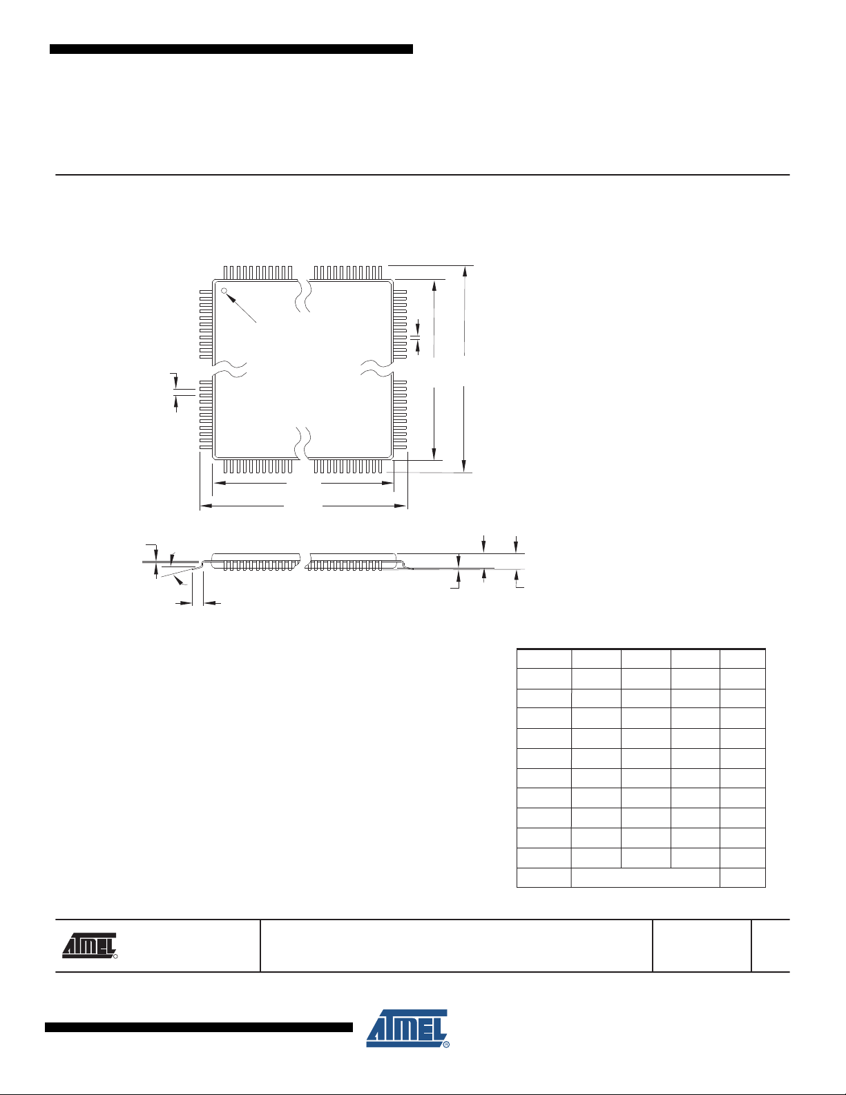
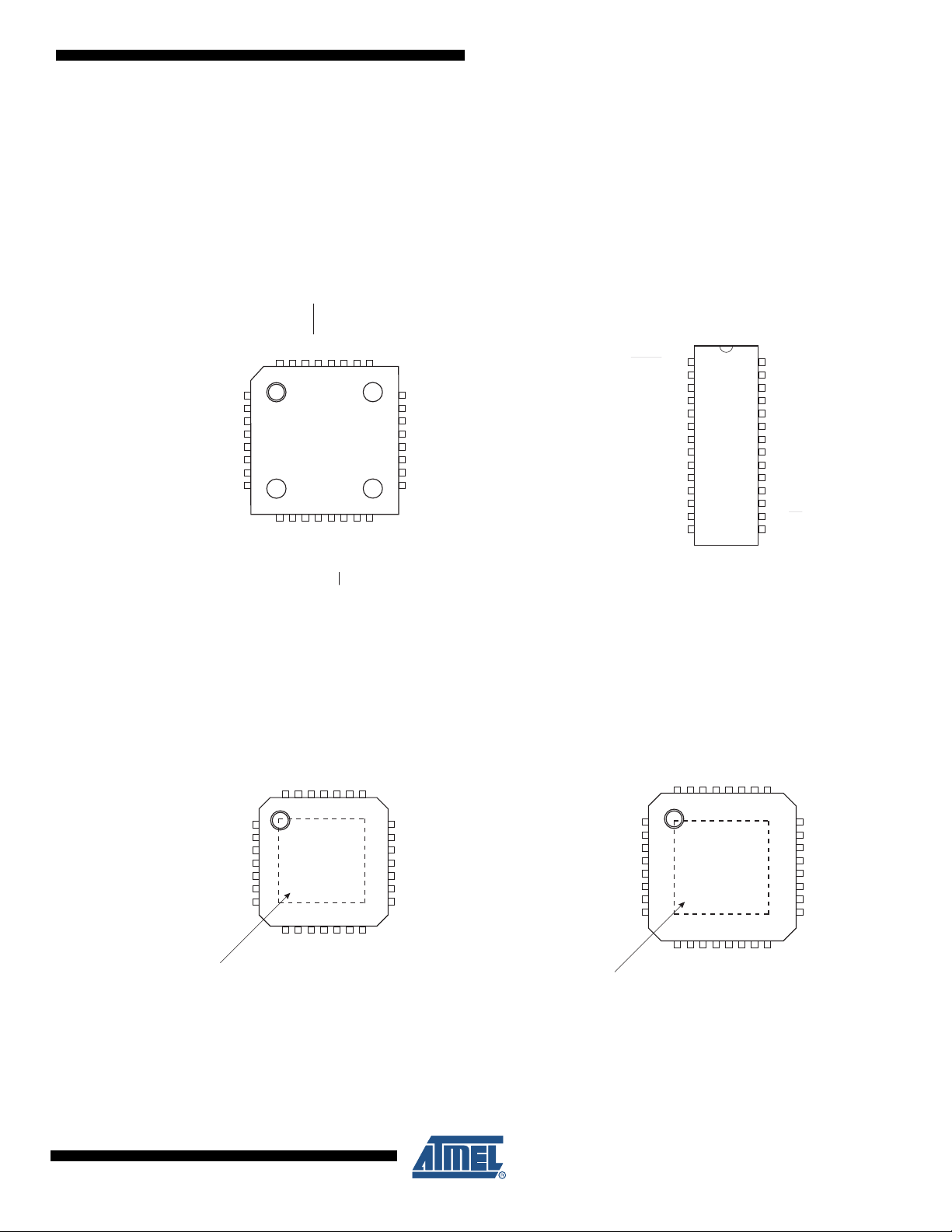
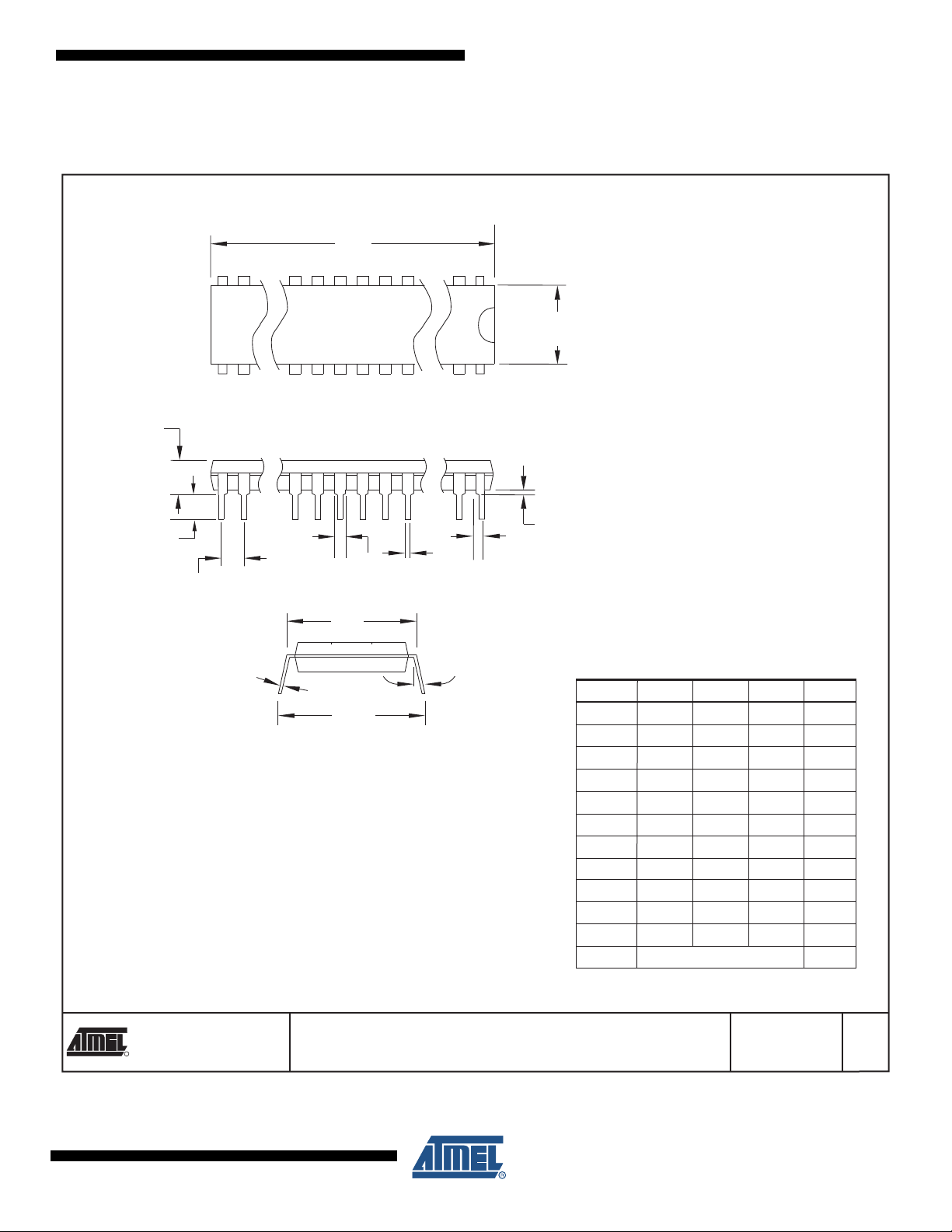
8. Packaging Information
2325 Orchard Parkway
San Jose, CA 95131
TITLE
DRAWING NO.
R
REV.
32A, 32-lead, 7 x 7 mm Body Size, 1.0 mm Body Thickness,
0.8 mm Lead Pitch, Thin Profile Plastic Quad Flat Package (TQFP)
B
32A
10/5/2001
PIN 1 IDENTIFIER
0˚~7˚
PIN 1
L
C
A1
A2 A
D1
D
e
E1 E
B
Notes: 1. This package conforms to JEDEC reference MS-026, Variation ABA.
2. Dimensions D1 and E1 do not include mold protrusion. Allowable
protrusion is 0.25 mm per side. Dimensions D1 and E1 are maximum
plastic body size dimensions including mold mismatch.
3. Lead coplanarity is 0.10 mm maximum.
A – – 1.20
A1 0.05 – 0.15
A2 0.95 1.00 1.05
D 8.75 9.00 9.25
D1 6.90 7.00 7.10 Note 2
E 8.75 9.00 9.25
E1 6.90 7.00 7.10 Note 2
B 0.30 – 0.45
C 0.09 – 0.20
L 0.45 – 0.75
e 0.80 TYP
COMMON DIMENSIONS
(Unit of Measure = mm)
SYMBOL
MIN
NOM
MAX
NOTE
8.1 32A
ATmega48PA/88PA/168PA/328P
8161DS–AVR–10/09
19
Page 20
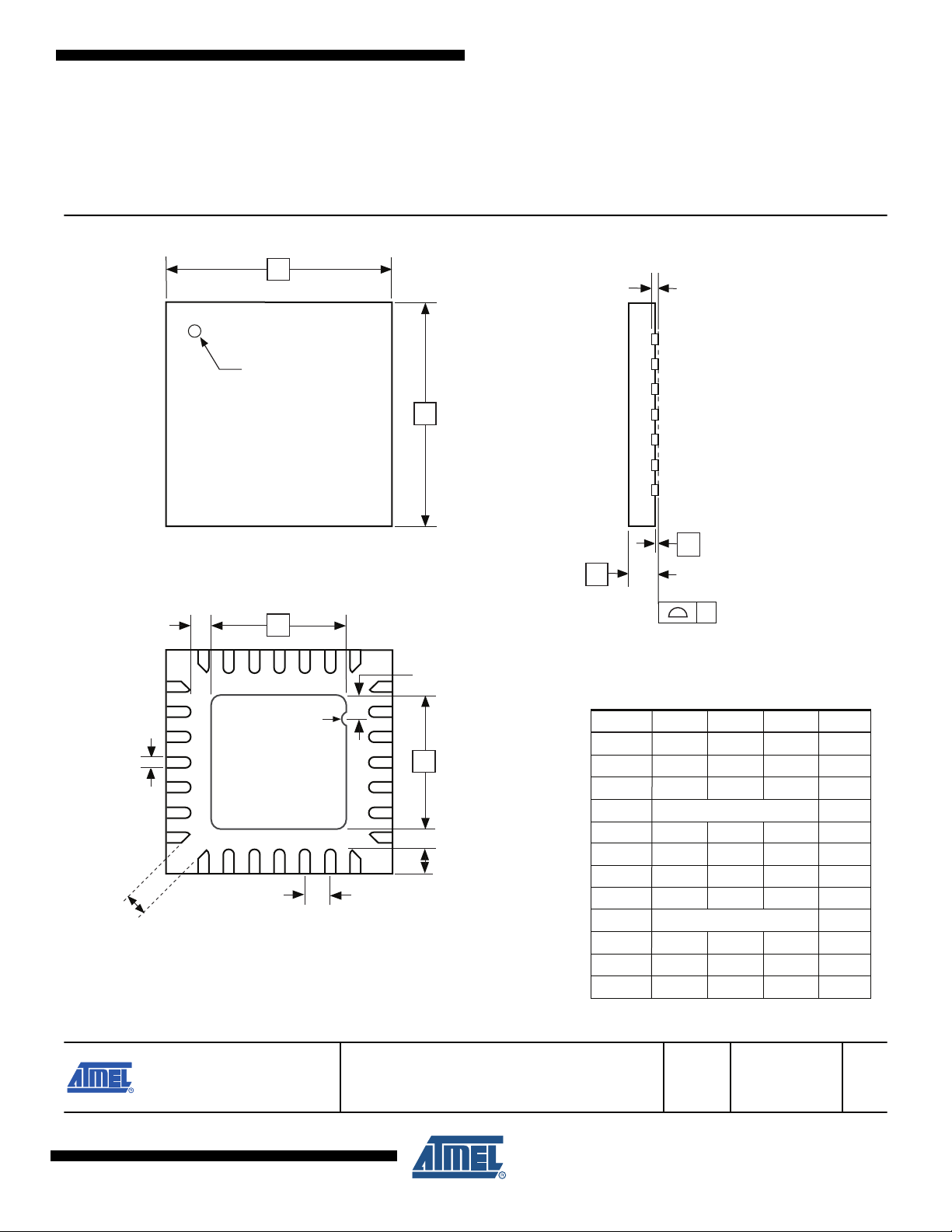
8.2 28M1
TITLE
DRAWING NO. GPC
REV.
Package Drawing Contact:
packagedrawings@atmel.com
28M1ZBV B
28M1, 28-pad, 4 x 4 x 1.0 mm Body, Lead Pitch 0.45 mm,
2.4 x 2.4 mm Exposed Pad, Thermally Enhanced
Plastic Very Thin Quad Flat No Lead Package (VQFN)
10/24/08
SIDE VIEW
Pin 1 ID
BOTTOM VIEW
TOP VIEW
Note:
The terminal #1 ID is a Laser-marked Feature.
D
E
e
K
A1
C
A
D2
E2
y
L
1
2
3
b
1
2
3
0.45
COMMON DIMENSIONS
(Unit of Measure = mm)
SYMBOL
MIN
NOM
MAX
NOTE
A 0.80 0.90 1.00
A1 0.00 0.02 0.05
b 0.17 0.22 0.27
C 0.20 REF
D 3.95 4.00 4.05
D2 2.35 2.40 2.45
E 3.95 4.00 4.05
E2 2.35 2.40 2.45
e 0.45
L 0.35 0.40 0.45
y 0.00 – 0.08
K 0.20 – –
R 0.20
0.4 Ref
(4x)
ATmega48PA/88PA/168PA/328P
8161DS–AVR–10/09
20
Page 21
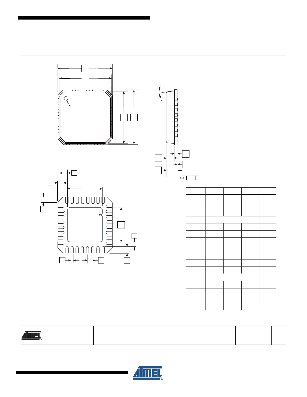
8.3 32M1-A
2325 Orchard Parkway
San Jose, CA 95131
TITLE
DRAWING NO.
R
REV.
32M1-A, 32-pad, 5 x 5 x 1.0 mm Body, Lead Pitch 0.50 mm,
E
32M1-A
5/25/06
3.10 mm Exposed Pad, Micro Lead Frame Package (MLF)
COMMON DIMENSIONS
(Unit of Measure = mm)
SYMBOL
MIN
NOM
MAX
NOTE
D1
D
E1
E
e
b
A3
A2
A1
A
D2
E2
0.08
C
L
1
2
3
P
P
0
1
2
3
A 0.80 0.90 1.00
A1 – 0.02 0.05
A2 – 0.65 1.00
A3 0.20 REF
b 0.18 0.23 0.30
D
D1
D2 2.95 3.10 3.25
4.90 5.00 5.10
4.70 4.75 4.80
4.70 4.75 4.80
4.90 5.00 5.10
E
E1
E2 2.95 3.10 3.25
e 0.50 BSC
L 0.30 0.40 0.50
P – – 0.60
– – 12o
Note: JEDEC Standard MO-220, Fig. 2 (Anvil Singulation), VHHD-2.
TOP VIEW
SIDE VIEW
BOTTOM VIEW
0
Pin 1 ID
Pin #1 Notch
(0.20 R)
K 0.20 – –
K
K
ATmega48PA/88PA/168PA/328P
8161DS–AVR–10/09
21
Page 22
8.4 28P3
2325 Orchard Parkway
San Jose, CA 95131
TITLE
DRAWING NO.
R
REV.
28P3, 28-lead (0.300"/7.62 mm Wide) Plastic Dual
Inline Package (PDIP)
B
28P3
09/28/01
PIN
1
E1
A1
B
REF
E
B1
C
L
SEATING PLANE
A
0º ~ 15º
D
e
eB
B2
(4 PLACES)
COMMON DIMENSIONS
(Unit of Measure = mm)
SYMBOL
MIN
NOM
MAX
NOTE
A – – 4.5724
A1 0.508 – –
D 34.544 – 34.798 Note 1
E 7.620 – 8.255
E1 7.112 – 7.493 Note 1
B 0.381 – 0.533
B1 1.143 – 1.397
B2 0.762 – 1.143
L 3.175 – 3.429
C 0.203 – 0.356
eB – – 10.160
e 2.540 TYP
Note: 1. Dimensions D and E1 do not include mold Flash or Protrusion.
Mold Flash or Protrusion shall not exceed 0.25 mm (0.010").
ATmega48PA/88PA/168PA/328P
8161DS–AVR–10/09
22
Page 23

9. Errata
9.1 Errata ATmega48PA
The revision letter in this section refers to the revision of the ATmega48PA device.
9.1.1 Rev. D
No known errata.
9.2 Errata ATmega88PA
The revision letter in this section refers to the revision of the ATmega88PA device.
9.2.1 Rev. F
No known errata.
9.3 Errata ATmega168PA
The revision letter in this section refers to the revision of the ATmega168PA device.
9.3.1 Rev E
No known errata.
ATmega48PA/88PA/168PA/328P
9.4 Errata ATmega328P
The revision letter in this section refers to the revision of the ATmega328P device.
9.4.1 Rev D
No known errata.
9.4.2 Rev C
Not sampled.
9.4.3 Rev B
•
Unstable 32 kHz Oscillator
1. Unstable 32 kHz Oscillator
The 32 kHz oscillator does not work as system clock.
The 32 kHz oscillator used as asynchronous timer is inaccurate.
Problem Fix/ Workaround
None
9.4.4 Rev A
•
Unstable 32 kHz Oscillator
1. Unstable 32 kHz Oscillator
The 32 kHz oscillator does not work as system clock.
8161DS–AVR–10/09
The 32 kHz oscillator used as asynchronous timer is inaccurate.
Problem Fix/ Workaround
None
23
Page 24

10. Datasheet Revision History
Please note that the referring page numbers in this section are referred to this document. The
referring revision in this section are referring to the document revision.
10.1 Rev. 8161D – 10/09
1. Inserted Table 8-8 on page 32, Capacitance for Low-frequency Crystal Oscillator.
10.2 Rev. 8161C – 05/09
1. Updated ”Features” on page 1 for ATmega48PA/88PA/168PA/328P.
2. Updated ”Overview” on page 5 included the Table 2-1 on page 6.
3. Updated ”AVR Memories” on page 16 included ”Register Description” on page 21 and inserted
Figure 7-1 on page 17.
4. Updated ”Register Description” on page 44.
5. Updated ”System Control and Reset” on page 46.
ATmega48PA/88PA/168PA/328P
6. Updated ”Interrupts” on page 57.
7. Updated ”External Interrupts” on page 70.
8. Updated ”Boot Loader Support – Read-While-Write Self-Programming, ATmega88PA,
9. Inserted
10. Inserted ”ATmega328P DC Characteristics” on page 316.
11.
12.
13.
14.
15.
16.
10.3 Rev. 8161B – 01/09
1. Updated ”Features” on page 1 for ATmega48PA and updated the book accordingly.
2. Updated ”Overview” on page 5 included the Table 2-1 on page 6.
3. Updated ”AVR Memories” on page 16 included ”Register Description” on page 21 and inserted
ATmega168PA and ATmega328P” on page 277.
”ATmega168PA DC Characteristics” on page 315.
Inserted ”ATmega168PA Typical Characteristics” on page 375.
Inserted ”ATmega328P Typical Characteristics” on page 399.
Inserted Ordering Information for ”ATmega168PA” on page 432.
Inserted Ordering Information for ”ATmega328P” on page 433.
Inserted ”Errata ATmega328P” on page 438.
Editing updates.
Figure 7-1 on page 17.
8161DS–AVR–10/09
4. Updated ”Register Description” on page 44.
5. Updated ”System Control and Reset” on page 46.
6. Updated ”Interrupts” on page 57.
24
Page 25

7. Updated ”External Interrupts” on page 70.
8. Inserted Typical characteristics for ”ATmega48PA Typical Characteristics” on page 327.
9.
10.
11.
12.
13.
10.4 Rev. 8161A – 11/08
1. Initial revision (Based on the ATmega48P/88P/168P/328P datasheet 8025F-AVR-08/08).
2. Changes done compared to ATmega48P/88P/168P/328P datasheet 8025F-AVR-08/08:
ATmega48PA/88PA/168PA/328P
Updated figure names in Typical characteristics for ”ATmega88PA Typical Character-
istics” on page 351.
Inserted ”ATmega48PA DC Characteristics” on page 314.
Updated Table 28-1 on page 317 by removing the footnote from Vcc/User calibration
Updated Table 28-7 on page 323 by removing Max value (2.5 LSB) from Absolute
accuracy, V
Inserted Ordering Information for ”ATmega48PA” on page 430.
– Updated ”DC Characteristics” on page 313 with new typical values for I
– Updated ”Speed Grades” on page 316.
– New graphics in ”Typical Characteristics” on page 326.
–New ”Ordering Information” on page 430.
= 4V, VCC = 4V, ADC clock = 200 kHz.
REF
CC
.
8161DS–AVR–10/09
25
Page 26

Headquarters International
Atmel Corporation
2325 Orchard Parkway
San Jose, CA 95131
USA
Tel: 1(408) 441-0311
Fax: 1(408) 487-2600
Atmel Asia
Unit 1-5 & 16, 19/F
BEA Tower, Millennium City 5
418 Kwun Tong Road
Kwun Tong, Kowloon
Hong Kong
Tel: (852) 2245-6100
Fax: (852) 2722-1369
Product Contact
Web Site
www.atmel.com
Literature Requests
www.atmel.com/literature
Atmel Europe
Le Krebs
8, Rue Jean-Pierre Timbaud
BP 309
78054 Saint-Quentin-enYvelines Cedex
France
Tel: (33) 1-30-60-70-00
Fax: (33) 1-30-60-71-11
Technical Support
avr@atmel.com
Atmel Japan
9F, Tonetsu Shinkawa Bldg.
1-24-8 Shinkawa
Chuo-ku, Tokyo 104-0033
Japan
Tel: (81) 3-3523-3551
Fax: (81) 3-3523-7581
Sales Contact
www.atmel.com/contacts
Disclaimer: The information in this document is provided in connection with Atmel products. No license, express or implied, by estoppel or otherwise, to any
intellectual property right is granted by this document or in connection with the sale of Atmel products. EXCEPT AS SET FORTH IN ATMEL’S TERMS AND CONDI-
TIONS OF SALE LOCATED ON ATMEL’S WEB SITE, ATMEL ASSUMES NO LIABILITY WHATSOEVER AND DISCLAIMS ANY EXPRESS, IMPLIED OR STATUTORY
WARRANTY RELATING TO ITS PRODUCTS INCLUDING, BUT NOT LIMITED TO, THE IMPLIED WARRANTY OF MERCHANTABILITY, FITNESS FOR A PARTICULAR
PURPOSE, OR NON-INFRINGEMENT. IN NO EVENT SHALL ATMEL BE LIABLE FOR ANY DIRECT, INDIRECT, CONSEQUENTIAL, PUNITIVE, SPECIAL OR INCIDENTAL DAMAGES (INCLUDING, WITHOUT LIMITATION, DAMAGES FOR LOSS OF PROFITS, BUSINESS INTERRUPTION, OR LOSS OF INFORMATION) ARISING OUT OF
THE USE OR INABILITY TO USE THIS DOCUMENT, EVEN IF ATMEL HAS BEEN ADVISED OF THE POSSIBILITY OF SUCH DAMAGES. Atmel makes no
representations or warranties with respect to the accuracy or completeness of the contents of this document and reserves the right to make changes to specifications
and product descriptions at any time without notice. Atmel does not make any commitment to update the information contained herein. Unless specifically provided
otherwise, Atmel products are not suitable for, and shall not be used in, automotive applications. Atmel’s products are not intended, authorized, or warranted for use
as components in applications intended to support or sustain life.
© 2009 Atmel Corporation. All rights reserved. Atmel®, Atmel logo and combinations thereof, AVR® and others are registered trademarks or
trademarks of Atmel Corporation or its subsidiaries. Other terms and product names may be trademarks of others.
8161DS–AVR–10/09
 Loading...