

Page 1

Features
N
This i
• High-performance, Low-power AVR
• Advanced RISC Architecture
– 131 Po we rful Instructions – Most Single-clock Cycle Execution
– 32 x 8 General Purpose Working Regi sters
– Fully Static Operation
– Up to 16 MIPS Throughput at 16 MHz
– On-chip 2-cycle Multiplier
• Non-volatile Program and Data Memories
– 16K Bytes of In-System Self-programmab le Flash
Endurance: 10,000 Write/Erase Cycles
– Optional Boot Code Section with Independent Lock Bits
In-System Programming by On-chip Boot Program
True Read-While-Write Operation
– 512 Bytes EEPROM
Endurance: 100,000 Write/Erase Cycles
– 1K Bytes Internal SRAM
– Up to 64K Bytes Optional External Memory Space
– Programming Lock for Software Security
• JTAG (IEEE std. 1149.1 Compliant) Interface
– Boundary-scan Capabilities According to the JTAG Standard
– Extensive On-chip De bug Support
– Programming of Flas h, EEPROM, Fuses, and Lock Bits through the JTAG Interface
• Peripheral Features
– T w o 8-bit Timer/Counters with Separate Prescalers and Compare Modes
– T w o 16-bit Timer/Counters with Separate Prescaler s, Compare Modes, and
Capture Modes
– Real Time Counter with Separate Oscillator
– Six PWM Channels
– Dual Programmable Serial USARTs
– Master/Slave SPI Serial Interface
– Programmable Watchdog Timer with Separate On-chip Oscillator
– On-chip Analog Comparat or
• Special Micro controller Features
– Powe r-on Reset and Programmable Brown-out Detection
– Internal Calibra ted RC Oscillator
– External and Internal Interrupt Sources
– Five Sleep Modes: Idle, Power-save, Power-down, Standby, and Extended Standby
• I/O and Packages
– 35 Programmable I/O Lines
– 40-pin PDIP, 44-lead TQFP, and 44-pad MLF
• Operating Voltages
– 1.8 - 5.5V for ATmega162V
– 2.7 - 5.5V for ATmega162
• Speed Grades
– 0 - 8 MHz for ATmega162V (see Figure 113)
– 0 - 16 MHz for ATmega162 (see Figure 114)
®
8-bit Microcontroller
8-bit
Microcontroller
with 16K Bytes
In-System
Programmable
Flash
ATmega162
ATmega162V
Advance
Information
Summary
2513DS–AVR–04/03
Rev. 2513DS–AVR–04/03
ote:
avai lable on our web site at
s a summary document. A complete document is
www.atmel.com
.
1
Page 2

Pin Configurations Figure 1. Pinout ATmega162
(OC0/T0) PB0
(OC2/T1) PB1
(RXD1/AIN0) PB2
(TXD1/AIN1) PB3
(SS/OC3B) PB4
(MOSI) PB5
(MISO) PB6
(RXD0) PD0
(TXD0) PD1
(INT0/XCK1) PD2
(TOSC1/XCK0/OC3A) PD4
(INT0/XCK1) PD2
(TOSC1/XCK0/OC3A) PD4
(INT1/ICP3) PD3
(OC1A/TOSC2) PD5
(INT1/ICP3) PD3
(OC1A/TOSC2) PD5
(MOSI) PB5
(MISO) PB6
(SCK) PB7
RESET
(RXD0) PD0
VCC
(TXD0) PD1
1
2
3
4
5
6
(SCK) PB7
RESET
(WR) PD6
(RD) PD7
XTAL2
XTAL1
1
2
3
4
5
6
7
8
9
10
11
7
8
9
10
11
12
13
14
15
16
17
18
19
GND
20
PB4 (SS/OC3B)
PB3 (TXD1/AIN1)
PB2 (RXD1/AIN0)
44 42 40 38 36 34
43 41 39 37 35
13 15 17 19 21
12 14 16 18 20 22
PDIP
40
39
38
37
36
35
34
33
32
31
30
29
28
27
26
25
24
23
22
21
TQFP/MLF
PB1 (OC2/T1)
PB0 (OC0/T0)
GND
VCC
PA0 (AD0/PCINT0)
VCC
PA0 (AD0/PCINT0)
PA1 (AD1/PCINT1)
PA2 (AD2/PCINT2)
PA3 (AD3/PCINT3)
PA4 (AD4/PCINT4)
PA5 (AD5/PCINT5)
PA6 (AD6/PCINT6)
PA7 (AD7/PCINT7)
PE0 (ICP1/INT2)
PE1 (ALE)
PE2 (OC1B)
PC7 (A15/TDI/PCINT15)
PC6 (A14/TDO/PCINT14)
PC5 (A13/TMS/PCINT13)
PC4 (A12/TCK/PCINT12)
PC3 (A11/PCINT11)
PC2 (A10/PCINT10)
PC1 (A9/PCINT9)
PC0 (A8/PCINT8)
PA1 (AD1/PCINT1)
PA2 (AD2/PCINT2)
PA3 (AD3/PCINT3)
PA4 (AD4/PCINT4)
33
PA5 (AD5/PCINT5)
32
PA6 (AD6/PCINT6)
31
PA7 (AD7/PCINT7)
30
PE0 (ICP1/INT2)
29
GND
28
PE1 (ALE)
27
PE2 (OC1B)
26
PC7 (A15/TDI/PCINT15)
25
PC6 (A14/TDO/PCINT14)
24
PC5 (A13/TMS/PCINT13)
23
VCC
GND
XTAL2
XTAL1
(RD) PD7
(WR) PD6
(A8/PCINT8) PC0
(A9/PCINT9) PC1
(A11/PCINT11) PC3
(A10/PCINT10) PC2
(TCK/A12/PCINT12) PC4
Disclaimer Typical values contained in thi s data sheet are based on s imulation s and cha racteriza-
tion of other AVR microcontrollers manufactured on the same process technology. Min
and Max va lu es w ill be av a ilable after the device is ch a r ac ter iz ed.
2
ATmega162/V
2513DS–AVR–04/03
Page 3

ATmega162/V
Overview The ATmega162 is a low-power CMOS 8-bit microcontroller based on the AVR
enhanced RISC architecture. By executing powerful instructions in a single clock cycle,
the ATmega162 achieves throughputs approaching 1 MIPS per MHz allowing the system designer to optimize power consumption versus processing speed.
Block Diagram Figure 2. Block Diagram
VCC
PA0 - PA7 PC0 - PC7
PORTA DRIVERS/BUFFERS
PE0 - PE2
PORTE
DRIVERS/
BUFFERS
PORTC DRIVERS/BUFFERS
GND
PORTA DIGITAL INTERFACE
PROGRAM
COUNTER
PROGRAM
FLASH
INSTRUCTION
REGISTER
INSTRUCTION
DECODER
CONTROL
LINES
AVR CPU
PROGRAMMING
LOGIC
STACK
POINTER
SRAM
GENERAL
PURPOSE
REGISTERS
X
Y
Z
ALU
STATUS
REGISTER
SPI
PORTE
DIGITAL
INTERFACE
PORTC DIGITAL INTERFACE
INTERNAL
OSCILLATOR
WATCHDOG
TIMER
MCU CTRL.
& TIMING
INTERRUPT
UNIT
TIMERS/
COUNTERS
EEPROM
USART0
OSCILLATOR
INTERNAL
CALIBRATED
OSCILLATOR
OSCILLATOR
XTAL1
XTAL2
RESET
2513DS–AVR–04/03
+
-
PORTB DIGITAL INTERFACE
PORTB DRIVERS/BUFFERS
COMP.
INTERFACE
USART1
PORTD DIGITAL INTERFACE
PORTD DRIVERS/BUFFERS
PD0 - PD7PB0 - PB7
3
Page 4

The AVR core combines a rich instruction set with 32 general purpose working registers.
All the 32 re gist ers ar e d irect ly co nnec ted t o t he Ari thme tic Logi c Un it (A LU), allow ing
two independent registers to be accessed in one single instruction executed in one clock
cycle. The resulting architecture is more code efficient while achieving throughputs up to
ten times faster than conventional CISC microcontrollers.
The ATmega162 provides the following features: 16K bytes of In-System Programmable
Flash with Read-While-Write capabilities, 512 bytes EEPROM, 1K bytes SRAM, an
external memory interface, 35 general purpose I/O lines, 32 general purpose working
registers, a JTAG interface for Boundary-scan, On-chip Debugging support and programming, four flex ible Timer/Counters with com pare modes, internal and external
interrupts, two serial programmable USARTs, a programmable Watchdog Timer with
Internal Oscillator, an SPI serial port, and five software selectable power saving m odes.
The Idle mode stops the CPU whi le allowing the SRAM, Timer/Counters, SPI port, a nd
interrupt system to continue functioning. The Power-down mode saves the register contents but freezes t he Oscillat or, disabling all other chip funct ions until the n ext interrupt
or Hardware Reset. In Power-save m ode, the Asynchronous Timer continues to run,
allowing the user to maintain a timer base while the rest of the device is sleeping. In
Standby mode, the cr ystal/resonat or Oscillator is runnin g while the rest of the device is
sleeping. This allows very fast start-up combined with low-power consumption. In
Extended Standby mode, both the main Oscillator and the Asynchronous Timer continue to run.
The device is manufactured using Atmel’s high density non-volatile memory technology.
The On-chip ISP Flash allows the program memory to be reprogrammed In-System
through an SPI serial interface, by a convent ional non-volatil e memory progra mmer, or
by an On-chip Boot Program running on the AVR core. The Boot Program can use any
interface to download the Application Program in the Application Flash memory. Software in the Boot Flash s ection wil l continue to run while th e A pplication Flash sec tion is
updated, pro viding true Re ad-Whi le-Write operation . By co mbinin g an 8-bi t RISC CP U
with In-System Self-Programmable Flash on a monolithic chip, the Atmel ATmega162 is
a powerful microcontroller that provides a highly flexible and cost effective solution to
many embedded control applications .
ATmega161 and ATmega162 Compatibility
4
ATmega162/V
The ATmega162 AVR is supported with a full suite of program and system development
tools i nclud ing: C comp ile rs, m acro a sse mbl ers, progra m de bugg er /simu lators , In -Circuit Emulators, and evaluation kits.
The ATmega162 is a hig hly complex m icrocontroller where t he number of I/O loca tions
supersedes the 64 I/O locations reserved in the AVR instruction set. To ensur e backward compatibility with the ATmega161, all I/O locations present in ATmega161 have
the sam e locat ions in A Tmega 162. So me addi tiona l I/O loca tions a re add ed in an
Extended I/O space starting from 0x60 to 0xFF, (i.e., in the ATmega1 62 internal RAM
space). Thes e locations can be reached by using LD/LDS/LDD and ST/STS/ STD
instructions only, not by using IN and OUT instructions. The relocation of the internal
RAM space may still be a problem for ATmega161 users. Also, the increased number of
Interrupt Vectors might be a problem if the code uses absolute addresses. To solve
these problems, an ATmega161 compatibility mode can be selected by programming
the fuse M161C. In this m ode, none o f the functions i n the Exte nded I/O sp ace are i n
use, so the internal RAM is located as in ATmega161. Also, the Extended Interrupt Vectors are re moved . The ATm ega16 2 is 1 00% pin compa tible wi th ATme ga1 61, an d can
replace the ATmega161 on current Printed Circuit Boards. However, t he location of
Fuse bits and the electrical characteristics differs between the two devices.
2513DS–AVR–04/03
Page 5

ATmega162/V
ATmega161 Compatibility Mode
Programming the M161C will change the following functionality:
• The extended I/O map will be configured as internal RAM once the M161C Fuse is
programmed.
• The timed sequence for changing the Watchdog Time-out period is disabled. See
“Timed Sequences for Changing the Configuration of the Watchdog Timer” on page
54 for details.
• The double buffering of the USART Receive Registers is disabled. See “AVR
USART vs. AVR UART – Compatibility” on page 166 for details.
• Pin change interrupts are not supported (Contol Registers are located in Extended
I/O).
• One 16 bits Timer/Counter (Timer/Counter1) only. Timer/Counter3 is not accessible .
Note that the shared UBRRHI Register in ATmega161 is split into two separate registers
in ATmega 162, UBRR 0H and UB RR1H. The l ocation of th ese regist ers will not be
affected by the ATmega161 compatibility fuse.
Pin Descript i on s
VCC Digital supply voltage GND Ground Port A (PA7..PA0) Port A is an 8-bit bi-directional I/O port with internal pull -up resistors (sele cted for each
bit). The Port A output buffers have symmetrical drive characteristics with both high sink
and source capability. When pins PA0 to PA7 are used as inputs and are externally
pulled low, they will source current if the internal pull-up resistors are activated. The Port
A pins are tri-stated when a reset condition becomes active, even if the clock is not
running.
Port A also serves the f unctions of v ario us spec ial f eat ures of the ATmega162 as listed
on page 70.
Port B (PB7..P B0) Port B is an 8-bit bi-directional I/O port with internal pull -up resistors (sele cted for each
bit). The Port B output buffers have symmetrical drive characteristics with both high sink
and source capability. A s inputs, Port B pins that are externally pulled low will source
current if the pull-up resistors are activated. The Port B pins are tri-stated when a res et
condition becomes active, even if the clock is not running.
Port B also serves the f unctions of v ario us spec ial f eat ures of the ATmega162 as listed
on page 70.
Port C (PC7..P C0) Port C is an 8-bit bi-directional I/O port with internal pull-up resistors (selected fo r each
bit). The Port C output buffers have symmetrical drive characteristics with both high sink
and source capability . As inputs, Port C pins that are externally pulled low will source
current if the pull-up resistors are activated. The Port C pins are tri-stated when a reset
condition becomes ac tive, even i f the clock is no t running . If the JTAG int erface is
enabled, the pul l-up resist ors on pins PC 7(TDI), PC 5(TMS) an d PC4(T CK) will be activated even if a Reset occurs.
Port C also serves the functions of the JTAG interface and other special features of the
ATmega162 as listed on page 73.
2513DS–AVR–04/03
5
Page 6

Port D (PD7..P D0) Port D is an 8-bit bi-directional I/O port with internal pull-up resistors (selected fo r each
bit). The Port D output buffers have symmetrical drive characteristics with both high sink
and source capability . As inputs, Port D pins that are externally pulled low will source
current if the pull-up resistors are activated. The Port D pins are tri-stated when a reset
condition becomes active, even if the clock is not running.
Port D also serves the f unc tions of various special features of t he A Tmega162 as listed
on page 76.
Port E(PE2..PE0) Port E is an 3-bit bi-directional I/O port with internal pull -up resistors (sele cted for each
bit). The Port E output buffers have symmetrical drive characteristics with both high sink
and source capability. A s inputs, Port E pins that are externally pulled low will source
current if the pull-up resistors are activated. The Port E pins are tri-stated when a res et
condition becomes active, even if the clock is not running.
Port E also serves the f unctions of v ario us spec ial f eat ures of the ATmega162 as listed
on page 79.
RESET
XTAL1 Input to the Inverting Oscillator am plif ier and input to th e internal clock operating circuit. XTAL2 Output from the Inve rting Oscillat o r a mplifier.
Reset input. A low le ve l on this pin for l onger than the minimum pul se length will generate a Reset, even if the clock is not running. The minimum pulse length is given in Table
18 on page 46. Shorter pulses are not guaranteed to generate a reset.
About Code Examples This documentation contains simple code examples that briefly show how to use various
parts of the device. These code examples assume that the part specific header file is
included before com pilation. Be aware t hat not all C com pile r vendors incl ude bi t definitions in the header files and inte rrupt hand ling in C is c ompiler de pendent . Please
confirm with the C compiler documentation for more details.
6
ATmega162/V
2513DS–AVR–04/03
Page 7
ATmega162/V
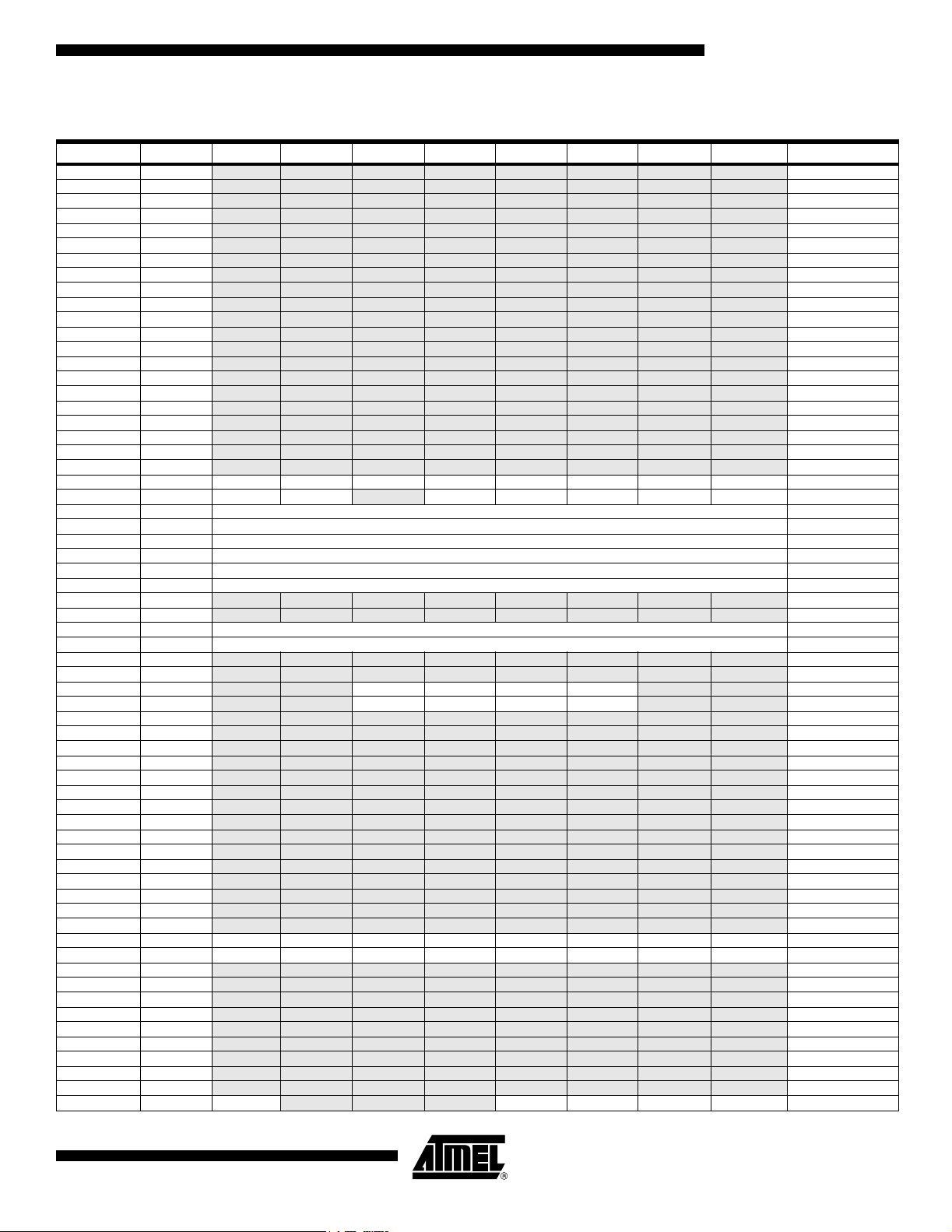
Register Summary
Address Name Bit 7 Bit 6 Bit 5 Bit 4 Bit 3 Bit 2 Bit 1 Bit 0 Page
(0xFF) Reserved – – – – – – – –
.. Reserved – – – – – – – –
(0x9E) Reserved – – – – – – – –
(0x9D) Reserved – – – – – – – –
(0x9C) Reserved – – – – – – – –
(0x9B) Reserved – – – – – – – –
(0x9A) Reserved
(0x99) Reserved
(0x98) Reserved – – – – – – – –
(0x97) Reserved – – – – – – – –
(0x96) Reserved – – – – – – – –
(0x95) Reserved – – – – – – – –
(0x94) Reserved – – – – – – – –
(0x93) Reserved – – – – – – – –
(0x92) Reserved – – – – – – – –
(0x91) Reserved – – – – – – – –
(0x90) Reserved – – – – – – – –
(0x8F) Reserved – – – – – – – –
(0x8E) Reserved – – – – – – – –
(0x8D) Reserved – – – – – – – –
(0x8C) Reserved – – – – – – – –
(0x8B) TCCR3A COM3A1 COM3A0 COM3B1 COM3B0 FOC3A FOC3B WGM31 WGM30 129
(0x8A) TCCR3B ICNC3 ICES3 – WGM33 WGM32 CS32 CS31 CS30 126
(0x89) TCNT3H Timer/Counter3 – Counter Register High Byte 131
(0x88) TCNT3L Timer/Counter3 – Counter Register Low Byte 131
(0x87) OCR3AH Timer/Counter3 – Output Compare Register A High Byte 131
(0x86) OCR 3AL Timer/Counter3 – Output Compare Register A Low Byte 131
(0x85) OCR3BH Timer/Counter3 – Output Compare Register B High Byte 131
(0x84) OCR 3BL Timer/Counter3 – Output Compare Register B Low Byte 131
(0x83) Reserved – – – – – – – –
(0x82) Reserved – – – – – – – –
(0x81) ICR3H Timer/Counter3 – Input Capture Register High Byte 132
(0x80) ICR3L Timer/Counter3 – Input Capture Register Low Byte 132
(0x7F) Reserved – – – – – – – –
(0x7E) Reserved – – – – – – – –
(0x7D) ETIMSK – – TICIE3 OCIE3A OCIE3B TOIE3 – – 133
(0x7C) ETIFR – –ICF3OCF3AOCF3BTOV3– – 134
(0x7B) Reserved – – – – – – – –
(0x7A) Reserved – – – – – – – –
(0x79) Reserved – – – – – – – –
(0x78) Reserved – – – – – – – –
(0x77) Reserved – – – – – – – –
(0x76) Reserved – – – – – – – –
(0x75) Reserved – – – – – – – –
(0x74) Reserved – – – – – – – –
(0x73) Reserved – – – – – – – –
(0x72) Reserved – – – – – – – –
(0x71) Reserved – – – – – – – –
(0x70) Reserved – – – – – – – –
(0x6F) Reserved – – – – – – – –
(0x6E) Reserved – – – – – – – –
(0x6D) Reserved – – – – – – – –
(0x6C) PCMSK1 PCINT15 PCINT14 PCINT13 PCINT12 PCINT11 PCINT10 PCINT9 PCINT8 86
(0x6B) PCMSK0 PCINT7 PCINT6 PCINT5 PCINT4 PCINT3 PCINT2 PCINT1 PCINT0 86
(0x6A) Reserved – – – – – – – –
(0x69) Reserved – – – – – – – –
(0x68) Reserved – – – – – – – –
(0x67) Reserved – – – – – – – –
(0x66) Reserved – – – – – – – –
(0x65) Reserved – – – – – – – –
(0x64) Reserved – – – – – – – –
(0x63) Reserved – – – – – – – –
(0x62) Reserved – – – – – – – –
(0x61) CLKPR CLKPCE – – – CLKPS3 CLKPS2 CLKPS1 CLKPS0 39
– – – – – – – –
– – – – – – – –
2513DS–AVR–04/03
7
Page 8
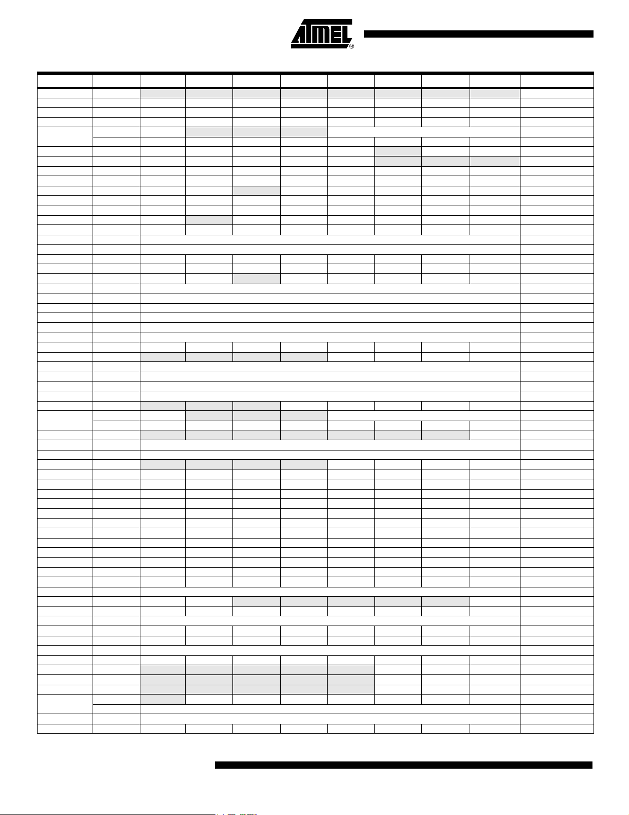
Address Name Bit 7 Bit 6 Bit 5 Bit 4 Bit 3 Bit 2 Bit 1 Bit 0 Page
(0x60) Reserved – – – – – – – –
0x3F (0x5F) SREG I T H S V N Z C 8
0x3E (0x5E) SPH SP15 SP14 SP13 SP12 SP11 SP10 SP9 SP8 11
0x3D (0x5D) SPL SP7 SP6 SP5 SP4 SP3 SP2 SP1 SP0 11
(2)
0x3C
(0x5C)
0x3B (0x5B) GICR INT1 INT0 INT2 PCIE1 PCIE0 – IVSEL IVCE 59, 84
0x3A (0x5A) GIFR INTF1 INTF0 INTF2 PCIF1 PCIF0 – – –85
0x39 (0x59) TIMSK TOIE1 OCIE1A OCIE1B OCIE2 TICIE1 TOIE2 TOIE0 OCIE0 100, 132, 153
0x38 (0x58) TIFR TOV1 OCF1A OCF1B OCF2 ICF1 TOV2 TOV0 OCF0 101, 134, 154
0x37 (0x57) SPMCR SPMIE RWWSB
0x36 (0x56) EMCUCR SM0 SRL2 SRL1 SRL0 SRW01 SRW00 SRW11 ISC2 28,42,83
0x35 (0x55) MCUCR SRE SRW10 SE SM1 ISC11 ISC10 ISC01 ISC00 28,41,82
0x34 (0x54) MCUCSR JTD
0x33 (0x53) TCCR0 FOC0 WGM00 COM01 COM00 WGM01 CS02 CS01 CS00 98
0x32 (0x52) TCNT0 Timer/Counter0 (8 Bits) 100
0x31 (0x51)
0x30 (0x50) SFIOR TSM XMBK XMM2 XMM1 XMM0 PUD PSR2 PSR310 30,68,103,155
0x2F (0x4F) TCCR1A COM1A1 COM1A0 COM1B1 CO M1B0 FOC1A FOC1B WGM11 WGM10 126
0x2E (0x4E) TCCR1B ICNC1 ICES1 – WGM13 WGM12 CS12 CS11 CS10 129
0x2D (0x4D) TCNT1H Timer/Counter1 – Counter Register High Byte 131
0x2C (0x4C) TCNT1L Timer/Counter1 – Counter Register Low Byte 131
0x2B (0x4B) OCR1AH Timer/Counter1 – Output Compare Register A High Byte 131
0x2A (0x4A) OCR1AL Timer/Counter1 – Output Compare Register A Low Byte 131
0x29 (0x49) OCR1BH Timer/Counter1 – Output Compare Register B High Byte 131
0x28 (0x48) OCR1BL Timer/Counter1 – Output Compare Register B Low Byte 131
0x27 (0x47) TCCR2 FOC2 WGM20 COM21 COM20 WGM21 CS22 CS21 CS20 147
0x26 (0x46) ASSR – – – – AS2 TCON2UB OCR2UB TCR2UB 151
0x25 (0x45) ICR1H Timer/Counter1 – Input Capture Register High Byte 132
0x24 (0x44) ICR1L Timer/Counter1 – Input Capture Register Low Byte 132
0x23 (0x43) TCNT2 Timer/Counter2 (8 Bits) 150
0x22 (0x42) OCR2 Timer/Counter2 Output Compare Register 150
0x21 (0x41) WDTCR – – – WDCE WDE WDP2 WDP1 WDP0 51
(2)
0x20
(0x40)
0x1F (0x3F) EEARH – – – – – – – EEAR8 18
0x1E (0x3E) EEARL EEPROM Address Register Low Byte 18
0x1D (0x3D) EEDR EEPROM Data Register 19
0x1C (0x3C) EECR – – – – EERIE EEMWE EEWE EERE 19
0x1B (0x3B) PORTA PORTA7 PORTA6 PORTA5 PORTA4 PORTA3 PORTA2 PORTA1 PORTA0 80
0x1A (0x3A) DDRA DDA7 DDA6 DDA5 DDA4 DDA3 DDA2 DDA1 DDA0 80
0x19 (0x39) PINA PINA7 PINA6 PINA5 PINA4 PINA3 PINA2 PINA1 PINA0 80
0x18 (0x38) PORTB PORTB7 PORTB6 PORTB5 PORTB4 PORTB3 PORTB2 PORTB1 PORTB0 80
0x17 (0x37) DDRB DDB7 DDB6 DDB5 DDB4 DDB3 DDB2 DDB1 DDB0 80
0x16 (0x36) PINB PINB7 PINB6 PINB5 PINB4 PINB3 PINB2 PINB1 PINB0 80
0x15 (0x35) PORTC PORTC7 PORTC6 PORTC5 PORTC4 PORTC3 PORTC2 P ORTC1 PORTC0 80
0x14 (0x34) DDRC DDC7 DDC6 DDC5 DDC4 DDC3 DDC2 DDC1 DDC0 80
0x13 (0x33) PINC PINC7 PINC6 PINC5 PINC4 PINC3 PINC2 PINC1 PINC0 81
0x12 (0x32) PORTD PORTD7 PORTD6 PORTD5 PORTD4 PORTD3 PORTD2 P ORTD1 PORTD0 81
0x11 (0x31) DDRD DDD7 DDD6 DDD5 DDD4 DDD3 DDD2 DDD1 DDD0 81
0x10 (0x30) PIND PIND7 PIND6 PIND5 PIND4 PIND3 PIND2 PIND1 PIND0 81
0x0F (0x2F) SPDR SPI Data Register 162
0x0E (0x2E) SPSR SPIF WCOL – – – – – SPI2X 162
0x0D (0x2D) SPCR SPIE SPE DORD MSTR CPOL CPHA SPR1 SPR0 160
0x0C (0x2C) UDR0 USART0 I/O Data Register 184
0x0B (0x2B) UCSR0A RXC0 TXC0 UDRE0 FE0 DOR0 UPE0 U2X0 MPCM0 184
0x0A (0x2A) UCSR0B RXCIE 0 TXCIE0 UDRIE0 RXEN0 TXEN0 UCSZ02 RXB80 TXB80 185
0x09 (0x29) UBRR0L USART0 Baud Rate Register Low Byte 188
0x08 (0x28) ACSR ACD ACBG ACO ACI ACIE ACIC ACIS1 ACIS0 193
0x07 (0x27) PORTE – – – – – PORTE2 PORTE1 PORTE0 81
0x06 (0x26) DDRE – – – – – DDE2 DDE1 DDE0 81
0x05 (0x25) PINE – – – – – PINE2 PINE1 PINE0 81
(1)
0x04
(0x24)
0x03 (0x23) UDR1 USART1 I/O Data Register 184
0x02 (0x22) UCSR1A RXC1 TXC1 UDRE1 FE1 DOR1 UPE1 U2X1 MPCM1 184
UBRR1H URSEL1
(2)
UCSR1C URSEL1 UMSEL1 UPM11 UPM10 USBS1 UCSZ11 UCSZ10 UCPOL1 187
– RWWSRE BLBSET PGWRT PGERS SPMEN 219
– SM2 JTRF WDRF BORF EXTRF PORF 41,49,205
OCR0 Timer/Counter0 Output Compare Register 100
UBRR0H URSEL0 – – – UBRR0[11:8] 188
(2)
UCSR0C URSEL0 UMSEL0 UPM01 UPM00 USBS0 UCSZ01 UCSZ00 UCPOL0 187
OSCCAL – CAL6 CAL5 CAL4 CAL3 CAL2 CAL1 CAL0 37
(1)
OCDR On-chip Debug Register 200
UBRR1[11:8]
188
8
ATmega162/V
2513DS–AVR–04/03
Page 9
ATmega162/V
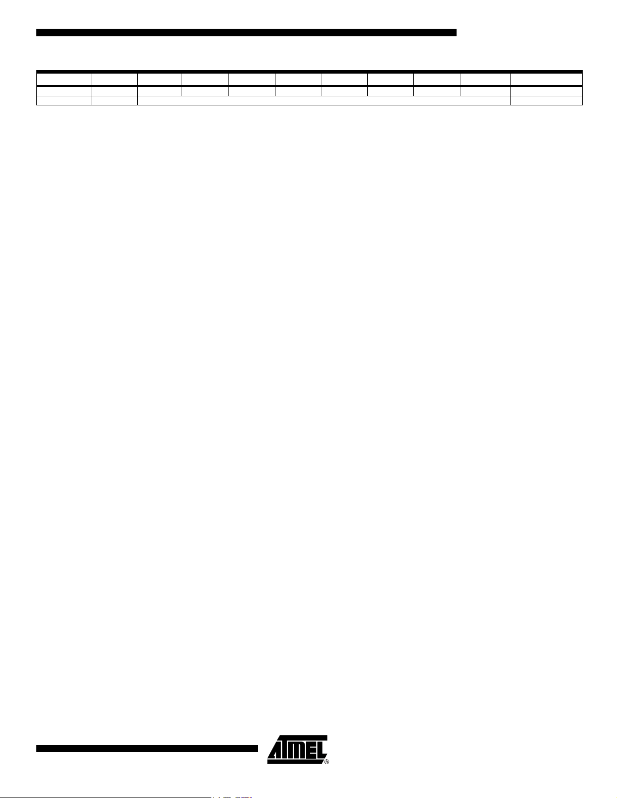
Address Name Bit 7 Bit 6 Bit 5 Bit 4 Bit 3 Bit 2 Bit 1 Bit 0 Page
0x01 (0x21) UCSR1B RXCIE1 TXCIE1 UDRIE1 RXEN1 TXEN1 UCSZ12 RXB81 TXB81 185
0x00 (0x20) UBRR1L USART1 Baud Rate Register Low Byte 188
Notes: 1. When the OCDEN Fuse is unprogrammed, the OSCCAL Register is always accessed on this address. Refer to the debug-
ger specific documentation for details on how to use the OCDR Register.
2. Refer to the USART descript ion for details on ho w to access UBRRH and UCSRC.
3. For compatibility with future devices, reserved bits should be written to zero if accessed. Reser ved I/O memory addresses
should never be written.
4. Some of the Status Flags are cleared by writing a logical one to them. Note that the CBI and SBI in structions will oper ate on
all bits in the I/O Register, writing a one back into any flag read as set, thus clearing the flag. The CBI and SBI instructions
work with registers 0x00 to 0x1F only.
2513DS–AVR–04/03
9
Page 10
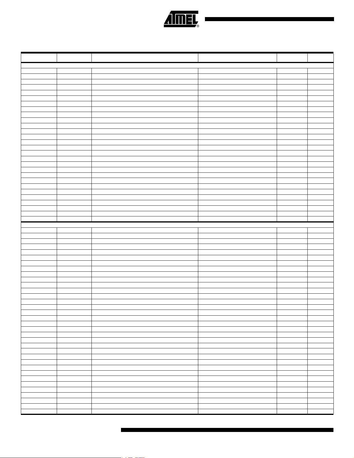
Instruction Set Summary
Mnemonics
ARITHMETIC AND LOGIC INSTRUCTIONS
ADD Rd, Rr Add two Registers Rd ← Rd + Rr Z,C,N,V,H 1
ADC Rd, Rr Add with Carry two Registers Rd ← Rd + Rr + C Z,C,N,V,H 1
ADIW Rdl,K Add Immediate to Word Rdh:Rdl ← Rdh:Rdl + K Z,C,N,V,S 2
SUB Rd, Rr Subtract two Registers Rd ← Rd - Rr Z,C,N,V,H 1
SUBI Rd, K Subtract Constant from Register Rd ← Rd - K Z,C,N,V,H 1
SBC Rd, Rr Su btract with Carry two Registers Rd ← Rd - Rr - C Z,C,N,V,H 1
SBCI Rd, K Subtract with Carry Constant from Reg. Rd ← Rd - K - C Z,C,N,V,H 1
SBIW Rdl,K Subtract Immediate from Word Rdh:Rdl ← Rdh:Rdl - K Z,C,N,V,S 2
AND Rd, Rr Logical AND Registers Rd ← Rd • Rr Z,N,V 1
ANDI Rd, K Logical AND Register and Constant Rd ← Rd • K Z,N,V 1
OR Rd, Rr Logical OR Registers Rd ← Rd v Rr Z,N,V 1
ORI Rd, K Logical OR Register and Constant Rd ← Rd v K Z,N,V 1
EOR Rd, Rr Exclusive OR Registers Rd ← Rd ⊕ Rr Z,N,V 1
COM Rd One’s Complement Rd ← 0xFF − Rd Z,C,N,V 1
NEG Rd Two’s Complement Rd ← 0x00 − Rd Z,C,N,V,H 1
SBR Rd,K Set Bit(s) in Register Rd ← Rd v K Z,N,V 1
CBR Rd,K Clear Bit(s) in Register Rd ← Rd • (0xFF - K) Z,N,V 1
INC Rd Increment Rd ← Rd + 1 Z,N,V 1
DEC Rd Decrement Rd ← Rd − 1 Z,N,V 1
TST Rd Test for Zero or Minus Rd ← Rd • Rd Z,N,V 1
CLR Rd Clear Register Rd ← Rd ⊕ Rd Z,N,V 1
SER Rd Set Register Rd ← 0xFF None 1
MUL Rd, Rr Multiply Unsigned R1:R0 ← Rd x Rr Z,C 2
MULS Rd, Rr Multiply Signed R1:R0 ← Rd x Rr Z,C 2
MULSU Rd, Rr Multiply Signed with Unsigned R1:R0 ← Rd x Rr Z,C 2
FMUL Rd, Rr Fractional Multiply Unsigned R1:R0 ← (Rd x Rr)
FMULS Rd, Rr Fractional Multiply Signed R1:R0 ← (Rd x Rr) << 1 Z,C 2
FMULSU Rd, Rr Fractional Multiply Signed with Unsigned R1:R0 ← (Rd x Rr) << 1 Z,C 2
BRANCH INSTRUCTIONS
RJMP k Relative Jump PC ← PC + k + 1 None 2
IJMP Indirect Jump to (Z) PC ← Z None 2
JMP k Direct Jump PC ← k None 3
RCALL k Relative Subroutine Call PC ← PC + k + 1 None 3
ICALL Indirect Call to (Z) PC ← Z None 3
CALL k Direct Subroutine Call PC ← k None 4
RET Subroutine Return PC ← STACK None 4
RETI Interrupt Return PC ← STACK I 4
CPSE Rd,Rr Compare, Skip if Equal if (Rd = Rr) PC ← PC + 2 or 3 None 1/2/3
CP Rd,Rr Compare Rd − Rr Z, N,V,C,H 1
CPC Rd,Rr Compare with Carry Rd − Rr − C Z, N,V,C,H 1
CPI Rd,K Compare Register with Immediate Rd − K Z, N,V,C,H 1
SBRC Rr, b Skip if Bit in Register Cleared if (Rr(b)=0) PC ← PC + 2 or 3 None 1/2/3
SBRS Rr, b Skip if Bit in Register is Set if (Rr(b)=1) PC ← PC + 2 or 3 None 1/2/3
SBIC P, b Skip if Bit in I/O Register Cleared if (P(b)=0) PC ← PC + 2 or 3 None 1/2/3
SBIS P, b Skip if Bit in I/O Register is Set if (P(b)=1) PC ← PC + 2 or 3 None 1/2/3
BRBS s, k Branch if Status Flag Set if (SREG(s) = 1) then PC←PC+k + 1 None 1/2
BRBC s, k Branch if Status Flag Cleared if (SREG(s) = 0) then PC←PC+k + 1 None 1/2
BREQ k Branch if Equal if (Z = 1) then PC ← PC + k + 1 None 1/2
BRNE k Branch if Not Equal if (Z = 0) then PC ← PC + k + 1 None 1/2
BRCS k Branch if Carry Set if (C = 1) then PC ← PC + k + 1 None 1/2
BRCC k Branch if Carry Cleared if (C = 0) then PC ← PC + k + 1 None 1/2
BRSH k Branch if Same or Higher if (C = 0) then PC ← PC + k + 1 None 1/2
BRLO k Branch if Lower if (C = 1) then PC ← PC + k + 1 None 1/2
BRMI k Branch if Minus if (N = 1) then PC ← PC + k + 1 None 1/2
BRPL k Branch if Plus if (N = 0) then PC ← PC + k + 1 None 1/2
BRGE k Branch if Greater or Equal, Signed if (N ⊕ V= 0) then PC ← PC + k + 1 None 1/2
BRLT k Branch if Less Than Zero, Signed if (N ⊕ V= 1) then PC ← PC + k + 1 None 1/2
BRHS k Branch if Half Carry Flag Set if (H = 1) then PC ← PC + k + 1 None 1/2
BRHC k Branch if Half Carry Flag Cleared if (H = 0) then PC ← PC + k + 1 None 1/2
BRTS k Branch if T Flag Set if (T = 1) then PC ← PC + k + 1 None 1/2
BRTC k Branch if T Flag Cleared if (T = 0) then PC ← PC + k + 1 None 1/2
BRVS k Branch if Overflow Flag is Set if (V = 1) then PC ← PC + k + 1 None 1/2
BRVC k Branch if Overflow Flag is Cleared if (V = 0) then PC ← PC + k + 1 None 1/2
Operands Description Operation
<< 1 Z,C 2
Flags #Clocks
10
ATmega162/V
2513DS–AVR–04/03
Page 11
ATmega162/V
Mnemonics
BRIE k Branch if Interrupt Enabled if ( I = 1) then PC ← PC + k + 1 None 1/2
BRID k Branch if Interrupt Disabled if ( I = 0) then PC ← PC + k + 1 None 1/2
DATA TRANSFER INSTRUCTIONS
MOV Rd, Rr Move Between Registers Rd ← Rr None 1
MOVW Rd, Rr Copy Register Word
LDI Rd, K Load Immediate Rd ← K None 1
LD Rd, X Load Indirect Rd ← (X) None 2
LD Rd, X+ Load Indirect and Post-Inc. Rd ← (X), X ← X + 1 None 2
LD Rd, - X Load Indirect and Pre-Dec. X ← X - 1, Rd ← (X) None 2
LD Rd, Y Load Indirect Rd ← (Y) None 2
LD Rd, Y+ Load Indirect and Post-Inc. Rd ← (Y), Y ← Y + 1 None 2
LD Rd, - Y Load Indirect and Pre-Dec. Y ← Y - 1, Rd ← (Y) None 2
LDD Rd,Y+q Load Indirect with Displacement Rd ← (Y + q) None 2
LD Rd, Z Load Indirect Rd ← (Z) None 2
LD Rd, Z+ Load Indirect and Post-Inc. Rd ← (Z), Z ← Z+1 None 2
LD Rd, -Z Load Indirect and Pre-Dec. Z ← Z - 1, Rd ← (Z) None 2
LDD Rd, Z+q Load Indirect with Displacement Rd ← (Z + q) None 2
LDS Rd, k Load Direct from SRAM Rd ← (k) None 2
ST X, Rr Store Indirect (X) ← Rr None 2
ST X+, Rr Store Indirect and Post-Inc. (X) ← Rr, X ← X + 1 None 2
ST - X, Rr Store Indirect and Pre-Dec. X ← X - 1, (X) ← Rr None 2
ST Y, Rr Store Indirect (Y) ← Rr None 2
ST Y+, Rr Store Indirect and Post-Inc. (Y) ← Rr, Y ← Y + 1 None 2
ST - Y, Rr Store Indirect and Pre-Dec. Y ← Y - 1, (Y) ← Rr None 2
STD Y+q,Rr Store Indirect with Displacement (Y + q) ← Rr None 2
ST Z, Rr Store Indirect (Z) ← Rr None 2
ST Z+, Rr Store Indirect and Post-Inc. (Z) ← Rr, Z ← Z + 1 None 2
ST -Z, Rr Store Indirect and Pre-Dec. Z ← Z - 1, (Z) ← Rr None 2
STD Z+q,Rr Store Indirect with Displacement (Z + q) ← Rr None 2
STS k, Rr Store Direct to SRAM (k) ← Rr None 2
LPM Load Program Memory R0 ← (Z) None 3
LPM Rd, Z Load Program Memory Rd ← (Z) None 3
LPM Rd, Z+ Load Program Memory and Post-Inc Rd ← (Z), Z ← Z+1 None 3
SPM Store Program Memory (Z) ← R1:R0 None -
IN Rd, P In Port Rd ← P None 1
OUT P, Rr Out Port P ← Rr None 1
PUSH Rr Push Register on Stack STACK ← Rr None 2
POP Rd Pop Register from Stack Rd ← STACK None 2
BIT AND BIT-TEST INSTRUCTIONS
SBI P,b Set Bit in I/O Register I/O(P,b) ← 1 None 2
CBI P,b Clear Bit in I/O Register I/O(P,b) ← 0 None 2
LSL Rd Logical Shift Left Rd(n+1) ← Rd(n), Rd(0) ← 0 Z,C,N,V 1
LSR Rd Logical Shift Right Rd(n) ← Rd(n+1), Rd(7) ← 0 Z,C,N,V 1
ROL Rd Rotate Left Through Carry Rd(0)←C,Rd(n+1)← Rd(n),C←Rd(7) Z,C,N,V 1
ROR Rd Rotate Right Through Carry Rd( 7)←C,Rd(n)← Rd(n+1),C←Rd(0) Z,C,N,V 1
ASR Rd Arithmetic Shift Right Rd(n) ← Rd(n+1), n=0..6 Z,C,N,V 1
SWAP Rd Swap Nibbles Rd(3..0)←Rd(7..4),Rd(7..4)←Rd(3..0) None 1
BSET s Flag Set SREG(s) ← 1SREG(s)1
BCLR s Flag Clear SREG(s) ← 0 SREG(s) 1
BST Rr, b Bit Store from Register to T T ← Rr(b) T 1
BLD Rd, b Bit load from T to Register Rd(b) ← T None 1
SEC Set Carry C ← 1C1
CLC Clear Carry C ← 0 C 1
SEN Set Negative Flag N ← 1N1
CLN Clear Negative Flag N ← 0 N 1
SEZ Set Zero Flag Z ← 1Z1
CLZ Clear Zero Flag Z ← 0 Z 1
SEI Global Interrupt Enable I ← 1I1
CLI Global Interrupt Disable I ← 0 I 1
SES Set Signed Test Flag S ← 1S1
CLS Clear Signed Test Flag S ← 0 S 1
SEV Set Twos Complement Overflow. V ← 1V1
CLV Clear Twos Complement Overflow V ← 0 V 1
SET Set T in SREG T ← 1T1
CLT Clear T in SREG T ← 0 T 1
SEH Set Half Carry Fl ag in SREG H ← 1H1
Operands Description Operation
Rd+1:Rd ← Rr+1:Rr
Flags #Clocks
None 1
2513DS–AVR–04/03
11
Page 12
Mnemonics
CLH
MCU CONTROL INSTRUCTIONS
NOP No Operation None 1
SLEEP Sleep (see specific descr. for Sleep function) None 1
WDR Watchdog Reset (see specific descr. for WDR/Time r) None 1
BREAK Break For On-chip Debug Only None N/A
Operands Description Operation
Clear Half Carry Flag in SREG
H ← 0 H 1
Flags #Clocks
12
ATmega162/V
2513DS–AVR–04/03
Page 13
ATmega162/V
Ordering Information
Speed (MHz) Power Supply Ordering Code Packa ge Operat ion Range
(2)
8
(3)
16
Notes: 1. This device can also be supplied i n wafer form. Please contact your local Atmel sales office f or detailed ordering information
and minimum quantities.
2. See Figure 113 on page 264.
3. See Figure 114 on page 264.
1.8 - 5.5V ATmega162V-8AI
ATmega162V-8PI
ATmega162V-8MI
2.7 - 5.5V ATmega162-16AI
ATmega162-16PI
ATmega162-16MI
44A
40P6
44M1
44A
40P6
44M1
Industrial
(-4
0°C to 85°C)
Industrial
(-4
0°C to 85°C)
Packag e Type
44A 44-lead, Thin (1.0 mm) Plastic Gull Wing Quad Flat Pac kage (TQFP)
40P6 40-pin, 0.600” Wide, Plastic Dual Inline Package (PDIP)
44M1 44-pad, 7 x 7 x 1.0 mm body, lead pitch 0.50 mm, Micro Lead Fr ame Package (MLF)
2513DS–AVR–04/03
13
Page 14
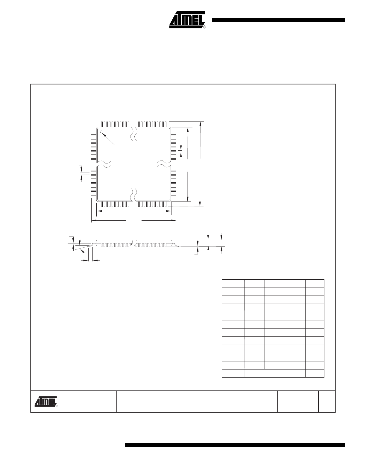
Packaging Information
44A
PIN 1
B
PIN 1 IDENTIFIER
e
E1 E
D1
D
C
0˚~7˚
A1
L
Notes: 1. This package conforms to JEDEC reference MS-026, Variation ACB.
2. Dimensions D1 and E1 do not include mold protrusion. Allowable
protrusion is 0.25 mm per side. Dimensions D1 and E1 are maximum
plastic body size dimensions including mold mismatch.
3. Lead coplanarity is 0.10 mm maximum.
A2 A
SYMBOL
COMMON DIMENSIONS
(Unit of Measure = mm)
MIN
A – – 1.20
A1 0.05 – 0.15
A2 0.95 1.00 1.05
D 11.75 12.00 12.25
D1 9.90 10.00 10.10 Note 2
E 11.75 12.00 12.25
E1 9.90 10.00 10.10 Note 2
B 0.30 – 0.45
C 0.09 – 0.20
L 0.45 – 0.75
e 0.80 TYP
NOM
MAX
NOTE
14
2325 Orchard Parkway
R
San Jose, CA 95131
ATmega162/V
TITLE
44A, 44-lead, 10 x 10 mm Body Size, 1.0 mm Body Thickness,
0.8 mm Lead Pitch, Thin Profile Plastic Quad Flat Package (TQFP)
10/5/2001
DRAWING NO.
44A
2513DS–AVR–04/03
REV.
B
Page 15
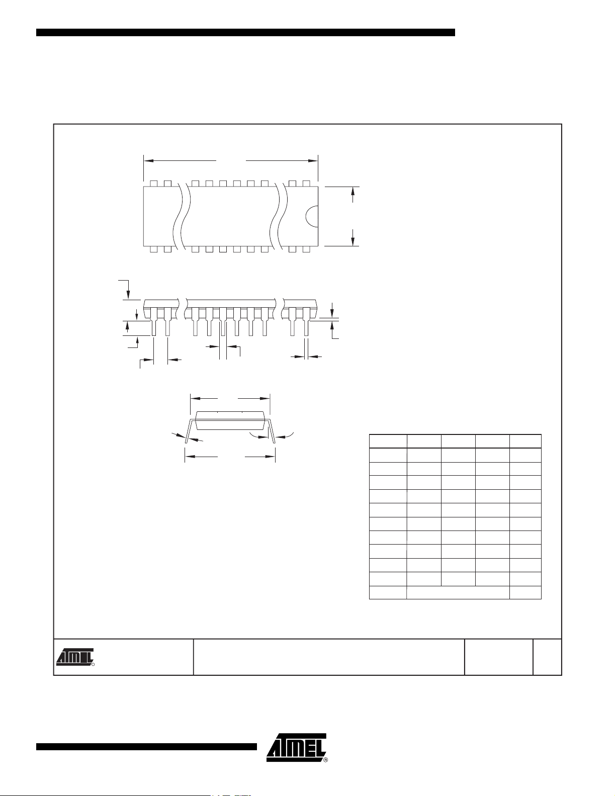
40P6
PIN
1
E1
A1
B
REF
E
B1
C
L
SEATING PLANE
A
ATmega162/V
D
e
0º ~ 15º
eB
Notes: 1. This package conforms to JEDEC reference MS-011, Variation AC.
2. Dimensions D and E1 do not include mold Flash or Protrusion.
Mold Flash or Protrusion shall not exceed 0.25 mm (0.010").
2325 Orchard Parkway
R
San Jose, CA 95131
TITLE
40P6, 40-lead (0.600"/15.24 mm Wide) Plastic Dual
Inline Package (PDIP)
COMMON DIMENSIONS
(Unit of Measure = mm)
SYMBOL
A – – 4.826
A1 0.381 – –
D 52.070 – 52.578 Note 2
E 15.240 – 15.875
E1 13.462 – 13.970 Note 2
B 0.356 – 0.559
B1 1.041 – 1.651
L 3.048 – 3.556
C 0.203 – 0.381
eB 15.494 – 17.526
e 2.540 TYP
MIN
NOM
MAX
DRAWING NO.
40P6
NOTE
09/28/01
REV.
B
2513DS–AVR–04/03
15
Page 16
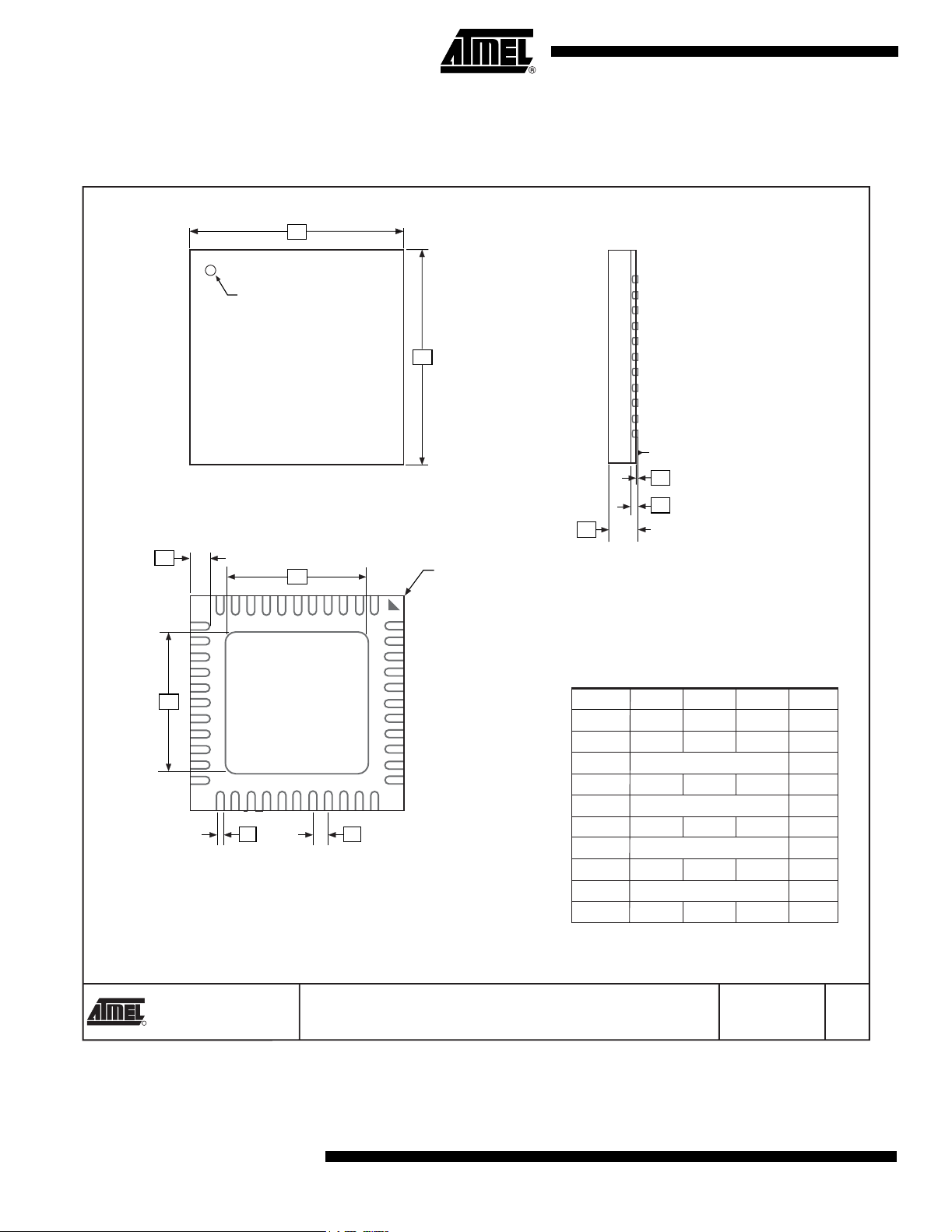
44M1
D
Marked Pin# 1 ID
E
SEATING PLANE
TOP VIEW
L
D2
Pin #1 Corner
E2
b
e
BOTT OM VIEW
Note: JEDEC Standard MO-220, Fig. 1 (SAW Singulation) VKKD-1.
A1
A3
A
SIDE VIEW
COMMON DIMENSIONS
(Unit of Measure = mm)
SYMBOL
A 0.80 0.90 1.00
A1 – 0.02 0.05
A3 0.25 REF
b 0.18 0.23 0.30
D 7.00 BSC
D2 5.00 5.20 5.40
E 7.00 BSC
E2 5.00 5.20 5.40
e 0.50 BSC
L 0.35 0.55 0.75
MIN
NOM
MAX
NOTE
16
2325 Orchard Parkway
R
San Jose, CA 95131
TITLE
ATmega162/V
44M1, 44-pad, 7 x 7 x 1.0 mm Body, Lead Pitch 0.50 mm
Micro Lead Frame Package (MLF)
DRAWING NO.
44M1
2513DS–AVR–04/03
01/15/03
REV.
C
Page 17

ATmega162/V
Data Sheet Change Log for ATmega162
Changes from Rev. 2513A-05/02 to Rev. 2513B-09/02
Changes from Rev. 2513B-09/02 to Rev. 2513C-09/02
Changes from Rev. 2513C-09/02 to Rev. 2513D-04/03
Please note that the referring page numbers in this section are referred to this document. The referring revision in this section are referring to the document revision.
1. Added information for ATmega162U.
Information about ATmega162U included in “Features” on page 1, Table 19,
“BODLEVEL Fuse Coding,” on page 48, and “Ordering Information” on page 13.
1. Canged the Endurance on the Flash to 10,000 Write/Erase Cycles.
1. Updated the “Orderi ng Info rmatio n” on p age 13 and “Packaging Information”
on page 14.
2. Updated “Features” on page 1.
3. Added characterization plots under “ATmega162 Typical Characteristics –
Preliminary Data” on page 273.
4. Added Chip Erase as a first step under “Programm ing the Flash” on pag e 258
and “Programming the EEPROM” on page 260.
5. Changed CAL7, the highest bit in the OSCCAL Reg ister, to a reserved bit on
page 37 and in “Register Summary” on page 7.
6. Changed CPCE to CLKPCE on page 39.
7. Corrected code examples on page 53.
8. Corrected OCn waveforms in Figure 52 on page 118.
9. Various minor Timer1 corrections.
10. Added note under “Filling the Tem porary Bu ffe r (Page L oading)” o n p age 2 22
about writing to the EEPROM durin g an SPM Pa ge Lo ad.
11. Added section “EEPROM Write During Power-down Sleep Mode” on page 22.
12. Added inform ation about PWM sym metry for Timer0 on page 96 and T imer2
on page 145.
13. Updated Table 18 on page 46, Table 20 on page 48, Table 36 on page 75, Table
83 on page 20 3, Table 110 on page 245, Table 113 o n pag e 265, and Table 114
on page 266.
14. Added Figures for “Absolute Maximum Frequency as a function of VCC,
ATmega162” on page 264.
15. Updated Fig ure 29 on pa ge 62, Figure 32 o n page 66 , and Figure 88 on page
208.
2513DS–AVR–04/03
17
Page 18

16. Removed Table 114, “External RC Oscillator, Typical Frequencies
page 265.
17. Updated “Electrical Characteristi cs” on page 262.
(1)
,” on
18
ATmega162/V
2513DS–AVR–04/03
Page 19

Atmel Corporation Atmel Operations
2325 Orchard Park way
San Jose, CA 95131
Tel: 1(408) 4 41-0311
Fax: 1(408) 487-260 0
Regional Headquar ters
Europe
Atmel Sa rl
Route des Ars enau x 41
Case Postale 8 0
CH-1705 Fri bourg
Switzerland
Tel: (41) 26-4 26-55 55
Fax: (41) 26 -426-550 0
Asia
Room 121 9
Chinachem Gold en Plaza
77 Mody Ro ad Tsims hatsu i
East Kowloon
Hong Kong
Tel: (852) 27 21-9778
Fax: (852) 2 722-136 9
Japan
9F, Tonetsu Sh inkaw a Bl dg.
1-24-8 Shi nkawa
Chuo-ku, Tok yo 10 4-0033
Japan
Tel: (81) 3-35 23-35 51
Fax: (81) 3-3 523-758 1
Memory
2325 Orch ard Parkw ay
San Jose, C A 95131
Tel: 1(408 ) 441-031 1
Fax: 1(408) 43 6-43 14
Microcontrollers
2325 Orch ard Parkw ay
San Jose, C A 95131
Tel: 1(408 ) 441-031 1
Fax: 1(408) 43 6-43 14
La Chantrer ie
BP 70602
44306 Na ntes Cede x 3, Fra nce
Tel: (33) 2-4 0-18 -18-18
Fax: (33) 2-40-18-19-60
ASIC/ASSP/Smart Cards
Zone In dustrielle
13106 Rousse t Ced ex, France
Tel: (33) 4-4 2-53 -60-00
Fax: (33) 4-42-53-60-01
1150 East C heyenn e Mtn. Blvd.
Colorado Sp rings, CO 8 0906
Tel: 1(719 ) 576-330 0
Fax: 1(719) 54 0-17 59
Scottish Enterprise Technology Park
Maxwell Building
East Kilbrid e G7 5 0QR, S cotlan d
Tel: (44) 13 55-803- 000
Fax: (44) 1355 -242 -743
RF/Automotive
Theresienstrasse 2
Postfach 3535
74025 Heilbr onn, Ge rmany
Tel: (49) 71-31-67-0
Fax: (49) 71 -31-67- 2340
1150 East Ch eyenne M tn. B lvd.
Colorado Spr ings, CO 80 906
Tel: 1(719) 57 6-3300
Fax: 1(719) 540-1759
Biometrics/Imaging/Hi-Rel MPU/
High Speed Converters/RF Datacom
Avenue de R ocheplei ne
BP 123
38521 Saint- Egreve Cedex, France
Tel: (33) 4-76-58-30-00
Fax: (33) 4-7 6-58-3 4-80
e-mail
literature@at mel.com
Web Site
http://www.atmel.com
Disclaimer: Atmel Corporation makes no warranty for the use of its products, other than those expressly contained in the Company’s standard
warranty which is detailed in Atmel’s Terms and Conditions located on the Company’s web site. The Company assumes no responsibility for any
errors which may appear in this document , reserves the right to change devices or specifications detailed herein at any time without notice, and
does no t make any com mitment to u pdate the informat ion contai ned herei n. No licen ses to paten ts or othe r intellec tual proper ty of Atmel are
granted by th e Com pany in conn ecti on w ith t he sale of A tme l pr oduc ts, exp ressl y or by im pli catio n. Atme l’s pro duct s ar e no t aut hori zed for use
as critical components in life support devices or systems.
© Atmel Corporation 2003. All rights reserved. Atmel® and combinations thereof, AVR®, and AVR Studio
are the r egistered trademar ks of Atmel Cor poratio n or its sub sidiarie s. Micros oft®, Window s®, Window s NT®,
and Win dows XP
may be t he trademar k s of others.
®
are the r egistered trademark s of Microso ft Corpor ation. Othe r terms a nd product names
®
Printe d on rec ycled pape r.
2513DS–AVR–04/03 0M
 Loading...