

Page 1

Atmel 8-bit AVR Microcontroller with 512/1024 Bytes In-System
Programmable Flash
ATtiny4 / ATtiny5 / ATtiny9 / ATiny10
DATASHEET SUMMARY
Introduction
The Atmel® ATtiny4/5/9/10 is a low-power CMOS 8-bit microcontroller based
on the AVR® enhanced RISC architecture. By executing powerful
instructions in a single clock cycle, the ATtiny4/5/9/10 achieves throughputs
close to 1 MIPS per MHz. This empowers system designer to optimize the
device for power consumption versus processing speed.
Feature
• High Performance, Low Power AVR® 8-Bit Microcontroller
• Advanced RISC Architecture
– 54 Powerful Instructions
– Most Single Clock Cycle Execution
– 16 x 8 General Purpose Working Registers
– Fully Static Operation
– Up to 12 MIPS Throughput at 12 MHz
• Non-volatile Program and Data Memories
– 512/1024 Bytes of In-System Programmable Flash Program
Memory
– 32 Bytes Internal SRAM
– Flash Write/Erase Cycles: 10,000
– Data Retention: 20 Years at 85°C / 100 Years at 25°C
• Peripheral Features
– QTouch® Library Support for Capacitive Touch Sensing (1
Channel)
– One 16-bit Timer/Counter with Prescaler and Two PWM
Channels
– Programmable Watchdog Timer with Separate On-chip Oscillator
– 4-channel, 8-bit Analog to Digital Converter (ATtiny5/10, only)
– On-chip Analog Comparator
• Special Microcontroller Features
– In-System Programmable (at 5V, only)
Atmel-8127H-ATiny4/ ATiny5 /ATiny9/ ATiny10_Datasheet_Summary-11/2016
Page 2

– External and Internal Interrupt Sources
– Low Power Idle, ADC Noise Reduction, and Power-down Modes
– Enhanced Power-on Reset Circuit
– Programmable Supply Voltage Level Monitor with Interrupt and Reset
– Internal Calibrated Oscillator
• I/O and Packages
– Four Programmable I/O Lines
– 6-pin SOT and 8-pad UDFN
• Operating Voltage:
– 1.8 - 5.5V
• Programming Voltage:
– 5V
• Speed Grade:
– 0 - 4 MHz @ 1.8 - 5.5V
– 0 - 8 MHz @ 2.7 - 5.5V
– 0 - 12 MHz @ 4.5 - 5.5V
• Industrial and Extended Temperature Ranges
• Low Power Consumption
– Active Mode:
• 200μA at 1MHz and 1.8V
Idle Mode:
• 25μA at 1MHz and 1.8V
– Power-down Mode:
• <0.1μA at 1.8V
Atmel ATtiny4 / ATtiny5 / ATtiny9 / ATiny10 [DATASHEET]
Atmel-8127H-ATiny4/ ATiny5 /ATiny9/ ATiny10_Datasheet_Summary-11/2016
2
Page 3

Table of Contents
Introduction......................................................................................................................1
Feature............................................................................................................................ 1
1. Pin Configurations..................................................................................................... 4
1.1. Pin Descriptions............................................................................................................................4
2. Ordering Information..................................................................................................5
2.1. ATtiny4..........................................................................................................................................5
2.2. ATtiny5..........................................................................................................................................6
2.3. ATtiny9..........................................................................................................................................7
2.4. ATtiny10........................................................................................................................................8
3. Overview....................................................................................................................9
3.1. Block Diagram..............................................................................................................................9
3.2. Comparison of ATtiny4, ATtiny5, ATtiny9 and ATtiny10............................................................. 10
4. General Information................................................................................................. 11
4.1. Resources...................................................................................................................................11
4.2. Data Retention............................................................................................................................11
4.3. About Code Examples................................................................................................................11
4.4. Capacitive Touch Sensing.......................................................................................................... 11
5. Packaging Information.............................................................................................12
5.1. 6ST1...........................................................................................................................................12
5.2. 8MA4..........................................................................................................................................13
6. Errata.......................................................................................................................14
6.1. ATtiny4........................................................................................................................................14
6.2. ATtiny5........................................................................................................................................14
6.3. ATtiny9........................................................................................................................................15
6.4. ATtiny10......................................................................................................................................16
Page 4
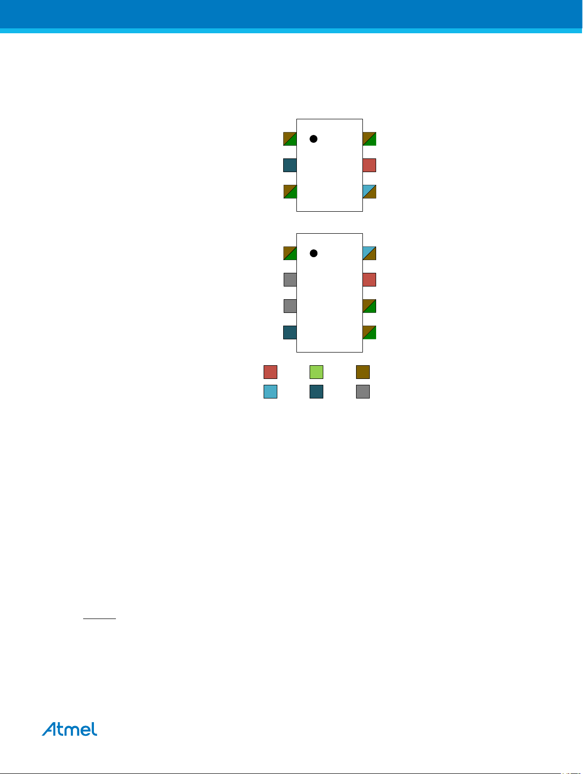
1. Pin Configurations
1
2
3 4
6
5 VCC
GND
PB2 (T0/CLKO/PCINT2/INT0/ADC2)
PB3 (RESET/PCINT3/ADC3)
SOT-23
(PCINT0/TPIDATA /OC0A/ADC0/AIN0) PB0
(PCINT1/TPICLK/CLKI/ICP0/OC0B/ADC1/AIN1) PB1
1
2
3
4
8
7
6
5
VCC
GND
PB3 (RESET/PCINT3/ADC3)
PB0 (AIN0/ADC0/OC0A/TPIDATA /PCINT0)
Power
Clock
Digital
GND
Analog
UDFN
PB2 (T0/CLKO/PCINT2/INT0/ADC2)(PCINT1/TPICLK/CLKI/ICP0/OC0B/ADC1/AIN1) PB1
NC
NC
NC
Figure 1-1. Pinout of ATtiny4/5/9/10
1.1. Pin Descriptions
1.1.1. VCC
Digital supply voltage.
1.1.2. GND
1.1.3. Port B (PB[3:0])
1.1.4. RESET
Ground.
This is a 4-bit, bi-directional I/O port with internal pull-up resistors, individually selectable for each bit. The
output buffers have symmetrical drive characteristics, with both high sink and source capability. As inputs,
the port pins that are externally pulled low will source current if pull-up resistors are activated. Port pins
are tri-stated when a reset condition becomes active, even if the clock is not running.
Reset input. A low level on this pin for longer than the minimum pulse length will generate a reset, even if
the clock is not running and provided the reset pin has not been disabled. The minimum pulse length is
given in System and Reset Characteristics of Electrical Characteristics. Shorter pulses are not
guaranteed to generate a reset.
The reset pin can also be used as a (weak) I/O pin.
Atmel ATtiny4 / ATtiny5 / ATtiny9 / ATiny10 [DATASHEET]
Atmel-8127H-ATiny4/ ATiny5 /ATiny9/ ATiny10_Datasheet_Summary-11/2016
4
Page 5

2. Ordering Information
2.1. ATtiny4
Supply Voltage Speed
1.8 – 5.5V 12MHz
10MHz
(1)
Temperature Package
Industrial
(-40°C to 85°C)
(4)
Extended
(-40°C to 125°C)
(8)
6ST1 ATTINY4-TSUR
8MA4 ATTINY4-MAHR
6ST1 ATTINY4-TSFR
(2)
Ordering Code
ATTINY4-TSHR
ATTINY4-TS8R
(3)
(5)
(6)(7)
(7)
(5)
(6)(7)
Note:
1. For speed vs. supply voltage, see section Speed.
2. All packages are Pb-free, halide-free and fully green and they comply with the European directive
for Restriction of Hazardous Substances (RoHS). NiPdAu finish.
3. Tape and reel.
4. Can also be supplied in wafer form. Contact your local sales office for ordering information and
minimum quantities.
5. Marking details:
– Top mark 1st line: ddddTY
– Top mark 2nd line: wwxxx
dddd= device, special code
T= Type
Y= Year last digit
ww= calendar workweek
xxx = trace code
6. Not recommended for new designs.TPUBSTINY-216
7. Top/bottom markings:
– Top: T4x, where x = die revision
– Bottom: zHzzz or z8zzz, where H = (-40°C to 85°C), and 8 = (-40°C to 125°C)
8. For typical and Electrical characteristics for this device please consult Appendix A, ATtiny4/5/9/10
Specification at 125°C.
Table 2-1. Package Type
6ST1 6-lead, 2.90 x 1.60 mm Plastic Small Outline Package (SOT23)
8MA4 8-pad, 2 x 2 x 0.6 mm Plastic Ultra Thin Dual Flat No Lead (UDFN)
Atmel ATtiny4 / ATtiny5 / ATtiny9 / ATiny10 [DATASHEET]
Atmel-8127H-ATiny4/ ATiny5 /ATiny9/ ATiny10_Datasheet_Summary-11/2016
5
Page 6

2.2. ATtiny5
Supply Voltage Speed
1.8 – 5.5V 12MHz
10MHz
(1)
Temperature Package
Industrial
(-40°C to 85°C)
(4)
Extended
(-40°C to 125°C)
(8)
6ST1 ATTINY5-TSUR
8MA4 ATTINY5-MAHR
6ST1 ATTINY5-TSFR
(2)
Ordering Code
ATTINY5-TSHR
ATTINY5-TS8R
(3)
(5)
(6)(7)
(7)
(5)
(6)(7)
Note:
1. For speed vs. supply voltage, see section Speed.
2. All packages are Pb-free, halide-free and fully green and they comply with the European directive
for Restriction of Hazardous Substances (RoHS). NiPdAu finish.
3. Tape and reel.
4. Can also be supplied in wafer form. Contact your local sales office for ordering information and
minimum quantities.
5. Marking details:
– Top mark 1st line: ddddTY
– Top mark 2nd line: wwxxx
dddd= device, special code
T= Type
Y= Year last digit
ww= calendar workweek
xxx = trace code
6. Not recommended for new designs.TPUBSTINY-216
7. Top/bottomside markings:
– Top: T5x, where x = die revision
– Bottom: zHzzz or z8zzz, where H = (-40°C to 85°C), and 8 = (-40°C to 125°C)
8. For typical and Electrical characteristics for this device please consult Appendix A, ATtiny4/5/9/10
Specification at 125°C.
Table 2-2. Package Type
6ST1 6-lead, 2.90 x 1.60 mm Plastic Small Outline Package (SOT23)
8MA4 8-pad, 2 x 2 x 0.6 mm Plastic Ultra Thin Dual Flat No Lead (UDFN)
Atmel ATtiny4 / ATtiny5 / ATtiny9 / ATiny10 [DATASHEET]
Atmel-8127H-ATiny4/ ATiny5 /ATiny9/ ATiny10_Datasheet_Summary-11/2016
6
Page 7

2.3. ATtiny9
Supply Voltage Speed
1.8 – 5.5V 12MHz
10MHz
(1)
Temperature Package
Industrial
(-40°C to 85°C)
(4)
Extended
(-40°C to 125°C)
(8)
6ST1 ATTINY9-TSUR
8MA4 ATTINY9-MAHR
6ST1 ATTINY9-TSFR
(2)
Ordering Code
ATTINY9-TSHR
ATTINY9-TS8R
(3)
(5)
(6)(7)
(7)
(5)
(6)(7)
Note:
1. For speed vs. supply voltage, see section Speed.
2. All packages are Pb-free, halide-free and fully green and they comply with the European directive
for Restriction of Hazardous Substances (RoHS). NiPdAu finish.
3. Tape and reel.
4. Can also be supplied in wafer form. Contact your local sales office for ordering information and
minimum quantities.
5. Marking details:
– Top mark 1st line: ddddTY
– Top mark 2nd line: wwxxx
dddd= device, special code
T= Type
Y= Year last digit
ww= calendar workweek
xxx = trace code
6. Not recommended for new designs.TPUBSTINY-216
7. Top/bottomside markings:
– Top: T9x, where x = die revision
– Bottom: zHzzz or z8zzz, where H = (-40°C to 85°C), and 8 = (-40°C to 125°C)
8. For typical and Electrical characteristics for this device please consult Appendix A, ATtiny4/5/9/10
Specification at 125°C.
Table 2-3. Package Type
6ST1 6-lead, 2.90 x 1.60 mm Plastic Small Outline Package (SOT23)
8MA4 8-pad, 2 x 2 x 0.6 mm Plastic Ultra Thin Dual Flat No Lead (UDFN)
Atmel ATtiny4 / ATtiny5 / ATtiny9 / ATiny10 [DATASHEET]
Atmel-8127H-ATiny4/ ATiny5 /ATiny9/ ATiny10_Datasheet_Summary-11/2016
7
Page 8

2.4. ATtiny10
Supply Voltage Speed
1.8 – 5.5V 12MHz
10MHz
(1)
Temperature Package
Industrial
(-40°C to 85°C)
(4)
Extended
(-40°C to 125°C)
(8)
6ST1 ATTINY10-TSUR
8MA4 ATTINY10-MAHR
6ST1 ATTINY10-TSFR
(2)
Ordering Code
ATTINY10-TSHR
ATTINY10-TS8R
(3)
(5)
(6)(7)
(7)
(5)
(6)(7)
Note:
1. For speed vs. supply voltage, see section Speed.
2. All packages are Pb-free, halide-free and fully green and they comply with the European directive
for Restriction of Hazardous Substances (RoHS). NiPdAu finish.
3. Tape and reel.
4. Can also be supplied in wafer form. Contact your local sales office for ordering information and
minimum quantities.
5. Marking details:
– Top mark 1st line: ddddTY
– Top mark 2nd line: wwxxx
dddd= device, special code
T= Type
Y= Year last digit
ww= calendar workweek
xxx = trace code
6. Not recommended for new designs.TPUBSTINY-216
7. Top/bottomside markings:
– Top: T10x, where x = die revision
– Bottom: zHzzz or z8zzz, where H = (-40°C to 85°C), and 8 = (-40°C to 125°C)
8. For typical and Electrical characteristics for this device please consult Appendix A, ATtiny4/5/9/10
Specification at 125°C.
Table 2-4. Package Type
6ST1 6-lead, 2.90 x 1.60 mm Plastic Small Outline Package (SOT23)
8MA4 8-pad, 2 x 2 x 0.6 mm Plastic Ultra Thin Dual Flat No Lead (UDFN)
Atmel ATtiny4 / ATtiny5 / ATtiny9 / ATiny10 [DATASHEET]
Atmel-8127H-ATiny4/ ATiny5 /ATiny9/ ATiny10_Datasheet_Summary-11/2016
8
Page 9
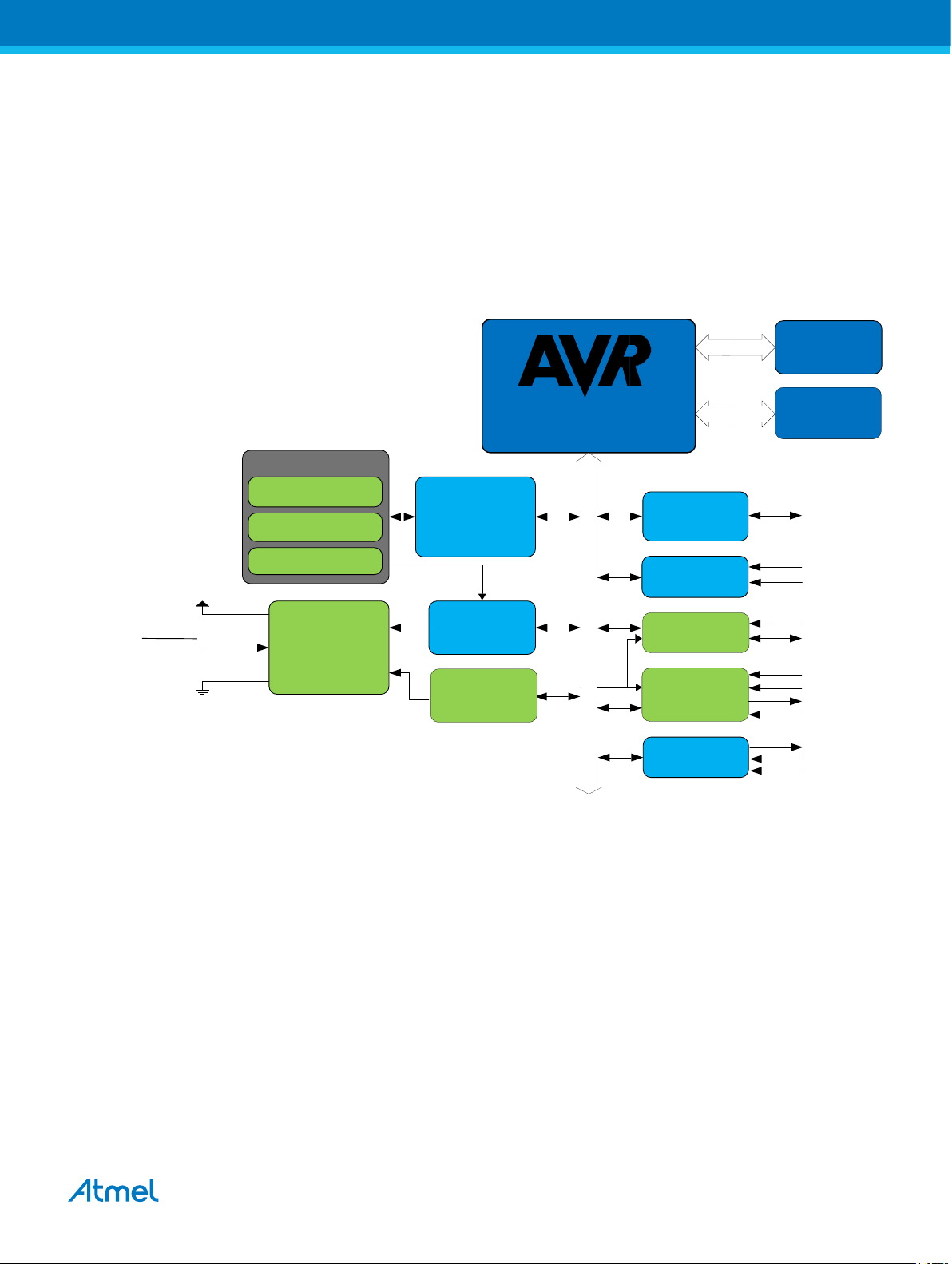
3. Overview
This device is low-power CMOS 8-bit microcontrollers based on the compact AVR enhanced RISC
architecture. By executing powerful instructions in a single clock cycle, the device achieve throughputs
approaching 1 MIPS per MHz, allowing the system designer to optimize power consumption versus
processing speed.
3.1. Block Diagram
Figure 3-1. Block Diagram
SRAM
Vcc
RESET
GND
3.1.1. Description
The AVR core combines a rich instruction set with 16 general purpose working registers and system
registers. All registers are directly connected to the Arithmetic Logic Unit (ALU), allowing two independent
registers to be accessed in one single instruction executed in one clock cycle. The resulting architecture
is compact and code efficient while achieving throughputs up to ten times faster than conventional CISC
microcontrollers.
Clock generation
8MHz Calib Osc
External clock
128 kHz Internal Osc
Power
Supervision
POR & RESET
Power
management
and clock
control
Watchdog
Timer
Internal
Reference
CPU
D
A
T
A
B
U
S
I/O
PORTS
Interrupt
ADC
AC
TC 0
(16-bit)
FLASH
PB[3:0]
PCINT[3:0]
INT0
ADC[7:0]
Vcc
AIN0
AIN1
ACO
ADCMUX
OC0A/B
T0
ICP0
This device provides the following features: 512/1024 byte of In-System Programmable Flash, 32 bytes of
SRAM, four general purpose I/O lines, 16 general purpose working registers, a 16-bit timer/counter with
two PWM channels, internal and external interrupts, a programmable watchdog timer with internal
oscillator, an internal calibrated oscillator, and four software selectable power saving modes. ATtiny5/10
are also equipped with a four-channel and 8-bit Analog to Digital Converter (ADC).
Idle mode stops the CPU while allowing the SRAM, timer/counter, ADC (ATtiny5/10, only), analog
comparator, and interrupt system to continue functioning. ADC Noise Reduction mode minimizes
switching noise during ADC conversions by stopping the CPU and all I/O modules except the ADC. In
Power-down mode registers keep their contents and all chip functions are disabled until the next interrupt
Atmel ATtiny4 / ATtiny5 / ATtiny9 / ATiny10 [DATASHEET]
Atmel-8127H-ATiny4/ ATiny5 /ATiny9/ ATiny10_Datasheet_Summary-11/2016
9
Page 10

or hardware reset. In Standby mode, the oscillator is running while the rest of the device is sleeping,
allowing very fast start-up combined with low power consumption.
The device is manufactured using Atmel’s high density Non-Volatile Memory (NVM) technology. The onchip, in-system programmable Flash allows program memory to be re-programmed in-system by a
conventional, non-volatile memory programmer.
The ATtiny4/5/9/10AVR are supported by a suite of program and system development tools, including
macro assemblers and evaluation kits.
3.2. Comparison of ATtiny4, ATtiny5, ATtiny9 and ATtiny10
A comparison of the devices is shown in the table below.
Table 3-1. Differences between ATtiny4, ATtiny5, ATtiny9 and ATtiny10
Device Flash ADC Signature
ATtiny4 512 bytes No 0x1E 0x8F 0x0A
ATtiny5 512 bytes Yes 0x1E 0x8F 0x09
ATtiny9 1024 bytes No 0x1E 0x90 0x08
ATtiny10 1024 bytes Yes 0x1E 0x90 0x03
Atmel ATtiny4 / ATtiny5 / ATtiny9 / ATiny10 [DATASHEET]
Atmel-8127H-ATiny4/ ATiny5 /ATiny9/ ATiny10_Datasheet_Summary-11/2016
10
Page 11

4. General Information
4.1. Resources
A comprehensive set of development tools, application notes, and datasheets are available for download
on http://www.atmel.com/avr.
4.2. Data Retention
Reliability Qualification results show that the projected data retention failure rate is much less than 1 PPM
over 20 years at 85°C or 100 years at 25°C.
4.3. About Code Examples
This documentation contains simple code examples that briefly show how to use various parts of the
device. These code examples assume that the part specific header file is included before compilation. Be
aware that not all C compiler vendors include bit definitions in the header files and interrupt handling in C
is compiler dependent. Confirm with the C compiler documentation for more details.
For I/O Registers located in extended I/O map, “IN”, “OUT”, “SBIS”, “SBIC”, “CBI”, and “SBI” instructions
must be replaced with instructions that allow access to extended I/O. Typically “LDS” and “STS”
combined with “SBRS”, “SBRC”, “SBR”, and “CBR”.
4.4. Capacitive Touch Sensing
4.4.1. QTouch Library
The Atmel® QTouch® Library provides a simple to use solution to realize touch sensitive interfaces on
most Atmel AVR® microcontrollers. The QTouch Library includes support for the Atmel QTouch and Atmel
QMatrix® acquisition methods.
Touch sensing can be added to any application by linking the appropriate Atmel QTouch Library for the
AVR Microcontroller. This is done by using a simple set of APIs to define the touch channels and sensors,
and then calling the touch sensing API’s to retrieve the channel information and determine the touch
sensor states.
The QTouch Library is FREE and downloadable from the Atmel website at the following location: http://
www.atmel.com/technologies/touch/. For implementation details and other information, refer to the Atmel
QTouch Library User Guide - also available for download from the Atmel website.
Atmel ATtiny4 / ATtiny5 / ATtiny9 / ATiny10 [DATASHEET]
Atmel-8127H-ATiny4/ ATiny5 /ATiny9/ ATiny10_Datasheet_Summary-11/2016
11
Page 12
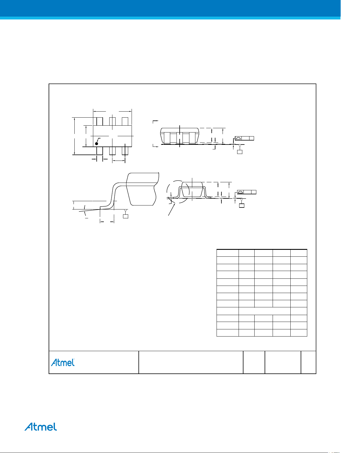
5. Packaging Information
TITLE
DRAWING NO. GPC
REV.
Pac kage Drawin g Co ntac t:
pa ckag e drawing s @ a tmel.com
6S T1TAQ A
6S T1, 6-lead, 2.90 x 1.60 mm Plastic Sm all Outline
Package (SOT23)
MAX
NOTE
SYMBOL
MIN
NOM
COMMON DIMENSIONS
(Unit of Mea s ure = mm)
A – – 1 .45
A1 0 – 0.1 5
A2 0.90 – 1 .30
D 2.80 2 .90 3.0 0 2
E 2 .6 0 2.8 0 3.00
E1 1.50 1.60 1 .7 5
L 0 .3 0 0.4 5 0.55
e 0.9 5 BS C
b 0.30 – 0.50 3
c 0 .09 – 0 .2 0
θ 0° – 8°
Notes: 1. Th is package is compliant with JEDEC spe cif cation MO-178 Variation AB
2. Dimen sion D doe s not include mo ld Flash, protrusions or ga te burrs.
Mold Flash , protrustion or ga te burrs shall not exceed 0.25 mm per en d.
3. Dimen sion b doe s no t includ e dambar protrusion . Allowab le damb ar
protrusion sha ll no t cau se the lead widt h to excee d the maximum
b dimen sion by more than 0.08 mm
4. Die is facing down after trim/form.
6/30/0 8
Side View
E E1
D
e
A2
A
A1
C
C
0.10
0.25
L
O
A2
A
A1
C
C
0.10
A
A
SEE VIEW B
C
SEATING PLANE
SEATING PLANE
SEATING PLANE
c
b
Pin #1 ID
1
6
2
3
5
4
To p View
View B
View A-A
5.1. 6ST1
Figure 5-1. 6ST1
Atmel ATtiny4 / ATtiny5 / ATtiny9 / ATiny10 [DATASHEET]
Atmel-8127H-ATiny4/ ATiny5 /ATiny9/ ATiny10_Datasheet_Summary-11/2016
12
Page 13
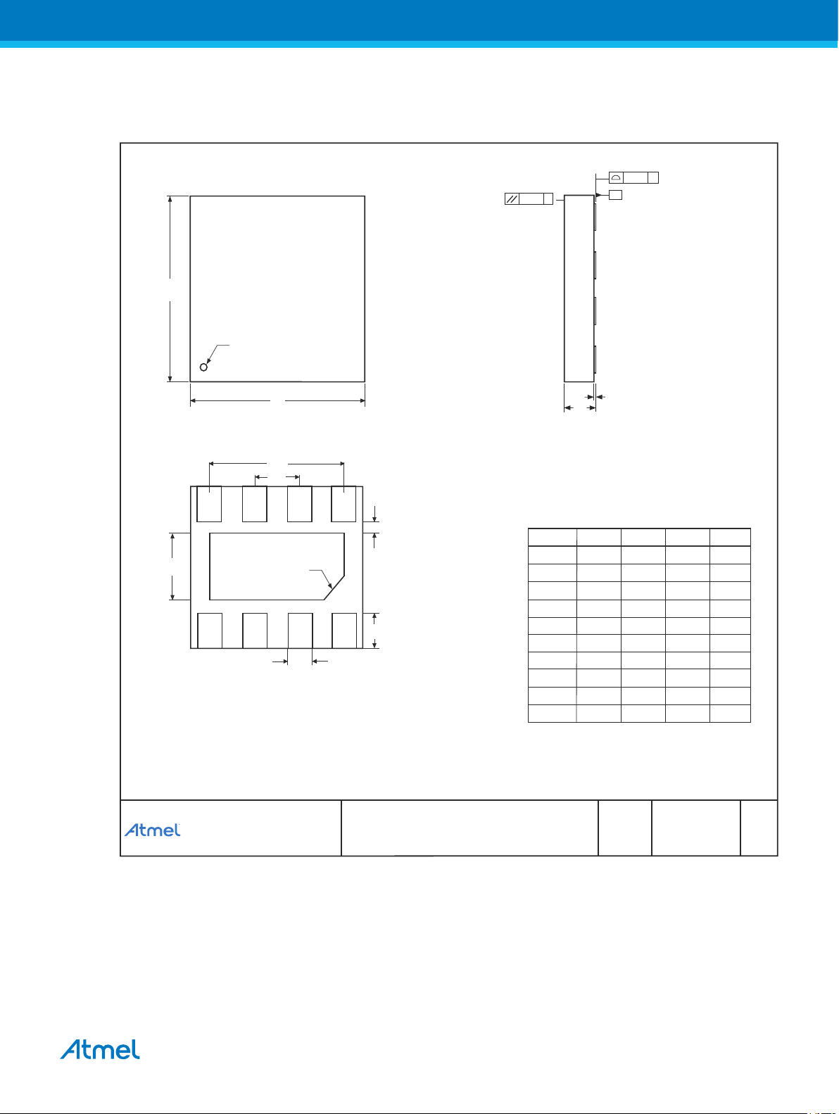
5.2. 8MA4
TITLE
DRAWING NO.GPC
REV.
Pac kage Drawin g Co ntac t:
pa ckag e drawing s @ a tmel.com
8MA4YAG A
8PAD, 2x2x 0.6 mm bo dy, 0.5 mm pitc h,
0.9x1.5 mm ex pos ed pad , Sa w s ing ulate d
Thermally e nha nc ed plas tic ultra thin dual flat
no lead pac kage (UDFN/USON)
12/17 /09
COMMON DIMENS IONS
(Unit of Mea s ure = mm )
SYMBOL
MIN
NOM
MAX
NOTE
A – – 0.6 0
A1 0.0 0 – 0.0 5
b 0. 20 – 0.30
D 1 .95 2.0 0 2 .05
D2 1.40 1.5 0 1.60
E 1 .95 2.0 0 2 .05
E 2 0 .80 0.9 0 1.00
e – 0.50 –
L 0 .2 0 0.3 0 0 .40
K 0 .20 – –
TOP VIEW
BOTTOM VIEW
Note :
1. ALL DIMENS IONS ARE IN mm. ANGLES IN DEGR EES .
2. C OPLANARITY APPLIES TO THE EXPOSED PAD AS WELL AS THE
TERMINALS COPLANARITY SHALL NOT EXCEED 0.05 mm.
3. WARPAGE SHALL NOT EXCEED 0.05 mm.
4. REFER JEDEC MO-236/MO-252
Pin 1 ID
E
D
D2
1 2 3 4
8 7 6 5
E2
b
14
8
5
e
K
L
0.0 5
SIDE VIEW
A1
A
c
c
0.0 5 c
8x
C0.2
Figure 5-2. 8MA4
Atmel ATtiny4 / ATtiny5 / ATtiny9 / ATiny10 [DATASHEET]
Atmel-8127H-ATiny4/ ATiny5 /ATiny9/ ATiny10_Datasheet_Summary-11/2016
13
Page 14

6. Errata
6.1. ATtiny4
6.1.1. Rev. E
• Programming Lock Bits
1. Programming Lock Bits
Programming Lock Bits to a lock mode equal or lower than the current causes one word of Flash to be
corrupted. The location of the corruption is random.
Problem Fix / Workaround
When programming Lock Bits, make sure lock mode is not set to present, or lower levels.
6.1.2. Rev. D
• ESD HBM (ESD STM 5.1) level ±1000V
• Programming Lock Bits
1. ESD HBM (ESD STM 5.1) level ±1000V
The device meets ESD HBM (ESD STM 5.1) level ±1000V.
Problem Fix / Workaround
Always use proper ESD protection measures (Class 1C) when handling integrated circuits before and
during assembly.
2. Programming Lock Bits
Programming Lock Bits to a lock mode equal or lower than the current causes one word of Flash to be
corrupted. The location of the corruption is random.
Problem Fix / Workaround
When programming Lock Bits, make sure lock mode is not set to present, or lower levels.
6.1.3. Rev. A – C
Not sampled.
6.2. ATtiny5
6.2.1. Rev. E
• Programming Lock Bits
1. Programming Lock Bits
Programming Lock Bits to a lock mode equal or lower than the current causes one word of Flash to be
corrupted. The location of the corruption is random.
Problem Fix / Workaround
When programming Lock Bits, make sure lock mode is not set to present, or lower levels.
Atmel ATtiny4 / ATtiny5 / ATtiny9 / ATiny10 [DATASHEET]
Atmel-8127H-ATiny4/ ATiny5 /ATiny9/ ATiny10_Datasheet_Summary-11/2016
14
Page 15

6.2.2. Rev. D
• ESD HBM (ESD STM 5.1) level ±1000V
• Programming Lock Bits
1. ESD HBM (ESD STM 5.1) level ±1000V
The device meets ESD HBM (ESD STM 5.1) level ±1000V.
Problem Fix / Workaround
Always use proper ESD protection measures (Class 1C) when handling integrated circuits before and
during assembly.
2. Programming Lock Bits
Programming Lock Bits to a lock mode equal or lower than the current causes one word of Flash to be
corrupted. The location of the corruption is random.
Problem Fix / Workaround
When programming Lock Bits, make sure lock mode is not set to present, or lower levels.
6.2.3. Rev. A – C
Not sampled.
6.3. ATtiny9
6.3.1. Rev. E
• Programming Lock Bits
1. Programming Lock Bits
Programming Lock Bits to a lock mode equal or lower than the current causes one word of Flash to be
corrupted. The location of the corruption is random.
Problem Fix / Workaround
When programming Lock Bits, make sure lock mode is not set to present, or lower levels.
6.3.2. Rev. D
• ESD HBM (ESD STM 5.1) level ±1000V
• Programming Lock Bits
1. ESD HBM (ESD STM 5.1) level ±1000V
The device meets ESD HBM (ESD STM 5.1) level ±1000V.
Problem Fix / Workaround
Always use proper ESD protection measures (Class 1C) when handling integrated circuits before and
during assembly.
2. Programming Lock Bits
Programming Lock Bits to a lock mode equal or lower than the current causes one word of Flash to be
corrupted. The location of the corruption is random.
Problem Fix / Workaround
When programming Lock Bits, make sure lock mode is not set to present, or lower levels.
Atmel ATtiny4 / ATtiny5 / ATtiny9 / ATiny10 [DATASHEET]
Atmel-8127H-ATiny4/ ATiny5 /ATiny9/ ATiny10_Datasheet_Summary-11/2016
15
Page 16

6.3.3. Rev. A – C
Not sampled.
6.4. ATtiny10
6.4.1. Rev. E
• Programming Lock Bits
1. Programming Lock Bits
Programming Lock Bits to a lock mode equal or lower than the current causes one word of Flash to be
corrupted. The location of the corruption is random.
Problem Fix / Workaround
When programming Lock Bits, make sure lock mode is not set to present, or lower levels.
6.4.2. Rev. C – D
• ESD HBM (ESD STM 5.1) level ±1000V
• Programming Lock Bits
1. ESD HBM (ESD STM 5.1) level ±1000V
The device meets ESD HBM (ESD STM 5.1) level ±1000V.
Problem Fix / Workaround
Always use proper ESD protection measures (Class 1C) when handling integrated circuits before and
during assembly.
2. Programming Lock Bits
Programming Lock Bits to a lock mode equal or lower than the current causes one word of Flash to be
corrupted. The location of the corruption is random.
Problem Fix / Workaround
When programming Lock Bits, make sure lock mode is not set to present, or lower levels.
6.4.3. Rev. A – B
Not sampled.
Atmel ATtiny4 / ATtiny5 / ATtiny9 / ATiny10 [DATASHEET]
Atmel-8127H-ATiny4/ ATiny5 /ATiny9/ ATiny10_Datasheet_Summary-11/2016
16
Page 17

Atmel Corporation 1600 Technology Drive, San Jose, CA 95110 USA T: (+1)(408) 441.0311 F: (+1)(408) 436.4200 | www.atmel.com
©
2016 Atmel Corporation. / Rev.: Atmel-8127H-ATiny4/ ATiny5 /ATiny9/ ATiny10_Datasheet_Summary-11/2016
Atmel®, Atmel logo and combinations thereof, Enabling Unlimited Possibilities®, AVR® and others are registered trademarks or trademarks of Atmel Corporation in
U.S. and other countries. Other terms and product names may be trademarks of others.
DISCLAIMER: The information in this document is provided in connection with Atmel products. No license, express or implied, by estoppel or otherwise, to any
intellectual property right is granted by this document or in connection with the sale of Atmel products. EXCEPT AS SET FORTH IN THE ATMEL TERMS AND
CONDITIONS OF SALES LOCATED ON THE ATMEL WEBSITE, ATMEL ASSUMES NO LIABILITY WHATSOEVER AND DISCLAIMS ANY EXPRESS, IMPLIED
OR STATUTORY WARRANTY RELATING TO ITS PRODUCTS INCLUDING, BUT NOT LIMITED TO, THE IMPLIED WARRANTY OF MERCHANTABILITY,
FITNESS FOR A PARTICULAR PURPOSE, OR NON-INFRINGEMENT. IN NO EVENT SHALL ATMEL BE LIABLE FOR ANY DIRECT, INDIRECT,
CONSEQUENTIAL, PUNITIVE, SPECIAL OR INCIDENTAL DAMAGES (INCLUDING, WITHOUT LIMITATION, DAMAGES FOR LOSS AND PROFITS, BUSINESS
INTERRUPTION, OR LOSS OF INFORMATION) ARISING OUT OF THE USE OR INABILITY TO USE THIS DOCUMENT, EVEN IF ATMEL HAS BEEN ADVISED
OF THE POSSIBILITY OF SUCH DAMAGES. Atmel makes no representations or warranties with respect to the accuracy or completeness of the contents of this
document and reserves the right to make changes to specifications and products descriptions at any time without notice. Atmel does not make any commitment to
update the information contained herein. Unless specifically provided otherwise, Atmel products are not suitable for, and shall not be used in, automotive
applications. Atmel products are not intended, authorized, or warranted for use as components in applications intended to support or sustain life.
SAFETY-CRITICAL, MILITARY, AND AUTOMOTIVE APPLICATIONS DISCLAIMER: Atmel products are not designed for and will not be used in connection with any
applications where the failure of such products would reasonably be expected to result in significant personal injury or death (“Safety-Critical Applications”) without
an Atmel officer's specific written consent. Safety-Critical Applications include, without limitation, life support devices and systems, equipment or systems for the
operation of nuclear facilities and weapons systems. Atmel products are not designed nor intended for use in military or aerospace applications or environments
unless specifically designated by Atmel as military-grade. Atmel products are not designed nor intended for use in automotive applications unless specifically
designated by Atmel as automotive-grade.
 Loading...