

ATMEL ATF22V10C-7XC, ATF22V10C-7SC, ATF22V10C-7PC, ATF22V10C-7JC, ATF22V10C-5JC Datasheet
...
Features
Industry Standard Architecture
•
Low Cost Easy-to-Use Software Tools
High Speed Electrically Erasable Programmable Logic Devices
•
5 ns Maximum Pin-to-Pin Delay
CMOS and TTL Compatible Inputs and Outputs
•
Latch Feature Holds Inputs to Previous Logic States
Advanced Flash Tech no lo gy
•
Reprogrammable
100% Tested
High Reliability CMOS Process
•
20 Year Data Retention
100 Erase/Write Cyc le s
2,000V ESD Protection
200 mA Latchup Immunity
Dual-in-Line and Surface Mount Packages in Standard Pinouts
•
High
Performance
2
E
PLD
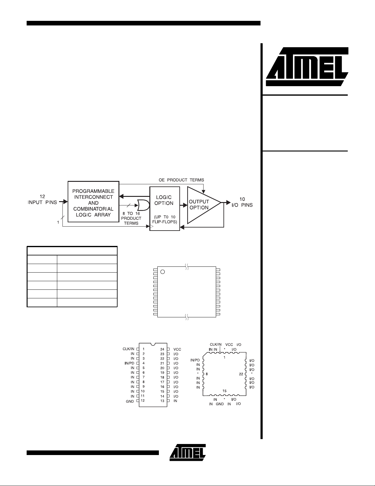
Logic Diagram
Pin Configurations
Pin Name Function
CLK Clock
IN Logic Inputs
I/O Bidirectional Buffers
* No Internal Connection
VCC +5V Supply
PD Power Down
TSSOP Top View
1
CLK/IN
2
IN
3
IN
4
IN/PD
5
IN
6
IN
7
IN
8
IN
9
IN
10
IN
11
IN
12
GND
DIP/SOIC
24
VCC
23
I/O
22
I/O
21
I/O
20
I/O
19
I/O
18
I/O
17
I/O
16
I/O
15
I/O
14
I/O
13
IN
PLCC
ATF22V10C
ATF22V10C
Top view
Note: For PLCC, pins 1, 8, 15 and 22 can be left uncon-
nected. For superior performance, connect V
to pin 1 and ground to 8, 15, 22.
CC
Rev. 0735C/22V10C-D–04/98
Description
The ATF22V10C is a high performance CMOS (Electrically Erasable) Programmable Logic Device (PLD)
which utilizes Atmel’s proven electrically erasable
Flash memory technology. Speeds down to 5 ns and
power dissipation as low as 100 µA are offered. All
speed ran ges are specified ov er the full 5V ± 10%
range for industrial temperature ranges, and 5V ± 5%
for commercial temperature ranges.
Absolute Maximum Ratings*
Several low power options allow selection of the best solution for various types of power-limited applications. Each
of these options significantly reduces total system power
and enhances system reliability.
Temperature Under Bias...................-40°C to +85°C
Storage Temperature......................-65°C to +150°C
Voltage on Any Pin with
Respect to Ground........................-2.0V to +7.0V
(1)
*NOTICE: Stresses beyond those listed under “A bsolute Maxi-
mum Ratings” may cause permanent damage to the device.
This is a stress rating only and functional operation of the
device at these or an y ot he r con ditions beyond those indicated in the oper ational secti ons of this specification is not
implied. Exposure to absolute maximum rating conditions
for extended periods may affect device reliability.
Voltage on Input Pins
with Respect to Ground
During Programming................... -2.0V to +14.0V
Programming Voltage with
Respect to Ground...................... -2.0V to +14.0V
(1)
(1)
Note:
1. Minimum voltage is -0.6V dc, which may undershoot to -2.0V
for pulses of le ss than 20 ns. Maximum output pin volt age is
+ 0.75V dc, which may overshoot to 7. 0V for pulses of
V
CC
less than 20 ns.
DC and AC Operating Conditions
Commercial Industrial
Operating Temperature (Case) 0°C - 70°C -40°C - 85°C
V
Power Supply 5V ± 5% 5V ± 10%
CC
2
ATF22V10C
ATF22V10C
DC Characteristics
Symbol Parameter Condition Min Typ Max Units
I
IL
I
IH
I
CC
I
CC2
I
CC3
I
PD
I
OS
V
IL
V
IH
V
OL
V
OH
Notes: 1. Not more than one output at a time should be shorted.
Input or I/O Low
Leakage Current
Input or I/O High
Leakage Current
Power Supply Current,
Standby
Clocked Power Supply
Current
Clocked Power Supply
Current
Power Supply Current,
PD Mode
Output Short Circuit
(1)
Current
Input Low Voltage -0.5 0.8 V
Input High Voltage 2.0 VCC+0.75 V
Output Low Voltage
Output High Voltage
Duration of short circuit test should not exceed 30 sec.
2. Low frequency only. See Supply Current versus Input Frequency curves.
0 ≤ VIN ≤
V
(MAX)
IL
3.5 ≤ V
V
CC
V
IN
≤ V
IN
= MAX,
= MAX,
Outputs Open
VCC = MAX,
Outputs Open
V
= MAX,
CC
CC
C-5, 7, 10 Com. 85 130 mA
C-10 Ind. 90 140 mA
C-5, 7, 10 Com. 1 mA/MHz
C-10 Ind. 1 mA/MHz
C-5, 7, 10 Com. 150 mA
-35 -10 µA
10 µA
Outputs Open,
f = 15 MHz
V
= MAX Com. 10 100 µA
CC
V
= 0, MAX Ind. 10 100 µA
IN
V
= 0.5V -130 mA
OUT
= VIH or VIL,
V
IN
V
= MIN
CC
= VIH or VIL,
V
IN
V
= MIN
CC
C-10 Ind. 160 mA
= 16 mA Com., Ind. 0.5 V
I
OL
I
= 12 mA Mil. 0.5 V
OL
= -4.0 mA 2.4 V
I
OH
(2)
(2)
3

AC Waveforms
Note: 1. Timing measurement reference is 1.5 V . In pu t AC driv in g le ve ls ar e 0. 0V an d 3.0V, unless otherw is e sp ec ified.
(1)
AC Characteristics
(1)
-5 -7 -10
Symbol Parameter
t
t
PD
CO
Input or Feedback to Combinatorial Output 1 5 3 7.5 3 10 ns
Clock to Output 1 4 2 4.5
Min Max Min Max Min Max Units
(2)
26.5ns
tCF Clock to Feedback 3 3.5 4 ns
tS Input or Feedback Setup Time 3 3.5 4.5 ns
t
H
Hold Time 0 0 0 ns
External Feedback 1/(tS + tCO) 142 125 (3) 90 MHz
F
MAX
Internal Feedback 1/(t
+ tCF) 166 142 117 MHz
S
No Feedback 166 166 125 MHz
t
P
t
W
t
EA
t
ER
t
AP
t
AW
t
AR
t
SP
t
SPR
Notes: 1. See ordering information for valid part numbers.
Clock Period 6 6 8 ns
Clock Width 3 3 3 ns
Input or I/O to Output Enable 2 6 3 7.5 3 10 ns
Input or I/O to Output Disable 2 5 3 7.5 3 9 ns
Input or I/O to Asynchronous Reset of Register 3 7 3 10 3 12 ns
Asynchronous Reset Width 5.5 7 8 ns
Asynchronous Reset Recovery Time 4 5 6 ns
Setup Time, Synchronous Preset 4 4.5 6 ns
Synchronous Preset to Clock Recovery Time 4 5 8 ns
2. 5.5 ns for DIP package devices.
3. 111 MHz for DIP packag e de vi ce s.
4
ATF22V10C

ATF22V10C
Power Down AC Characteristics
Symbol Parameter
t
IVDH
t
GVDH
t
CVDH
t
DHIX
t
DHGX
t
DHCX
t
DLIV
t
DLGV
t
DLCV
t
DLOV
Notes: 1. Output data is la tc hed and held.
Valid Input Before PD High 5 7.5 10 ns
Valid OE Before PD High 0 0 0 ns
Valid Clock Before PD High 0 0 0 ns
Input Don’t Care After PD High 5 7 10 ns
OE Don’t Care After PD High 5 7 10 ns
Clock Don’t Care After PD High 5 7 10 ns
PD Low to Valid Input 5 7.5 10 ns
PD Low to Valid OE 15 20 25 ns
PD Low to Valid Clock 15 20 25 ns
PD Low to Valid Output 20 25 30 ns
2. HI-Z outputs remain HI-Z.
Input Test Waveforms and
Measurement Levels
(1, 2, 3)
-5 -7 -10
Min Max Min Max Min Max
3. Clock and input transitions are ignored.
Output Test Loads:
Commercial
Units
tR, tF < 3 ns
Pin Capacitance
(f = 1 MHz, T = 25°C)
(1)
Typ Max Units Conditions
C
IN
C
OUT
Note: 1. Typical values for nomina l su pply voltage. Thi s param eter is only sampled an d is not 100% tested.
58pFV
68pFV
Power Up Reset
The registers in the ATF22V10Cs are designed to reset
during power up. At a point delayed slight ly from V
crossing V
, all registers will be reset to the low state.
RST
CC
The output state will depend on the polarity of the output
buffer.
This feature is critical for state machine initialization. However, due to the asynchronous nature of reset and the uncertainty of how V
actually rises in the system, the fol-
CC
lowing conditions are required:
1. The V
0.7V,
2. After reset occurs, all input and feedback setup times
must be met before driving the clock pin high, and
3. The clock must remain stable during t
rise must be monotonic, and starts below
CC
= 0V
IN
OUT
= 0V
PR
.
5

POWER
REGISTERED
OUTP UTS
C
LOCK
V
R
ST
t
PR
t
S
t
W
Parameter Description Typ Max Units
t
PR
Power-Up
Reset Time
600 1,000 ns
Power-Up
V
RST
Reset
3.8 4.5 V
Voltage
Preload of Registered Outputs
The ATF22V10C’s registers are provided with circuitry to
allow loading of each register with either a high or a low.
This feature will simplify testing since any st ate can be
forced into the registers to control test sequencing. A
JEDEC file with preload is generated when a source file
with vectors is compiled. Once downloaded, the JE DEC
file preload sequence will be done automatically by most
of the approved programmers after the programming.
Electronic Signature Word
There are 64 bits of programmable memory that are always available to the user, even if the device is secured.
These bits can be used for user-specific data.
Input and I/O Pin Keeper Circuits
The ATF16V8C contains internal input and I/O pin keeper
circuits. These circuits allow each ATF16V 8C pin to hold
its previous value even when it is not being driven by an
external source or by the device’s output buffer. This helps
insure that all logic array inputs are at known, valid logic
levels. This reduces system power by preventing pins
from floating to indeterminate levels. By using pin keeper
Security Fuse Usage
A single fuse is provided to prevent unauthorized copying
of the ATF22V10C fuse patterns. Once programmed, fuse
verify and preload are inhibited. However, the 64-bit User
Signature remains accessible.
The security fuse should be programmed last, as its effect
is immediate.
Programming/Erasing
Programmin g/erasing is performed using standard PLD
programmers. See
Softwar e Support
ming.
circuits rather than pull-up resistors, there is no DC current
required to hold the pins in either logic state (high or low).
These pin keeper circuits are implemented as weak feedback inverters, as shown in the Input Diagram below.
These keeper circuits can easily be overdriven by standard TTL- or CMOS-compatible drivers. The typical overdrive current required is 40 µA.
CMOS PLD Programming Hardware &
for information on software/program-
Input Diagram
6
I/O Diagram
ATF22V10C

Functional Logic Diagram ATF22V10C
ATF22V10C
7

Ordering Information
t
PD
(ns)
5 3 4 ATF22V10C-5JC 28J Commercial
7.5 3.5 4.5 ATF22V10C-7JC 28J Commercial
10 4.5 6.5 ATF22V10C-10JC 28J Commercial
t
S
(ns)
t
CO
(ns)
Ordering Code Package Operation Range
(0°C to 70°C)
ATF22V10C-7PC 24P3 (0°C to 70°C)
ATF22V10C-7SC 24S
ATF22V10C-7XC 24X
ATF22V10C-10PC 24P3 (0°C to 70°C)
ATF22V10C-10SC 24S
ATF22V10C-10XC 24X
ATF22V10C-10JI 28J Industrial
ATF22V10C-10PI 24P3 (-40°C to 85°C)
ATF22V10C-10SI 24S
ATF22V10C-10XI 24X
8
28J
24P3
24S
24X
Package Type
28-Lead, Plastic J-Leaded Chip Carrier (PLCC)
24-Lead, 0.300" Wide, Plastic Dual Inline Package (PDIP)
24-Lead, 0.300" Wid e, Plastic Gull Wing Smal l O ut li ne (SOIC )
24-Lead, 4.4 mm Wide, Plastic Thin Shrink Small Outline (TSSOP)
ATF22V10C
 Loading...