


Effect of RF System Parameters on Receiver
(ATA5745/ATA5746) Sensitivity
1. Introduction
In short-range RF system design, focus is typically placed on transmitter output power
and receiver sensitivity to establish a high-quality RF link. However, due to regulatory
requirements limiting transmitter output power and the plethora of devices that easily
achieve them, often it is the receiver’s sensitivity which remains as the key system
parameter of interest when designing an RF wireless application.
ATA5745
ATA5746
Application Note
Given the choice between two receivers priced the same, what’s the better choice, a
device with a sensitivity of –110 dBm (OOK at 2 Kb/s with a BER of 10
sensitivity of –112 dBm (ASK at 9.6 Kb/s with a BER of 10
to select the device with the best sensitivity number. But, without a theoretical and
empirical understanding of the assumptions used to measure sensitivity, a meaningful
side-by-side comparison of the devices on sensitivity alone becomes nearly
impossible.
A thorough understanding of what receiver sensitivity means, how it is measured, and
how it is affected by other RF system parameters, provides the engineer with a solid
foundation upon which to make design decisions that will result in RF system performance that meets or exceeds the design objection.
The purpose of this document is to explain the concept of RF receiver sensitivity as
well as associated terms such as BER and jitter. These terms will be combined with
other common RF system parameters such as data rate, carrier frequency and modulation format to explore how they interact with and affect the RF receiver performance
of Atmel
®
’s highly integrated UHF ASK/FSK receiver ATA5745.
–3
)? One might be inclined
–2
) or with a
9174A–AUTO–01/10
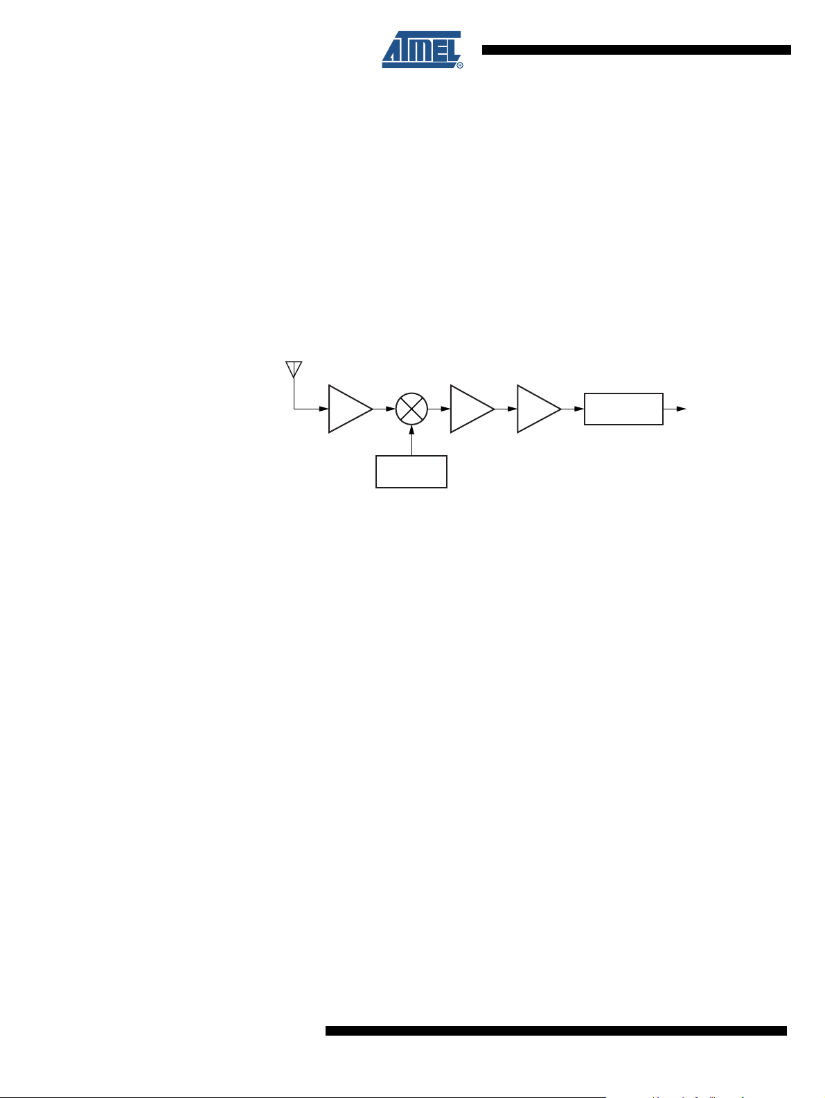
2. Super Heterodyne Receiver
LNA LPF DATA
F
RF
F
LO
FRF - F
LO
IF AMP
Local
Oscillator
Detector
Demodulator
The most common receiver configuration found today in short-range RF wireless applications
is the super heterodyne architecture. The basic principle of operation is the translation of
received RF signals to an intermediate frequency band where the weak input signal is amplified before being applied to a detector. This is achieved by mixing a local oscillator signal FLO
with the received signal FRF to produce an output consisting of FRF + FLO and FRF – FLO. A
lowpass filter typically rejects FRF + FLO and leaves FRF – FLO for further amplification and
filtering. The result is a replica of the modulated RF spectrum that appears translated to a
lower frequency domain called the intermediate frequency (IF). Finally, the detector/demodulator strips off the IF signal and converts what's left into a digital data stream for processing. A
block diagram depicting this general principle is shown in Figure 2-1.
Figure 2-1. Super Heterodyne Receiver Block Diagram
3. Receiver Sensitivity Terminology
In simple terms, receiver sensitivity is defined as the minimum amount of signal power
required at the input of a receiver that results in an accurately demodulated signal “MOST of
the time”. The criterion that defines “MOST of the time” is bit error rate. Input signal power is
expressed in dBm while bit errors are expressed as a rate, usually 10
1000 bits.
There is very little in the way of ambiguity when it comes to measuring signal power applied to
the input of a receiver. RF signal generators are capable of providing accurate output powers
into a standard 50Ω load.
However, when it comes to defining a bit error, there is much more to consider. One can
define a bit error in several different ways. One simple way to measure a bit error rate would
be to count the total actual number of demodulated pulses over a given interval of time and
compare them by the total theoretical number of demodulated pulses over the same interval.
This approach isn’t acceptable because it does not detect changes in pulse width, a phenomenon that may occur as the RF signal grows weaker. For example, Figure 3-1a shows a
theoretical 8-bit modulation stream. Figure 3-1b shows a possible demodulated bit stream at
the output of a receiver. Clearly, the output of the receiver shown in Figure 3-1b would not be
considered acceptable, but according to the bit error criteria defined above, it would not have
any bit errors because both Figure 3-1a and Figure 3-1b possess the same number of pulses
during the defined interval.
-3
or 1 error per every
2
ATA5745/ATA5746
9174A–AUTO–01/10
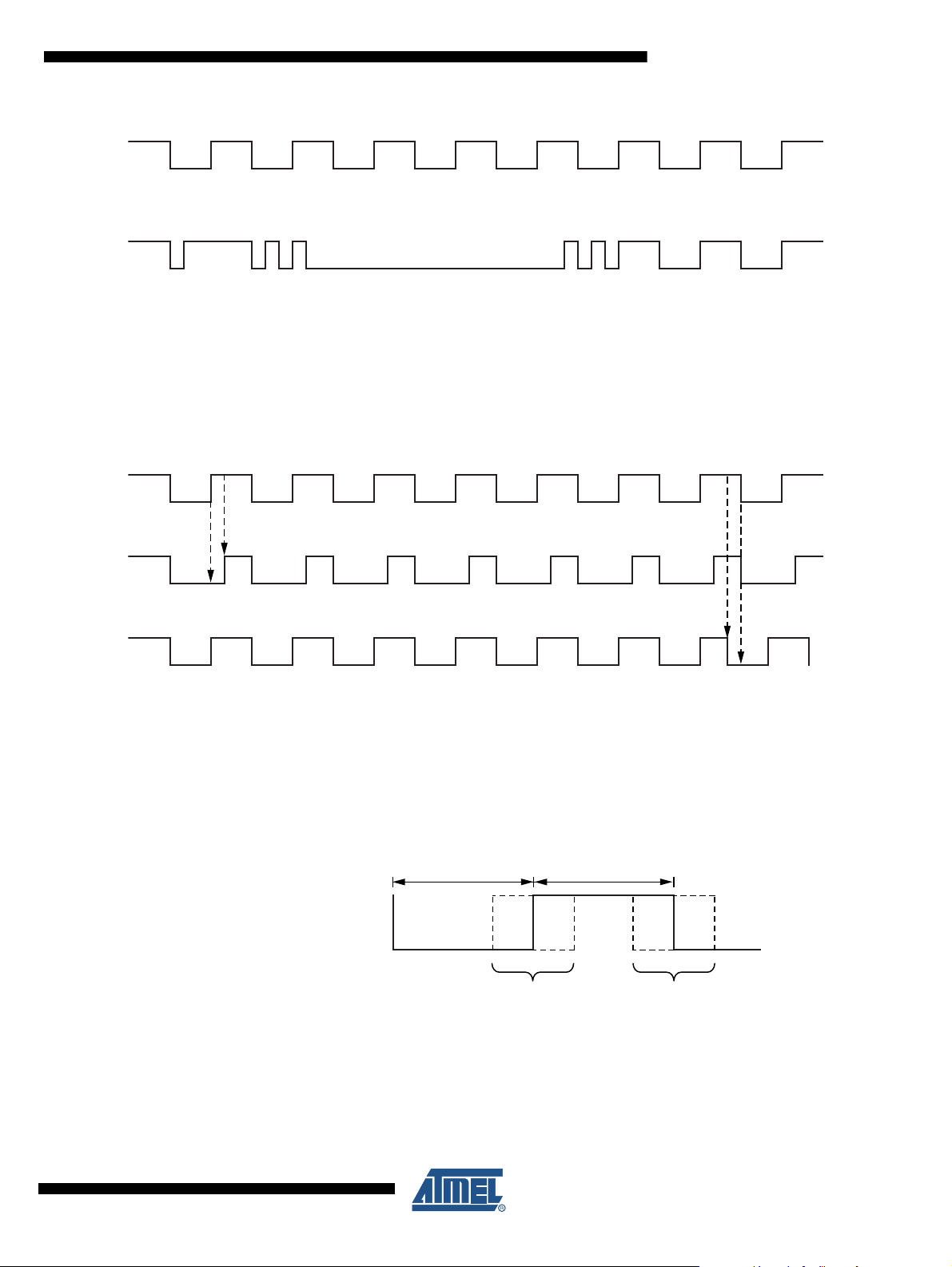
Figure 3-1. Bit Pattern
a
- Reference bit pattern
b - Pulse widt variation jitter, +
Δ
t
1
+Δ t
1
-Δ t
2
c - Phase variation jitter, -Δ t
2
123 45678
123 45678
123 45678
ATA5745/ATA5746
123 45
123 45678
To reconcile this disparity, the concept of “jitter” must be introduced and applied to the bit error
criteria. For the case of demodulated data from an RF receiver, jitter is the unwanted variation
of phase or pulse width in the demodulated signal. Some examples of jitter are shown in Fig-
ure 3-2. Figure 3-2a shows the reference bit pattern and Figure 3-2b and Figure 3-2c show
pulse width and phase jitter, respectively.
Figure 3-2. Examples of Jitter
678
a - Theoretical bit pattern
b - Possible output bit pattern
A common approach for defining a bit error is to create a time limit, ±Δt, that is a percentage of
the edge to edge bit period, T. Using this approach, a bit error would be any bit edge transition
that occurs outside of the time limit window ±Δt. An example of the bit error rate jitter window is
shown in Figure 3-3. In this case, jitter of ±25% is depicted. For the balance of this document,
the default assumption for BER will be 10
-3
with a ±25% jitter window.
Figure 3-3. Reference Signal with Jitter Windows Defining a Bit Error
T
+Δ t
-Δ t
1
Jitter window Jitter window
9174A–AUTO–01/10
T
1
-Δ t2+Δ t
2
3
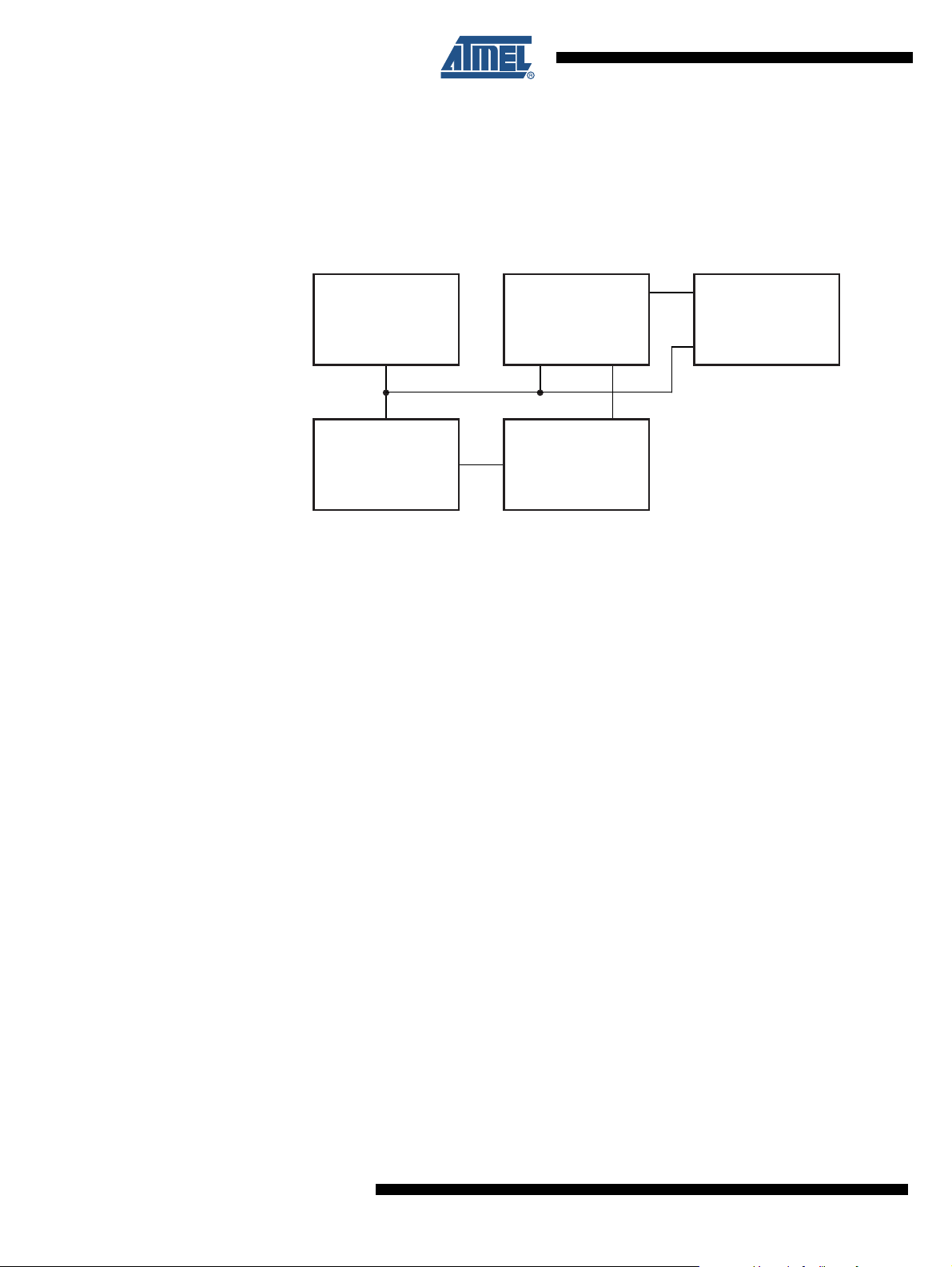
4. Sensitivity Measurements
Several instruments are needed to perform sensitivity measurements; an RF signal generator,
a modulation source, a bit comparator, and a frequency counter. All are common instruments
in a modestly equipped RF lab, with the possible exception of the bit comparator. Please refer
to Figure 4-1 for a configuration drawing showing the interconnection of these instruments.
Figure 4-1. Sensitivity Measurement Set-up
Modulation
Source
F
MOD
Bit
Comparator
F
MOD
F
F
DEMOD
ERROR
Frequency
Counter
F
MOD
RF Signal
Generator
F
RF
RF
IN
DATA
Receiver
Under Test
OUT
The bit comparator used to gather sensitivity data contained in this document is a custom
design and is not commercially available. In simple terms, it generates a pulse, F
ever the demodulated signal, F
respect to the reference signal, F
, exceeds the jitter window (set to ±25% as default) with
DEMOD
. See previous section titled Receiver Sensitivity Termi-
MOD
ERROR
, when-
nology for more details and definitions of jitter and jitter window. The Bit Error Rate is
calculated by dividing the bit comparator’s error signal, F
, by the reference signal, F
ERROR
MOD
Additionally, the bit comparator has provisions to enable the adjustment of the jitter window
from ±10% to ±55%.
The modulation source consisted of a square wave signal whose duty cycle was maintained at
50% and whose frequency was varied. A commonly accepted data bit encoding standard for
low-cost and low data rate RF systems that conforms to this signal definition is Manchester. In
many applications, Manchester yields optimum receiver performance by virtue of the characteristic average DC level of 50% that is present on the demodulated signal.
A pictorial representation of Manchester data bit encoding is supplied in Figure 4-2a and Fig-
ure 4-2b. The bit frame period, T
BIT FRAME
bit “0” appears as a falling edge during T
during T
BIT FRAME
. A key observation to note is that the data bit pattern affects the frequency of
, is defined as the reciprocal of the data rate. A data
BIT FRAME
while a data bit “1” appears as a rising edge
the modulation signal. When alternating data bit polarities are used, e.g., “0101”, the resultant
modulation signal frequency is half the data rate. However, when consecutive “1”s or consecutive “0”s used, the modulation signal frequency is equal to the data rate. In this document, it
was assumed that consecutive data bits of the same polarity were used to generate the modulation signal. This means that a data rate of 1 kB/s will require a modulation source of 1 kHz.
.
4
ATA5745/ATA5746
9174A–AUTO–01/10
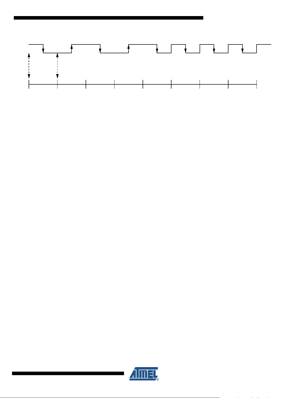
Figure 4-2. Pictorial Representation of Manchester Data Bit Encoding
“0”“1”
T
BIT FRAME
“0”“1”“0”“0”“0”“0”
a - Modulation Signal
b - Data Bit Pattern and Bit Frames
The ATA5746 (315 MHz) reference design was used in this document to gather the typical
data and to show relationships between measured sensitivity as a function of various RF system parameters. Sensitivity data for each graph was obtained from a sample population of ten
boards. The data points shown are based on an average of this population. The trend lines
interpolate behavior between data points and utilize a TBD (e.g., linear, 1st order, log, etc.) to
create best fit. Caution should be exercised before assuming that the results observed on the
Atmel receiver can be extended to receivers from other suppliers without first verifying the
results.
ATA5745/ATA5746
9174A–AUTO–01/10
5
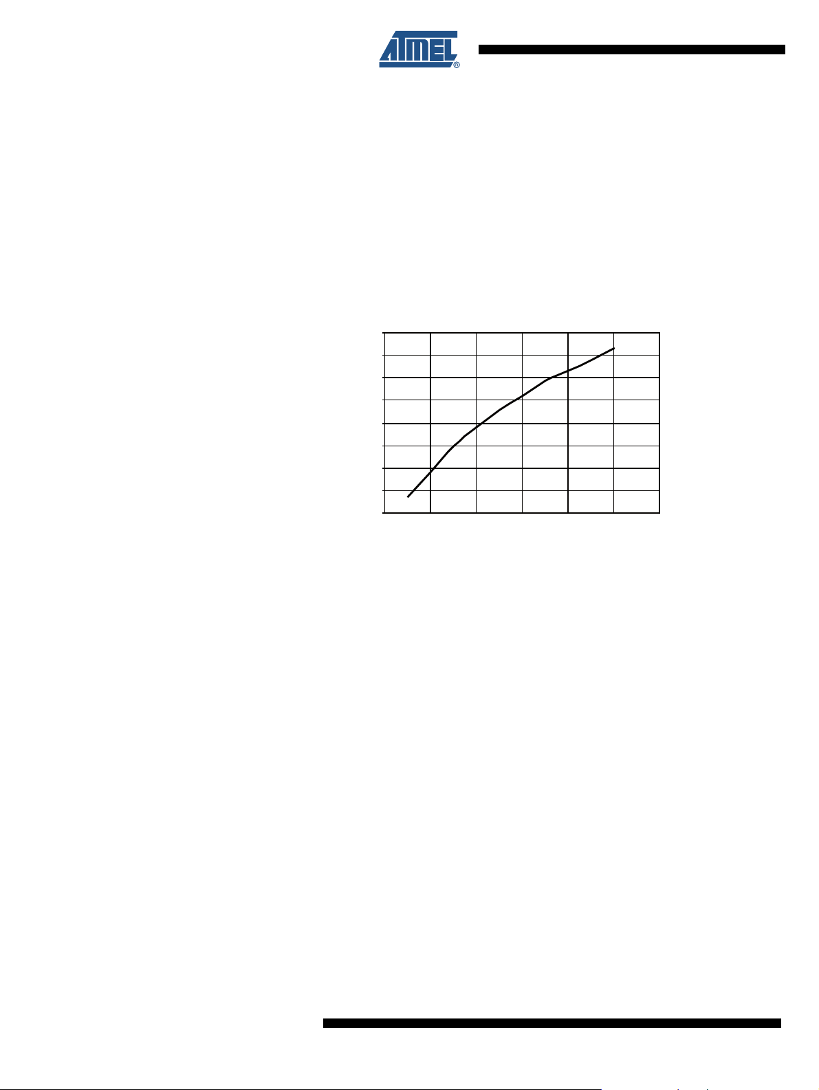
5. Sensitivity as a Function of Data Rate
-116
-115
-114
-113
-112
-111
-110
-109
-108
02468 10 12
Data Rate [kHz]
Sensitivity [dBm]
This section quantifies the effect of data rate on measured sensitivity. Default settings are
Manchester encoding, BER of 10
315 MHz using data rates of 1, 2.5, 5, and 10 Kb/s with ASK modulation.
Receiver sensitivity is a function of the transmission data rate. Consistent with theory, as data
rate goes down, receiver sensitivity goes up. Theoretically, doubling the data rate reduces
sensitivity by 3 dB. Figure 5-1 generally reflects this relationship, especially when comparing
sensitivities at 10 kHz (–108.5 dBm) and 5 kHz (–111.5 dBm).
Figure 5-1. Sensitivity as a Function of Data Rate (ASK)
-3
, and a jitter window of ±25%. Data was measured at
Since the data rate has a substantial effect on the RF receiver’s sensitivity, careful consideration of this system parameter is warranted, especially when designing RF systems for
long-range applications. It is no coincidence that automotive remote start applications commonly use a transmission data rate of less than 1 kHz.
6
ATA5745/ATA5746
9174A–AUTO–01/10

6. Sensitivity as a Function of Modulation
02468 10 12
Data Rate [kHz]
Sensitivity [dBm]
-118
-116
-114
-112
-110
-108
-106
-104
-102
-100
ASK
FSK
OOK
This section quantifies the effect of modulation on measured sensitivity. Default settings are
Manchester encoding, BER of 10
315 MHz using data rates of 1, 2.5, 5, and 10 Kb/s with both ASK and FSK modulation.
Amplitude Shift Keying (ASK) and Frequency Shift Keying (FSK) are two different forms of
modulation that represent digital data as variations in amplitude and frequency changes of a
carrier wave. On-Off Keying (OOK) is a special form of ASK where no carrier is present in a
transmission of a “zero”. By definition, OOK sensitivity is 6 dB lower than ASK sensitivity due
to the lower peak value of transmitted power. Figure 6-1 illustrates the different modulation
types.
Figure 6-1. Modulation Comparison
ATA5745/ATA5746
-3
, and a jitter window of ±25%. Data was measured at
RF devices in the marketplace almost always describe modulation types as either ASK or
FSK. However, ASK as described in Figure 6-1 is rarely implemented. In reality, OOK modulation is most often used when describing an ASK modulation scheme.
Figure 6-2 shows the measured sensitivity using ASK and FSK modulation. OOK sensitivity
was calculated by applying a 6 dB correction from the measured ASK sensitivity. The measurements illustrate that ASK modulated signals yield approximately 7 dB better sensitivity
than FSK modulated signals at similar data rates. However, OOK (the most commonly used
form of ASK), offers very little improvement in sensitivity compared to FSK modulated signals.
Figure 6-2. Sensitivity as a Function of Modulation and Data Rate
9174A–AUTO–01/10
7

7. Sensitivity as a Function of BER
This section quantifies the effect of BER on measured sensitivity. Default settings are Manchester encoding at 1 kB/s, and ±25% jitter. Sensitivity was measured on the same Atmel
receiver using the various bit-error rates commonly used in competitive RF receivers:
-3
10
(Atmel), 2 × 10⁻³(competitor A), 3 × 10⁻³(competitor B), 10-2(competitor C).
Since the following measurements are gathered using a constant 1 kB/s data rate, it may
make more sense to look at bit-error rate as the number of errors allowed per 1000 bit frames.
Table 7-1 shows how each branded receivers' sensitivity parameter relates to the number of
errors allowed per 1000 bit frames.
Table 7-1. Errors Allowed per/1000 Frames
Branded Receiver BER Errors Allowed per 1000 Bit Frames
Atmel 10
Competitor A 2 × 10
Competitor B 3 × 10
Competitor C 10
A higher bit-error rate, or the more errors allowed per 1000 frames, will yield more favorable
sensitivity measurements. As expected, Figure 7-1 shows that measurements conducted
using a BER rate of 10
this in a different way, Atmel receiver sensitivity specified as –115.3 dBm at BER = 10
same as specifying it as –116.6 at BER = 10
-2
gives way to the best sensitivity measurement of –116.6 dBm. Stating
-3
-3
-3
-2
-2
.
10
1
2
3
-3
, is the
Figure 7-1. Sensitivity as a Function of BER (315 MHz; ASK; 1 kHz)
Bit-error Rates
-115.0
-115.2
-115.4
-115.6
-115.8
-116.0
Sensitivity [dBm]
-116.2
-116.4
-116.6
-116.8
-3
10
2 × 10
-3
3 × 10
-3
-2
10
8
ATA5745/ATA5746
9174A–AUTO–01/10

ATA5745/ATA5746
Figure 7-2 shows that this trend is consistent with sensitivity measurements made when the
receiver is modulating a FSK signal.
Figure 7-2. Sensitivity as a Function of BER (315 MHz; FSK; 1 kHz)
Bit-error Rates
-106.5
-107.0
-107.5
-108 .0
-3
10
2 × 10
-3
Sensitivity [dBm]
-108 .5
-109.0
These figures show that the bit-error rate plays a key role in how sensitivity measurements
should be interpreted. For example, a competitive receiver promoted with a sensitivity of
–116 dBm at BER = 10
ity of –115 dBm at BER = 10
-2
would perform worse than an Atmel device with a specified sensitiv-
-3
due to the different BER parameter associated with the
sensitivity. It is important to know that a sensitivity parameter without a BER is meaningless.
When comparing receiver sensitivities, one should always consider the corresponding BER.
3 × 10
-3
-2
10
9174A–AUTO–01/10
9

8. Sensitivity as a Function of Jitter Window
Sensitivity [dBm]
Jitter Window [%]
-116.2
-116.0
-115.8
-115.6
-115.4
-115.2
-115.0
-114.8
-114.6
0 5 10 15 20 25 3 0 3 540 45
This section quantifies the effect of jitter window on measured sensitivity. Default settings are
Manchester encoding at 1 kB/s, and BER of 10
433.92 MHz using jitter windows of ±10%, ±25%, ±40% for ASK modulation. The jitter window
is used to address changes in pulse width as the received RF signal grows weaker. Generally,
a ±25% jitter window is used for sensitivity measurements. In this section the relationship
between measured sensitivity and jitter window size will be analyzed.
As the jitter windows increases, the evaluation window decreases. For example, a ±25% jitter
window will yield a 50% evaluation window, and increasing the jitter window to ±40% will result
in a 20% evaluation window. Figure 8-1 illustrates this relationship.
Figure 8-1. Reference Signal with Jitter Windows and Evaluation Window
-Δ t
Evaluation window
+Δ t
1
1
-3
. Data will be measured at 315 MHz and
-Δ t2+Δ t
2
As the received RF signal grows weaker, changes in pulse widths become greater and more
inconsistent. As the jitter window size increases, the evaluation window is narrowed and
becomes less susceptible to this phenomenon. Figure 8-2 shows that received sensitivity
improves as the jitter window is increased.
Figure 8-2. Sensitivity as a Function of Jitter Window Size
Knowing that a wider jitter window will result in better receiver sensitivity has implications on
the design of the baseband software. It is important to note that poorly designed baseband
decoding can significantly degrade RF system performance.
Jitter window
Jitter window
10
ATA5745/ATA5746
9174A–AUTO–01/10

ATA5745/ATA5746
To address this, an idea worth considering would be the application of a delay after a bit transition detection. This principal is illustrated in Figure 8-3.
Figure 8-3. Decode Routine Using Delay Function
Detect Bit Transistion
Evaluation window
Add Delay
Function
+Δ t
-Δ t
1
1
-Δ t2+Δ t
2
Jitter window
Jitter window
Evaluate state
9174A–AUTO–01/10
11

9. Sensitivity as a Function of Frequency Deviation (FSK)
314.962 MHz
315 MHz 315.038 MHz
-38 kHz +38 kHz
Sensitivity [dBm]
Frequency Deviation [kHz]
-108
-107
-106
-105
-104
-103
-102
-101
02040608 0100120140
This section quantifies the effect of frequency deviation on sensitivity. Default setting is
±38 kHz as stated in the datasheet. Sensitivity was measured using frequency deviations
swept from ±15 kHz to ±120 kHz for FSK modulation.
Frequency deviation is the distance between the two frequencies as show in Figure 9-1.
Figure 9-1. Frequency Deviation
The ATA5746 datasheet states that the demodulator is optimized to receive a FSK signal with
frequency deviations from ±18 kHz to ±50 kHz with a default setting of ±38 kHz. Figure 9-2
illustrates that performance starts to fall off at frequency deviations above and below this optimal setting.
Figure 9-2. Sensitivity as a Function of Frequency Deviation
12
ATA5745/ATA5746
9174A–AUTO–01/10

9.1 Conclusion
ATA5745/ATA5746
Sensitivity measurements show that data rate has the largest effect on sensitivity. Data rates
ranging from 1 kHz to 10 kHz yielded differences in sensitivity up to 7 dB. The next most significant parameter is jitter window size. As the jitter windows size increases, the evaluation
window narrows and the receiver's performance improves drastically. The frequency deviation
in an FSK-modulated signal is an important parameter to consider when developing an RF
system. In this case, the ATA5746 receiver recommends a ±38 kHz deviation. Testing shows
that signals with frequency deviations straying from the recommended value negatively
impacts the receiver’s performance. Sensitivity as a function of BER is important to consider
given that manufacturers use different bit error rates when specifying a receiver's sensitivity. It
is important to compare “apples to apples” when selecting a receiver. Unless the sensitivity figure of receivers under consideration is compared using the same BER criteria, the resulting
decision will be flawed. Finally, comparisons in modulations schemes shows that ASK-modulated signals yield much better sensitivity than FSK-modulated signals. However, these results
don’t hold too much currency considering “true” ASK is rarely used in the real world. In reality,
OOK is most often used when describing an ASK RF system. Measurements showed that
OOK-modulated signals yielded very similar sensitivity results when compared to FSK-modulated signals.
RF receiver sensitivity is affected by a number of system parameters. It is important to recognize that sensitivity measurements need to be evaluated with the knowledge of the entire RF
system. Data rate, modulation schemes, BER, jitter window, and frequency deviation all contribute to a receiver’s performance.
The ATA5746 receiver was used for all measurements discussed in this application note.
However, the same principles apply to all receivers including Atmel's entire of line of receivers
shown in Table 9-1.
Table 9-1. Atmel Receivers
Atmel Receivers Market Frequency
ATA5745 Automotive 433 MHz
ATA5746 Automotive 315 MHz
ATA5723 Automotive 315 MHz
ATA5724 Automotive 433 MHz
ATA5728 Automotive 868 MHz
ATA8201 Industrial 315 MHz
ATA8202 Industrial 433 MHz
ATA8203 Industrial 315 MHz
ATA8204 Industrial 433 MHz
ATA8205 Industrial 868 MHz
For more information on Atmel’s RF automotive devices visit:
http://www.atmel.com/products/caraccess/default.asp
For more information on Atmel’s industrial RF devices visit:
http://www.atmel.com/products/smartRF/default.asp
9174A–AUTO–01/10
13

Headquarters International
Atmel Corporation
2325 Orchard Parkway
San Jose, CA 95131
USA
Tel: 1(408) 441-0311
Fax: 1(408) 487-2600
Atmel Asia
Unit 1-5 & 16, 19/F
BEA Tower, Millennium City 5
418 Kwun Tong Road
Kwun Tong, Kowloon
Hong Kong
Tel: (852) 2245-6100
Fax: (852) 2722-1369
Product Contact
Web Site
www.atmel.com
Literature Requests
www.atmel.com/literature
Atmel Europe
Le Krebs
8, Rue Jean-Pierre Timbaud
BP 309
78054
Saint-Quentin-en-Yvelines Cedex
France
Tel: (33) 1-30-60-70-00
Fax: (33) 1-30-60-71-11
Technical Support
car_access@atmel.com
Atmel Japan
9F, Tonetsu Shinkawa Bldg.
1-24-8 Shinkawa
Chuo-ku, Tokyo 104-0033
Japan
Tel: (81) 3-3523-3551
Fax: (81) 3-3523-7581
Sales Contact
www.atmel.com/contacts
Disclaimer: The information in this document is provided in connection with Atmel products. No license, express or implied, by estoppel or otherwise, to any
intellectual property right is granted by this document or in connection with the sale of Atmel products. EXCEPT AS SET FORTH IN ATMEL’S TERMS AND CONDI-
TIONS OF SALE LOCATED ON ATMEL’S WEB SITE, ATMEL ASSUMES NO LIABILITY WHATSOEVER AND DISCLAIMS ANY EXPRESS, IMPLIED OR STATUTORY
WARRANTY RELATING TO ITS PRODUCTS INCLUDING, BUT NOT LIMITED TO, THE IMPLIED WARRANTY OF MERCHANTABILITY, FITNESS FOR A PARTICULAR
PURPOSE, OR NON-INFRINGEMENT. IN NO EVENT SHALL ATMEL BE LIABLE FOR ANY DIRECT, INDIRECT, CONSEQUENTIAL, PUNITIVE, SPECIAL OR INCIDENTAL DAMAGES (INCLUDING, WITHOUT LIMITATION, DAMAGES FOR LOSS OF PROFITS, BUSINESS INTERRUPTION, OR LOSS OF INFORMATION) ARISING OUT OF
THE USE OR INABILITY TO USE THIS DOCUMENT, EVEN IF ATMEL HAS BEEN ADVISED OF THE POSSIBILITY OF SUCH DAMAGES. Atmel makes no
representations or warranties with respect to the accuracy or completeness of the contents of this document and reserves the right to make changes to specifications
and product descriptions at any time without notice. Atmel does not make any commitment to update the information contained herein. Unless specifically provided
otherwise, Atmel products are not suitable for, and shall not be used in, automotive applications. Atmel’s products are not intended, authorized, or warranted for use
as components in applications intended to support or sustain life.
© 2010 Atmel Corporation. All rights reserved. Atmel®, logo and combinations thereof, and others are registered trademarks or trademarks of
Atmel Corporation or its subsidiaries. Other terms and product names may be trademarks of others.
9174A–AUTO–01/10
 Loading...