

Page 1
1
2
3
4
8
7
6
5
CS
SK
DI
DO
VCC
DC
NC
GND
1
2
3
4
8
7
6
5
CS
SK
DI
DO
VCC
DC
NC
GND
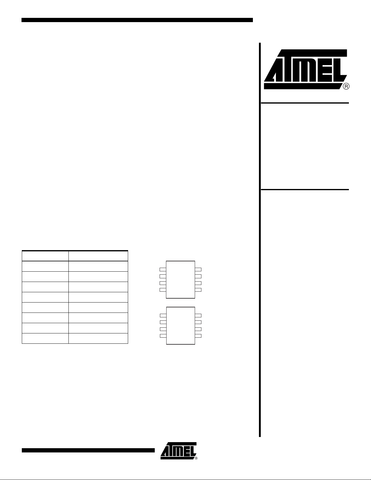
8-lead SOIC
8-lead TSSOP
BDTIC www.bdtic.com/ATMEL
Features
• Low-voltage and Standard-voltage Operation
– 2.7 (VCC = 2.7V to 5.5V)
• Three-wire Serial Interface
• 2 MHz Clock Rate Compatibility
• Self-timed Write Cycle (10 ms max)
• High Reliability
– Endurance: 1 Million Write Cycles
– Data Retention: 100 Years
• Lead-free/Halogen-free Devices Available
• 8-lead JEDEC SOIC and 8-lead TSSOP Packages
Three-wire
Description
The AT93C46A provides 1024 bits of serial electrically-erasable programmable readonly memory (EEPROM) organized as 64 words of 16 bits each. The device is optimized for use in many automotive applications where low-power and low-voltage
operation
SOIC and 8-lead TSSOP packages.
The AT93C46A is enabled through the Chip Select pin (CS) and accessed via a threewire s
(SK). Upon receiving a Read instruction at DI, the address is decoded and the data is
clocked out serially on the data output pin DO. The write cycle is completely self-timed
and no separate erase cycle is required before write. The write cycle is only enabled
when the part is in the erase/write enable state. When CS is brought high following the
initiation of a write cycle, the DO pin outputs the ready/busy status of the part.
The AT93C46A is available in 2.7V to 5.5V versions.
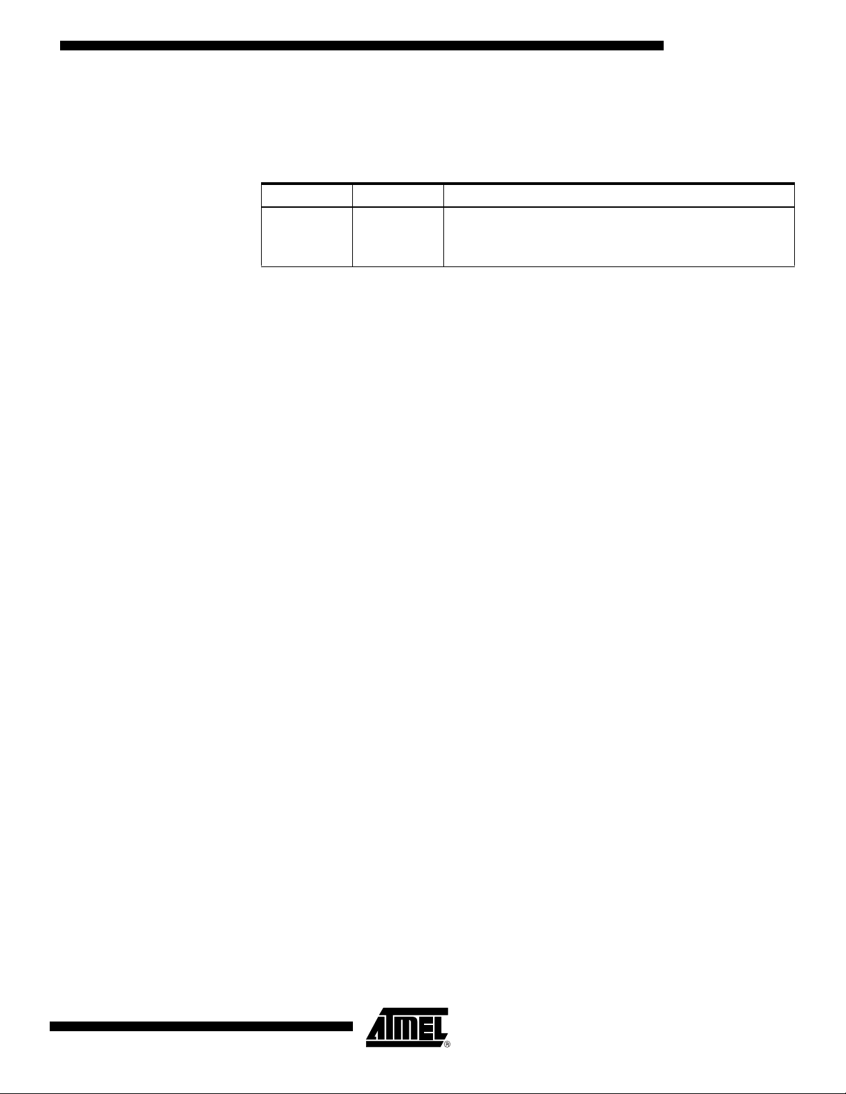
Table 1. Pin Configuration
Pin Name Function
CS Chip Select
SK Serial Data Clock
DI Serial Data Input
DO Serial Data Output
GND Ground
VCC Power Supply
NC No Connect
are essential. The AT93C46A is available in space-saving 8-lead JEDEC
erial interface consisting of Data Input (DI), Data Output (DO), and Shift Clock
Automotive
Temperature
Serial EEPROM
1K (64 x 16)
AT93C46A
DC Don’t Connect
5089B–SEEPR–2/07
Page 2
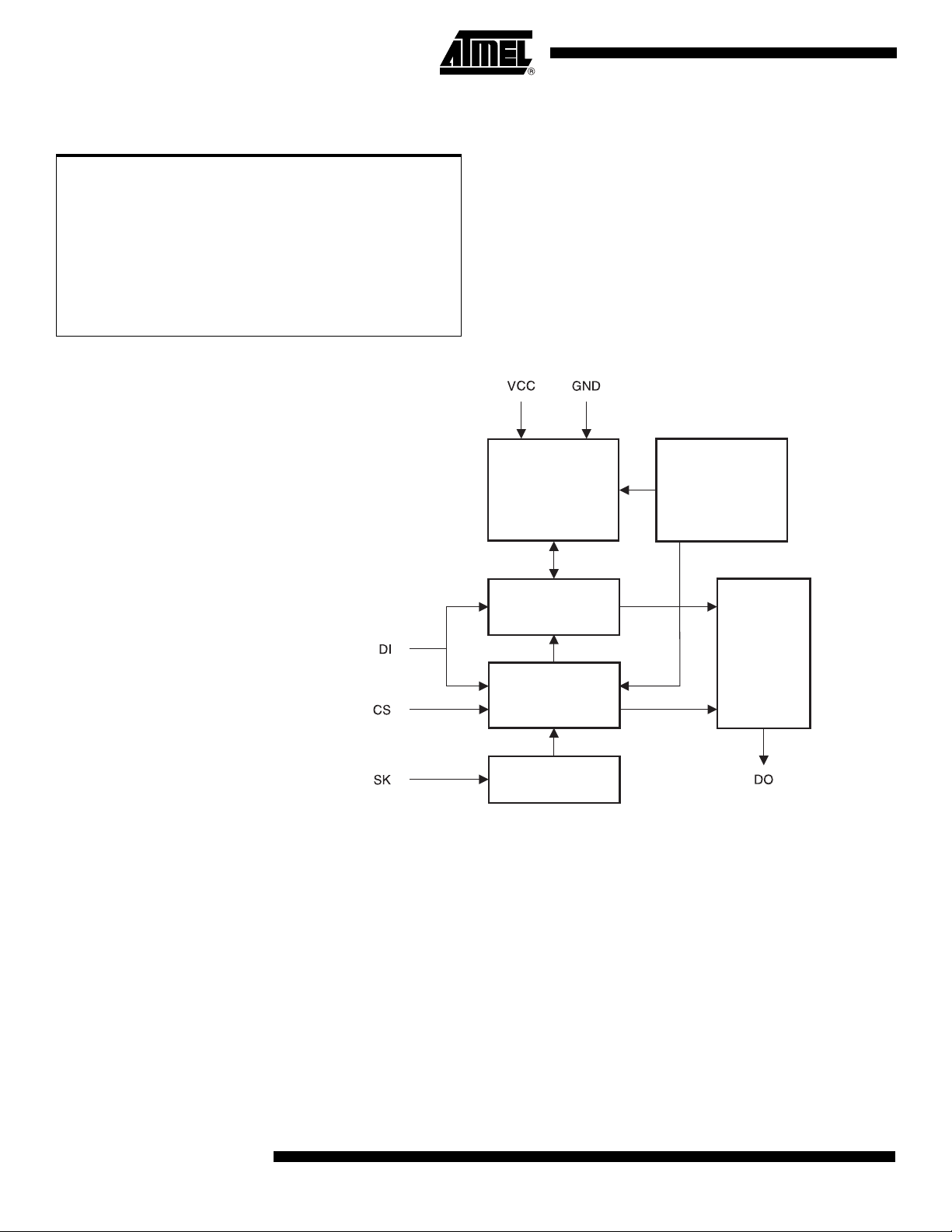
Absolute Maximum Ratings*
MEMORY ARRAY
64 x 16
ADDRESS
DECODER
OUTPUT
BUFFER
DATA
REGISTER
MODE
DECODE
LOGIC
CLOCK
GENERATOR
Operating Temperature......................................−55°C to +125°C
Storage Temperature .
Voltage on Any Pin
with Respect to Ground ........................................ −1.0V to +7.0V
Maximum Operating Voltage .......................................... 6.25V
DC Output Current........................................................ 5.0 mA
........................................−65°C to +150°C
Figure 1. Block Diagram
*NOTICE: Stresses beyond those listed under “Absolute
Maximum Ratings” may cause permanent damage to the device. This is a stress rating only and
nctional operation of the device at these or any
fu
other conditions beyond those indicated in the
operational sections of this specification is not
implied. Exposure to absolute maximum rating
conditions for extended periods may affect
device reliability.
2
AT93C46A
5089B–SEEPR–2/07
Page 3
AT93C46A
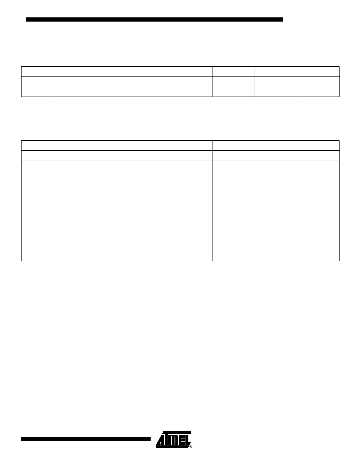
Table 2. Pin Capacitance
Applicable over recommended operating range from TA = 25°C, f = 1.0 MHz, VCC = +5.0V (unless otherwise noted)
Symbol Test Conditions Max Units Conditions
C
OUT
C
IN
Output Capacitance (DO) 5 pF V
Input Capacitance (CS, SK, DI) 5 pF VIN = 0V
Note: This parameter is characterized and is not 100% tested.
Table 3. DC Characteristics
OUT
= 0V
Applicable over recommended operating range from: T
= −40°C to +125°C, VCC = +2.7V to +5.5V,
A
(unless otherwise noted).
Symbol Parameter Test Condition Min Typ Max Unit
V
CC1
I
CC
I
SB1
I
SB2
I
IL
I
OL
(1)
V
IL1
(1)
V
IH1
V
OL1
V
OH1
Note: 1. VIL min and VIH max are reference only and are not tested.
Supply Voltage 2.7 5.5 V
Read at 1.0 MHz 0.5 2.0 mA
Supply Current VCC = 5.0V
Write at 1.0 MHz 0.5 2.0 mA
Standby Current VCC = 2.7V CS = 0V 6.0 10.0 µA
Standby Current VCC = 5.0V CS = 0V 10.0 15.0 µA
Input Leakage VIN = 0V to VCC 0.1 3.0 µA
Output Leakage VIN = 0V to VCC 0.1 3.0 µA
Input Low Voltage 2.7V ≤ VCC ≤ 5.5V −0.6 0.8 V
Input High Voltage 2.7V ≤ VCC ≤ 5.5V 2.0 VCC + 1 V
Output Low Voltage 2.7V ≤ VCC ≤ 5.5V IOL = 2.1 mA 0.4 V
Output High Voltage 2.7V ≤ VCC ≤ 5.5V IOH = −0.4 mA 2.4
5089B–SEEPR–2/07
3
Page 4
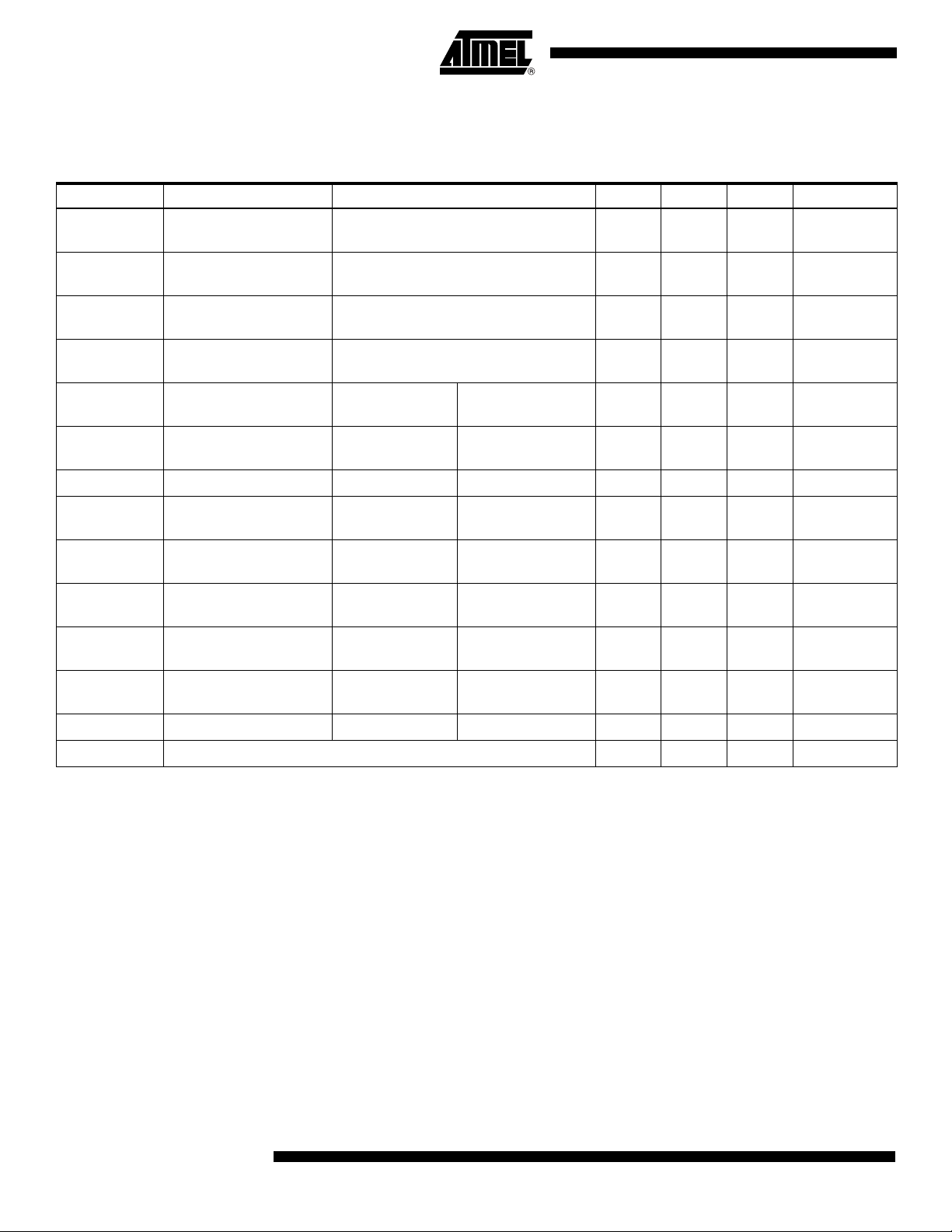
Table 4. AC Characteristics
Applicable over recommended operating range from T
= −40°C to + 125°C, VCC = As Specified, CL = 1 TTL Gate and
A
100 pF (unless otherwise noted)
Symbol Parameter Test Condition Min Typ Max Units
f
SK
t
SKH
t
SKL
t
CS
t
CSS
t
DIS
t
CSH
t
DIH
t
PD1
t
PD0
SK Clock Frequency
SK High Time
SK Low Time
Minimum CS Low Time
4.5V ≤ V
2.7V ≤ V
4.5V ≤ V
2.7V ≤ VCC ≤ 5.5V
4.5V ≤ V
2.7V ≤ VCC ≤ 5.5V
4.5V ≤ V
2.7V ≤ V
≤ 5.5V
CC
≤ 5.5V
CC
≤ 5.5V
CC
≤ 5.5V
CC
≤ 5.5V
CC
≤ 5.5V
CC
CS Setup Time Relative to SK
DI Setup Time Relative to SK
4.5V ≤ V
≤ 5.5V
CC
2.7V ≤ VCC ≤ 5.5V
4.5V ≤ V
≤ 5.5V
CC
2.7V ≤ VCC ≤ 5.5V
0
0
250
250
250
250
250
25
50
50
100
100
0
CS Hold Time Relative to SK 0 ns
DI Hold Time Relative to SK
Output Delay to “1” AC Test
Output Delay to “0” AC Test
4.5V ≤ V
2.7V ≤ VCC ≤ 5.5V
4.5V ≤ V
2.7V ≤ V
4.5V ≤ V
2.7V ≤ VCC ≤ 5.5V
≤ 5.5V
CC
≤ 5.5V
CC
≤ 5.5V
CC
≤ 5.5V
CC
100
100
2
1
250
500
250
500
MHz
ns
ns
ns
ns
ns
ns
ns
ns
t
SV
t
DF
t
WP
Endurance
CS to Status Valid AC Test
CS to DO in High
Impedance
AC Test
CS = V
IL
Write Cycle Time 2.7V ≤ VCC ≤ 5.5V 0.1 3 10 ms
(1)
5.0V, 25°C 1M Write Cycles
4.5V ≤ V
2.7V ≤ VCC ≤ 5.5V
4.5V ≤ VCC ≤ 5.5V
2.7V ≤ V
Note: 1. This parameter is characterized and is not 100% tested.
≤ 5.5V
CC
≤ 5.5V
CC
250
250
100
150
ns
ns
4
AT93C46A
5089B–SEEPR–2/07
Page 5

AT93C46A
Functional Description
The AT93C46A is accessed via a simple and versatile three-wire serial communication
interface. Device operation is controlled by seven instructions issued by the host processor. A valid instruction starts with a rising edge of CS and consists of a start bit (logic
“1”) followed by the appropriate op code and the desired memory address location.
Table 5. Instruction Set for the AT93C46A
Address
Instruction SB Op Code
READ 1 10 A
EWEN 1 00 11XXXX Write enable must precede all programming modes.
ERASE 1 11 A
WRITE 1 01 A
ERAL 1 00 10XXXX Erases all memory locations. Valid only at V
WRAL 1 00 01XXXX Writes all memory locations. Valid only at V
EWDS 1 00 00XXXX Disables all programming instructions.
− A
5
5
− A
5
− A
0
0
0
Commentsx 16
Reads data stored in memory, at specified address.
Erase memory location An − A0.
Writes memory location An − A0.
READ (READ): The Read (READ) instruction contains the address code for the memory location to be read. After the instruction and address are decoded, data from the
selected memory location is available at the serial output pin DO. Output data changes
are synchronized with the rising edges of serial clock SK. It should be noted that a
dummy bit (logic “0”) precedes the 16-bit data output string.
= 4.5V to 5.5V.
CC
= 4.5V to 5.5V.
CC
ERASE/WRITE ENABLE (EWEN): To assure data integrity, the part automatically goes
into the Erase/Write Disable (EWDS) state when power is first applied. An Erase/Write
Enable (EWEN) instruction must be executed first before any programming instructions
can be carried out. Please note that once in the EWEN state, programming remains
enabled until an EWDS instruction is executed or V
power is removed from the part.
CC
ERASE (ERASE): The Erase (ERASE) instruction programs all bits in the specified
memory location to the logical “1” state. The self-timed erase cycle starts once the
Erase instruction and address are decoded. The DO pin outputs the ready/busy status
of the part if CS is brought high after being kept low for a minimum of 250 ns (t
CS
). A
logic “1” at pin DO indicates that the selected memory location has been erased and the
part is ready for another instruction.
WRITE (WRITE): The Write (WRITE) instruction contains the 16 bits of data to be written into the specified memory location. The self-timed programming cycle, t
, starts
WP
after the last bit of data is received at serial data input pin DI. The DO pin outputs the
ready/busy status of the part if CS is brought high after being kept low for a minimum of
250 ns (t
). A logic “0” at DO indicates that programming is still in progress. A logic “1”
CS
indicates that the memory location at the specified address has been written with the
data pattern contained in the instruction and the part is ready for further instructions. A
ready/busy status cannot be obtained if the CS is brought high after the end of the selftimed programming cycle, t
WP
.
ERASE ALL (ERAL): The Erase All (ERAL) instruction programs every bit in the memory array to the logic “1” state and is primarily used for testing purposes. The DO pin
outputs the READY/BUSY status of the part if CS is brought high after being kept low for
a minimum of 250 ns (t
). The ERAL instruction is valid only at VCC = 5.0V ± 10%.
CS
WRITE ALL (WRAL): The Write All (WRAL) instruction programs all memory locations
with the data patterns specified in the instruction. The DO pin outputs the READY/BUSY
5089B–SEEPR–2/07
5
Page 6

status of the part if CS is brought high after being kept low for a minimum of 250 ns (tCS).
The WRAL instruction is valid only at V
ERASE/WRITE DISABLE (EWDS): To protect against accidental data disturb, the
Erase/Write Disable (EWDS) instruction disables all programming modes and should be
executed after all programming operations. The operation of the READ instruction is
independent of both the EWEN and EWDS instructions and can be executed at any
time.
Timing Diagrams
Figure 2. Synchronous Data Timing
= 5.0V ± 10%.
CC
μ
Note: 1. This is the minimum SK period.
Table 6 . Organization Key for Timing Diagrams
I/O
A
D
AT93C46A
x 16
N
N
A
5
D
15
6
AT93C46A
5089B–SEEPR–2/07
Page 7

Figure 3. READ Timing
High Impedance
t
CS
CS
t
CS
SK
DI 1 0
000
...
Figure 4. EWEN Timing
CS
(1)
AT93C46A
t
CS
SK
DI
Note: 1. Requires a minimum of nine clock cycles.
Figure 5. EWDS Timing
Note: 1. Requires a minimum of nine clock cycles.
(1)
001
11
...
5089B–SEEPR–2/07
7
Page 8
Figure 6. WRITE Timing
SK
CS
t
CS
t
WP
11
A
N
D
N
0A0D0
... ...
DI
DO
HIGH IMPEDANCE
BUSY
READY
Figure 7. WRAL Timing
(1,2)
CS
SK
DI
DO
Notes: 1. Valid only at VCC = 4.5V to 5.5V.
2. Requires a minimum of nine clock cycles.
HIGH IMPEDANCE
1 0 0 1 ... D
t
CS
... D00
N
BUSY
READY
t
WP
8
AT93C46A
5089B–SEEPR–2/07
Page 9
Figure 8. ERASE Timing
SK
1 1 ...1
CS
DI A
N
t
CS
t
SV
t
DF
t
WP
A
N-1AN-2
A0
CHECK
STATUS
STANDBY
READY
BUSY
DO
HIGH IMPEDANCE
HIGH IMPEDANCE
SK
CS
DI 1 1000
DO
HIGH IMPEDANCE
HIGH IMPEDANCE
READY
BUSY
CHECK
STATUS
STANDBY
t
WP
t
CS
t
SV
t
DF
Figure 9. ERAL Timing
(1)
AT93C46A
Note: 1. Valid only at VCC = 4.5V to 5.5V.
5089B–SEEPR–2/07
9
Page 10
Ordering Information
Ordering Code Package Operation Range
AT93C46A-10SQ-2.7
AT93C46A-10TQ-2.7
8S1
8A2
Lead-free/Halogen-free/
ded Temperature
Exten
(−40°C to
125°C)
Package Type
8S1 8-lead, 0.150" Wide, Plastic Gull Wing Small Outline (JEDEC SOIC)
8A2 8-lead, 0.170" Wide, Thin Shrink Small Outline Package (TSSOP)
Options
−2.7 Low Voltage (2.7V to 5.5V)
10
AT93C46A
5089B–SEEPR–2/07
Page 11

Packaging Information
1150 E. Cheyenne Mtn. Blvd.
Colorado Springs, CO 80906
TITLE
DRAWING NO.
R
REV.
Note:
10/7/03
8S1, 8-lead (0.150" Wide Body), Plastic Gull Wing
Small Outline (JEDEC SOIC)
8S1 B
COMMON DIMENSIONS
(Unit of Measure = mm)
SYMBOL
MIN
NOM
MAX
NOTE
A1 0.10 – 0.25
These drawings are for general information only. Refer to JEDEC Drawing MS-012, Variation AA for proper dimensions, tolerances, datums, etc.
A 1.35 – 1.75
b 0.31 – 0.51
C 0.17 – 0.25
D 4.80 – 5.00
E1 3.81 – 3.99
E 5.79 – 6.20
e 1.27 BSC
L 0.40 – 1.27
∅ 0˚ – 8˚
∅
Top View
End View
Side View
e
B
D
A
A1
N
E
1
C
E1
L
8S1 – JEDEC SOIC
AT93C46A
5089B–SEEPR–2/07
11
Page 12
8A2 –TSSOP
2325 Orchard Parkway
San Jose, CA 95131
TITLE
DRAWING NO.
R
REV.
5/30/02
COMMON DIMENSIONS
(Unit of Measure = mm)
SYMBOL
MIN
NOM
MAX
NOTE
D 2.90 3.00 3.10 2, 5
E 6.40 BSC
E1 4.30 4.40 4.50 3, 5
A – – 1.20
A2 0.80 1.00 1.05
b 0.19 – 0.30 4
e 0.65 BSC
L 0.45 0.60 0.75
L1 1.00 REF
8A2, 8-lead, 4.4 mm Body, Plastic
Thin Shrink Small Outline Package (TSSOP)
Notes: 1. This drawing is for general information only. Refer to JEDEC Drawing MO-153, Variation AA, for proper dimensions, tolerances,
datums, etc.
2. Dimension D does not include mold Flash, protrusions or gate burrs. Mold Flash, protrusions and gate burrs shall not exceed
0.15 mm (0.006 in) per side.
3. Dimension E1 does not include inter-lead Flash or protrusions. Inter-lead Flash and protrusions shall not exceed 0.25 mm
(0.010 in) per side.
4. Dimension b does not include Dambar protrusion. Allowable Dambar protrusion shall be 0.08 mm total in excess of the
b dimension at maximum material condition. Dambar cannot be located on the lower radius of the foot. Minimum space between
protrusion and adjacent lead is 0.07 mm.
5. Dimension D and E1 to be determined at Datum Plane H.
8A2
B
Side View
End View
Top View
A2
A
L
L1
D
123
E1
N
b
Pin 1 indicator
this corner
E
e
12
AT93C46A
5089B–SEEPR–2/07
Page 13
Revision History
AT93C46A
Doc. Rev. Date Comments
5089B 1/2007 Implemented revision history
Removed PDIP package offering
Removed Pb’d parts
5089B–SEEPR–2/07
13
 Loading...