


Features
®
•
•
•
•
•
•
•
•
•
•
•
•
•
•
•
•
•
AVR
- High Performance and Low Power RISC Architecture
89 Powerful Instructions - Most Single Clock Cycle Execution
1K bytes of In-System Reprogrammable Flash
– SPI Serial Interface for Program Downloading
– Endurance: 1,000 Write/Eras e Cycles
64 bytes EEPROM
– Endurance: 100,000 Write/Erase Cycles
32 x 8 General Purpose Working Registers
15 Programmable I/O Lines
VCC: 2.7 - 6.0V
Fully Static Operation
– 0 - 12 MHz, 4.0 - 6.0V
– 0 - 4 MHz, 2.7 - 6.0V
Up to 12 MIPS Throughput at 12 MHz
One 8-Bit Timer/Counter with Separate Prescaler
External and Internal Interrupt Sources
Programmable Watchdog Timer with On-Chip Oscillator
On-Chip Analog Comparator
Low Power Idle and Power Down Modes
Programming Lock for Software Security
20-Pin Device
Selectable On-Chip RC Oscillator for Zero External Components
Description
The AT90S1200 is a low-power CMOS 8-bit microcontroller based on the
enhanced RISC architecture . By exe cuting powe rful instruc tions in a single clock
cycle, the AT90S1200 achieves throughpu ts approaching 1 MIPS per MHz allowing
the system designer to optimize power consumption versus processing speed.
The AVR core combin es a rich instruc tion set with th e 32 general pur pose workin g
registers. All the 32 registers are directly connected to the Arithmetic Logic Unit (ALU),
allowing two indep endent r egisters to be acce ssed in one single instruc tion exe cuted
in one clock cycle. Th e resulting arc hitecture is mor e code efficie nt while achievin g
throughputs up to ten times faster than conventional CISC microcontrollers.
AVR
(continued)
8-Bit
Microcontr oller
with 1K bytes
In-System
Programmable
Flash
AT90S1200
Pin Configuration
Rev. 0838DS–07/98
Note: This is a summary document. For the complete 48 page
datasheet, please visit our web site at
literature@atmel.com
mail at
and request literature #0838D.
www.atmel.com
or e-
1
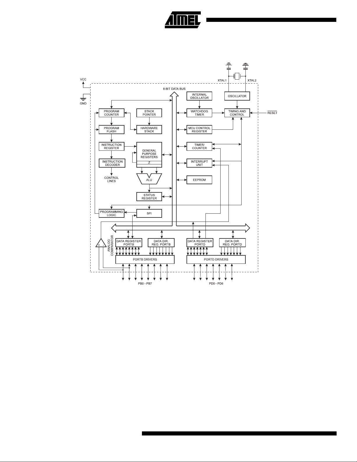
Block Diagram
Figure 1.
The AT90S1200 Block Diagram
The architectu re suppor ts high level languages efficient ly
as well as extremely dense assembler code programs. The
AT90S1200 provides the following features: 1K bytes of InSystem Progra mmabl e Flash , 64 bytes EEPRO M, 15 ge neral purpose I/O lines, 32 general purpo se working re gisters, internal and external interrupts, programmable
Watchdog Timer with internal oscillator, an SPI serial port
for program downloading and two software selectabl e
power saving modes. The Idle Mode stops the CPU while
allowing the registers, timer/counter, watchdog and interrupt system to continue functioning. The power down mode
saves the register c ontents bu t freezes th e oscillator, disabling all other chip functio ns until the next external interrupt or hardware reset.
The device is manufac tured using Atmel’ s high density
non-volatile memory technology. The on-chip In-System
Programmable Flash allows the program memory to be
reprogrammed in-sys tem th ro ugh an S PI se rial i nterface or
2
AT90S1200
by a conventional n onvolatile memo ry programmer. By
combining an enhanced RISC 8-bit CPU wit h In-System
Programmable Flash on a monolithic chip, the Atmel
AT90S1200 is a powerful microcontroller that provides a
highly flexible and co st effect ive solution to many em bedded control applications.
The AT90S1200 AVR is supported with a full s uite of program and system development too ls including: macro
assemblers, program debugger/simulators, in-circuit emulators, and evaluation kits.

AT90S1200
Pin Descriptions
VCC
Supply voltage pin.
GND
Ground pin.
Port B (PB7..PB0)
Port B is an 8-bit bi-directional I/O port. Port pins can provide internal pul l-up resist ors (se lected for ea ch bit). PB 0
and PB1 also se rve as the po sitive inpu t (AIN0) an d the
negative input ( AIN1), resp ectively , of the on-chi p analog
comparator. The Port B output buffe rs can sink 20 mA and
thus drive LED displays directly. When pins PB0 to PB7 are
used as inputs and are externally pulled low, they will
source current if the internal pull-up resistors are activated.
Port B also serves the fu nction s of vario us speci al feat ures
of the AT90S1200 as listed on page 20.
Port D (PD6..PD0)
Port D has seven bi-directional I/O pins with internal pull-up
resistors, PD6..PD0. The Port D o utput buffers can s ink 20
mA. As inputs, Port D pins that are externally pulled low will
source current if the pull-up resistors are activated.
Port D also serves th e fu nc tion s of v ario us sp ec ial fea tur es
of the AT90S1200 as listed on page 23.
RESET
Reset input. A low on th is pi n for two machi ne cy cles wh ile
the oscillator is running resets the device.
XTAL1
Input to the inverting os cillator amplifi er and input to th e
internal clock operating circuit.
XTAL2
Output from the inverting oscillator amplifier.
Crystal Oscillator
XTAL1 and XTAL2 are input and output, respectively, of an
inverting amplifier which can be configured for use as an
on-chip os cillator, as shown in Figure 2 . Either a quartz
crystal or a ceramic resonator may be used. To drive the
device from an external clock source, XTAL2 should be left
unconnected while XTAL1 is driven as shown in Figure 3.
Figure 2.
Figure 3.
Oscillator Connec tio ns
External Clock Drive Configuration
On-Chip RC Oscillator
An on-chip RC oscillator running at a fix ed frequency of 1
MHz can be selected as the MCU clock sourc e. If enable d,
the AT90S1200 can opera te wit h no exter nal comp onents .
A control bit - RCEN in the Flas h Memor y selects the onchip RC oscill ator as th e clock source when pr ogrammed
(‘0’). The AT90S1200 is normally shipped with this bit
unprogrammed (‘1’). Parts with this bit programmed can be
ordered as AT90S1200A. The RCEN-bit can be changed
by parallel programming only. When using the on-chip RC
oscillator for serial program downloading, the RCEN bit
must be programmed in paralle l pro gr amm ing mode fir st .
3
 Loading...