

Page 1

BDTIC www.bdtic.com/ATMEL
Features
• High Performance, Low Power AVR ® 8-bit Microcontroller
• Advanced RISC Architecture
– 129 Powerful Instructions - Most Single Clock Cycle Execution
– 32 x 8 General Purpose Working Registers
– Fully Static Operation
– Up to 1 MIPS throughput per MHz
– On-chip 2-cycle Multiplier
• Data and Non-Volatile Program Memory
– 8K Bytes Flash of In-System Programmable Program Memory
• Endurance: 10,000 Write/Erase Cycles
– Optional Boot Code Section with Independent Lock Bits
• In-System Programming by On-chip Boot Program
• True Read-While-Write Operation
– 512 Bytes of In-System Programmable EEPROM
• Endurance: 100,000 Write/Erase Cycles
– 512 Bytes Internal SRAM
– Programming Lock for Flash Program and EEPROM Data Security
• On Chip Debug Interface (debugWIRE)
• Peripheral Features
– Two or three 12-bit High Speed PSC (Power Stage Controllers) with 4-bit
Resolution Enhancement
• Non Overlapping Inverted PWM Output Pins With Flexible Dead-Time
• Variable PWM duty Cycle and Frequency
• Synchronous Update of all PWM Registers
• Auto Stop Function for Event Driven PFC Implementation
• Less than 25 Hz Step Width at 150 kHz Output Frequency
• PSC2 with four Output Pins and Output Matrix
– One 8-bit General purpose Timer/Counter with Separate Prescaler and Capture
Mode
– One 16-bit General purpose Timer/Counter with Separate Prescaler, Compare
Mode and Capture Mode
– Programmable Serial USART
• Standard UART mode
• 16/17 bit Biphase Mode for DALI Communications
– Master/Slave SPI Serial Interface
– 10-bit ADC
• Up To 11 Single Ended Channels and 2 Fully Differential ADC Channel Pairs
• Programmable Gain (5x, 10x, 20x, 40x on Differential Channels)
• Internal Reference Voltage
– 10-bit DAC
– Two or three Analog Comparator with Resistor-Array to Adjust Comparison
Voltage
– 4 External Interrupts
– Programmable Watchdog Timer with Separate On-Chip Oscillator
• Special Microcontroller Features
– Low Power Idle, Noise Reduction, and Power Down Modes
– Power On Reset and Programmable Brown Out Detection
– Flag Array in Bit-programmable I/O Space (4 bytes)
8-bit
Microcontroller
with 8K Bytes
In-System
Programmable
Flash
AT90PWM2
AT90PWM3
AT90PWM2B
AT90PWM3B
Summary
4317IS–AVR–01/08
Page 2

AT90PWM2/3/2B/3B
– In-System Programmable via SPI Port
– Internal Calibrated RC Oscillator ( 8 MHz)
– On-chip PLL for fast PWM ( 32 MHz, 64 MHz) and CPU (16 MHz)
•
Operating Voltage: 2.7V - 5.5V
•
Extended Operating Temperature:
– -40°C to +105°
Product Package
AT90PWM2
AT90PWM2B
AT90PWM3
AT90PWM3B
SO24 2 x 2 8 1 2 One fluorescent ballast
SO32,
QFN32
1. History
12 bit PWM with
deadtime
3 x 2 11 2 3
Product Revision
AT90PWM2
AT90PWM3
First revision of parts, only for running production.
Second revision of parts, for all new developments.
The major changes are :
ADC
Input
• complement the PSCOUT01, PSCOUT11, PSCOUT21 polarity in
centered mode - See “PSCn0 & PSCn1 Basic Waveforms in Center
Aligned Mode” on page 139.
• Add the PSC software triggering capture - See “PSC 0 Input Capture
AT90PWM2B
AT90PWM3B
Register – PICR0H and PICR0L” on page 170.
• Add bits to read the PSC output activity - See “PSC0 Interrupt Flag
Register – PIFR0” on page 172.
• Add some clock configurations - See “Device Clocking Options Select
AT90PWM2B/3B” on page 31.
• Change Amplifier Synchonization - See “Amplifier” on page 252. and
See “” on page 254.
• Correction of the Errata - See “Errata” on page 23.
ADC
Diff
Analog
Compar Application
HID ballast, fluorescent ballast,
Motor control
This datasheet deals with product characteristics of AT90PW2 and AT90WM3. It will be updated
as soon as characterization will be done.
2. Disclaimer
Typical values contained in this datasheet are based on simulations and characterization of
other AVR microcontrollers manufactured on the same process technology. Min and Max values will be available after the device is characterized.
2
4317IS–AVR–01/08
Page 3

3. Pin Configurations
AT90PWM2/2B
SOIC24
1
2
3
4
5
6
7
8
9
10
11
12
24
23
22
21
20
19
18
17
16
15
14
13
(PSCOUT00/XCK/SS_A) PD0
(RESET/OCD) PE0
(PSCIN0/CLKO) PD1
(PSCIN2/OC1A/MISO_A) PD2
(TXD/DALI/OC0A/SS/MOSI_A) PD3
VCC
GND
(MISO/PSCOUT20) PB0
(MOSI/PSCOUT21) PB1
(OC0B/XTAL1) PE1
(ADC0/XTAL2) PE2
PB7(ADC4/PSCOUT01/SCK)
PB6 (ADC7/ICP1B)
PB5 (ADC6/INT2)
PB4 (AMP0+)
PB3 (AMP0-)
AREF
GND
AVCC
PB2 (ADC5/INT1)
PD7 (ACMP0)
PD6 (ADC3/ACMPM/INT0)
PD5 (ADC2/ACMP2)
AT90PWM3/3B
SOIC 32
1
2
3
4
5
6
7
8
9
10
11
12
13
14
15
16
32
31
30
29
28
27
26
25
24
23
22
21
20
19
18
17
(PSCOUT00/XCK/SS_A) PD0
(INT3/PSCOUT10) PC0
(RESET/OCD) PE0
(PSCIN0/CLKO) PD1
(PSCIN2/OC1A/MISO_A) PD2
(TXD/DALI/OC0A/SS/MOSI_A) PD3
(PSCIN1/OC1B) PC1
VCC
GND
(T0/PSCOUT22) PC2
(T1/PSCOUT23) PC3
(MISO/PSCOUT20) PB0
(MOSI/PSCOUT21) PB1
(OC0B/XTAL1) PE1
(ADC0/XTAL2) PE2
(ADC1/RXD/DALI/ICP1A/SCK_A) PD4
PB7(ADC4/PSCOUT01/SCK)
PB6 (ADC7/PSCOUT11/ICP1B)
PB5 (ADC6/INT2)
PC7 (D2A)
PB4 (AMP0+)
PB3 (AMP0-)
PC6 (ADC10/ACMP1)
AREF
GND
AVC C
PC5 (ADC9/AMP1+)
PC4 (ADC8/AMP1-)
PB2 (ADC5/INT1)
PD7 (ACMP0)
PD6 (ADC3/ACMPM/INT0)
PD5 (ADC2/ACMP2)
Figure 3-1. SOIC 24-pin Package
AT90PWM2/3/2B/3B
4317IS–AVR–01/08
Figure 3-2. SOIC 32-pin Package
3
Page 4

AT90PWM2/3/2B/3B
Figure 3-3. QFN32 (7*7 mm) Package.
1
2
3
4
5
6
7
8
24
23
22
21
20
19
18
17
(PSCIN2/OC1A/MISO_A) PD2
(TXD/DALI/OC0A/SS/MOSI_A) PD3
(PSCIN1/OC1B) PC1
VCC
GND
(T0/PSCOUT22) PC2
(T1/PSCOUT23) PC3
(MISO/PSCOUT20) PB0
PB4 (AMP0+)
PB3 (AMP0-)
PC6 (ADC10/ACMP1)
AREF
AGND
AVCC
PC5 (ADC9/AMP1+)
PC4 (ADC8/AMP1-)
32
31
30
29
28
27
26
25
9
10
11
12
13
14
15
16
(MOSI/PSCOUT21) PB1
(OC0B/XTAL1) PE1
(ADC0/XTAL2) PE2
(ADC1/RXD/DALI/ICP1_A/SCK_A) PD4
(ADC2/ACMP2 ) PD5
(ADC3/ACMPM/INT0) PD6
(ACMP0) PD7
(ADC5/INT1) PB2
PD1
(PSCIN0/CLKO)
PE0
(RESET/OCD)
PC0
(INT3/PSCOUT10)
PD0
(PSCOUT00/XCK/SS_A)
PB7 (ADC4/PSCOUT01/SCK)
PB6 (ADC7/PSCOUT11/ICP1B)
PB5 (ADC6/INT2)
PC7 (D2A)
AT90PWM3/3B QFN 32
3.1 Pin Descriptions
Table 3-1. Pin out description
S024 Pin
Number
SO32 Pin
Number
:
QFN32 Pin
Number Mnemonic Type Name, Function & Alternate Function
7 9 5 GND Power Ground: 0V reference
18 24 20 AGND Power Analog Ground: 0V reference for analog part
4
4317IS–AVR–01/08
Page 5

Table 3-1. Pin out description (Continued)
AT90PWM2/3/2B/3B
S024 Pin
Number
6 8 4 VCC power Power Supply:
17 23 19 AVCC Power
19 25 21 AREF Power
8 12 8 PBO I/O
9 13 9 PB1 I/O
16 20 16 PB2 I/O
20 27 23 PB3 I/O AMP0- (Analog Differential Amplifier 0 Input Channel )
21 28 24 PB4 I/O AMP0+ (Analog Differential Amplifier 0 Input Channel )
22 30 26 PB5 I/O
23 31 27 PB6 I/O
SO32 Pin
Number
QFN32 Pin
Number Mnemonic Type Name, Function & Alternate Function
Analog Power Supply: This is the power supply voltage for analog
part
For a normal use this pin must be connected.
Analog Reference : reference for analog converter . This is the
reference voltage of the A/D converter. As output, can be used by
external analog
MISO (SPI Master In Slave Out)
PSCOUT20 output
MOSI (SPI Master Out Slave In)
PSCOUT21 output
ADC5 (Analog Input Channel5 )
INT1
ADC6 (Analog Input Channel 6)
INT 2
ADC7 (Analog Input Channel 7)
ICP1B (Timer 1 input capture alternate input)
PSCOUT11 output (see note 1)
24 32 28 PB7 I/O
2 30 PC0 I/O
7 3 PC1 I/O
10 6 PC2 I/O
NA
11 7 PC3 I/O
21 17 PC4
22 18 PC5 I/O
26 22 PC6 I/O
29 25 PC7 I/O D2A : DAC output
I/O ADC8 (Analog Input Channel 8)
PSCOUT01 output
ADC4 (Analog Input Channel 4)
SCK (SPI Clock)
PSCOUT10 output (see note 1)
INT3
PSCIN1 (PSC 1 Digital Input)
OC1B (Timer 1 Output Compare B)
T0 (Timer 0 clock input)
PSCOUT22 output
T1 (Timer 1 clock input)
PSCOUT23 output
AMP1- (Analog Differential Amplifier 1 Input Channel )
ADC9 (Analog Input Channel 9)
AMP1+ (Analog Differential Amplifier 1 Input Channel )
ADC10 (Analog Input Channel 10)
ACMP1 (Analog Comparator 1 Positive Input )
4317IS–AVR–01/08
5
Page 6

AT90PWM2/3/2B/3B
Table 3-1. Pin out description (Continued)
S024 Pin
Number
1 1 29 PD0 I/O
3 4 32 PD1 I/O
4 5 1 PD2 I/O
5 6 2 PD3 I/O
12 16 12 PD4 I/O
13 17 13 PD5 I/O
14 18 14 PD6 I/O
SO32 Pin
Number
QFN32 Pin
Number Mnemonic Type Name, Function & Alternate Function
PSCOUT00 output
XCK (UART Transfer Clock)
SS_A (Alternate SPI Slave Select)
PSCIN0 (PSC 0 Digital Input )
CLKO (System Clock Output)
PSCIN2 (PSC 2 Digital Input)
OC1A (Timer 1 Output Compare A)
MISO_A (Programming & alternate SPI Master In Slave Out)
TXD (Dali/UART Tx data)
OC0A (Timer 0 Output Compare A)
SS (SPI Slave Select)
MOSI_A (Programming & alternate Master Out SPI Slave In)
ADC1 (Analog Input Channel 1)
RXD (Dali/UART Rx data)
ICP1A (Timer 1 input capture)
SCK_A (Programming & alternate SPI Clock)
ADC2 (Analog Input Channel 2)
ACMP2 (Analog Comparator 2 Positive Input )
ADC3 (Analog Input Channel 3 )
ACMPM reference for analog comparators
INT0
15 19 15 PD7 I/O ACMP0 (Analog Comparator 0 Positive Input )
2 3 31 PE0 I/O or I
10 14 10 PE1 I/O
11 15 11 PE2 I/O
RESET (Reset Input)
OCD (On Chip Debug I/O)
XTAL1: XTAL Input
OC0B (Timer 0 Output Compare B)
XTAL2: XTAL OuTput
ADC0 (Analog Input Channel 0)
1. PSCOUT10 & PSCOUT11 are not present on 24 pins package
4. Overview
The AT90PWM2/2B/3/3B is a low-power CMOS 8-bit microcontroller based on the AVR
enhanced RISC architecture. By executing powerful instructions in a single clock cycle, the
AT90PWM2/2B/3/3B achieves throughputs approaching 1 MIPS per MHz allowing the system
designer to optimize power consumption versus processing speed.
6
4317IS–AVR–01/08
Page 7

4.1 Block Diagram
8Kx8 Flash
Program
Memory
Instruction
Register
Instruction
Decoder
Program
Counter
Control Lines
32 x 8
General
Purpose
Registrers
ALU
Status
and Control
I/O Lines
EEPROM
512 bytes
Data Bus 8-bit
Data
SRAM
512 bytes
Direct Addressing
Indirect Addressing
Interrupt
Unit
SPI
Unit
Watchdog
Timer
3 Analog
Comparators
DAC
ADC
PSC 2/1/0
Timer 1
Timer 0
DALI USART
AT90PWM2/3/2B/3B
Figure 4-1. Block Diagram
4317IS–AVR–01/08
The AVR core combines a rich instruction set with 32 general purpose working registers. All the
32 registers are directly connected to the Arithmetic Logic Unit (ALU), allowing two independent
registers to be accessed in one single instruction executed in one clock cycle. The resulting
architecture is more code efficient while achieving throughputs up to ten times faster than conventional CISC microcontrollers.
The AT90PWM2/2B/3/3B provides the following features: 8K bytes of In-System Programmable
Flash with Read-While-Write capabilities, 512 bytes EEPROM, 512 bytes SRAM, 53 general
purpose I/O lines, 32 general purpose working registers,three Power Stage Controllers, two flexible Timer/Counters with compare modes and PWM, one USART with DALI mode, an 11channel 10-bit ADC with two differential input stage with programmable gain, a 10-bit DAC, a
programmable Watchdog Timer with Internal Oscillator, an SPI serial port, an On-chip Debug
system and four software selectable power saving modes.
7
Page 8

AT90PWM2/3/2B/3B
The Idle mode stops the CPU while allowing the SRAM, Timer/Counters, SPI ports and interrupt
system to continue functioning. The Power-down mode saves the register contents but freezes
the Oscillator, disabling all other chip functions until the next interrupt or Hardware Reset. The
ADC Noise Reduction mode stops the CPU and all I/O modules except ADC, to minimize switching noise during ADC conversions. In Standby mode, the Crystal/Resonator Oscillator is running
while the rest of the device is sleeping. This allows very fast start-up combined with low power
consumption.
The device is manufactured using Atmel’s high-density nonvolatile memory technology. The Onchip ISP Flash allows the program memory to be reprogrammed in-system through an SPI serial
interface, by a conventional nonvolatile memory programmer, or by an On-chip Boot program
running on the AVR core. The boot program can use any interface to download the application
program in the application Flash memory. Software in the Boot Flash section will continue to run
while the Application Flash section is updated, providing true Read-While-Write operation. By
combining an 8-bit RISC CPU with In-System Self-Programmable Flash on a monolithic chip,
the Atmel AT90PWM2/3 is a powerful microcontroller that provides a highly flexible and cost
effective solution to many embedded control applications.
The AT90PWM2/3 AVR is supported with a full suite of program and system development tools
including: C compilers, macro assemblers, program debugger/simulators, in-circuit emulators,
and evaluation kits.
4.2 Pin Descriptions
4.2.1 VCC
Digital supply voltage.
4.2.2 GND
Ground.
4.2.3 Port B (PB7..PB0)
Port B is an 8-bit bi-directional I/O port with internal pull-up resistors (selected for each bit). The
Port B output buffers have symmetrical drive characteristics with both high sink and source
capability. As inputs, Port B pins that are externally pulled low will source current if the pull-up
resistors are activated. The Port B pins are tri-stated when a reset condition becomes active,
even if the clock is not running.
Port B also serves the functions of various special features of the AT90PWM2/2B/3/3B as listed
on page 69.
4.2.4 Port C (PC7..PC0)
Port C is an 8-bit bi-directional I/O port with internal pull-up resistors (selected for each bit). The
Port C output buffers have symmetrical drive characteristics with both high sink and source
capability. As inputs, Port C pins that are externally pulled low will source current if the pull-up
resistors are activated. The Port C pins are tri-stated when a reset condition becomes active,
even if the clock is not running.
Port C is not available on 24 pins package.
Port C also serves the functions of special features of the AT90PWM2/2B/3/3B as listed on page
71.
8
4317IS–AVR–01/08
Page 9

4.2.5 Port D (PD7..PD0)
Port D is an 8-bit bi-directional I/O port with internal pull-up resistors (selected for each bit). The
Port D output buffers have symmetrical drive characteristics with both high sink and source
capability. As inputs, Port D pins that are externally pulled low will source current if the pull-up
resistors are activated. The Port D pins are tri-stated when a reset condition becomes active,
even if the clock is not running.
Port D also serves the functions of various special features of the AT90PWM2/2B/3/3B as listed
on page 74.
4.2.6 Port E (PE2..0) RESET/ XTAL1/ XTAL2
Port E is an 3-bit bi-directional I/O port with internal pull-up resistors (selected for each bit). The
Port E output buffers have symmetrical drive characteristics with both high sink and source
capability. As inputs, Port E pins that are externally pulled low will source current if the pull-up
resistors are activated. The Port E pins are tri-stated when a reset condition becomes active,
even if the clock is not running.
If the RSTDISBL Fuse is programmed, PE0 is used as an I/O pin. Note that the electrical characteristics of PE0 differ from those of the other pins of Port C.
AT90PWM2/3/2B/3B
4.2.7 AVCC
4.2.8 AREF
If the RSTDISBL Fuse is unprogrammed, PE0 is used as a Reset input. A low level on this pin
for longer than the minimum pulse length will generate a Reset, even if the clock is not running.
The minimum pulse length is given in Table 9-1 on page 47. Shorter pulses are not guaranteed
to generate a Reset.
Depending on the clock selection fuse settings, PE1 can be used as input to the inverting Oscillator amplifier and input to the internal clock operating circuit.
Depending on the clock selection fuse settings, PE2 can be used as output from the inverting
Oscillator amplifier.
The various special features of Port E are elaborated in “Alternate Functions of Port E” on page
77 and “Clock Systems and their Distribution” on page 29.
AVCC is the supply voltage pin for the A/D Converter. It should be externally connected to VCC,
even if the ADC is not used. If the ADC is used, it should be connected to VCC through a lowpass filter.
This is the analog reference pin for the A/D Converter.
4.3 About Code Examples
This documentation contains simple code examples that briefly show how to use various parts of
the device. These code examples assume that the part specific header file is included before
compilation. Be aware that not all C compiler vendors include bit definitions in the header files
and interrupt handling in C is compiler dependent. Please confirm with the C compiler documentation for more details.
4317IS–AVR–01/08
9
Page 10

AT90PWM2/3/2B/3B
5. Register Summary
Address Name Bit 7 Bit 6 Bit 5 Bit 4 Bit 3 Bit 2 Bit 1 Bit 0 Page
(0xFF) PICR2H page 170
(0xFE) PICR2L page 170
(0xFD) PFRC2B PCAE2B PISEL2B PELEV2B PFLTE2B PRFM2B3 PRFM2B2 PRFM2B1 PRFM2B0 page 169
(0xFC) PFRC2A PCAE2A PISEL2A PELEV2A PFLTE2A PRFM2A3 PRFM2A2 PRFM2A1 PRFM2A0 page 168
(0xFB) PCTL2 PPRE21 PPRE20 PBFM2 PAOC2B PAOC2A PARUN2 PCCYC2 PRUN2 page 167
(0xFA) PCNF2 PFIFTY2 PALOCK2 PLOCK2 PMODE21 PMODE20 POP2 PCLKSEL2 POME2 page 164
(0xF9) OCR2RBH page 164
(0xF8) OCR2RBL page 164
(0xF7) OCR2SBH page 163
(0xF6) OCR2SBL page 163
(0xF5) OCR2RAH page 163
(0xF4) OCR2RAL page 163
(0xF3) OCR2SAH page 163
(0xF2) OCR2SAL page 163
(0xF1) POM2 POMV2B3 POMV2B2 POMV2B1 POMV2B0 POMV2A3 POMV2A2 POMV2A1 POMV2A0 page 171
(0xF0) P SOC2 POS23 POS22 PSYNC21 PSYNC20
(0xEF) PICR1H page 170
(0xEE) PICR1L page 170
(0xED) PFRC1B PCAE1B PISEL1B PELEV1B PFLTE1B PRFM1B3 P RFM1B2 PRFM1B1 PRFM1B0 page 169
(0xEC) PFRC1A PCAE1A PISEL1A PELEV1A PFLTE1A PRFM1A3 P RFM1A2 PRFM1A1 PRFM1A0 page 168
(0xEB) PCTL1 PPRE11 PPRE10 PBFM1 PAOC1B PAOC1A PARUN1 PCCYC1 PRUN1 page 166
(0xEA) PCNF1 PFIFTY1 PALOCK1 PLOCK1 PMODE11 PMODE10 POP1 PCLKSEL1 - page 164
(0xE9) OCR1RBH page 164
(0xE8) OCR1RBL page 164
(0xE7) OCR1SBH page 163
(0xE6) OCR1SBL page 163
(0xE5) OCR1RAH page 163
(0xE4) OCR1RAL page 163
(0xE3) OCR1SAH page 163
(0xE2) OCR1SAL page 163
(0xE1) Reserved – – – – – – – –
(0xE0) PSOC1 – – PSYNC11 PSYNC10 – POEN1B – POEN1A page 162
(0xDF) PICR0H page 170
(0xDE) PICR0L page 170
(0xDD) PFRC0B PCAE0B PISEL0B PELEV0B PFLTE0B PRFM0B3 PRFM0B2 PRFM0B1 PRFM0B0 page 169
(0xDC) PFRC0A PCAE0A PISEL0A PELEV0A PFLTE0A PRFM0A3 PRFM0A2 PRFM0A1 PRFM0A0 page 168
(0xDB) PCTL0 PPRE01 PPRE00 PBFM0 PAOC0B PAOC0A PARUN0 PCCYC0 PRUN0 page 165
(0xDA) PCNF0 PFIFTY0 PALOCK0 PLOCK0 PMODE01 PMODE00 POP0 PCLKSEL0 - page 164
(0xD9) OCR0RBH page 164
(0xD8) OCR0RBL page 164
(0xD7) OCR0SBH page 163
(0xD6) OCR0SBL page 163
(0xD5) OCR0RAH page 163
(0xD4) OCR0RAL page 163
(0xD3) OCR0SAH page 163
(0xD2) OCR0SAL page 163
(0xD1) Reserved – – – – – – – –
(0xD0) PSOC0 – – PSYNC01 PSYNC00 – POEN0B – POEN0A page 162
(0xCF) Reserved – – – – – – – –
(0xCE) EUDR EUDR7 EUDR6 EUDR5 EUDR4 EUDR3 EUDR2 EUDR1 EUDR0 page 221
(0xCD) MUBRRH MUBRR15 MUBRR014 MUBRR13 MUBRR12 MUBRR011 MUBRR010 MUBRR9 MUBRR8 page 226
(0xCC) MUBRRL MUBRR7 MUBRR6 MUBRR5 MUBRR4 MUBRR3 MUBRR2 MUBRR1 MUBRR0 page 226
(0xCB) Reserved – – – – – – – –
(0xCA) EUCSRC – – – – FEM F1617 STP1 STP0 page 225
(0xC9) EUCSRB – – – EUSART EUSBS – EMCH BODR page 224
(0xC8) EUCSRA UTxS3 UTxS2 UTxS1 UTxS0 URxS3 URxS2 URxS1 URxS0 page 223
(0xC7) Reserved – – – – – – – –
(0xC6) UDR UDR07 UDR06 UDR05 UDR04 UDR03 UDR02 UDR01 UDR00 page 221 & page 202
(0xC5) UBRRH – – – – UBRR011 UBRR010 UBRR09 UBRR08 page 207
(0xC4) UBRRL UBRR07 UBRR06 UBRR05 UBRR04 UBRR03 UBRR02 UBRR01 UBRR00 page 207
(0xC3) Reserved – – – – – – – –
(0xC2) UCSRC – UMSEL0 UPM01 UPM00 USBS0 UCSZ01 UCSZ00 UCPOL0 page 205
(0xC1) UCSRB RXCIE0 TXCIE0 UDRIE0 RXEN0 TXEN0 UCSZ02 RXB80 TXB80 page 204
(0xC0) UCSRA RXC0 TXC0 UDRE0 FE0 DOR0 UPE0 U2X0 MPCM0 page 203
(0xBF) Reserved – – – – – – – –
POEN2D
POEN2B
POEN2C
POEN2A page 162
10
4317IS–AVR–01/08
Page 11

AT90PWM2/3/2B/3B
Address Name Bit 7 Bit 6 Bit 5 Bit 4 Bit 3 Bit 2 Bit 1 Bit 0 Page
(0xBE) Reserved – – – – – – – –
(0xBD) Reserved – – – – – – – –
(0xBC) Reserved – – – – – – – –
(0xBB) Reserved – – – – – – – –
(0xBA) Reserved – – – – – – – –
(0xB9) Reserved – – – – – – – –
(0xB8) Reserved – – – – – – – –
(0xB7) Reserved – – – – – – – –
(0xB6) Reserved – – – – – – – –
(0xB5) Reserved – – – – – – – –
(0xB4) Reserved – – – – – – – –
(0xB3) Reserved – – – – – – – –
(0xB2) Reserved – – – – – – – –
(0xB1) Reserved – – – – – – – –
(0xB0) Reserved – – – – – – – –
(0xAF) AC2CON AC2EN AC2IE AC2IS1 AC2IS0 AC2SADE- AC2M2 AC2M1 AC2M0 page 230
(0xAE) AC1CON AC1EN AC1IE AC1IS1 AC1IS0 AC1ICE A C1M2 AC1M1 AC1M0 page 229
(0xAD) AC0CON AC0EN AC0IE AC0IS1 AC0IS0 - AC0M2 AC0M1 AC0M0 page 228
(0xAC) DACH - / DAC9 - / DAC8 - / DAC7 - / DAC6 - / DAC5 - / DAC4 DAC9 / DAC3 DAC8 / DAC2 page 262
(0xAB) DACL DAC7 / DAC1 DAC6 /DAC0 DAC5 / - DAC4 / - DAC3 / - DAC2 / - DAC1 / - DAC0 / page 262
(0xAA) DACON DAATE DATS2 DATS1 DATS0 - DALA DAOE DAEN page 261
(0xA9) Reserved – – – – – – – –
(0xA8) Reserved – – – – – – – –
(0xA7) Reserved – – – – – – – –
(0xA6) Reserved – – – – – – – –
(0xA5) PIM2
(0xA4) PIFR2
(0xA3) PIM1
(0xA2) PIFR1
(0xA1) PIM0
(0xA0) PIFR0
(0x9F) Reserved – – – – – – – –
(0x9E) Reserved – – – – – – – –
(0x9D) Reserved – – – – – – – –
(0x9C) Reserved – – – – – – – –
(0x9B) Reserved – – – – – – – –
(0x9A) Reserved – – – – – – – –
(0x99) Reserved – – – – – – – –
(0x98) Reserved – – – – – – – –
(0x97) Reserved – – – – – – – –
(0x96) Reserved – – – – – – – –
(0x95) Reserved – – – – – – – –
(0x94) Reserved – – – – – – – –
(0x93) Reserved – – – – – – – –
(0x92) Reserved – – – – – – – –
(0x91) Reserved – – – – – – – –
(0x90) Reserved – – – – – – – –
(0x8F) Reserved – – – – – – – –
(0x8E) Reserved – – – – – – – –
(0x8D) Reserved – – – – – – – –
(0x8C) Reserved – – – – – – – –
(0x8B) OCR1BH OCR1B15 OCR1B14 OCR1B13 OCR1B12 OCR1B11 OCR1B10 OCR1B9 OCR1B8 page 127
(0x8A) OCR1BL OCR1B7 OCR1B6 OCR1B5 OCR1B4 OCR1B3 OCR1B2 OCR1B1 OCR1B0 page 127
(0x89) OCR1AH OCR1A15 OCR1A14 OCR1A13 OCR1A12 OCR1A11 OCR1A10 OCR1A9 OCR1A8 page 127
(0x88) OCR1AL OCR1A7 OCR1A6 OCR1A5 OCR1A4 OCR1A3 OCR1A2 OCR1A1 OCR1A0 page 127
(0x87) ICR1H ICR115 ICR114 ICR113 ICR112 ICR111 ICR110 ICR19 ICR18 page 128
(0x86) ICR1L ICR17 ICR16 ICR15 ICR14 ICR13 ICR12 ICR11 ICR10 page 128
(0x85) TCNT1H TCNT115 TCNT114 TCNT113 TCNT112 TCNT111 TCNT110 TCNT19 TCNT18 page 127
(0x84) TCNT1L TCNT17 TCNT16 TCNT15 TCNT14 TCNT13 TCNT12 TCNT11 TCNT10 page 127
(0x83) Reserved – – – – – – – –
(0x82) TCCR1C FOC1A FOC1B – – – – – – page 127
(0x81) TCCR1B ICNC1 ICES1 – WGM13 WGM12 CS12 CS11 CS10 page 126
(0x80) TCCR1A COM1A1 COM1A0 COM1B1 COM1B0 – – WGM11 WGM10 page 123
(0x7F) DIDR1 – – ACMP0D AMP0PD AMP0ND
(0x7E) DIDR0 ADC7D ADC6D ADC5D ADC4D
(0x7D) Reserved – – – – – – – –
- - PSEIE2 PEVE2B PEVE2A - - PEOPE2
- - PSEI2 PEV2B PEV2A PRN21 PRN20 PEOP2
- - PSEIE1 PEVE1B PEVE1A - - PEOPE1
- - PSEI1 PEV1B PEV1A PRN11 PRN10 PEOP1
- - PSEIE0 PEVE0B PEVE0A - - PEOPE0
- - PSEI0 PEV0B PEV0A PRN01 PRN00 PEOP0
ADC3D/ACMPMD ADC2D/ACMP2D
ADC10D/ACMP1D ADC9D/AMP1PD ADC8D/AMP1ND
ADC1D ADC0D page 251
page 172
page 172
page 171
page 172
page 171
page 172
page 252
4317IS–AVR–01/08
11
Page 12

AT90PWM2/3/2B/3B
Address Name Bit 7 Bit 6 Bit 5 Bit 4 Bit 3 Bit 2 Bit 1 Bit 0 Page
(0x7C) ADMUX REFS1 REFS0 ADLAR – MUX3 MUX2 MUX1 MUX0 page 247
(0x7B) ADCSRB ADHSM – – ADASCR ADTS3 ADTS2 ADTS1 ADTS0 page 249
(0x7A) ADCSRA ADEN ADSC ADATE ADIF ADIE ADPS2 ADPS1 ADPS0 page 248
(0x79) ADCH - / ADC9 - / ADC8 - / ADC7 - / ADC6 - / ADC5 - / ADC4 ADC9 / ADC3 ADC8 / ADC2 page 251
(0x78) ADCL ADC7 / ADC1 ADC6 / ADC0 ADC5 / - ADC4 / - ADC3 / - ADC2 / - ADC1 / - ADC0 / page 251
(0x77) AMP1CSR AMP1EN - AMP1G1 AMP1G0 - AMP1TS2 AMP1TS1 AMP1TS0 page 257
(0x76) AMP0CSR AMP0EN - AMP0G1 AMP0G0 - AMP0TS2 AMP0TS1 AMP0TS0 page 256
(0x75) Reserved – – – – – – – –
(0x74) Reserved – – – – – – – –
(0x73) Reserved – – – – – – – –
(0x72) Reserved – – – – – – – –
(0x71) Reserved – – – – – – – –
(0x70) Reserved – – – – – – – –
(0x6F) TIMSK1 – – ICIE1 – – OCIE1B OCIE1A TOIE1 page 128
(0x6E) TIMSK0 – – – – – OCIE0B OCIE0A TOIE0 page 101
(0x6D) Reserved – – – – – – – –
(0x6C) Reserved – – – – – – – –
(0x6B) Reserved – – – – – – – –
(0x6A) Reserved – – – – – – – –
(0x69) EICRA ISC31 ISC30 ISC21 ISC20 ISC11 ISC10 ISC01 ISC00 page 81
(0x68) Reserved – – – – – – – –
(0x67) Reserved – – – – – – – –
(0x66) OSCCAL – CAL6 CAL5 CAL4 CAL3 CAL2 CAL1 CAL0 page 34
(0x65) Reserved – – – – – – – –
(0x64) PRR PRPSC2 PRPSC1 PRPSC0 PRTIM1 PRTIM0 PRSPI PRUSART PRADC page 43
(0x63) Reserved – – – – – – – –
(0x62) Reserved – – – – – – – –
(0x61) CLKPR CLKPCE – – – CLKPS3 CLKPS2 CLKPS1 CLKPS0 page 39
(0x60) WDTCSR WDIF WDIE WD P3 WDCE WDE WDP2 WDP1 WDP0 page 54
0x3F (0x5F) SREG I T H S V N Z C page 13
0x3E (0x5E) SPH SP15 SP14 SP13 SP12 SP11 SP10 SP9 SP8 page 15
0x3D (0x5D) SPL SP7 SP6 SP5 SP4 SP3 SP2 SP1 SP0 page 15
0x3C (0x5C) Reserved – – – – – – – –
0x3B (0x5B) Reserved – – – – – – – –
0x3A (0x5A) Reserved – – – – – – – –
0x39 (0x59) Reserved – – – – – – – –
0x38 (0x58) Reserved – – – – – – – –
0x37 (0x57) SPMCSR SPMIE RWW SB – RWWSRE BLBSET PGWRT PGERS SPMEN page 271
0x36 (0x56) Reserved – – – – – – – –
0x35 (0x55) MCUCR SPIPS – – PUD – – IVSEL IVCE page 60 & page 68
0x34 (0x54) MCUSR – – – – WDRF B ORF EXTRF PORF page 50
0x33 (0x53) SMCR – – – – SM2 SM1 SM0 SE page 41
0x32 (0x52) MSMCR Monitor Stop Mode Control Register reserved
0x31 (0x51) MONDR Monitor Data Register reserved
0x30 (0x50) ACSR ACCKDIV AC2IF AC1IF AC0IF – AC2O AC1O AC0O page 231
0x2F (0x4F) Reserved – – – – – – – –
0x2E (0x4E) SPDR SPD7 SPD6 SPD5 SPD4 SPD3 SPD2 SPD1 SPD0 page 181
0x2D (0x4D) SPSR SPIF WCOL – – – – – SPI2X page 181
0x2C (0x4C) SPCR SPIE SPE DORD MSTR CPOL CPHA SPR1 SPR0 page 179
0x2B (0x4B) Reserved – – – – – – – –
0x2A (0x4A) Reserved – – – – – – – –
0x29 (0x49) PLLCSR - - - - - PLLF PLLE PLOCK page 37
0x28 (0x48) OCR0B OCR0B7 OCR0B6 OCR0B5 OCR0B4 OCR0B3 OCR0B2 OCR0B1 OCR0B0 page 101
0x27 (0x47) OCR0A OCR0A7 OCR0A6 OCR0A5 OCR0A4 OCR0A3 OCR0A2 OCR0A1 OCR0A0 page 100
0x26 (0x46) TCNT0 TCNT07 TCNT06 TCNT05 TCNT04 TCNT03 TCNT02 TCNT01 TCNT00 page 100
0x25 (0x45) TCCR0B FOC0A F OC0B – – WGM02 CS02 CS01 CS00 page 99
0x24 (0x44) TCCR0A COM0A1 COM0A0 COM0B1 COM0B0 – – WGM01 WGM00 page 96
0x23 (0x43) GTCCR TSM ICPSEL1 – – – – – PSRSYNC page 84
0x22 (0x42) EEARH – – – – EEAR11 EEAR10 EEAR9 EEAR8 page 21
0x21 (0x41) EEARL EEAR7 EEAR6 EEAR5 EEAR4 EEAR3 EEAR2 EEAR1 EEAR0 page 21
0x20 (0x40) EEDR EEDR7 EEDR6 EEDR5 EEDR4 EEDR3 EEDR2 EEDR1 EEDR0 page 22
0x1F (0x3F) EECR – – – – EERIE EEMWE EEWE EERE page 22
0x1E (0x3E) GPIOR0 GPIOR07 GPIOR06 GPIOR05 GPIOR04 GPIOR03 GPIOR02 GPIOR01 GPIOR00 page 27
0x1D (0x3D) EIMSK – – – – INT3 INT2 INT1 INT0 page 82
0x1C (0x3C) EIFR – – – – INTF3 INTF2 INTF1 INTF0 page 82
0x1B (0x3B)
GPIOR3 GPIOR37 GPIOR36 GPIOR35 GPIOR34 GPIOR33 GPIOR32 GPIOR31 GPIOR30 page 28
12
4317IS–AVR–01/08
Page 13

AT90PWM2/3/2B/3B
Address Name Bit 7 Bit 6 Bit 5 Bit 4 Bit 3 Bit 2 Bit 1 Bit 0 Page
0x1A (0x3A) GPIOR2 GPIOR27 GPIOR26 GPIOR25 GPIOR24 GPIOR23 GPIOR22 GPIOR21 GPIOR20 page 27
0x19 (0x39) GPIOR1 GPIOR17 GPIOR16 GPIOR15 GPIOR14 GPIOR13 GPIOR12 GPIOR11 GPIOR10 page 27
0x18 (0x38) Reserved – – – – – – – –
0x17 (0x37) Reserved – – – – – – – –
0x16 (0x36) TIFR1 – – ICF1 – – OCF1B OCF1A TOV1 page 129
0x15 (0x35) TIFR0 – – – – – OCF0B OCF0A TOV0 page 101
0x14 (0x34) Reserved – – – – – – – –
0x13 (0x33) Reserved – – – – – – – –
0x12 (0x32) Reserved – – – – – – – –
0x11 (0x31) Reserved – – – – – – – –
0x10 (0x30) Reserved – – – – – – – –
0x0F (0x2F) Reserved – – – – – – – –
0x0E (0x2E) PORTE – – – – – PORTE2 PORTE1 PORTE0 page 79
0x0D (0x2D) DDRE – – – – – DDE2 DDE1 DDE0 page 80
0x0C (0x2C) PINE – – – – – PINE2 PINE1 PINE0 page 80
0x0B (0x2B) PORTD PORTD7 PORTD6 PORTD5 PORTD4 PORTD3 PORTD2 PORTD1 PORTD0 page 79
0x0A (0x2A) DDRD DDD7 DDD6 D DD5 DDD4 DDD3 DDD2 DDD1 DDD0 page 79
0x09 (0x29) PIND PIND7 PIND6 PIND5 PIND4 PIND3 PIND2 PIND1 PIND0 page 79
0x08 (0x28) PORTC PORTC7 PORTC6 PORTC5 PORTC4 PORTC3 PORTC2 PORTC1 PORTC0 page 79
0x07 (0x27) DDRC DDC7 DDC6 DDC5 DDC4 DDC3 DDC2 DDC1 DDC0 page 79
0x06 (0x26) PINC PINC7 PINC6 PINC5 PINC4 PINC3 PINC2 PINC1 PINC0 page 79
0x05 (0x25) PORTB PORTB7 PORTB6 PORTB5 PORTB4 PORTB3 PORTB2 PORTB1 PORTB0 page 78
0x04 (0x24) DDRB DDB7 DDB6 DDB5 DDB4 DDB3 DDB2 DDB1 DDB0 page 78
0x03 (0x23) PINB PINB7 PINB6 PINB5 PINB4 PINB3 PINB2 PINB1 PINB0 page 79
0x02 (0x22) Reserved – – – – – – – –
0x01 (0x21) Reserved – – – – – – – –
0x00 (0x20) Reserved – – – – – – – –
Note: 1. For compatibility with future devices, reserved bits should be written to zero if accessed. Reserved I/O memory addresses
should never be written.
2. I/O Registers within the address range 0x00 - 0x1F are directly bit-accessible using the SBI and CBI instructions. In these
registers, the value of single bits can be checked by using the SBIS and SBIC instructions.
3. Some of the status flags are cleared by writing a logical one to them. Note that, unlike most other AVRs, the CBI and SBI
instructions will only operate on the specified bit, and can therefore be used on registers containing such status flags. The
CBI and SBI instructions work with registers 0x00 to 0x1F only.
4. When using the I/O specific commands IN and OUT, the I/O addresses 0x00 - 0x3F must be used. When addressing I/O
Registers as data space using LD and ST instructions, 0x20 must be added to these addresses. The AT90PWM2/2B/3/3B is
a complex microcontroller with more peripheral units than can be supported within the 64 location reserved in Opcode for
the IN and OUT instructions. For the Extended I/O space from 0x60 - 0xFF in SRAM, only the ST/STS/STD and
LD/LDS/LDD instructions can be used.
4317IS–AVR–01/08
13
Page 14

AT90PWM2/3/2B/3B
6. Instruction Set Summary
Mnemonics Operands Description Operation Flags #Clocks
ADD Rd, Rr Add two Registers Rd ← Rd + Rr Z,C,N,V,H 1
ADC Rd, Rr Add with Carry two Registers Rd ← Rd + Rr + C Z,C,N,V,H 1
ADIW Rdl,K Add Immediate to Word Rdh:Rdl ← Rdh:Rdl + K Z,C,N,V,S 2
SUB Rd, Rr Subtract two Registers Rd ← Rd - Rr Z,C,N,V,H 1
SUBI Rd, K Subtract Constant from Register Rd ← Rd - K Z,C,N,V,H 1
SBC Rd, Rr Subtract with Carry two Registers Rd ← Rd - Rr - C Z,C,N,V,H 1
SBCI Rd, K Subtract with Carry Constant from Reg. Rd ← Rd - K - C Z,C,N,V,H 1
SBIW Rdl,K Subtract Immediate from Word Rdh:Rdl ← Rdh:Rdl - K Z,C,N,V,S 2
AND Rd, Rr Logical AND Registers Rd ← Rd • Rr Z,N,V 1
ANDI Rd, K Logical AND Register and Constant Rd ← Rd • K Z,N,V 1
OR Rd, Rr Logical OR Registers Rd ← Rd v Rr Z,N,V 1
ORI Rd, K Logical OR Register and Constant Rd ← Rd v K Z,N,V 1
EOR Rd, Rr Exclusive OR Registers Rd ← Rd ⊕ Rr Z,N,V 1
COM Rd One’s Complement Rd ← 0xFF − Rd Z,C,N,V 1
NEG Rd Two’s Complement Rd ← 0x00 − Rd Z,C,N,V,H 1
SBR Rd,K Set Bit(s) in Register Rd ← Rd v K Z,N,V 1
CBR Rd,K Clear Bit(s) in Register Rd ← Rd • (0xFF - K) Z,N,V 1
INC Rd Increment Rd ← Rd + 1 Z,N,V 1
DEC Rd Decrement Rd ← Rd − 1 Z,N,V 1
TST Rd Test for Zero or Minus Rd ← Rd • Rd Z,N,V 1
CLR Rd Clear Register Rd ← Rd ⊕ Rd Z,N,V 1
SER Rd Set Register Rd ← 0xFF None 1
MUL Rd, Rr Multiply Unsigned R1:R0 ← Rd x Rr Z,C 2
MULS Rd, Rr Multiply Signed R1:R0 ← Rd x Rr Z,C 2
MULSU Rd, Rr Multiply Signed with Unsigned R1:R0 ← Rd x Rr Z,C 2
FMUL Rd, Rr Fractional Multiply Unsigned R1:R0 ← (Rd x Rr) << 1 Z,C 2
FMULS Rd, Rr Fractional Multiply Signed R1:R0 ← (Rd x Rr) << 1 Z,C 2
FMULSU Rd, Rr Fractional Multiply Signed with Unsigned R1:R0 ← (Rd x Rr) << 1 Z,C 2
RJMP k Relative Jump PC ← PC + k + 1 None 2
IJMP Indirect Jump to (Z) PC ← Z None 2
RCALL k Relative Subroutine Call PC ← PC + k + 1 None 3
ICALL Indirect Call to (Z) PC ← Z None 3
RET Subroutine Return PC ← STACK None 4
RETI Interrupt Return PC ← STACK I 4
CPSE Rd,Rr Compare, Skip if Equal if (Rd = Rr) PC ← PC + 2 or 3 None 1/2/3
CP Rd,Rr Compare Rd − Rr Z, N,V,C,H 1
CPC Rd,Rr Compare with Carry Rd − Rr − C Z, N,V,C,H 1
CPI Rd,K Compare Register with Immediate Rd − K Z, N,V,C,H 1
SBRC Rr, b Skip if Bit in Register Cleared if (Rr(b)=0) PC ← PC + 2 or 3 None 1/2/3
SBRS Rr, b Skip if Bit in Register is Set if (Rr(b)=1) PC ← PC + 2 or 3 None 1/2/3
SBIC P, b Skip if Bit in I/O Register Cleared if (P(b)=0) PC ← PC + 2 or 3 None 1/2/3
SBIS P, b Skip if Bit in I/O Register is Set if (P(b)=1) PC ← PC + 2 or 3 None 1/2/3
BRBS s, k Branch if Status Flag Set if (SREG(s) = 1) then PC←PC+k + 1 None 1/2
BRBC s, k Branch if Status Flag Cleared if (SREG(s) = 0) then PC←PC+k + 1 None 1/2
BREQ k Branch if Equal if (Z = 1) then PC ← PC + k + 1 None 1/2
BRNE k Branch if Not Equal if (Z = 0) then PC ← PC + k + 1 None 1/2
BRCS k Branch if Carry Set if (C = 1) then PC ← PC + k + 1 None 1/2
BRCC k Branch if Carry Cleared if (C = 0) then PC ← PC + k + 1 None 1/2
BRSH k Branch if Same or Higher if (C = 0) then PC ← PC + k + 1 None 1/2
BRLO k Branch if Lower if (C = 1) then PC ← PC + k + 1 None 1/2
BRMI k Branch if Minus if (N = 1) then PC ← PC + k + 1 None 1/2
BRPL k Branch if Plus if (N = 0) then PC ← PC + k + 1 None 1/2
BRGE k Branch if Greater or Equal, Signed if (N ⊕ V= 0) then PC ← PC + k + 1 None 1/2
BRLT k Branch if Less Than Zero, Signed if (N ⊕ V= 1) then PC ← PC + k + 1 None 1/2
BRHS k Branch if Half Carry Flag Set if (H = 1) then PC ← PC + k + 1 None 1/2
BRHC k Branch if Half Carry Flag Cleared if (H = 0) then PC ← PC + k + 1 None 1/2
BRTS k Branch if T Flag Set if (T = 1) then PC ← PC + k + 1 None 1/2
BRTC k Branch if T Flag Cleared if (T = 0) then PC ← PC + k + 1 None 1/2
BRVS k Branch if Overflow Flag is Set if (V = 1) then PC ← PC + k + 1 None 1/2
BRVC k Branch if Overflow Flag is Cleared if (V = 0) then PC ← PC + k + 1 None 1/2
BRIE k Branch if Interrupt Enabled if ( I = 1) then PC ← PC + k + 1 None 1/2
BRID k Branch if Interrupt Disabled if ( I = 0) then PC ← PC + k + 1 None 1/2
ARITHMETIC AND LOGIC INSTRUCTIONS
BRANCH INSTRUCTIONS
14
4317IS–AVR–01/08
Page 15

AT90PWM2/3/2B/3B
Mnemonics Operands Description Operation Flags #Clocks
SBI P,b Set Bit in I/O Register I/O(P,b) ← 1 None 2
CBI P,b Clear Bit in I/O Register I/O(P,b) ← 0 None 2
LSL Rd Logical Shift Left Rd(n+1) ← Rd(n), Rd(0) ← 0 Z,C,N,V 1
LSR Rd Logical Shift Right Rd(n) ← Rd(n+1), Rd(7) ← 0 Z,C,N,V 1
ROL Rd Rotate Left Through Carry Rd(0)←C,Rd(n+1)← Rd(n),C←Rd(7) Z,C,N,V 1
ROR Rd Rotate Right Through Carry Rd(7)←C,Rd(n)← Rd(n+1),C←Rd(0) Z,C,N,V 1
ASR Rd Arithmetic Shift Right Rd(n) ← Rd(n+1), n=0..6 Z,C,N,V 1
SWAP Rd Swap Nibbles Rd(3..0)←Rd(7..4),Rd(7..4)←Rd(3..0) None 1
BSET s Flag Set SREG(s) ← 1 SREG(s) 1
BCLR s Flag Clear SREG(s) ← 0 SREG(s) 1
BST Rr, b Bit Store from Register to T T ← Rr(b) T 1
BLD Rd, b Bit load from T to Register Rd(b) ← T None 1
SEC Set Carry C ← 1 C 1
CLC Clear Carry C ← 0 C 1
SEN Set Negative Flag N ← 1 N 1
CLN Clear Negative Flag N ← 0 N 1
SEZ Set Zero Flag Z ← 1 Z 1
CLZ Clear Zero Flag Z ← 0 Z 1
SEI Global Interrupt Enable I ← 1 I 1
CLI Global Interrupt Disable I ← 0 I 1
SES Set Signed Test Flag S ← 1 S 1
CLS Clear Signed Test Flag S ← 0 S 1
SEV Set Twos Complement Overflow. V ← 1 V 1
CLV Clear Twos Complement Overflow V ← 0 V 1
SET Set T in SREG T ← 1 T 1
CLT Clear T in SREG T ← 0 T 1
SEH Set Half Carry Flag in SREG H ← 1 H 1
CLH Clear Half Carry Flag in SREG H ← 0 H 1
MOV Rd, Rr Move Between Registers Rd ← Rr None 1
MOVW Rd, Rr Copy Register Word
LDI Rd, K Load Immediate Rd ← K None 1
LD Rd, X Load Indirect Rd ← (X) None 2
LD Rd, X+ Load Indirect and Post-Inc. Rd ← (X), X ← X + 1 None 2
LD Rd, - X Load Indirect and Pre-Dec. X ← X - 1, Rd ← (X) None 2
LD Rd, Y Load Indirect Rd ← (Y) None 2
LD Rd, Y+ Load Indirect and Post-Inc. Rd ← (Y), Y ← Y + 1 None 2
LD Rd, - Y Load Indirect and Pre-Dec. Y ← Y - 1, Rd ← (Y) None 2
LDD Rd,Y+q Load Indirect with Displacement Rd ← (Y + q) None 2
LD Rd, Z Load Indirect Rd ← (Z) None 2
LD Rd, Z+ Load Indirect and Post-Inc. Rd ← (Z), Z ← Z+1 None 2
LD Rd, -Z Load Indirect and Pre-Dec. Z ← Z - 1, Rd ← (Z) None 2
LDD Rd, Z+q Load Indirect with Displacement Rd ← (Z + q) None 2
LDS Rd, k Load Direct from SRAM Rd ← (k) None 2
ST X, Rr Store Indirect (X) ← Rr None 2
ST X+, Rr Store Indirect and Post-Inc. (X) ← Rr, X ← X + 1 None 2
ST - X, Rr Store Indirect and Pre-Dec. X ← X - 1, (X) ← Rr None 2
ST Y, Rr Store Indirect (Y) ← Rr None 2
ST Y+, Rr Store Indirect and Post-Inc. (Y) ← Rr, Y ← Y + 1 None 2
ST - Y, Rr Store Indirect and Pre-Dec. Y ← Y - 1, (Y) ← Rr None 2
STD Y+q,Rr Store Indirect with Displacement (Y + q) ← Rr None 2
ST Z, Rr Store Indirect (Z) ← Rr None 2
ST Z+, Rr Store Indirect and Post-Inc. (Z) ← Rr, Z ← Z + 1 None 2
ST -Z, Rr Store Indirect and Pre-Dec. Z ← Z - 1, (Z) ← Rr None 2
STD Z+q,Rr Store Indirect with Displacement (Z + q) ← Rr None 2
STS k, Rr Store Direct to SRAM (k) ← Rr None 2
LPM Load Program Memory R0 ← (Z) None 3
LPM Rd, Z Load Program Memory Rd ← (Z) None 3
LPM Rd, Z+ Load Program Memory and Post-Inc Rd ← (Z), Z ← Z+1 None 3
SPM Store Program Memory (Z) ← R1:R0 None -
IN Rd, P In Port Rd ← P None 1
OUT P, Rr Out Port P ← Rr None 1
PUSH Rr Push Register on Stack STACK ← Rr None 2
POP Rd Pop Register from Stack Rd ← STACK None 2
BIT AND BIT-TEST INSTRUCTIONS
DATA TRANSFER INSTRUCTIONS
MCU CONTROL INSTRUCTIONS
Rd+1:Rd ← Rr+1:Rr
None 1
4317IS–AVR–01/08
15
Page 16

AT90PWM2/3/2B/3B
Mnemonics Operands Description Operation Flags #Clocks
NOP No Operation None 1
SLEEP Sleep (see specific descr. for Sleep function) None 1
WDR Watchdog Reset (see specific descr. for WDR/timer) None 1
BREAK Break For On-chip Debug Only None N/A
16
4317IS–AVR–01/08
Page 17

AT90PWM2/3/2B/3B
7. Ordering Information
Speed (MHz) Power Supply Ordering Code Package Operation Range
16 2.7 - 5.5V AT90PWM3-16SQ SO32
16 2.7 - 5.5V AT90PWM3-16MQT QFN32
16 2.7 - 5.5V AT90PWM2-16SQ SO24
16 2.7 - 5.5V AT90PWM3B-16SE SO32 Engineering Samples
16 2.7 - 5.5V AT90PWM3B-16ME QFN32 Engineering Samples
16 2.7 - 5.5V AT90PWM2B-16SE SO24 Engineering Samples
16 2.7 - 5.5V AT90PWM3B-16SU SO32
16 2.7 - 5.5V AT90PWM3B-16MU QFN32
16 2.7 - 5.5V AT90PWM2B-16SU SO24
Note: All packages are Pb free, fully LHF
Note: This device can also be supplied in wafer form. Please contact your local Atmel sales office for detailed ordering information and
minimum quantities.
Note: Parts numbers are for shipping in sticks (SO) or in trays (QFN). Thes devices can also be supplied in Tape and Reel. Please
contact your local Atmel sales office for detailed ordering information and minimum quantities.
Note: PWM2 is not recommended for new designs, use PWM2B for your developments
Note: PWM3 is not recommended for new designs, use PWM3B for your developments
Extended (-4
Extended (-4
Extended (-4
Extended (-4
Extended (-4
Extended (-4
0°C to
105°C)
0°C to
105°C)
0°C to
105°C)
0°C to
105°C)
0°C to
105°C)
0°C to
105°C)
4317IS–AVR–01/08
17
Page 18

AT90PWM2/3/2B/3B
8. Package Information
SO24 24-Lead, Small Outline Package
SO32 32-Lead, Small Outline Package
QFN32 32-Lead, Quad Flat No lead
Package Type
18
4317IS–AVR–01/08
Page 19
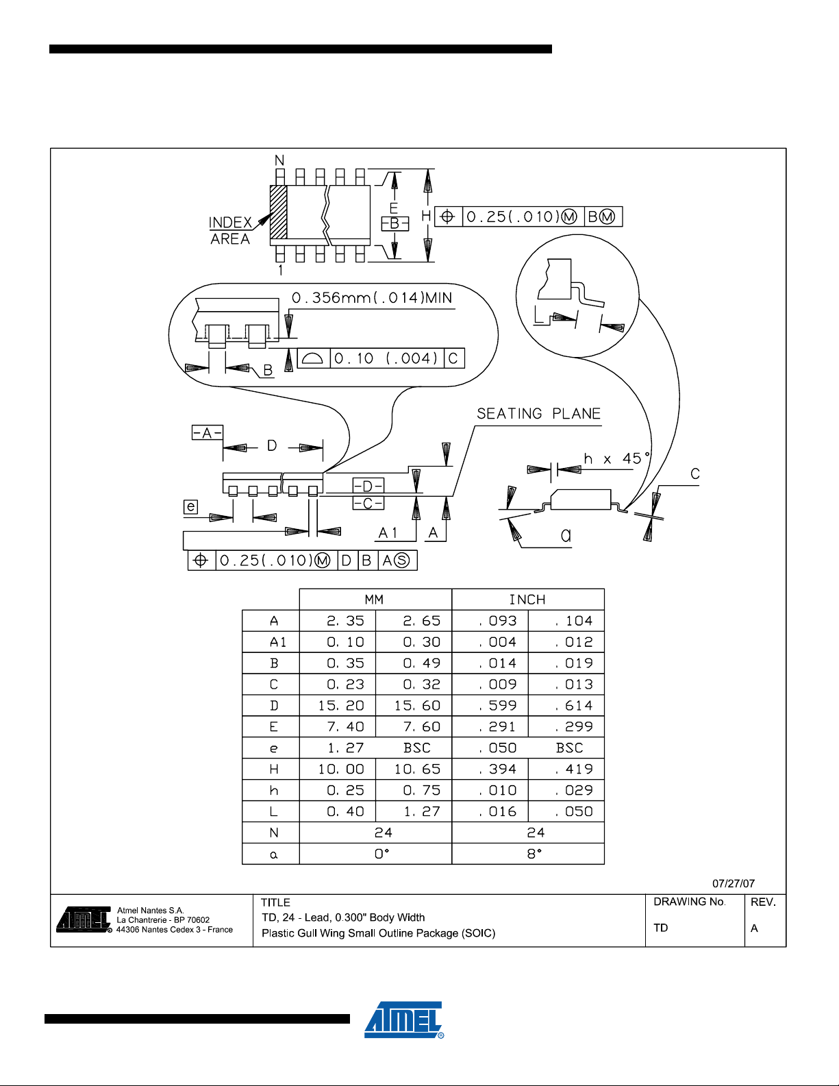
8.1 SO24
AT90PWM2/3/2B/3B
4317IS–AVR–01/08
19
Page 20

AT90PWM2/3/2B/3B
8.2 SO32
20
4317IS–AVR–01/08
Page 21

8.3 QFN32
AT90PWM2/3/2B/3B
4317IS–AVR–01/08
21
Page 22

22
AT90PWM2/3/2B/3B
4317IS–AVR–01/08
Page 23

9. Errata
9.1 AT90PWM2&3 Rev. A (Mask Revision)
• PGM: PSCxRB Fuse
• PSC: Prescaler
• PSC: PAOCnA and PAOCnB Register Bits (Asynchronous output control)
• PSC: PEVxA/B Flag Bits
• PSC: Output Polarity in Centered Mode
• PSC: Output Activity
• VREF
• DALI
• DAC: Register Update
• DAC: Output spikes
• DAC driver: Output Voltage linearity
• ADC: Conversion accuracy
• Analog comparator: Offset value
• Analog comparator: Output signal
• PSC: Autolock modes
• DALI: 17th bit detection
• PSC: One ramp mode with PSC input mode 8
AT90PWM2/3/2B/3B
1. PGM: PSCnRB Fuse
The use of PSCnRB fuse can make the parallel ISP fail.
Workaround:
When PSCnRB fuses are used, use the serial programming mode to load a new program
version.
2. PSC: Prescaler
The use of PSC's prescaler have the following effects :
It blocks the sample of PSC inputs until the two first cycles following the set of PSC run bit.
A fault is not properly transferred to other (slave) PSC.
Workaround:
Clear the prescaler PPREx bit when stopping the PSC (prun = 0), and set them to appropriate value when starting the PSC (prun = 1), these bits are in the same PCTL register
Do not use the prescaler when a fault on one PSC should affect other PSC’s
3. PSC: PAOCnA and PAOCnB Register Bits (Asynchronous output control)
These register bits are malfunctioning.
Workaround:
Do not use this feature.
4. PSC: PEVnA/B flag bits
These flags are set when a fault arises, but can also be set again during the fault itself.
Workaround:
Don't clear these flags before the fault disappears.
4317IS–AVR–01/08
23
Page 24

AT90PWM2/3/2B/3B
5. PSC: Output Polarity in Centered Mode
In centered mode, PSCOUTn1 outputs are not inverted, so they are active at the same time
as PSCOUTn0.
Workaround:
Use an external inverter (or a driver with inverting output) to drive the load on
PSCOUTn1.
6. PSC : POACnA/B Output Activity
These register bits are not implemented in rev A.
Workaround:
Do not use this feature.
7. VREF
Remark: To have Internal Vref on AREF pin select an internal analog feature such as DAC
or ADC.
Some stand by power consuption may be observed if Vref equals AVcc
8. DALI
Some troubles on Dali extension when edges are not symmetric.
Workaround:
Use an optocoupler providing symmetric edges on Rx and Tx DALI lines (only recommanded for software validation purpose).
9. DAC: Register Update
Registers DACL & DACH are not written when the DAC is not enabled.
Workaround:
Enable DAC with DAEN before writing in DACL & DACH. To prevent an unwanted zero output on DAC pin, enable DAC output, with DAOE afterwards.
10. DAC : Output spikes
During transition between two codes, a spike may appears
Work around:
Filter spike or wait for steady state
No spike appears if the 4 last signifiant bits remain zero.
11. DAC driver: Output Voltage linearity
The voltage linearity of the DAC driver is limited when the DAC output goes above Vcc - 1V.
Work around:
Do not use AVcc as Vref ; internal Vref gives good results
12. ADC : Conversion accuracy
The conversion accuracy degrades when the ADC clock is 1 & 2 MHz.
Work around:
When a 10 bit conversion accuracy is required, use an ADC clock of 500 kHz or below.
13. Analog comparator: Offset value
The offset value increases when the common mode voltage is above Vcc - 1.5V.
Work around:
Limit common mode voltage
14. Analog comparator: Output signal
24
4317IS–AVR–01/08
Page 25

AT90PWM2/3/2B/3B
The comparator output toggles at the comparator clock frequency when the voltage difference between both inputs is lower than the offset. This may occur when comparing signal
with small slew rate.
Work around:
This effect normally do not impact the PSC, as the transition is sampled once per PSC cycle
Be carefull when using the comparator as an interrupt source.
15. PSC : Autolock mode
This mode is not properly handled when CLKPSC is different from CLK IO.
Work around:
With CLKPSC equals 64/32 MHz (CLKPLL), use LOCK mode
16. DALI : 17th bit detection
17th bit detection do not occurs if the signal arrives after the sampling point.
Workaround:
Use this feature only for sofware development and not in field conditions
17. PSC : One ramp mode with PSC input mode 8
The retriggering is not properly handled in this case.
Work around:
Do not program this case.
18. PSC : Desactivation of outputs in mode 14
See “PSC Input Mode 14: Fixed Frequency Edge Retrigger PSC and Disactivate Output” on
page 155.
Work around:
Do not use this mode to desactivate output if retrigger event do not occurs during On-Time.
9.2 AT90PWM2B/3B
• PSC : Double End-Of-Cycle Interrupt Request in Centered Mode
• ADC : Conversion accuracy
1. PSC : Double End-Of-Cycle Interrupt Request in Centered Mode
2. ADC : Conversion accuracy
3. DAC Driver linearity above 3.6V
In centered mode, after the “expected” End-Of-Cycle Interrupt, a second unexpected Interrupt occurs 1 PSC cycle after the previous interrupt.
Work around:
While CPU cycle is lower than PSC clock, the CPU sees only one interrupt request. For PSC
clock period greater than CPU cycle, the second interrupt request must be cleared by
software.
The conversion accuracy degrades when the ADC clock is 2 MHz.
Work around:
When a 10 bit conversion accuracy is required, use an ADC clock of 1 MHz or below.
At 2 Mhz the ADC can be used as a 7 bits ADC.
With 5V Vcc, the DAC driver linearity is poor when DAC output level is above Vcc-1V. At 5V,
DAC output for 1023 will be around 5V - 40mV.
Work around: .
4317IS–AVR–01/08
25
Page 26

AT90PWM2/3/2B/3B
Use, when Vcc=5V, Vref below Vcc-1V.
Or, when Vref=Vcc=5V, do not uses codes above 800.
4. DAC Update in Autotrig mode
If the cpu writes in DACH register at the same instant that the selected trigger source occurs
and DAC Auto Trigger is enabled, the DACH register is not updated by the new value.
Work around: .
When using the autotrig mode, write twice in the DACH register. The time between the two
CPU writes, must be different than the trigger source frequency.
26
4317IS–AVR–01/08
Page 27

10. Datasheet Revision History for AT90PWM2/2B/3/3B
Please note that the referring page numbers in this section are referred to this document. The
referring revision in this section are referring to the document revision.
10.1 Changes from 4317A- to 4317B
1. PSC section has been rewritten.
2. Suppression of description of RAMPZ which does not exist.
10.2 Changes from 4317B- to 4317C
1. Added AT90PWM2B/3B Advance Information.
2. Various updates throughout the document.
10.3 Changes from 4317C- to 4317D
1. Update of Electrical and Typical Characteristics.
10.4 Changes from 4317D to 4317E
1. Changed product status from “Advanced Information” to “Preliminary”.
AT90PWM2/3/2B/3B
10.5 Changes from 4317E to 4317F
1. Remove JMP and CALL instruction in the Instruction Set Summary
2. Daisy chain of PSC input is only done in mode 7 - See “Fault events in Autorun mode”
on page 160.
3. Updated “Output Compare SA Register – OCRnSAH and OCRnSAL” on page 163
4. Updated “Output Compare RA Register – OCRnRAH and OCRnRAL” on page 163
5. Updated “Output Compare SB Register – OCRnSBH and OCRnSBL” on page 163
6. Updated “Output Compare RB Register – OCRnRBH and OCRnRBL” on page 164
7. Specify the “Analog Comparator Propagation Delay” - See “DC Characteristics” on
page 300.
8. Specify the “Reset Characteristics” - See “Reset Characteristics(1)” on page 47.
9. Specify the “Brown-out Characteristics” - See “Brown-out Characteristics(1)” on page
49.
10. Specify the “Internal Voltage Reference Characteristics - See “Internal Voltage Refer-
ence Characteristics(1)” on page 51.
10.6 Changes from 4317F to 4317G
1. Describe the amplifier operation for Rev B.
2. Clarify the fact that the DAC load given is the worst case.
3. Specify the ADC Min and Max clock frequency.
4. Describe the retrigger mode 8 in one ramp mode.
5. Specify that the amplifier only provides a 8 bits accuracy.
10.7 Changes from 4317G to 4317H
1. Updated “History” on page 2
2. Specify the “AREF Voltage vs. Temperature” on page 329
4317IS–AVR–01/08
27
Page 28

AT90PWM2/3/2B/3B
3. PSC : the Balance Flank Width Modulation is done On-Time 1 rather than On-Time 0
(correction of figures)
4. Updated “Maximum Speed vs. VCC” on page 303 (formulas are removed)
5. Update of the “Errata” on page 23
10.8 Changes from 4317H to 4317I
1. Updated “History” on page 2
2. Updated “Device Clocking Options Select AT90PWM2B/3B” on page 31
3. Updated “Start-up Times when the PLL is selected as system clock” on page 35
4. Updated “ADC Noise Canceler” on page 241
5. Updated “ADC Auto Trigger Source Selection for non amplified conversions” on page
250.
6. Added “ADC Auto Trigger Source Selection for amplified conversions” on page 250
7. Updated “Amplifier” on page 252
8. Updated “Amplifier 0 Control and Status register – AMP0CSR” on page 256
9. Updated “AMP0 Auto Trigger Source Selection” on page 257
10. Updated “Amplifier 1Control and Status register – AMP1CSR” on page 257
11. Updated “AMP1 Auto Trigger source selection” on page 258
12. Updated DAC “Features” on page 259 (Output Impedance)
13. Updated temperature range in “DC Characteristics” on page 300
14. Updated Vhysr in “DC Characteristics” on page 300
15. Updated “ADC Characteristics” on page 306
16. Updated “Example 1” on page 315
17. Updated “Example 2” on page 315
18. Updated “Example 3” on page 316
19. Added “I/O Pin Input HysteresisVoltage vs. VCC” on page 322
20. Updated “Ordering Information” on page 17
21. Added Errata for “AT90PWM2B/3B” on page 25
22. Updated Package Drawings “Package Information” on page 18.
23. Updated table on page 2.
24. Updated “Calibrated Internal RC Oscillator” on page 33.
25. Added “Calibrated Internal RC Oscillator Accuracy” on page 302.
26. Updated Figure 27-35 on page 329.
27. Updated Figure 27-36 on page 330.
28. Updated Figure 27-37 on page 330.
28
4317IS–AVR–01/08
 Loading...