BDTIC www.bdtic.com/ATMEL
Features
• High-performance, Low-power AVR
• Advanced RISC Architecture
– 133 Powerful Instructions – Most Single Clock Cycle Execution
– 32 x 8 General Purpose Working Registers + Peripheral Control Registers
– Fully Static Operation
– Up to 16 MIPS Throughput at 16 MHz
– On-chip 2-cycle Multiplier
• Non volatile Program and Data Memories
– 32K/64K/128K Bytes of In-System Reprogrammable Flash (AT90CAN32/64/128)
• Endurance: 10,000 Write/Erase Cycles
– Optional Boot Code Section with Independent Lock Bits
• Selectable Boot Size: 1K Bytes, 2K Bytes, 4K Bytes or 8K Bytes
• In-System Programming by On-Chip Boot Program (CAN, UART, ...)
• True Read-While-Write Operation
– 1K/2K/4K
– 2K/4K/4K Bytes Internal SRAM (AT90CAN32/64/128)
– Up to 64K Bytes Optional External Memory Space
– Programming Lock for Software Security
• JTAG (IEEE std. 1149.1 Compliant) Interface
– Boundary-scan Capabilities According to the JTAG Standard
– Programming Flash (Hardware ISP), EEPROM, Lock & Fuse Bits
– Extensive On-chip Debug Support
• CAN Controller 2.0A & 2.0B - ISO 16845 Certified
– 15 Full Message Objects with Separate Identifier Tags and Masks
– Transmit, Receive, Automatic Reply and Frame Buffer Receive Modes
– 1Mbits/s Maximum Transfer Rate at 8 MHz
– Time stamping, TTC & Listening Mode (Spying or Autobaud)
• Peripheral Features
– Programmable Watchdog Timer with On-chip Oscillator
– 8-bit Synchronous Timer/Counter-0
• 10-bit Prescaler
• External Event Counter
• Output Compare or 8-bit PWM Output
– 8-bit Asynchronous Timer/Counter-2
• 10-bit Prescaler
• External Event Counter
• Output Compare or 8-Bit PWM Output
• 32Khz Oscillator for RTC Operation
– Dual 16-bit Synchronous Timer/Counters-1 & 3
• 10-bit Prescaler
• Input Capture with Noise Canceler
• External Event Counter
• 3-Output Compare or 16-Bit PWM Output
• Output Compare Modulation
– 8-channel, 10-bit SAR ADC
• 8 Single-ended Channels
• 7 Differential Channels
• 2 Differential Channels With Programmable Gain at 1x, 10x, or 200x
– On-chip Analog Comparator
– Byte-oriented Two-wire Serial Interface
– Dual Programmable Serial USART
– Master/Slave SPI Serial Interface
• Programming Flash (Hardware ISP)
• Special Microcontroller Features
– Power-on Reset and Programmable Brown-out Detection
– Internal Calibrated RC Oscillator
– 8 External Interrupt Sources
– 5 Sleep Modes: Idle, ADC Noise Reduction, Power-save, Power-down & Standby
– Software Selectable Clock Frequency
– Global Pull-up Disable
• I/O and Packages
– 53 Programmable I/O Lines
– 64-lead TQFP and 64-lead QFN
• Operating Voltages: 2.7 - 5.5V
• Operating temperature: Automotive (-40°C to +125°C)
• Maximum Frequency: 8 MHz at 2.7V, 16 MHz at 4.5V
Bytes EEPROM (Endurance: 100,000 Write/Erase Cycles) (AT90CAN32/64/128)
®
8-bit Microcontroller
(1)
8-bit
Microcontroller
with
32K/64K/128K
Bytes of
ISP Flash
and
CAN Controller
AT90CAN32
AT90CAN64
AT90CAN128
Automotive
Summary
Note: 1. See details on Section 19.4.3 on page 241.
Rev. 7682CS–AUTO–04/08
1

1. Description
1.1 Comparison Between AT90CAN32, AT90CAN64 and AT90CAN128
AT90CAN32, AT90CAN64 and AT90CAN128 are all hardware and software compatible with
each other, the only difference is the memory size.
Table 1-1. Memory Size Summary
Device Flash EEPROM RAM
AT90CAN32 32K Bytes 1K Byte 2K Bytes
AT90CAN64 64K Bytes 2K Bytes 4K Bytes
AT90CAN128 128K Bytes 4K Byte 4K Bytes
1.2 Part Description
The AT90CAN32/64/128 is a low-power CMOS 8-bit microcontroller based on the AVR
enhanced RISC architecture. By executing powerful instructions in a single clock cycle, the
AT90CAN32/64/128 achieves throughputs approaching 1 MIPS per MHz allowing the system
designer to optimize power consumption versus processing speed.
The AVR core combines a rich instruction set with 32 general purpose working registers. All 32
registers are directly connected to the Arithmetic Logic Unit (ALU), allowing two independent
registers to be accessed in one single instruction executed in one clock cycle. The resulting
architecture is more code efficient while achieving throughputs up to ten times faster than conventional CISC microcontrollers.
The AT90CAN32/64/128 provides the following features: 32K/64K/128K bytes of In-System Programmable Flash with Read-While-Write capabilities, 1K/2K/4K bytes EEPROM, 2K/4K/4K
bytes SRAM, 53 general purpose I/O lines, 32 general purpose working registers, a CAN controller, Real Time Counter (RTC), four flexible Timer/Counters with compare modes and PWM, 2
USARTs, a byte oriented Two-wire Serial Interface, an 8-channel 10-bit ADC with optional differential input stage with programmable gain, a programmable Watchdog Timer with Internal
Oscillator, an SPI serial port, IEEE std. 1149.1 compliant JTAG test interface, also used for
accessing the On-chip Debug system and programming and five software selectable power saving modes.
The Idle mode stops the CPU while allowing the SRAM, Timer/Counters, SPI/CAN ports and
interrupt system to continue functioning. The Power-down mode saves the register contents but
freezes the Oscillator, disabling all other chip functions until the next interrupt or Hardware
Reset. In Power-save mode, the asynchronous timer continues to run, allowing the user to maintain a timer base while the rest of the device is sleeping. The ADC Noise Reduction mode stops
the CPU and all I/O modules except Asynchronous Timer and ADC, to minimize switching noise
during ADC conversions. In Standby mode, the Crystal/Resonator Oscillator is running while the
rest of the device is sleeping. Thi s allows very fast start-up combin ed with low po wer
consumption.
The device is manufactured using Atmel’s high-density nonvolatile memory technology. The Onchip ISP Flash allows the program memory to be reprogrammed in-system through an SPI serial
interface, by a conventional nonvolatile memory programmer, or by an On-chip Boot program
running on the AVR core. The boot program can use any interface to download the application
program in the application Flash memory. Software in the Boot Flash section will continue to run
while the Application Flash section is updated, providing true Read-While-Write operation. By
2
AT90CAN32/64/128
7682CS–AUTO–04/08

combining an 8-bit RISC CPU with In-System Self-Programmable Flash on a monolithic chip,
the Atmel AT90CAN32/64/128 is a powerful microcontroller that provides a highly flexible and
cost effective solution to many embedded control applications.
The AT90CAN32/64/128 AVR is supported with a full suite of program and system development
tools including: C compilers, macro assemblers, program debugger/simulators, in-circuit emulators, and evaluation kits.
1.3 Disclaimer
Typical values contained in this datasheet are based on simulations and characterization of
other AVR microcontrollers manufactured on the same process technology. Min and Max values
will be available after the device is characterized.
1.4 Automotive Quality Grade
The AT90CAN32/64/128 have been developed and manufactured according to the most stringent requirements of the international standard ISO-TS-16949 grade 1. This data sheet contains
limit values extracted from the results of extensive characterization (Temperature and Voltage).
The quality and reliability of the AT90CAN32/64/128 have been verified during regular product
qualification as per AEC-Q100.
AT90CAN32/64/128
As indicated in the ordering information paragraph, the products are available in three different
temperature grades, but with equivalent quality and reliability objectives. Different temperature
identifiers have been defined as listed in Table 1-2.
Table 1-2. Temperature Grade Identification for Automotive Products
Temperature Temperature
Identifier
-40 ; +85 T Similar to Industrial Temperature Grade but with
Automotive Quality
-40 ; +105 T1 Reduced Automotive Temperature Range
-40 ; +125 Z Full AutomotiveTemperature Range
Comments
7682CS–AUTO–04/08
3

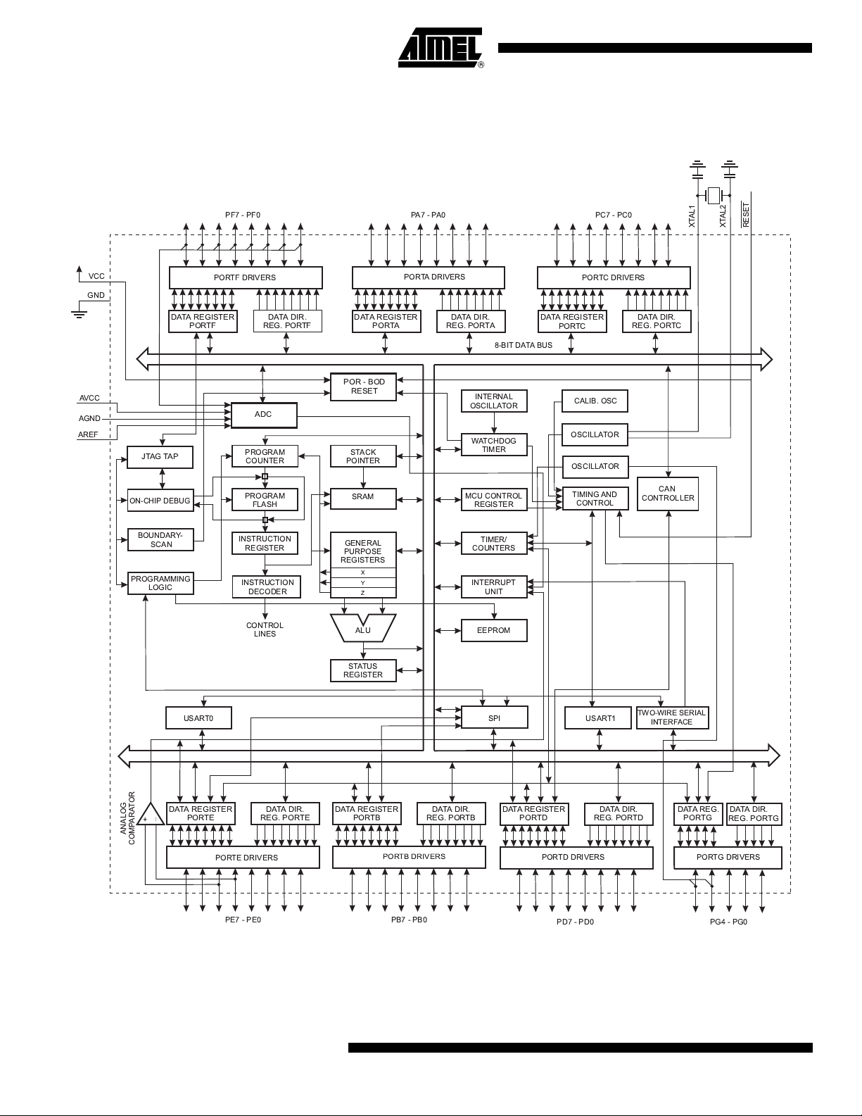
1.5 Block Diagram
PROGRAM
COUNTER
STACK
POINTER
PROGRAM
FLASH
MCU CONTROL
REGISTER
SRAM
GENERAL
PURPOSE
REGISTERS
INSTRUCTION
REGISTER
TIMER/
COUNTERS
INSTRUCTION
DECODER
DATA DIR.
REG. PORTB
DATA DIR.
REG. PORTE
DATA DIR.
REG. PORTA
DATA DIR.
REG. PORTD
DATA REGISTER
PORTB
DATA REGISTER
PORTE
DATA REGISTER
PORTA
DATA REGISTER
PORTD
INTERRUPT
UNIT
EEPROM
SPIUSART0
STATUS
REGISTER
Z
Y
X
ALU
PORTB DRIVERS
PORTE DRIVERS
PORTA DRIVERS
PORTF DRIVERS
PORTD DRIVERS
PORTC DRIVERS
PB7 - PB0PE7 - PE0
PA7 - PA0PF7 - PF0
RESET
VCC
AGND
GND
AREF
XTAL1
XTAL2
CONTROL
LINES
+
-
ANALOG
COMPARATOR
PC7 - PC0
INTERNAL
OSCILLATOR
WATCHDOG
TIMER
8-BIT DATA BUS
AVCC
USART1
TIMING AND
CONTROL
OSCILLATOR
OSCILLATOR
CALIB. OSC
DATA DIR.
REG. PORTC
DATA REGISTER
PORTC
ON-CHIP DEBUG
JTAG TAP
PROGRAMMING
LOGIC
BOUNDARY-
SCAN
DATA DIR.
REG. PORTF
DATA REGISTER
PORTF
ADC
POR - BOD
RESET
PD7 - PD0
DATA DIR.
REG. PORTG
DATA REG.
PORTG
PORTG DRIVERS
PG4 - PG0
TWO-WIRE SERIAL
INTERFACE
CAN
CONTROLLER
Figure 1-1. Block Diagram
4
AT90CAN32/64/128
7682CS–AUTO–04/08

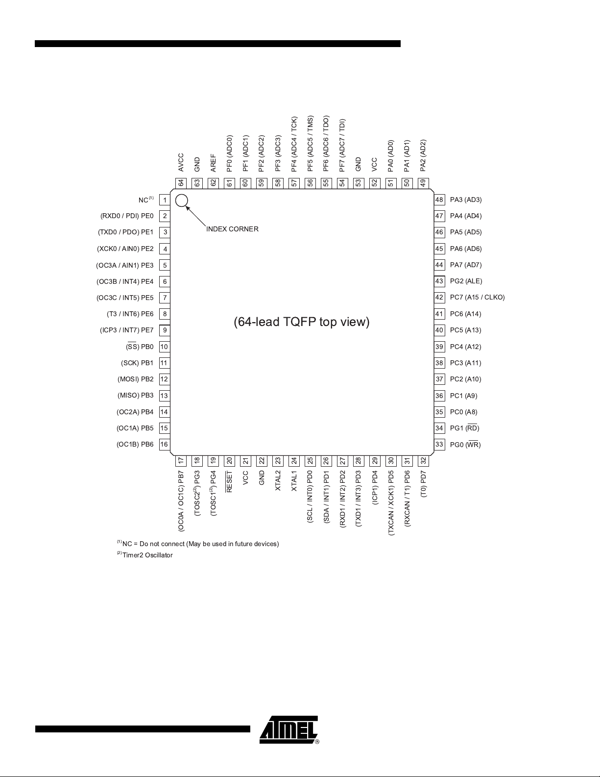
1.6 Pin Configurations
PC0 (A8)
VCC
GND
PF0 (ADC0)
PF7 (ADC7 / TDI)
PF1 (ADC1)
PF2 (ADC2)
PF3 (ADC3)
PF4 (ADC4 / TCK)
PF5 (ADC5 / TMS)
PF6 (ADC6 / TDO)
AREF
GND
AVCC
17
61
60
18
592058
19
21
572256
235524
54
25
532652
27
51
29
28
50
49
32
31
30
(RXD0 / PDI) PE0
(TXD0 / PDO) PE1
(XCK0 / AIN0) PE2
(OC3A / AIN1) PE3
(OC3B / INT4) PE4
(OC3C / INT5) PE5
(T3 / INT6) PE6
(ICP3 / INT7) PE7
(SS) PB0
(SCK) PB1
(MOSI) PB2
(MISO) PB3
(OC2A) PB4
(OC0A / OC1C) PB7
(TOSC2 ) PG3
(OC1B) PB6
(TOSC1 ) PG4
(OC1A) PB5
PC1 (A9)
(T0) PD7
PC2 (A10)
PC3 (A11)
PC4 (A12)
PC5 (A13)
PC6 (A14)
PC7 (A15 / CLKO)
PA7 (AD7)
PG2 (ALE)
PA6 (AD6)
PA5 (AD5)
PA4 (AD4)
PA3 (AD3)
PA0 (AD0)
PA1 (AD1)
PA2 (AD2)
(RXCAN / T1) PD6
(TXCAN / XCK1) PD5
(ICP1) PD4
(TXD1 / INT3) PD3
(RXD1 / INT2) PD2
(SDA / INT1) PD1
(SCL / INT0) PD0
XTAL1
XTAL2
RESET
GND
VCC
PG1 (RD)
PG0 (WR)
2
3
1
4
5
6
7
8
9
10
11
12
13
14
16
15
64
63
62
47
46
48
45
44
43
42
41
40
39
38
37
36
35
33
34
(2)
(2)
NC = Do not connect (May be used in future devices)
(1)
Timer2 Oscillator
(2)
NC
(1)
(64-lead TQFP top view)
INDEX CORNER
Figure 1-2. Pinout AT90CAN32/64/128 - TQFP
AT90CAN32/64/128
7682CS–AUTO–04/08
5
 Loading...