

Page 1

AT89STK-11 Starter Kit
..............................................................................................
Hardware User Guide
Page 2

Table of Contents
Section 1
Introduction ........................................................................................... 1-1
1.1 Features ....................................................................................................1-1
1.2 Supported Devices....................................................................................1-2
Section 2
Hardware Description ........................................................................... 2-4
2.1 Board Overview.........................................................................................2-4
2.2 Block Diagram...........................................................................................2-5
2.3 Power Supply ............................................................................................2-5
2.4 Reset.........................................................................................................2-6
2.5 Features ....................................................................................................2-7
2.6 Interfaces ..................................................................................................2-7
2.7 Board Settings ..........................................................................................2-9
Section 3
ISP Programming ............................................................................... 3-12
3.1 Manual ISP Mode ...................................................................................3-12
3.2 Auto ISP Mode ........................................................................................3-12
3.3 FLIP Software .........................................................................................3-13
3.4 Batchisp Software ...................................................................................3-13
Section 4
Appendix A: Board Layout .................................................................. 4-14
Appendix B: Bill of Materials ............................................................... 4-15
4.1 Bill of Materials Table..............................................................................4-15
Appendix C: Board Schematics .......................................................... 4-17
Appendix D: References/Acronyms .................................................... 4-22
4.2 References..............................................................................................4-22
4.3 Acronyms ................................................................................................4-22
AT89STK-11 Hardware User Guide 1
7676B–8051–08/07
Page 3

Section 1
Introduction
This document describes the AT89STK-11 board dedicated to the standard C51 microcontrollers with in-system programming.
All of the microcontroller I/Os are made available in an expansion area with prototyping
facilities.
1.1 Features
Stand-alone Board
In-System Programmable (ISP) including ‘Auto ISP’ feature
On-board Voltage Regulator
Microcontroler on its sockets
– PLCC44-pin package
On-board 3V or 5V power supply circuitry
– from an external power connector
– from an external battery
On-board RESET
Leds : Power, ALE, RS232 Rx and Tx
External MCU clock connector
External PCA clock connector
TWI, SPI and RS232 connectors
INT0 & INT1 Push-button
Expansion area with prototyping facilities
Commercial Temperature Range: 0 to +70°C Operating Temperature
Dimension: 95 mm x 120 mm
AT89STK-11 Hardware User Guide 1-1
7676B–8051–08/07
Page 4

Introduction
1.2 Supported Devices
AT89C51RE2
AT89C51RB2
AT89C51RC2/IC2
AT89C51RD2/ID2/ED2
AT89STK-11 Hardware User Guide 1-2
7676B–8051–08/07
Page 5
Section 2
Hardware Description
2.1 Board Overview
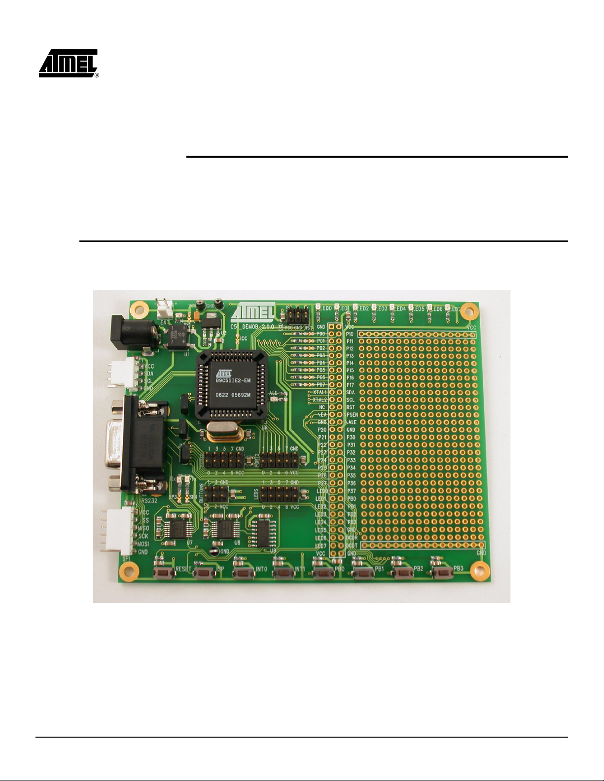
Figure 2-1 shows the AT89STK-11 board.
Figure 2-1. AT89STK-11
This photo is not contractual and may be modified without notification by Atmel.
AT89STK-11 Hardware User Guide 2-4
7676B–8051–08/07
Page 6
Hardware Description
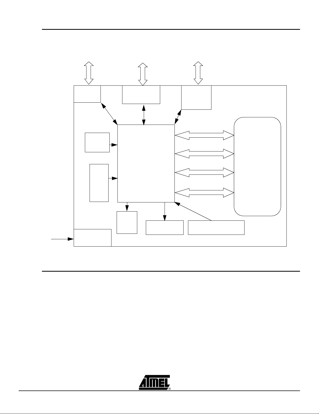
Power Supply
Full UART
External
Power
PC Host
C51
P2
P3
EA
RST
ISP
Expansion
TWI
P0
P1
SPI
INT0
Leds:
PWR
ALE
16MHz
Quartz
PLCC44
3V or 5V
INT1
Area
User LEDs User Push Buttons
2.2 Block Diagram
Figure 2-2. Block Diagram of AT89STK-11
Figure 2-2 shows the functional block diagram of the AT89STK-11, with the I/O usage.
2.3 Power Supply
2.3.1 Power Supply Sources
2.3.1.1 JACK PWR Connector
The on-board power supply circuitry allows various power supply configurations. This
gives the user the capability to power the devices in the 3V and in the 5V voltage range.
The power supply source can come from two different and exclusive sources:
either from the JACK PWR connector
either from the 2-point sip EXT connector.
The Jack power connector implemented on board is a female Jack connector with internal 2.1mm conductor. It requires a male JACK outlet with 2.1mm capability.
No specific polarization is mandatory as on-board diode rectifier gives a protection
against inadvertent polarization invertion.
When using the JACK power supply, the board is powered with a 5V voltage.
2-5 AT89STK-11 Hardware User Guide
7676B–8051–08/07
Page 7
Hardware Description
Figure 2-3. Male JACK Outlet and Wires
Note: Do not mount more than one power supply source on AT89STK-11 Board.
Note: There is a diode voltage level between the negative output of the power supply
and the “GND”. This could introduce some voltage gap during measurement
and instrumentation.
2.3.1.2 External EXT connector
The battery power connector implemented on board is a male two point SIP connector.
It requires an external power cable with a female 2 points connector.
When powered though this interface, polarization is mandatory as no protection is given
on board.
The EXT power supply circuitry support input supply from 2.7V up to 5.5V DC.
Figure 2-4. EXT PWR Female Connector / Cable
Note: Do not mount more than one power supply source on board.
Note: Keep SP1 closed when using the EXT input
2.4 Reset
To be compatible with Atmel microcontrollers which have (or not) its on-chip RESET circuitry (c.f.microcontroller datasheet), the board provides a RESET signal witch can
come from 2 different sources:
2.4.1 Power-on RESET The on-board RC network acts as power-on RESET.
2.4.2 RESET Push Button By pressing the RESET push button on the board, a warm RESET of the microcontroller
is performed.
AT89STK-11 Hardware User Guide 2-6
7676B–8051–08/07
Page 8

Hardware Description
2.5 Features
This section presents the various features such as leds, buttons, etc... available on the
board.
2.5.1 Push-Buttons RESET can be used to apply warm reset to the MCU
ISP can be used with RESET to apply hardware conditions resulting in bootloader
start
INT0 push-button can be used to activate INT0 input
INT1 push-button can be used to activate INT1 input
2.5.2 User Push buttons PB0, PB1, PB2 and PB3 are four push-buttons available for user application
They are made available on a 6 pins socket and in the expansion area so user can use
them according to the application needs.
2.5.3 Indicator LEDs PWR led is driven by input of voltage regulator
Rx led is connected to Rx of UART MCU (SP3 jumper can be soldered or not)
Tx led is connected to Tx of UART MCU (SP4 jumper can be soldered or not)
ALE led is connected to ALE of MCU
2.5.4 User LEDs LED0, LED1, ... LED7 are height leds available for user application
They are made available on a 10 pins socket and in the expansion area so user can use
them according to its application needs.
2.5.5 Ports Port 0 and Port 2 are made available on two 10 pins sockets to ease user interconnec-
tion to the MCU.
The are also available on the expansion area.
2.5.6 Clocks An external clock can be connected to the board to control externally XTAL1 input clock
of MCU by using the XTAL1 from the expansion area.
In the same way, another external clock can be connected to control externally the PCA
clock (P1.2/ECI).
2.6 Interfaces
2.6.1 TWI The TWI connector is controlled by hardware TWI I/O of MCU (for Product including this
feature). The signals sda and scl are controlled by the TWI ports of MCU.
This TWI bus is also connected to the expansion area.
External TWI pull-ups are not provided on the AT89STK-11.
2.6.2 SPI The SPI connector is directly connected to SPI I/O of the MCU.
2.6.3 RS-232 The DB9 connector is connected to on-chip UART peripheral through a standard RS232
driver/receiver. Two leds are provided to indicate activity on Rx and Tx lines (They can
be disconnected removing solder pad SP3 and SP4).
2.6.4 OCD The On-Chip Debug interface (OCD) is provided on a 6-pin connector.
2-7 AT89STK-11 Hardware User Guide
7676B–8051–08/07
Page 9

Hardware Description
This interface enables the debug of the application through ATMEL OCD dongle for
AT89C51RE2/IE2/RD3/IE3 only.
2.6.5 Expansion Area In addition to a 16x29 pad array, two rows of pads are given on the right side of the
board to offer all the MCU signals tu user application. Any application expansion can be
built on board through this interface.
2.7 Board Settings
The C51 Demo Board has the following settings:
Jumpers
Solder straps
Test points
2.7.1 Jumpers The following table provides an overview of the jumpers, the solder straps and their
default configuration.
Table 2-1. Jumpers and Switches Overview
Reference PCB Label Function Default
Jumper J11 J11 RTS of RS232 OFF
Jumper J12 J12 DTR of RS232 OFF
Jumper J13 J13 OFF
Figure 2-5. Jumper Setting Definition
2.7.2 Solder Straps Solder straps allow to modify the board configuration for specific usage.
Table 2-2. Solder Straps Overview
Reference PCB Label Function Default
Solder strap SP1 SP1 External Power Supply Isolation Soldered
Solder strap SP2 ICC Consumption measurement Soldered
Solder strap SP3 SP3 Rx Led Soldered
Solder strap SP4 SP4 Tx Led Soldered
AT89STK-11 Hardware User Guide 2-8
7676B–8051–08/07
Page 10

Hardware Description
2.7.3 Test Points
Figure 2-6. Solder Strap Definition
Test points are used to check the internal power supply of the microcontroller.
Table 2-3. Table of Test Points
Reference PCB Label Function
TP1 VCC
TP2,TP3 GND Test point for GND
Test point for Vcc
2-9 AT89STK-11 Hardware User Guide
7676B–8051–08/07
Page 11

Section 3
ISP Programming
The On-Chip memories and configuration bytes can be programmed using the ISP
mode of the device and Atmel's FLexible In-system Programmer Software (FLIP)
described below.
3.1 Manual ISP Mode See Section “FLIP Software”, page 11.
3.1.1 Board Configuration To use ISP mode, no specific configuration is necessary on the board. Only make sure
that the EA pin of the product is tied to Vcc (internal code execution only).
3.1.2 Operating Mode To enter in ISP mode, press both the RESET and ISP buttons simultaneously.
First release the RESET button and then the ISP button. The device enters in
ISP mode.
3.2 Auto ISP Mode
3.2.1 Board Configuration To use Auto ISP mode, put the board in the same configuration as ISP mode and also:
AT89STK-11 Hardware User Guide 3-10
It allows the host PC application (Atmel Flip software for example) to control the hardware conditions from the serial lines RTS and DTR.
Thus with the Auto ISP mode, the user does not need to push the ISP and RESET
buttons.
Close RTS (J11) jumper
Close DTR (J12) jumper
7676B–8051–08/07
Page 12

ISP Programming
3.3 FLIP Software
3.4 Batchisp Software
FLIP software runs on Windows® and Linux® Operating Systems. FLIP supports in-system programming of Flash C51 devices through RS232. The latest version of FLIP
software can be downloaded from the Atmel web site, www.atmel.com.
Batchisp is an In-System Programming application which can perform the same operations as FLIP but is designed to be launched from the DOS command window.
The main purpose of batchisp is to automate ISP operations on several parts. It may
also be launched from an IDE like Keil's uVision®2 one : you can compile and link your
embedded program, generate the HEX file and download it to the target hardware without leaving the Keil's IDE. This makes embedded software development and test faster.
Autoisp function is an operation which allows to enter in ISP mode without any hardware
handling.This is done thanks to DTR and RTS RS232 signals which can control on the
Board the RST and PSEN I/O of MCU.
3-11 AT89STK-11 Hardware User Guide
7676B–8051–08/07
Page 13

Figure 4-1. Board Components View Diagram
Section 4
Appendix A: Board Layout
AT89STK-11 Hardware User Guide 4-12
7676B–8051–08/07
Page 14

Appendix B: Bill of Materials
4.1 Bill of Materials Table
Item Q.ty Reference Part Tech. Caracteristics Package Manufacturer
1
2 1 C1 1µF 10Vmin ±10% Case A AVX
3 2 C14,C15 22pF 10Vmin ±10%
4 1 D1 Red Led I=10 mA Agilent
5 11 D2,D3,D4,D5,D6,D7,D8,D9,
6 1 J1 SIP2 SOCKET . Pitch 2.54mm Molex
7 1 J2 CONNECTOR JACK PWR Int.Diam=2.1mm
8 1 J3 HEADER 31x2/SM
9 2 J4,J8 HEADER 3X2 BARRETTE SECABLE Pitch 2.54mm Tyco Elec. / AMP
10 3 J5,J6,J10 HEADER 5X2 BARRETTE SECABLE Pitch 2.54mm Tyco Elec. / AMP
11 1 J7 CONNECTOR SIP6 RA . . .
12 1 J9 SIP4 . . .
13 3 J11,J12,J13 JUMPER Pitch 2.54mm Tyco™ Elec. / AMP
13bis 3 JUMPER shunt Pitch 2.54mm Arwin
14 1 P1 SUB-D9 FEMALE 90° with harpoons Tyco Elec. / AMP
15 1 R1 270 1/16W-5% SMD Case 0603 Multicomp
16
17 1 R3 820 1/16W-5% SMD Case 0603 Multicomp
18 8 R4,R6,R8,R9,R10,R11,R12,
19 4
20 8 SW1,SW2,SW3,SW4,SW5,SW6,
CD1,CD2,C2,CD3,C3,C4,
CD5,C5,CD6,C6,CD7,C7,C8,
29
C9,C10,C11,C12,C13,C16,
C17,C18,C19,C20,C21,C22,
C23,C24,C25,C26
D10,D11,D12
R2,R5,R14,R15,R16,R17,
14
R24
R13
SP1,SP2,SP3,SP4,SP5, SP6,
SP7, SP8, SP9, SP10, SP11,
SP12
SW7,SW8
100n 50V-10% Ceramic CASE 0805 PHYCOMP
EIA/IECQ
3216
Green Led I=10 mA Agilent
Int. Diam.
2.1mm
1K 0.06W, 5% Case 0603 MulticompR18,R19,R20,R21,R22,R23,
10k 0.06W, 5% Case 0603 Multicomp
SolderPad
PUSH-BUTTON SMD, rectangular See DS ITT Canon
PHYCOMP
®
®
®
Cliff
®
AT89STK-11 Hardware User Guide 4-13
7676B–8051–08/07
Page 15
Appendix B: Bill of Materials
Item Q.ty Reference Part Tech. Caracteristics Package Manufacturer
21 3 TP1,TP2,TP3 TEST POINT Through Hole Pad Hole 1.1mm Vero
22 1 U1 DF005S TO269AA Vishay
23 1 U2 LM317 SOT-223 National
25 1 U6 AT8xC51_PLCC44 Socket
25bis 1 U6 AT8xC51_PLCC44
26 2 U7,U8 SIPEX-SP3232ECA Ref=SP3232ECA SSOP16 Maxim
27 1 U9 74HC125/SO SOIC texas
28 1 Y1 CRYSTAL HC49 . .
28bis 2 Y1 CRYSTAL tulip . .
29 8
R100, R101, R102, R103,
R104, R105, R106, R107
4,7K 0.06W, 5% Case 0603 Multicomp
®
®
®
AT89STK-11 Hardware User Guide 4-14
7676B–8051–08/07
Page 16

Appendix C: Board Schematics
AT89STK-11 Hardware User Guide 4-15
7676B–8051–08/07
Page 17
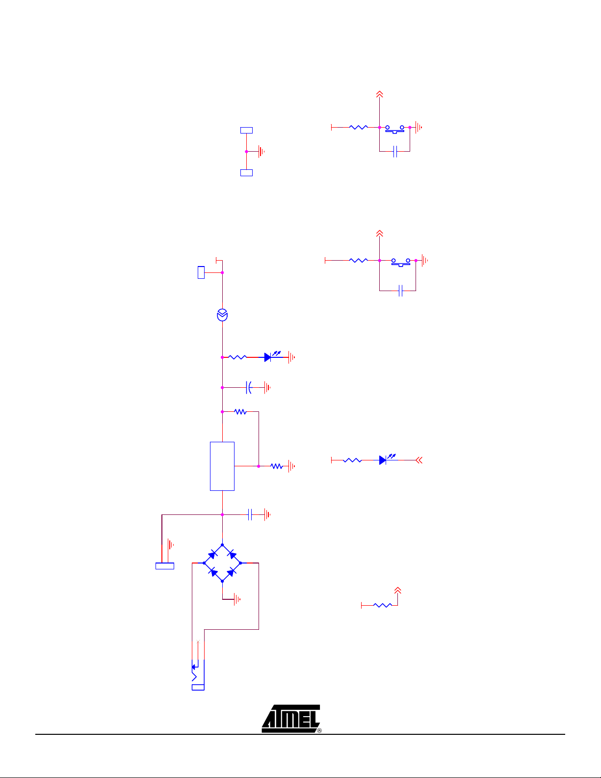
Figure 4-2. AT89STK-11 Schematics (1 of 4)
P3.3/INT1P3.2/INT0
Vcc
Vcc
Vcc
Vcc
Vcc
/EA
P3_2/INT0
/ALE
P3_3/INT1
Default State : Closed
R21KR2
1K
CD5
100n
CD5
100n
R3
820R3820
R8
10KR810K
Vin Vout
ADJ
U2
LM317EMP/SOT223
SOT223
U2
LM317EMP/SOT223
SOT223
R4
10KR410K
1
TP1 Vcc TPTP1 Vcc TP
D2
ALED2ALE
1
TP3TP3
1
2
J1
SIP2 SOCKET
Alternate Power Supply
J1
SIP2 SOCKET
Alternate Power Supply
1
3
2
4
- +
U1
DF005S
- +
U1
DF005S
1
TP2
GND TP
TP2
GND TP
SW3
INT1
SW3
INT1
SW2
INT0
SW2
INT0
CD3
100n
CD3
100n
SP1SP1
R9
10KR910K
D1
PowerD1Power
R1
270R1270
R51KR5
1K
CD1
100n
CD1
100n
321
J2
CONNECTOR JACK PWR
Power Supply
J2
CONNECTOR JACK PWR
Power Supply
C1
1µFC11µF
Appendix C: Board Schematics
AT89STK-11 Hardware User Guide 4-16
7676B–8051–08/07
Page 18
Appendix C: Board Schematics
Vss
Vcc
Vcc
Vcc
Vcc Vcc
Vcc Vcc Vcc Vcc Vcc Vcc Vcc Vcc
Vcc Vcc Vcc Vcc
Vcc
Vcc
Vcc
P1.1/T2EX/SS
P1.5/CEX2/MISO
P1.7/CEX4/MOSI
P1.6/CEX3/SCK
P0_0
P0_2
P0_4
P0_6
P0_1
P0_3
P0_5
P0_7P2_6
P2_0
P2_2
P2_4
P2_1
P2_3
P2_5
P2_7
LED_0
LED_1
LED_2
LED_3
LED_4
LED_5
LED_6
LED_7
PB_0 PB_1 PB_2 PB_3
LED_6
LED_1
LED_3
LED_5
LED_7
LED_0
LED_2
LED_4
PB_2
PB_0 PB_1
PB_3
TWI_hard_scl
TWI_hard_sda
OCD_Rx
OCD_Tx
/PSEN
RST
Port P0 Port P2
LEDs
Buttons
OCD
TWI
C11 100nC11 100n
R191KR19
1K
R10
10k
R10
10k
C5 100nC5 100n
D6D6
246810
13579
J5
HEADER 5X2
J5
HEADER 5X2
C6
100nC6100n
246
135
J4
HEADER 3X2
J4
HEADER 3X2
R201KR20
1K
D3D3
C2
100nC2100n
D7D7 D10D10
SW7SW7
R211KR21
1K
246810
13579
J10
HEADER 5X2
J10
HEADER 5X2
D5D5
R161KR16
1K
R151KR15
1K
246810
13579
J6
HEADER 5X2
J6
HEADER 5X2
R141KR14
1K
C9
100nC9100n
R13
10k
R13
10k
SW6SW6
C7
100nC7100n
SW5SW5
123
4
J9
SIP4J9SIP4
C8
100nC8100n
C10
100n
C10
100n
D9D9
C4
100nC4100n
D8D8
C3
100nC3100n
C12
100n
C12
100n
246
135
J8
HEADER 3X2
J8
HEADER 3X2
R11
10k
R11
10k
R181KR18
1K
R171KR17
1K
SW4SW4
R12
10k
R12
10k
12345
6
J7
SPI Male
J7
SPI Male
D4D4
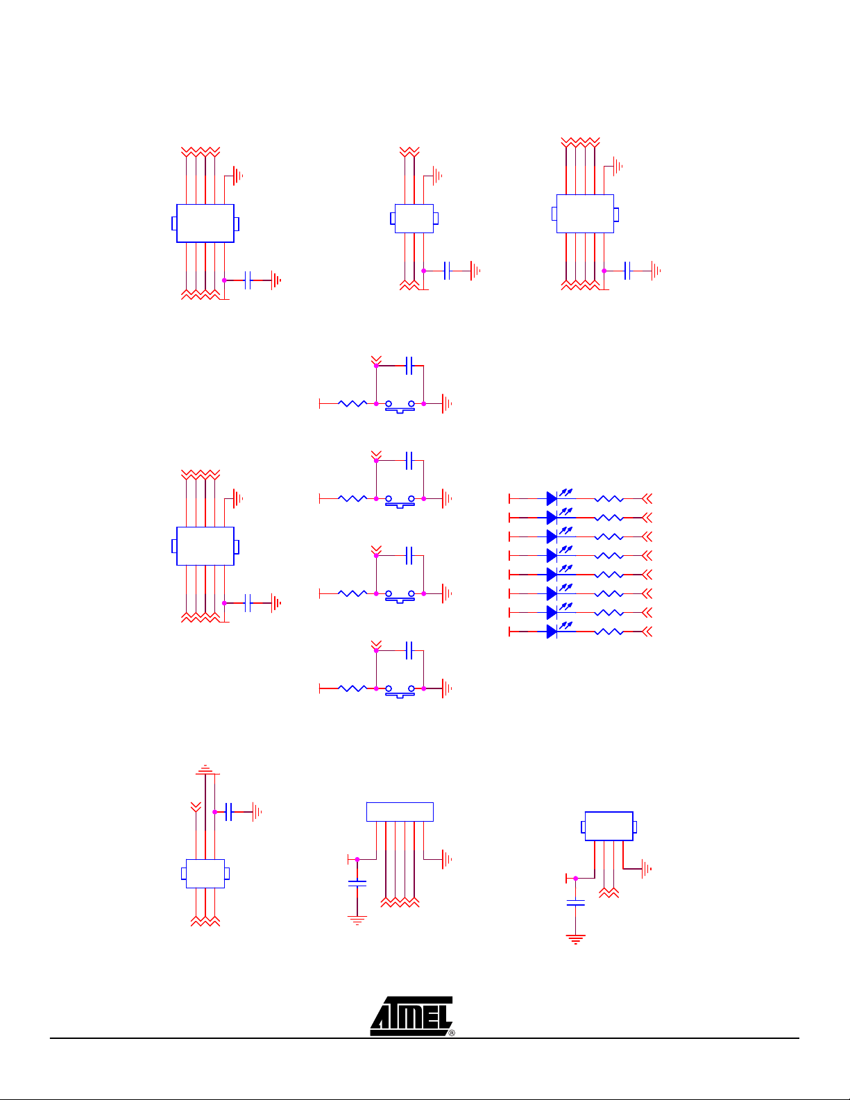
Figure 4-3. AT89STK-11 Schematics (2 of 4)
4-17 AT89STK-11 Hardware User Guide
7676B–8051–08/07
Page 19

Figure 4-4. AT89STK-11 Schematics (3 of 4)
XTAL2
XTAL1
VccVcc_cpu
Vcc_cpuVcc
Vcc
Vcc
P0_0
P0_1
P0_2
P0_3
P0_4
P0_5
P0_6
P0_7
P1.0/T2
P1.1/T2EX/SS
P1.2/ECI
P1.3/CEX0
P1.4/CEX1
P1.6/CEX3/SCK
P1.7/CEX4/MOSI
P2_0
P2_1
P2_2
P2_3
P2_4
P2_5
P2_6
P2_7
P3_0/RxD
P3_1/TxD
P3_2/INT0
P3_3/INT1
P3_4
P3_5
P3_6
P3_7
/ALE
/PSEN
/EA
RST
TWI_hard_sda
TWI_hard_scl
P1.5/CEX2/MISO
OCD_Rx
OCD_Tx
XTAL1
XTAL2
P0_0
P0_1
P0_2
P0_3
P0_4
P0_5
P0_6
P0_7
TWI_hard_scl
TWI_hard_sda
/EA
XTAL1
XTAL2
/ALE
P0_0
P0_1
P0_2
P0_3
P0_4
P0_5
P0_6
P0_7
OCD_Rx
OCD_Tx
RST
P1.0/T2
P1.1/T2EX/SS
P1.2/ECI
P1.3/CEX0
P1.4/CEX1
P1.5/CEX2/MISO
P1.6/CEX3/SCK
P1.7/CEX4/MOSI
/PSEN
P3_0/RxD
P3_1/TxD
P3_2/INT0
P3_3/INT1
P3_4
P3_5
P3_6
P3_7
PB_1
PB_0
PB_3
PB_2
LED_6
LED_1
LED_3
LED_5
LED_7
P2_0
P2_1
P2_2
P2_3
P2_4
P2_5
P2_6
P2_7
LED_0
LED_2
LED_4
Expansion Connector
R105 4.7KR105 4.7K
R104 4.7KR104 4.7K
Y1Y1
R103 4.7KR103 4.7K
SP6SP6
RST
10
XTAL2
20
XTAL1
21
GND
22
PSEN
32
ALE/PROG
33
EA/VPP
35
VCC
44
P1.02P1.13P1.24P1.35P1.46P1.57P1.68P1.7
9
P2.0/A824P2.1/A9
25
P2.2/A1026P2.3/A1127P2.4/A1228P2.5/A1329P2.6/A1430P2.7/A15
31
P3.0/RXD
11
P3.1/TXD
13
P3.2/INT0
14
P3.3/INT1
15
P3.4/T016P3.5/T1
17
P3.6/WR
18
P3.7/RD
19
P0.0/AD0
43
P0.1/AD1
42
P0.2/AD2
41
P0.3/AD3
40
P0.4/AD4
39
P0.5/AD5
38
P0.6/AD6
37
P0.7/AD7
36
Rx_OCD
1
RxD_1/SDA
12
TxD_1/SCL
34
Tx_OCD
23
U6
AT8xC51_PLCC44
U6
AT8xC51_PLCC44
R102 4.7KR102 4.7K
SP2SP2
R101 4.7KR101 4.7K
C13
100n
C13
100n
R100 4.7KR100 4.7K
SP12SP12
SP11SP11
CD6
100n
CD6
100n
CD7
100n
CD7
100n
C15
22pF
C15
22pF
C14
22pF
C14
22pF
2468101214161820222426283032343638404244464850525456586062
13579
11131517192123252729313335373941434547495153555759
61
J3
HEADER 31x2/SM
J3
HEADER 31x2/SM
SP8SP8
R107 4.7KR107 4.7K
SP10SP10
SP7SP7
R106 4.7KR106 4.7K
SP9SP9
SP5SP5
Appendix C: Board Schematics
AT89STK-11 Hardware User Guide 4-18
7676B–8051–08/07
Page 20

Appendix C: Board Schematics
DSR
Vcc
RTS
Rx_PC
CTS
CTS RTS
Tx_MCU
DTR
Tx_PC
Rx_MCU
Vcc
Vcc
Vcc
Vcc
Vcc
Vcc
Vcc
Vcc
P3_0/RxD
P3_1/TxD
/PSEN
RST
"grain de café""grain de café"
Vcc
SP4SP4
C26
100n
C26
100n
CD2
100n
CD2
100n
C16
100n
C16
100n
C23
100n
C23
100n
SW1
RESET
SW1
RESET
R221KR22
1K
2 3
14
1
7
U9A
74HC125/SO_5
U9A
74HC125/SO_5
SP3SP3
C21
100n
C21
100n
1 2
J11
RTS
J11
RTS
R241KR24
1K
C22
100n
C22
100n
SW8
ISP
SW8
ISP
R231KR23
1K
C18
100n
C18
100n
C17
100n
C17
100n
C25
100n
C25
100n
5 6
14
4
7
U9B
74HC125/SO_5
U9B
74HC125/SO_5
1 2
J13J13
C20
100n
C20
100n
C1+1C1-3C2+4C2-
5
VCC
16
GND
15
V+
2V-6
R1OUT12R2OUT
9
T1IN11T2IN
10
R1IN13R2IN
8
T1OUT14T2OUT
7
U8
SIPEX-SP3232ECA
U8
SIPEX-SP3232ECA
1 2
J12
DTR
J12
DTR
D11
Green Led
Rx LED
D11
Green Led
Rx LED
R6
10KR610K
C24
100n
C24
100n
C1+1C1-3C2+4C2-
5
VCC
16
GND
15
V+
2V-6
R1OUT12R2OUT
9
T1IN11T2IN
10
R1IN13R2IN
8
T1OUT14T2OUT
7
U7
SIPEX-SP3232ECA
U7
SIPEX-SP3232ECA
C19
100n
C19
100n
594837261
P1
SUB-D9 FEMALE
RS232
P1
SUB-D9 FEMALE
RS232
D12
Green Led
Tx LED
D12
Green Led
Tx LED
Figure 4-5. AT89STK-11 Schematics (4 of 4)
4-19 AT89STK-11 Hardware User Guide
7676B–8051–08/07
Page 21

Appendix D: References/Acronyms
4.2 References
4.3 Acronyms
AT89C51RD2/ID2/ED2/RB2/RC2/IC2/RE2/IE2 and AT89C51RD3/IE3 Product
Datasheet.
FLIP: FLexible In-system Programming
ISP: In-System programming
AT89STK-11 Hardware User Guide 4-20
7676B–8051–08/07
Page 22

Appendix D: References/Acronyms
Document Revision History
Changes from 7676A to 7676B
1. Section 1.2, page 1-2 : AT89C51RE3/ID3/IE2 not supported.
2. Section 2.3.1.2, page 2-5 : SP1 must be kept closed.
3. Section 3.1.1, page 3-11 : SW1 switch and EA jumper do not exist.
4. Appendix A, page 4-13 : the given board layout was wrong. Replaced by the
right one.
5. Appendix C, page 4-19 : there was an error on page 4 of the schematic.
Pin5 of U9B is now connected to Vcc instead of GND.
4-21 AT89STK-11 Hardware User Guide
7676B–8051–08/07
Page 23

Atmel Corporation Atmel Operations
2325 Orchard Parkway
San Jose, CA 95131, USA
Tel: 1(408) 441-0311
Fax: 1(408) 487-2600
Regional Headquarters
Europe
Atmel Sarl
Route des Arsenaux 41
Case Postale 80
CH-1705 Fribourg
Switzerland
Tel: (41) 26-426-5555
Fax: (41) 26-426-5500
Asia
Room 1219
Chinachem Golden Plaza
77 Mody Road Tsimshatsui
Eas t Kowloon
Hong Kong
Tel: (852) 2721-9778
Fax: (852) 2722-1369
Japan
9F, Tonetsu Shinkawa Bldg.
1-24-8 Shinkawa
Chuo-ku, Tokyo 104-0033
Japan
Tel: (81) 3-3523-3551
Fax: (81) 3-3523-7581
Memory
2325 Orchard Parkway
San Jose, CA 95131, USA
Tel: 1(408) 441-0311
Fax: 1(408) 436-4314
Microcontrollers
2325 Orchard Parkway
San Jose, CA 95131, USA
Tel: 1(408) 441-0311
Fax: 1(408) 436-4314
La Chantrerie
BP 70602
44306 Nantes Cedex 3, France
Tel: (33) 2-40-18-18-18
Fax: (33) 2-40-18-19-60
ASIC/ASSP/Smart Cards
Zone Industrielle
13106 Rousset Cedex, France
Tel: (33) 4-42-53-60-00
Fax: (33) 4-42-53-60-01
1150 East Cheyenne Mtn. Blvd.
Colorado Springs, CO 80906, USA
Tel: 1(719) 576-3300
Fax: 1(719) 540-1759
Scottish Enterprise Technology Park
Maxwell Building
Eas t Kilbride G75 0QR, Scotland
Tel: (44) 1355-803-000
Fax: (44) 1355-242-743
RF/Automotive
Theresienstrasse 2
Pos tfach 3535
74025 Heilbronn, Germany
Tel: (49) 71-31-67-0
Fax: (49) 71-31-67-2340
1150 East Cheyenne Mtn. Blvd.
Colorado Springs, CO 80906, USA
Tel: 1(719) 576-3300
Fax: 1(719) 540-1759
Biometrics/Imaging/Hi-Rel MPU/
High Speed Converters/RF Datacom
Avenue de Rochepleine
BP 123
38521 Saint-Egreve Cedex, France
Tel: (33) 4-76-58-30-00
Fax: (33) 4-76-58-34-80
Literature Requests
www.atmel.com/literature
Disclaimer: The informa tion in this documen t is provided in conn ect ion with Atmel products. No licen se, express or implied, by estoppel or other wis e, to any
intelle ctual proper ty right is granted by this document or in c onnection with the sale of A tme l products. EXCEPT AS SET FORTH IN ATMEL’S TERMS AND CONDI-
TIONS OF SALE LOCATED ON ATMEL’S WEB SITE, ATMEL ASSUMES NO LIABILITY WHATSOEVER AND DISCLAIMS ANY EXPRESS, IMPLIED OR STATUTORY
WARRANTY RELATING TO ITS PRODUCTS INCLUDING, BUT NOT LIMITED TO, THE IMPLIED WARRANTY OF MERCHANTABILITY, FITNESS FOR A PARTICULAR
PURPOSE, OR NON-INFRINGEMENT. IN NO EVENT SHALL ATMEL BE LIABLE FOR ANY DIRECT, INDIRECT, CONSEQUENTIAL, PUNITIVE, SPECIAL OR INCIDENTAL DAMAGES (INCLUDING, WITHOUT LIMITATION, DAMAGES FOR LOSS OF PROFITS, BUSINESS INTERRUPTION, OR LOSS OF INFORMATION) ARISING OUT
OF THE USE OR INABILITY TO USE THIS DOCUMENT, EVEN IF ATMEL HAS BEEN ADVISED OF THE POSSIBILITY OF SUCH DAMAGES. Atmel makes no
repr ese nta tio ns or warr anties with resp ect to the accuracy or c omp leteness of the con ten ts o f th is document and reserves the right to m ake changes t o specifications
and product de scription s at an y ti me withou t no tice. Atmel does not ma ke any commit ment to update the informatio n co nta ine d he rein. Unl ess specifically provided otherwise, Atmel products are not suitable for, and shall not be used in, automotive applications. Atmel’sAtmel’s products are not intended, authorized, or warranted for use as
components in applications intended to support or sustain life.
© Atmel Corporation 2007. All rights reserved. Atmel®, logo and combinations thereof, are registered trademark s, and Everywhere You Are
are the trademarks o f Atmel Corporation or its subsidiaries. Other terms and product names may be trademarks of others.
7676B–8051–08/07
/xM
®
 Loading...