

Page 1

AT89STK-06 Demo Board
..............................................................................................
Hardware User Guide
Page 2

Section 1
Introduction...........................................................................................1-1
1.1 Features....................................................................................................1-1
Section 2
Hardware Description ...........................................................................2-3
2.1 Block Diagram...........................................................................................2-3
2.2 Power Supply............................................................................................2-3
2.3 RESET......................................................................................................2-4
2.4 Serial Interfaces........................................................................................2-5
2.5 Board Settings .................... ... .... ... ... .........................................................2-7
Section 3
Device Programming..........................................................................3-11
3.1 In-System Programming .........................................................................3-11
Section 4
Appendix A: Board Layout..................................................................4-13
Appendix B: Bill of Materials...............................................................4-14
Appendix C: Board Schematics..........................................................4-15
Appendix D: Default Configuration .....................................................4-19
Appendix E: References/Acronyms....................................................4-20
4.1 References..............................................................................................4-20
4.2 Acronyms................................................................................................4-20
AT89STK-06 Demo Board User Guide 1
4339C–CAN–07/05
Page 3

This document describes the board included in the AT89STK-06 Starter Kit dedicated to
the T89C51CC01/CC02 and AT89C51CC03 CAN microcontrollers (for T89C51CC02
optionnal adaptor is required). This board is designed to allow an easy evaluation of the
product using demonstration software.
The AT89STK-06 Starter Kit can be used with the AT89C51AC3, TR89C51AC2, and
T89C5115 Flash Microcontrollers with ADC (f or T89C51 15 optional adapter is requir ed).
1.1 Features • CAN
– On board CAN transceiver Atmel ATA6660
– D-sub Connector Compliant to the CiA (User Group: "CAN in Automation")
• T wo Different Sockets to Support AT89C51CC03 and AT89C51AC3 in PLCC52 and all
controllers in PLCC44 Packages
• Support of the T89C51CC02 & T89C5115 Microcontroller Requires the use of a PLCC28
Adapter (CANADAPT28).
• The Board Comes with a AT89C51CC03-UA (PLCC44 package) and a AT89C51CC03-CA
(PLCC52 package) Samples
• Analog-to-Digital Converter
– Potentiometer
– Thermal Resistor
– On board ADC Reference Voltage
• On-board Reset, INT0, INT1, LEDs, EA, ISP and Programming Interface
• Power, ALE, RS232 Rx and Tx LEDs
• CAN, SPI and RS232 Hardware Connectors
• On-board Voltage Regulator
• Voltage Operation: 8V to 15V
• Operating Temperature Range: 0 to +70°C
• Dimension: 80 mm x 100 mm
Recommendation for the CAN High Speed Bus
(1)
.
Section 1
Introduction
Notes: 1. Samples for AT89C51AC3, T89C51CC01, T89C51AC2, T89C51CC02, and
T89C5115 can be ordered separately
AT89STK-06 Demo Board Software Demonstration Guide 1-1
Rev. 4339C–CAN–07/05
Page 4

Introduction
Figure 1-1. AT89STK-06 board
1-2 AT89STK-06 Demo Board Software Demo Guide
4339C–CAN–07/05
Page 5

Section 2
Hardware Description
2.1 Block Diagram Figure 2-1 shows a functional block diagram of the AT89STK-06 board, with the I/O
usage.
Figure 2-1. Block Diagram of AT89STK-06 board
Reset,
ISP,
INT0,
INT1
t°C
CAN Network
CAN
Applicable MCU
Generic
Board
FLIP, Host, Batch ISP
UART
Potentiometer
Power SupplySensor LED
Human
External
Power
Connector
Human
Generic Board (optionnal)
2.2 Power Supply The on-board power supply circuitry allows various power supply configurations.
2.2.1 Power Supply Sources
The power supply source can come from two different and exclusive
sources:
either from J4, JACK PWR connector
either from J5, 9V (Battery connector)
J4 - JACK PWR connector: – Need of a male JACK outlet
– Input supply from 8 up to 15V DC 500mA min
AT89STK-06 Demo Board Software Demonstration Guide 2-3
Rev. 4339C–CAN–07/05
Page 6

Hardware Description
– No specific polarization mandatory
Note: There is a diode voltage level between the negative output of the power supply
and the “GND”. This could introduce some gap of voltage during measurement
and instrumentation.
Figure 2-2 . Male JACK Outlet and Wires
+
-
Caution: Do not mount more than one power supply source on AT89STK-06 board.
J5 - 9V Battery connector: – Need of a female 2 points connector
– Input supply from 6 up to 10V DC (example: 9V battery)
– Polarization mandatory
Figure 2-3 . EXT PWR Female Connector / Cable for 9V Battery
-
+
-
+
Caution: Do not mount more than one power supply source on AT89STK-06 Starter Kit.
2.3 RESET Although the AT89C51CC03 & AT89C51AC3 microcontrollers have on-chip RESET
circuitry (c.f. microcontroller datasheet), the AT89STK-06 board provides to the
microcontroller a RESET signal witch can come from 2 different sources:
2.3.1 Power-on RESET The on-board RC network acts as power-on RESET.
2.3.2 RESET Push Button By pressing the RESET push button on the AT89STK-06 board, a warm RESET of the
microcontroller is performed.
2-4 AT89STK-06 Demo Board Software Demo Guide
4339C–CAN–07/05
Page 7

Hardware Description
2.4 Serial Interfaces
2.4.1 RS-232C All CAN microcontrollers have one on-chip UART peripheral. Only the asynchronous
mode is supported by the AT89STK-06 board.
The AT89STK-06 board is supplied with a RS-232 driver/receiver. Only one female DB9
connector assumes the RS-232 connections. A full range of configuration can be set
with two Rx lines and two Tx lines.
Figure 2-4 . RS-232 DB9 Connections
RS-232 DB9 front view
5
1
234
69
78
Figure 2-5 . Typical PC Connection Lay-out
AT89C51CC0x / RS-232 DB9
Function Pin Nb Function
Pin Nb
2TxD (AT89C51CC0x)
5Gnd
Figure 2-6. RS-232 DB9
pin 2
pin 3 RS-RxD
pin 4
pin 6
pin 5 Gnd
pin 7 RS-CTS
pin 8 RS-RTS
RS-TxD
PC / DB9 serial port
(COM1 or COMx)
2
3
5 Gnd
RxD (PC)
TxD (PC)3RxD (AT89C51CC0x)
“Auto_ISP”
Jumpers
Green Rx LED Red Tx LED
AT89STK-06 Demo Board Software Demo Guide 2-5
4339C–CAN–07/05
Page 8

Hardware Description
2.4.2 CAN The microcontroller is a microcontroller with an on-chip full-CAN controller. The AT89STK-06 board is supplied with an Atmel CAN transceiver (ATA6660). A
female DB9 connector assumes the CAN bus connections.
Figure 2-7 . CAN DB9 Connections
CAN DB9 front view
1
5
432
96
87
pin 2
pin 7 CAN-H
pin 3 Gnd
pin 6 Gnd
pin 5 CAN-SHLD
CAN-L
(Can be set to Gnd)
If a network termination is needed, JP3 switch inserts a 120Ω resistor between CAN-H
and CAN-L.
A red LED indicates a TxCAN traffic, a green one indicates a RxCAN traffic.
Figure 2-8 . CAN LEDs
Can Res Jumper
(Here Open)
Red Rx LED Green Tx LED
2.4.3 SPI The AT89C51CC03 in PLCC52 is a microcontroller with an on-chip full duplex SPI interface, master or slave.
A 6-pin male connector assumes the SPI bus connections. The SPI 6- pin connecto r also
provides to the user Vcc and Gnd.
Figure 2-9 . SPI 6-pin Connections
SPI Connector front view
1 56234
pin 1
pin 2 SS
pin 3
pin 4
pin 5
pin 6
Vcc
MISO
SCK
MOSI
Gnd
2-6 AT89STK-06 Demo Board Software Demo Guide
4339C–CAN–07/05
Page 9

Hardware Description
2.5 Board Settings The AT89STK-06 board has two types of settings:
Jumpers
Solder strap
Test poin ts
Table 2-1, Table 2-2 and Table 2-3 provide an overview of the available settings and
test points.
2.5.1 Jumpers
Table 2-1. Default Jumper Setting
Reference PCB Name Comments (guidelines) Default
JP1 EA
JP2 MUTE
JP3 CANRes
JP4 RTS
JP5 DTR
JP6 Batt
ON : allows external execution
OFF: Internal code execution
ON : Enable C51 generic extension board (optionnal) buzzer
OFF: Disable C51 generic extension board (optionnal) buzzer
ON : Enable CAN terminator resistor
OFF: Disable CAN terminator resistor
ON : Enable RTS line to control ISP mode (for AutoISP mode)
OFF: Disable RTS line to control ISP mode
ON : Enable DTR line to drive MCU reset (for AutoISP mode)
OFF: Disable DTR line to drive MCU reset
ON : Enable Battery charge
OFF: Disable Battery charge
Open (OFF)
Open (OFF)
Open (OFF)
Open (OFF)
Open (OFF)
Open (OFF)
Figure 2-10. Jumper Setting Definition
strap
jumper header
OFFON or
Ex: 1-2
AT89STK-06 Demo Board Software Demo Guide 2-7
4339C–CAN–07/05
Page 10

Hardware Description
2.5.2 Solder straps Solder straps allow to modify the board configuration for specific usage such as T89C51CC02 compatibility.
Table 2-2. Table of Solder Strap
Reference PCB Name Comments (guidelines) Default
SP1
SP2 X2_44 Connect PLCC44 Xtal2 to XTAL2 of the generic extension board (optionnal) Open
SP3 X2_52 Connect PLCC52 Xtal2 to XTAL2 of the generic extension board (optionnal) Open
CC02 & C5115
mode
For T89C51CC02 usage, allows to redirect the ISP signal to P1.0, for
hardware conditions.
Open
Figure 2-11. Solder Strap definition
“Open”
“Close”
2.5.2.1 T89C51CC02/T89C5115
Support (SP1)
Solder Pad
Solder gout
When using T89C51CC02 or T89C5115 products with the AT89STK-06 board ( see
¨PLCC adapter for T89C51CC02 user guide: CANADAPT28), the SP1 solder pa d
should be closed to ensure correct hardware conditions setting on P1.0 port.
SP1 solder pad connects ISP push button to P1.0 microcont roller port and the
CANADAPT28 adapter should be inseted in U2 (PLCC44) socket.
Figure 2-12. AT89STK-06 Board with CANADAPT28
2-8 AT89STK-06 Demo Board Software Demo Guide
4339C–CAN–07/05
Page 11

2.5.3 Test Points Test points are used to check the internal power supply for AT89STK-06 Board.
Table 2-3. Table of Test Points
Reference PCB Name Comments (guidelines)
TP1 Vref Vref for ADC
TP2 Vpot Test point for Potentiometer voltage
TP3 Vtemp Test point for Termal resitor voltage
TP4 Vcc Test point for Vcc
TP5 GND Test point for GND
AT89STK-06 Demo Board Software Demonstration Guide 2-9
Rev. 4339C–CAN–07/05
Page 12

Section 3
Device Programming
3.1 In-System
Programming
3.1.1 Manual ISP Mode
3.1.1.1 Board Configuration To use ISP mode, the board should be configured as follow:
3.1.1.2 Operating Mode To enter in ISP mode, press both the RESET (SW5) and ISP (SW4) buttons simulta-
3.1.2 Auto ISP Mode The Auto ISP is available only for parts with UART bootloader (-UA devices). It allows
The on-chip memories and configuration bytes of the AT89C51CC0x parts can be programmed using the ISP mode of the device.
POWER switch (SW1) on “ON” position
EA jumper should be open (internal code execution only).
Before using ISP mode for T89C51CC02 or T89C5115 device, be sure to close SP1
solder pad ( See Section "T89C51CC02/T89C5115 Support (SP1)", page 8).
neously. First release the RESET button and then the ISP button. The device enters in
ISP mode.
the host PC application (Atmel FLIP software for example) to control the hardware conditions from the serial lines RTS and DTR.
Thus with the Auto ISP mode, the user does not need to push the ISP and RESET
buttons.
3.1.2.1 Board Configuration To use Auto ISP mode, put the board in the same configuration as ISP mode and also:
Close RTS (JP4) jumper
Close DTR (JP5) jumper
AT89STK-06 Demo Board Software Demonstration Guide 3-11
Rev. 4339C–CAN–07/05
Page 13

Device Programming
3-12 AT89STK-06 Demo Board Software Demo Guide
4339C–CAN–07/05
Page 14

Figure 4-1. Board Components View Diagram
Section 4
Appendix A: Board Layout
J2J1
AT89STK-06 Demo Board Software Demonstration Guide 4-13
Rev. 4339C–CAN–07/05
Page 15

Appendix B: Bill of Materials
Appendix B: Bill of Materials
Figure 4-2. Bill of Materials Table
ItemCode no Description QuantityReference
1 74HC125-SO 74HC125 SO14 1 U6
2 74HC14-SO 74HC14 SO14 1 U10
3 AT89C51CC01-SPLC PLCC44 1 U2
4 AT89C51CC03-SPLC PLCC52 1 U1
5 ATA6660-SO8 ATA6660 CAN TRANSCEIVER SO8 ATMEL 1 U4
6 MAX202ECSE-SO MAX20 2ECSE SO16 MAXIM 2 U5, U7
7 MAX6129-SOT23-5P MAX6129 SOT23-5 MAXIM 1 U3
8 MC78M05CDT -TO252 REG MC78M05CDT TO252 ON SEMICONDUCT 1 U9
9 PONT-DF005 S PONT REDRESSEUR DF005S GENERAL SEMI 1 U8
10 BAR2 2PTS A 2.54 6 JP1, JP2, JP3, JP4, JP5, JP6
11 BAR2-24-ESQ124-2 2X24PTS A 2.54 ESQ 124-24-T- 2 J1, J2
12 BAR2Y-MTA2.54 MALE 2PTS MTA 2.54 1 J5
13 BAR6Y-MTA2.54-IN MALE 6PTS MTA 2.54 I 1 J3
14 JAC K-PWR-D2.5 JACK PWR DIAM 2.5MM 1 J4
15 STR-2CMS-NC C SOLDER STRAP 3 SP1, SP2, SP3
16 SW-1K2-09-03201- SW 1K2 09-03201-02 EOA SE 1 SW1
17 BAR3 3PTS A 2.54 2 Y1, Y2
18 DBS09V8G SUBD FEMALE 90° 9PTS 2 P1, P2
19 BP-DTSM3 BP CMS DTSM3 APEM 4 SW2, SW3, SW4, SW5
20 PT1-6 TEST POINT 5 TP1, TP2, TP3, TP4, TP5, TP6
C3, C7, C9, C10, C12, C14, C15,
C16, C17, C18, C19, C20, C21,
C22, C23, C24, C25, C26, C27,
21 CA-0805-100NF CAPA CMS 0 805 100NF 22
22 CA-0805-10NF CAPA CMS 0 805 10NF 1 C11
23 CA-0805-1UF CAPA C0805C105Z3VAC KEMET 1 C31
24 CA-0805-22NF CAPA CMS 0 805 22NF 2 C5, C8
25 CA-0805-22PF CAPA CMS 0805 22PF 4 C1, C2, C4, C6
26 CO-VS-B-4.7UF CAPA VS-B 4.7UF 3 5V PANASONIC 2 C28, C 30
C29, C32
27 DIO-MRA4007-SMA DIODE RECTIF. MRA4007 SMA O N 1 D7
28 LED-LPM670-G MINI TOPLED VERTE LPM670-G OSRAM 3 D1, D4, D5
29 LED- LSM676 HYPER MINI TOPLED SUPER-RED LSM 676 4 D2, D3 , D6, D8
4-14 AT89STK-06 Demo Board Software Demo Guide
4339C–CAN–07/05
Page 16

Appendix C: Board Schematics
Figure 4-3. AT89STK-06 Board Schematics (1 of 4)
XTAL2_52
C2
22 pFC222 pF
C1
22 pFC122 pF
/PSEN
ALE
P0.[0..7]
P4.4
P4.2
P4.1
A[8..16]
P4.0
Appendix C: Board Schematics
P3.[0..7]
ISP_mode
/RD
/WR
1
2
3
4
TWI_scl
P1.[0..7]
TWI_sda
VCC AGND
CS_RAM
Y1
VAREF
RST
CS_FLASH
12 MHzY112 MHz
P1.0
P1.1
P1.2
P1.3
of
P0.5P0.5P0.5P0.5P0.5P0.5P0.5P0.5P0.5P0.5
P0.3P0.3P0.3P0.3P0.3P0.3P0.3P0.3P0.3P0.3
PSENPSENPSENPSENPSENPSENPSENPSENPSENPSEN
ALEALEALEALEALEALEALEALEALEALE
46
45
ALE
XTAL2
47
XTAL1
48
VCC
49
VCC
50
TESTI
51
VSS
52
RESET
1
VAGN D
2
VAREF
3
P1.0/AN0/T2
4
5
6
7
U1
U1
P1.4
P1.5
P1.6
P1.7
P1.1/AN1/T2EX
P1.2/AN2/ECI
P1.3/AN3/CEX0
P1.4/AN4/CEX1
9
8
ISP_FLASH
VCC
P0.2P0.2P0.2P0.2P0.2P0.2P0.2P0.2P0.2P0.2
P0.7P0.7P0.7P0.7P0.7P0.7P0.7P0.7P0.7P0.7
PSEN
P1.5/AN5/CEX2
10
/BUZZER
P0.1P0.1P0.1P0.1P0.1P0.1P0.1P0.1P0.1P0.1
P0.6P0.6P0.6P0.6P0.6P0.6P0.6P0.6P0.6P0.6
P0.7/AD744P0.6/AD643P0.5/AD541P0.4/AD440P0.3/AD339P0.2/AD238P0.1/AD137P0.0/AD0
P1.7/AN7/CEX4
P1.6/AN6/CEX3
11
ADC_Pot
ADC_Ext
P4.4P4.4P4.4P4.4P4.4P4.4P4.4P4.4P4.4P4.4
P0.4P0.4P0.4P0.4P0.4P0.4P0.4P0.4P0.4P0.4
42
NC
EA12P3.0/RxD14P3.1/TxD16P3.2/INT0/17P3.3/INT1/
/EA
35
36
P4.4/MOSI
AT89C51CC03_PLCC52
AT89C51CC03_PLCC52
P3.4/T019P3.5/T1
NC
P4.3/SCK
18
13
15
P4.3
A16
/INT0
/INT1
TX_UART
RX_UART
C4
22 pFC422 pFC622 pFC622 pF
Y2Y2
P1.0
P1.1
P1.2
AGND
P1.3
34
P2.0/A8
20
VCC
XTAL2_44
P4.2
P4.2/MISO
33
P2.1/A9
32
P2.2/A10
31
P2.3/A11
30
P2.4/A12
29
P2.5/A13
28
NC
27
P2.6/A14
26
P2.7/A15
25
P4.1/RxDC
24
P4.0/TxDC
23
P3.7/RD
22
P3.6/WR
21
AT89C51CC03_PLCC52
AT89C51CC03_PLCC52
P3.5
P3.4
P3.3
P3.2
P3.1
P3.0
1 KR11 K
R1
40
41
VCC
42
VSS
43
44
1
2
3
4
5
6
A8
AGND
AT89C51CC03_PLCC52
DECOUPLING CAPACITOR
CLOSE TO THE DEVICE
A9
A10
A11
A12
A13
A14
A15
A16
/PSEN
ALE
D1
LED PWR GREENALED1LED PWR GREENALE
P0.6
P0.5
P0.3
P0.4
P0.7
38
39
ALE
PSEN
P0.7/AD737P0.6/AD636P0.5/AD535P0.4/AD434P0.3/AD333P0.2/AD232P0.1/AD131P0.0/AD0
XTAL2
XTAL1
RESET
VAGN D
VAREF
P1.0/AN0/T2
P1.1/AN1/T2EX
P1.2/AN2/ECI
P1.3/AN3/CEX0
AT89C51CC01/03_PLCC44
AT89C51CC01/03_PLCC44
P0.2
VCC
SW4
SW4
SP1SP1
P1.0
"Solder Strap Default:open"
P0.0
P0.1
29
30
P2.0/A8
C8
22 nFC822 nF
C7
100 nFC7100 nF
ISP
ISP
P0.[0..7]
close for CC02 only
A8
P2.1/A9
28
A9
P2.2/A10
27
A10
P2.3/A11
26
A11
P2.4/A12
25
A12
P2.5/A13
24
A13
P2.6/A14
23
A14
P2.7/A15
22
A15
P4.1/RxDC
21
P4.0/TxDC
20
P3.7/RD
19
P3.6/WR
18
A[8..16]
/RD
Title
Title
Title
/WR
RX_CAN
1
14Thursday, January 08, 2004
14Thursday, January 08, 2004
14Thursday, January 08, 2004
2
<Doc> 1.0.0
<Doc> 1.0.0
<Doc> 1.0.0
CC0x_demob/MCU
CC0x_demob/MCU
CC0x_demob/MCU
A4
A4
A4
Size Document Number Rev
Date: Sheet of
Size Document Number Rev
Date: Sheet of
Size Document Number Rev
Date: Sheet
3
P3.[0..7]
P4.1
P4.0
TX_CAN
4
P3.7
P3.6
RST
EA11P3.0/RxD12P3.1/TxD13P3.2/INT0/
P3.3/INT1/
P3.4/T016P3.5/T1
P1.7/AN7/CEX4
P1.6/AN6/CEX3
P1.5/AN5/CEX2
U2
U2
100 nFC3100 nF
AGND
C5
22 nFC522 nF
P2.[0..7]
5
A14 P2.6
A12 P2.4
A8 P2.0
A9 P2.1
A10 P2.2
A11 P2.3
A13 P2.5
A[8..16]
A15 P2.7
DECOUPLING CAPACITOR
CLOSE TO THE DEVICE
AT89C51CC01/03_PLCC44
VCC
C3
D D
VAREF
P1.[0..7]
P1.4
P1.5
P1.6
P1.7
C C
TWI_scl
TWI_sda
CS_RAM
VCC
CS_FLASH
P1.4/AN4/CEX1
9
8
7
R2
10 KR210 K
ISP_FLASH
10
/BUZZER
ADC_Temp
ADC_Pot
/EA
RX_UART
B B
14
15
/INT0
/INT1
TX_UART
17
A16
AT89C51CC03_PLCC44
AT89C51CC03_PLCC44
1 2
JP1EAJP1
EA
A16
P3.5
P3.4
P3.3
P3.2
P3.1
P3.0
5
A A
AT89STK-06 Demo Board Software Demo Guide 4-15
4339C–CAN–07/05
Page 17

Appendix C: Board Schematics
Figure 4-4. AT89STK-06 Board Schematics (2 of 4)
1
2
P0.[0..7]
P0.0
P0.1
47
4.35_12V
J2
J2
48
VPOWER
46
P0.2
P0.3
Vss444.35_12V
42
P0.4
P0.5
/ISP_F
CS_FLASH
Vss_out
38
40
CS_FLASH
ISP_FLASH
P0.6
P0.7
Spare11
Spare12
34
36
P2.1
P2.0
Spare9
Spare10
30
32
P2.2
28
P2.3
/PSEN
P2.4
P2.5
ALE
P2.6
ALE22Vss24/PSEN26Spare8
20
P4.0
P2.7
Keyb.1
Keyb.0
16
18
P2.[0..7]
P4.0
P4.1
Keyb.3
Keyb.2
14
P4.1
P4.2
P4.3
Keyb.4
12
P4.2
P4.3
P4.4
Keyb.5
8
10
P4.4
P4.71P4.63P4.55P4.47P4.39P4.211P4.113P4.015P2.717P2.619P2.521P2.423P2.325P2.227P2.129P2.031P0.733P0.635P0.537P0.439P0.341P0.243P0.145P0.0
Vss2Vss4Keyb.7
Keyb.6
6
Connector Generic Board Right
Connector Generic Board Right
of
24Thursday, January 08, 2004
24Thursday, January 08, 2004
24Thursday, January 08, 2004
1
CC0x_demob/Generic_board
CC0x_demob/Generic_board
CC0x_demob/Generic_board
<Doc> 1.0.0
<Doc> 1.0.0
<Doc> 1.0.0
2
A4
A4
A4
Title
Size Document Number Rev
Size Document Number Rev
Size Document Number Rev
Date: Sheet
Date: Sheet of
Date: Sheet of
Title
Title
/INT0
/INT1
R6
10 KR610 K
3
4
5
VCC
R4
R3
R5
10 KR510 K
4.7 KR44.7 K
4.7 KR34.7 K
J1
J1
45
47
Vcc_CPU
48
P1.0
P1.1
TWI_sda
43
Vss
TWI_sda
P1.2
TWI_scl
39
41
TWI_scl
P1.4
P1.3
/EA
/RST_IO
35
37
/EA
/RST
/TWI_IT
P1.6
P1.5
33
/BP1
P1.7
A16
31
A16
P3.0
SW3
SW3
SW2
SW2
VCC
CS_RAM
27
29
CS_RAM
P3.2
P3.1
Vss
XTAL2
25
Xtal2
P3.3
INT1
INT1
INT0
INT0
23
P3.4
R7
Vss
P3.5
1.2 KR71.2 K
19
21
Spare0
P3.6
15
17
Spare2
Spare1
P3.7
D2
D2
Spare3
/BUZZER
LED PWR ORANGE
P1.5
LED PWR ORANGE
P1.5
12
3
5
7
9
11
13
Spare7
Spare6
Spare5
Spare4
/Buzzer
JP2 MUTEJP2 MUTE
Vss1Vss
P5.72P5.64P5.56P5.48P5.310P5.212P5.114P5.016/RD18/WD20P3.522P3.424P3.326P3.228P3.130P3.032P1.734P1.636P1.538P1.440P1.342P1.244P1.146P1.0
Connector Generic Board Left
Connector Generic Board Left
RAM
FLASH
External RAM Mapping
110
/ISP_F
3
4
0X
/CS_RAM 1
5
P1.[0..7]
D D
P3.[0..7]
C C
B B
A A
4-16 AT89STK-06 Demo Board Software Demo Guide
4339C–CAN–07/05
Page 18

Figure 4-5. AT89STK-06 Board Schematics (3 of 4)
J3
1
2
3
4
5
TP1
TP1
ADC
R10 120R10 120
VCC VCC
CAN I/O
VAREF
ADC_Pot
VRef
VRef
TP3
VTemp
TP3
VTemp
1
ADC_Temp
R11
100 K
R11
100 K
VPot
VPot
TP2
TP2
1
R12
R12
1
ADC
5
Vout
GND
2
Vin
U3 MAX6129BEUK33TU3 MAX6129BEUK33T
1
P1
P1
CANH
CANL
GND
JP3
JP3
CAN Res
CAN Res
R9
1.2 KR91.2 K
D3
LED PWR RED
D3
LED PWR RED
D4
D4
R8
1.2 KR81.2 K
LED PWR GREEN
LED PWR GREEN
D D
R13
R13
C11
C11
1 2
U4
VCC
CAN-Rx
CAN-Rx
CAN-Tx
CAN-Tx
10 nF
10 nF
C10
100 nF
C10
100 nF
C9
100 nFC9100 nF
Not
Mounted
C12
100 nF
C12
100 nF
10k pot
10k pot
594837261
7
6
CANL
CANH
Vcc3Vref
5
RxDC
Negative Temperature
Coefficient Resistor
NCP18WF104J03RB
NCP18WF104J03RB
AGND
CAN
CAN
SUB-D9 FEMALE
SUB-D9 FEMALE
8
2
Rs
Gnd
RXD4TXD
AT6660U4AT6660
1
TxDC
P4.1
P4.0
J3
Vcc
C13
C13
SPI Interface
R15
R15
VCC
R14
R14
RS232 I/O
12345
SS
VCC
MISO
0.1 µF
0.1 µF
P3.5
P4.2
1.2 K
1.2 KD6LED PWR RED
D6
D5
D5
1.2 K
1.2 K
16
Vcc
C C
6
SCK
MOSI
GND
P4.3
P4.4
TX_UART
RX_UART
RS-Rx
LED PWR RED
RS-Rx
RS-Tx
RS-Tx
LED PWR GREEN
LED PWR GREEN
Rx_MCU
9
10
T1IN11T2IN
VCC
R1OUT12R2OUT
R1IN13R2IN
T1OUT14T2OUT
8
7
DSR
DCD
P2
P2
SPI Male
SPI Male
Vcc
C1+1C1-3C2+4C2-
JP4
JP4
1 2
RTS
Rx_PC
Tx_PC
C16
C16
CTS
1
Vcc
0.1 µF
0.1 µF
2
V+
5
C15
C15
0.1 µF
0.1 µF
C14
C14
RTS
RTS
DTR
ISP_mode
2 3
C18
C18
C17
C17
6
V-
MAX202ECSE
MAX202ECSE
GND
15
0.1 µF
0.1 µF
JP5
JP5
594837261
SUB-D9 FEMALE
SUB-D9 FEMALE
Vcc
U6A
U6A
0.1 µF
0.1 µF
0.1 µF
0.1 µF
U5
U5
Vcc
1 2
RS232
RS232
4
5 6
74HC125/SO
74HC125/SO
16
DTR
DTR
B B
Vcc
10
T1IN11T2IN
VCC
T1OUT14T2OUT
7
U6B
74HC125/SO
U6B
74HC125/SO
10
C20
C20
9
R1OUT12R2OUT
R1IN13R2IN
8
/RST_UART
9 8
0.1 µF
0.1 µF
2
V+
C1+1C1-3C2+4C2-
C19
0.1 µF
C19
0.1 µF
Appendix C: Board Schematics
13
U6D
74HC125/SO
U6D
74HC125/SO
12 11
<Doc> 1.0.0
CC0x_demob/Interfaces
<Doc> 1.0.0
CC0x_demob/Interfaces
<Doc> 1.0.0
CC0x_demob/Interfaces
A4
A4
A4
Title
Size Document Number Rev
Title
Size Document Number Rev
Title
Size Document Number Rev
U6C
74HC125/SO
U6C
74HC125/SO
Vcc
C23
0.1 µF
C23
0.1 µF
C22
0.1 µF
C22
0.1 µF
6
V-
U7
U7
GND
MAX202ECSE
MAX202ECSE
15
5
C21
0.1 µF
C21
0.1 µF
DECOUPLING CAPACITOR
CLOSE TO THE DEVICE
C27
C27
C26
C26
MAX202ECSEMAX202ECSE 74HC125/SO
C25
C25
C24
C24
AT6660
VCC
A A
100 nF
100 nF
100 nF
100 nF
100 nF
100 nF
100 nF
100 nF
of
34Thursday, January 08, 2004
34Thursday, January 08, 2004
34Thursday, January 08, 2004
1
2
Date: Sheet of
Date: Sheet of
Date: Sheet
3
4
5
AT89STK-06 Demo Board Software Demo Guide 4-17
4339C–CAN–07/05
Page 19
Appendix C: Board Schematics
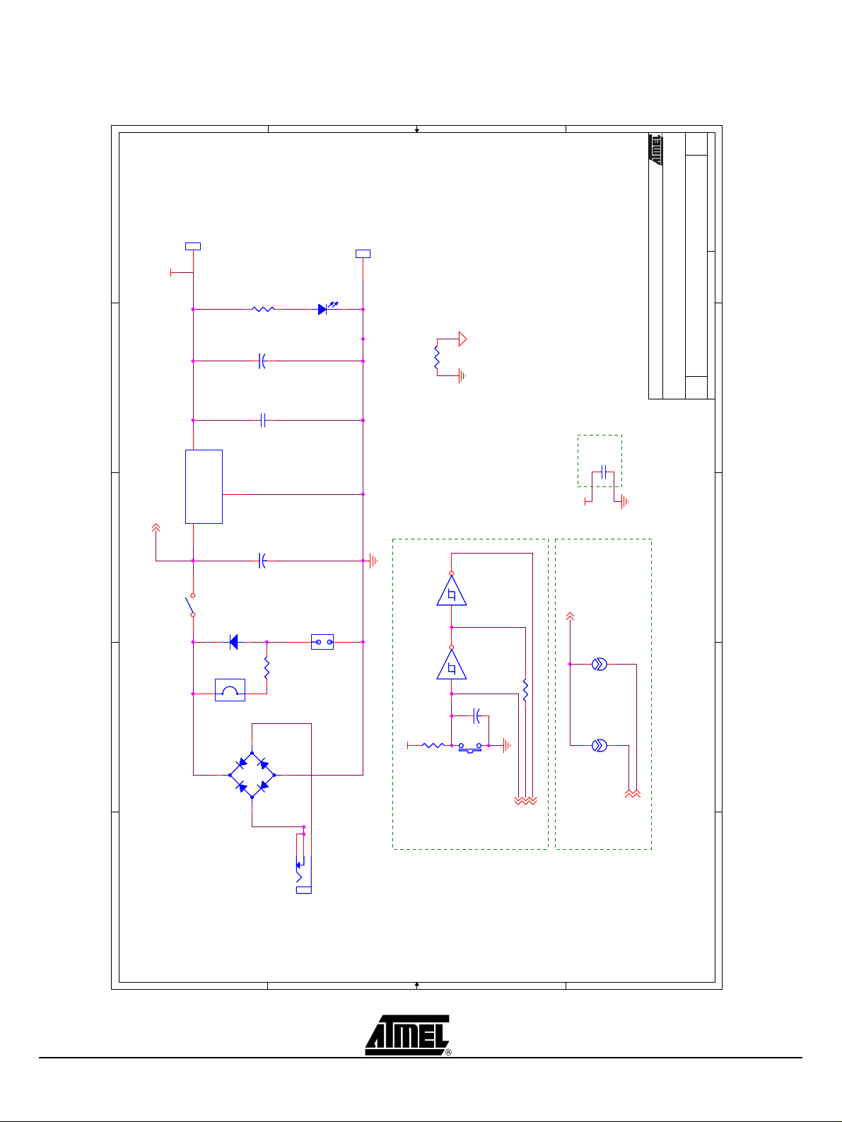
Figure 4-6. AT89STK-06 Board Schematics (4 of 4)
1
TP4
VCC
TP4
VCC
1
VCC
R17
1.2 K
R17
1.2 K
C30
4.7 µF
C30
4.7 µF
2
C29
100 nF
C29
100 nF
2
VOUT
GND
3
VIN
U9
MC78M05CDT
U9
MC78M05CDT
VPOWER
1
D8
LED PWR RED
PWRD8LED PWR RED
PWR
TP5
TP5
of
44Monday, May 24, 2004
44Monday, May 24, 2004
44Monday, May 24, 2004
1
GND
GND
1
AGND
R200R20
0
C32
C32
100 nF
100 nF
CD74HC14D
VCC
<Doc> 1.0.0
CC0x_demob/POWER
<Doc> 1.0.0
CC0x_demob/POWER
<Doc> 1.0.0
CC0x_demob/POWER
A4
A4
A4
Title
Size Document Number Rev
Title
Size Document Number Rev
Title
Size Document Number Rev
2
Date: Sheet
Date: Sheet of
Date: Sheet of
3
ON/OFF
SW1
SW1
1 2
JP6
JP6
4
5
SWITCH SSL
SWITCH SSL
D7
MRA4007D7MRA4007
Batt
Batt
+
U8
DF005S
U8
DF005S
3
C28
4.7 µF
C28
4.7 µF
1 2
R16
100
R16
100
1 2
-
2
-+
-+
1
J4
4
321
Charge
J5
BatteryJ5Battery
1 2
Batt- Batt+
CONNECTOR JACK PWR
PowerJ4CONNECTOR JACK PWR
Power
R18
10 k
R18
10 k
Vcc
Reset Circuit
U10B
U10B
U10A
U10A
74HC14D
74HC14D
3 4
74HC14D
74HC14D
R19
C31
C31
1 µF
1 µF
SW5
SW5
R19
PUSHBUTTON
PUSHBUTTON
/RST_UART
RST
1 2
RESET
RESET
/RST
1 K
1 K
XTAL2
SP3SP3
X2_44 X2_52
SP2SP2
Clock Circuit
"Solder Strap"
"Solder Strap"
XTAL2_44
XTAL2_52
3
4
5
D D
C C
B B
A A
4-18 AT89STK-06 Demo Board Software Demo Guide
4339C–CAN–07/05
Page 20

Appendix D: Default Configuration
Appendix D: Default Configuration
Table 1. Default Configuration
Reference Name Function State
SP1 CC02 mode
SP2 X2_44
For T89C51CC02/T89C5115 usage, allow to redirect the
ISP signal to P1.0, for hardware conditions.
Connect PLCC44 Xtal2 to XTAL2 of the generic extension
board
Open
Open
SP3 X2_52
JP1 EA
JP2 MUTE
JP3 CANRes
JP4 RTS
JP5 DTR
JP6 Batt
Connect PLCC52 Xtal2 to XTAL2 of the generic extension
board
ON : allows external execution
OFF: Internal code execution
ON : Enable C51 generic extension board buzzer
OFF: Disable C51 generic extension board buzzer
ON : Enable CAN terminator resistor
OFF: Disable CAN terminator resistor
ON : Enable RTS line to control ISP mode
OFF: Disable RTS line to control ISP mode
ON : Enable DTR line to drive MCU reset
OFF: Disable DTR line to drive MCU reset
ON : Enable Battery charge
OFF: Disable Battery charge
Open
Open (OFF)
Open (OFF)
Open (OFF)
Open (OFF)
Open (OFF)
Open (OFF)
AT89STK-06 Demo Board Software Demo Guide 4-19
4339C–CAN–07/05
Page 21

Appendix E: References/Acronyms
Appendix E: References/Acronyms
4.1 References AT89C51CC03, T89C51CC02, T89C51CC01, T89C5115, AT89C51AC3,
T89C51AC2 Product Datasheets*
4.2 Acronyms API: Application Programming Interface
FLIP: FLexible In-system Programming
HPC: High Pin Count microcontroller (by opposition to LPC)
ISP: In-System Programming
LPC: Low Pin Count microcontroller
4-20 AT89STK-06 Demo Board Software Demo Guide
4339C–CAN–07/05
Page 22

Atmel Headquarters Atmel Operatio ns
Corporate Headquarters
2325 Orchard Parkway
San Jose, CA 95131
TEL 1(408) 441-0311
FAX 1(408) 487-2600
Europe
Atmel Sarl
Route des Arsenaux 41
Case Postale 80
CH-1705 Fribourg
Switzerland
TEL (41) 26-426-5555
FAX (41) 26-426-5500
Asia
Room 1219
Chinachem Golden Plaza
77 Mody Road Tsimhatsui
East Kowloon
Hong Kong
TEL (852) 2721-9778
FAX (852) 2722-1369
Japan
9F, Tonetsu Shinkawa Bldg.
1-24-8 Shinkawa
Chuo-ku, Tokyo 104-0033
Japan
TEL (81) 3-3523-3551
FAX (81) 3-3523-7581
Memory
2325 Orchard Parkway
San Jose, CA 95131
TEL 1(408) 441-0311
FAX 1(408) 436-4314
Microcontrollers
2325 Orchard Parkway
San Jose, CA 95131
TEL 1(408) 441-0311
FAX 1(408) 436-4314
La Chantrerie
BP 70602
44306 Nantes Cedex 3, France
TEL (33) 2-40-18-18-18
FAX (33) 2-40-18-19-60
ASIC/ASSP/Smart Cards
Zone Industrielle
13106 Rousset Cedex, France
TEL (33) 4-42-53-60-00
FAX (33) 4-42-53-60-01
1150 East Cheyenne Mtn. Blvd.
Colorado Springs, CO 80906
TEL 1(719) 576-3300
FAX 1(719) 540-1759
Scottish Enterprise Technology Park
Maxwell Building
East Kilbride G75 0QR, Scotland
TEL (44) 1355-803-000
FAX (44) 1355-242-743
RF/Automotive
Theresienstrasse 2
Postfach 3535
74025 Heilbronn, Germany
TEL (49) 71-31-67-0
FAX (49) 71-31-67-2340
1150 East Cheyenne Mtn. Blvd.
Colorado Springs, CO 80906
TEL 1(719) 576-3300
FAX 1(719) 540-1759
Biometrics/Imaging/Hi-Rel MPU/
High Speed Converters/RF Datacom
Avenue de Rochepleine
BP 123
38521 Saint-Egreve Cedex, France
TEL (33) 4-76-58-30-00
FAX (33) 4-76-58-34-80
e-mail
literature@atmel.com
Web Site
http://www.atmel.com
Disclaimer: The information in this document is provided in connection with Atmel products. No license, express or implied, by estoppel or otherwise, to any
intellectual property right is gra nted by this document or in connection with the sale of Atmel products. EXCEPT AS SET FORTH IN ATMEL’S TERMS AND CONDI-
TIONS OF SALE LOCATED ON ATMEL’S WEB SITE, ATMEL ASSUMES NO LIABILITY WHATSOEVER AND DISCLAIMS ANY EXPRESS, IMPLIED OR STATUTORY
WARRANTY RELATING TO ITS PRODUCTS INCLUDING, BUT NOT LIMITED TO, THE IMPLIED WARRANTY OF MERCHANTABILITY, FITNESS FOR A PARTICULAR
PURPOSE, OR NON-INFRINGEMENT. IN NO EVENT SHALL ATMEL BE LIABLE FOR ANY DIRECT, INDIRECT, CONSEQUENTIAL, PUNITIVE, SPECIAL OR INCIDENTAL DAMAGES (INCLUDING, WITHOUT LIMITATION, DAMAGES FOR LOSS OF PROFITS, BUSINESS INTERRUPTION, OR LOSS OF INFORMATION) ARISING OUT
OF THE USE OR INABILITY TO USE THIS DOCUMENT, EVEN IF ATMEL HAS BEEN ADVISED OF THE POSSIBILITY OF SUCH DAMAGES. Atmel makes no
representations or warranties with respect to the a ccuracy or com p l etene ss o f the con tents of this documen t and reserves the right to make changes to specificat ions
and product descriptions at any time without notice. Atmel does not make any commitment to upd ate the information contained here in. Unless specifically p rovided
otherwise, Atmel products are not suitable for, and shall not be used in, automotive applications. Atmel’s products are not intended, authorized, or warranted for use
as components in applications intended to support or sustain life.
© Atmel Corporation 2005. All rights reserved. Atmel®, logo and combinations thereof, Everywhere You Are
and others, are registered trademarks or trademarks of Atmel Corporation or its subsidiaries. Other terms and
product names may be trademarks of others.
®
Printed on recycled paper.
4339C–CAN–07/05
/xM
 Loading...