


BDTIC www.bdtic.com/ATMEL
Features
•
Compatible with MCS®-51 Products
•
12K Bytes of In-System Programmable (ISP) Flash Program Memory
– SPI Serial Interface for Program Downloading
– Endurance: 10,000 Write/Erase Cycles
•
2K Bytes EEPROM Data Memory
– Endurance: 100,000 Write/Erase Cycles
•
64-byte User Signature Array
•
2.7V to 5.5V Operating Range
•
Fully Static Operation: 0 Hz to 24 MHz (in x1 and x2 Modes)
•
Three-level Program Memory Lock
•
256 x 8-bit Internal RAM
•
32 Programmable I/O Lines
•
Three 16-bit Timer/Counters
•
Nine Interrupt Sources
•
Enhanced UART Serial Port with Framing Error Detection and Automatic
Address Recognition
•
Enhanced SPI (Double Write/Read Buffered) Serial Interface
•
Low-power Idle and Power-down Modes
•
Interrupt Recovery from Power-down Mode
•
Programmable Watchdog Timer
•
Dual Data Pointer
•
Power-off Flag
•
Flexible ISP Programming (Byte and Page Modes)
– Page Mode: 64 Bytes/Page for Code Memory, 32 Bytes/Page for Data Memory
•
Four-level Enhanced Interrupt Controller
•
Programmable and Fuseable x2 Clock Option
•
Internal Power-on Reset
•
42-pin PDIP Package Option for Reduced EMC Emission
•
Green (Pb/Halide-free) Packaging Option
8-bit
Microcontroller
with 12K Bytes
Flash and 2K
Bytes EEPROM
AT89S8253
1. Description
The AT89S8253 is a low-power, high-performance CMOS 8-bit microcontroller with
12K bytes of In-System Programmable (ISP) Flash program memory and 2K bytes of
EEPROM data memory. The device is manufactured using Atmel’s high-density nonvolatile memory technology and is compatible with the industry-standard MCS-51
instruction set and pinout. The on-chip downloadable Flash allows the program memory to be reprogrammed in-system through an SPI serial interface or by a
conventional nonvolatile memory programmer. By combining a versatile 8-bit CPU
with downloadable Flash on a monolithic chip, the Atmel AT89S8253 is a powerful
microcontroller which provides a highly-flexible and cost-effective solution to many
embedded control applications.
3286K–MICRO–12/06
The AT89S8253 provides the following standard features: 12K bytes of In-System Programmable Flash, 2K bytes of EEPROM, 256 bytes of RAM, 32 I/O lines, programmable watchdog timer,
two data pointers, three 16-bit timer/counters, a six-vector, four-level interrupt architecture, a full
duplex serial port, on-chip oscillator, and clock circuitry. In addition, the AT89S8253 is designed
with static logic for operation down to zero frequency and supports two software selectable
power saving modes. The Idle Mode stops the CPU while allowing the RAM, timer/counters,
serial port, and interrupt system to continue functioning. The Power-down mode saves the RAM
contents but freezes the oscillator, disabling all other chip functions until the next external interrupt or hardware reset.
The on-board Flash/EEPROM is accessible through the SPI serial interface. Holding RESET
active forces the SPI bus into a serial programming interface and allows the program memory to
be written to or read from, unless one or more lock bits have been activated.
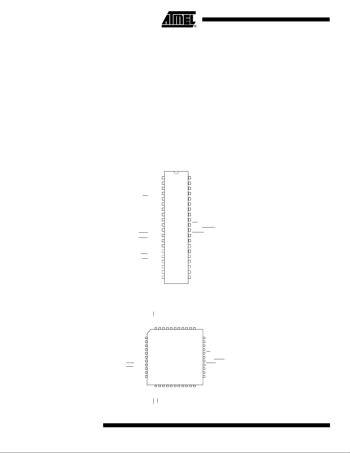
2. Pin Configurations
2.1 40P6 – 40-lead PDIP
2.2 44A – 44-lead TQFP
(T2 EX) P1.1
(MOSI) P1.5
(MISO) P1.6
(SCK) P1.7
(RXD) P3.0
(TXD) P3.1
(INT0) P3.2
(INT1) P3.3
(WR) P3.6
(MOSI) P1.5
(MISO) P1.6
(SCK) P1.7
RST
(RXD) P3.0
NC
(TXD) P3.1
(INT0) P3.2
(INT1) P3.3
(T0) P3.4
(T1) P3.5
(T2) P1.0
P1.2
P1.3
(SS) P1.4
RST
(T0) P3.4
(T1) P3.5
(RD) P3.7
XTAL2
XTAL1
GND
P1.4 (SS)
P1.3
4443424140393837363534
1
2
3
4
5
6
7
8
9
10
11
1213141516171819202122
1
2
3
4
5
6
7
8
9
10
11
12
13
14
15
16
17
18
19
20
P1.2
P1.1 (T2 EX)
P1.0 (T2)NCVCC
40
VCC
39
P0.0 (AD0)
38
P0.1 (AD1)
37
P0.2 (AD2)
36
P0.3 (AD3)
35
P0.4 (AD4)
34
P0.5 (AD5)
33
P0.6 (AD6)
32
P0.7 (AD7)
31
EA/VPP
30
ALE/PROG
29
PSEN
28
P2.7 (A15)
27
P2.6 (A14)
26
P2.5 (A13)
25
P2.4 (A12)
24
P2.3 (A11)
23
P2.2 (A10)
22
P2.1 (A9)
21
P2.0 (A8)
P0.0 (AD0)
P0.1 (AD1)
P0.2 (AD2)
P0.3 (AD3)
33
P0.4 (AD4)
32
P0.5 (AD5)
31
P0.6 (AD6)
30
P0.7 (AD7)
29
EA/VPP
28
NC
27
ALE/PROG
26
PSEN
25
P2.7 (A15)
24
P2.6 (A14)
23
P2.5 (A13)
GND
GND
XTAL2
XTAL1
(A8) P2.0
(RD) P3.7
(WR) P3.6
2
AT89S8253
(A9) P2.1
(A10) P2.2
(A11) P2.3
(A12) P2.4
3286K–MICRO–12/06
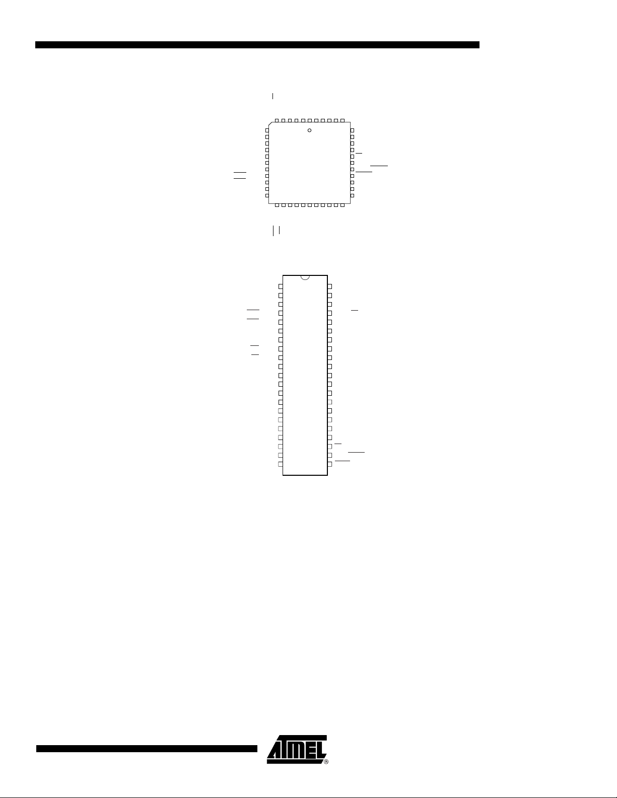
2.3 44J – 44-lead PLCC
2.4 42PS6 – PDIP
(MOSI) P1.5
(MISO) P1.6
(SCK) P1.7
RST
(RXD) P3.0
NC
(TXD) P3.1
(INT0) P3.2
(INT1) P3.3
(T0) P3.4
(T1) P3.5
P1.4 (SS)
P1.3
P1.2
P1.1 (T2 EX)
P1.0 (T2)NCVCC
GND
XTAL1
P0.0 (AD0)
1
4443424140
NC
(A8) P2.0
(A9) P2.1
65432
7
8
9
10
11
12
13
14
15
16
17
1819202122232425262728
XTAL2
(RD) P3.7
(WR) P3.6
P0.1 (AD1)
P0.2 (AD2)
P0.3 (AD3)
39
38
37
36
35
34
33
32
31
30
29
(A10) P2.2
(A11) P2.3
(A12) P2.4
P0.4 (AD4)
P0.5 (AD5)
P0.6 (AD6)
P0.7 (AD7)
EA/VPP
NC
ALE/PROG
PSEN
P2.7 (A15)
P2.6 (A14)
P2.5 (A13)
AT89S8253
3. Pin Description
3.1 VCC
Supply voltage (all packages except 42-PDIP).
RST
(RXD) P3.0
(TXD) P3.1
(INT0) P3.2
(INT1) P3.3
(T0) P3.4
(T1) P3.5
(WR) P3.6
(RD) P3.7
XTAL2
XTAL1
GND
PWRGND
(A8) P2.0
(A9) P2.1
(A10) P2.2
(A11) P2.3
(A12) P2.4
(A13) P2.5
(A14) P2.6
(A15) P2.7
1
2
3
4
5
6
7
8
9
10
11
12
13
14
15
16
17
18
19
20
21
42
41
40
39
38
37
36
35
34
33
32
31
30
29
28
27
26
25
24
23
22
P1.7 (SCK)
P1.6 (MISO)
P1.5 (MOSI)
P1.4 (SS)
P1.3
P1.2
P1.1 (T2EX)
P1.0 (T2)
VDD
PWRVDD
P0.0 (AD0)
P0.1 (AD1)
P0.2 (AD2)
P0.3 (AD3)
P0.4 (AD4)
P0.5 (AD5)
P0.6 (AD6)
P0.7 (AD7)
EA/VPP
ALE/PROG
PSEN
3.2 GND
3.3 VDD
3.4 PWRVDD
3286K–MICRO–12/06
Ground (all packages except 42-PDIP; for 42-PDIP GND connects only the logic core and the
embedded program/data memories).
Supply voltage for the 42-PDIP which connects only the logic core and the embedded program/data memories.
Supply voltage for the 42-PDIP which connects only the I/O Pad Drivers.
The application board must connect both VDD and PWRVDD to the board supply voltage.
3

3.5 PWRGND
3.6 Port 0
3.7 Port 1
Ground for the 42-PDIP which connects only the I/O Pad Drivers. PWRGND and GND are
weakly connected through the common silicon substrate, but not through any metal links. The
application board must connect both GND and PWRGND to the board ground.
Port 0 is an 8-bit open drain bi-directional I/O port. As an output port, each pin can sink six TTL
inputs. When 1s are written to port 0 pins, the pins can be used as high-impedance inputs.
Port 0 can also be configured to be the multiplexed low-order address/data bus during accesses
to external program and data memory. In this mode, P0 has internal pull-ups.
Port 0 also receives the code bytes during Flash programming and outputs the code bytes during program verification. External pull-ups are required during program verification.
Port 1 is an 8-bit bi-directional I/O port with internal pull-ups. The Port 1 output buffers can
sink/source six TTL inputs. When 1s are written to Port 1 pins, they are pulled high by the weak
internal pull-ups and can be used as inputs. As inputs, Port 1 pins that are externally being
pulled low will source current (I
,150 µA typical) because of the weak internal pull-ups.
IL
Some Port 1 pins provide additional functions. P1.0 and P1.1 can be configured to be the
timer/counter 2 external count input (P1.0/T2) and the timer/counter 2 trigger input (P1.1/T2EX),
respectively.
3.8 Port 2
Furthermore, P1.4, P1.5, P1.6, and P1.7 can be configured as the SPI slave port select, data
input/output and shift clock input/output pins as shown in the following table.
Port Pin Alternate Functions
P1.0 T2 (external count input to Timer/Counter 2), clock-out
P1.1 T2EX (Timer/Counter 2 capture/reload trigger and direction control)
P1.4 SS
P1.5 MOSI (Master data output, slave data input pin for SPI channel)
P1.6 MISO (Master data input, slave data output pin for SPI channel)
P1.7 SCK (Master clock output, slave clock input pin for SPI channel)
(Slave port select input)
Port 1 also receives the low-order address bytes during Flash programming and verification.
Port 2 is an 8-bit bi-directional I/O port with internal pull-ups. The Port 2 output buffers can
sink/source six TTL inputs. When 1s are written to Port 2 pins, they are pulled high by the weak
internal pull-ups and can be used as inputs. As inputs, Port 2 pins that are externally being
pulled low will source current (I
,150 µA typical) because of the weak internal pull-ups.
IL
Port 2 emits the high-order address byte during fetches from external program memory and during accesses to external data memory that use 16-bit addresses (MOVX @ DPTR). In this
application, Port 2 uses strong internal pull-ups when emitting 1s. During accesses to external
data memory that use 8-bit addresses (MOVX @ RI), Port 2 emits the contents of the P2
Special Function Register.
Port 2 also receives the high-order address bits and some control signals during Flash
programming and verification.
4
AT89S8253
3286K–MICRO–12/06

3.9 Port 3
AT89S8253
Port 3 is an 8-bit bi-directional I/O port with internal pull-ups. The Port 3 output buffers can
sink/source six TTL inputs. When 1s are written to Port 3 pins, they are pulled high by the weak
internal pull-ups and can be used as inputs. As inputs, Port 3 pins that are externally being
pulled low will source current (I
Port 3 receives some control signals for Flash programming and verification.
Port 3 also serves the functions of various special features of the AT89S8253, as shown in the
following table.
Port Pin Alternate Functions
P3.0 RXD (serial input port)
P3.1 TXD (serial output port)
P3.2 INT0
P3.3 INT1 (external interrupt 1)
P3.4 T0 (timer 0 external input)
P3.5 T1 (timer 1 external input)
P3.6 WR
P3.7 RD
Note: 1. All pins in ports 1 and 2 and almost all pins in port 3 (the exceptions are P3.2 INT0 and P3.3
INT1) have their inputs disabled in the Power-down mode. Port pins P3.2 (INT0) and P3.3
(INT1
the Power-down mode) and as such still have their weak internal pull-ups turned on.
(external interrupt 0)
(external data memory write strobe)
(external data memory read strobe)
) are active even in Power-down mode (to be able to sense an interrupt request to exit
,150 µA typical) because of the weak internal pull-ups.
IL
(1)
(1)
3.10 RST
3.11 ALE/PROG
3.12 PSEN
Reset input. A high on this pin for at least two machine cycles while the oscillator is running
resets the device.
Address Latch Enable. ALE/PROG is an output pulse for latching the low byte of the address (on
its falling edge) during accesses to external memory. This pin is also the program pulse input
(PROG
) during Flash programming.
In normal operation, ALE is emitted at a constant rate of 1/6 the oscillator frequency and may be
used for external timing or clocking purposes. Note, however, that one ALE pulse is skipped during each access to external data memory.
If desired, ALE operation can be disabled by setting bit 0 of the AUXR SFR at location 8EH. With
the bit set, ALE is active only during a MOVX or MOVC instruction. Otherwise, the pin is weakly
pulled high. Setting the ALE-disable bit has no effect if the microcontroller is in external execution mode.
Program Store Enable. PSEN is the read strobe to external program memory (active low).
When the AT89S8253 is executing code from external program memory, PSEN
twice each machine cycle, except that two PSEN
activations are skipped during each access to
is activated
external data memory.
3286K–MICRO–12/06
5
3.13 EA/VPP
3.14 XTAL1
3.15 XTAL2
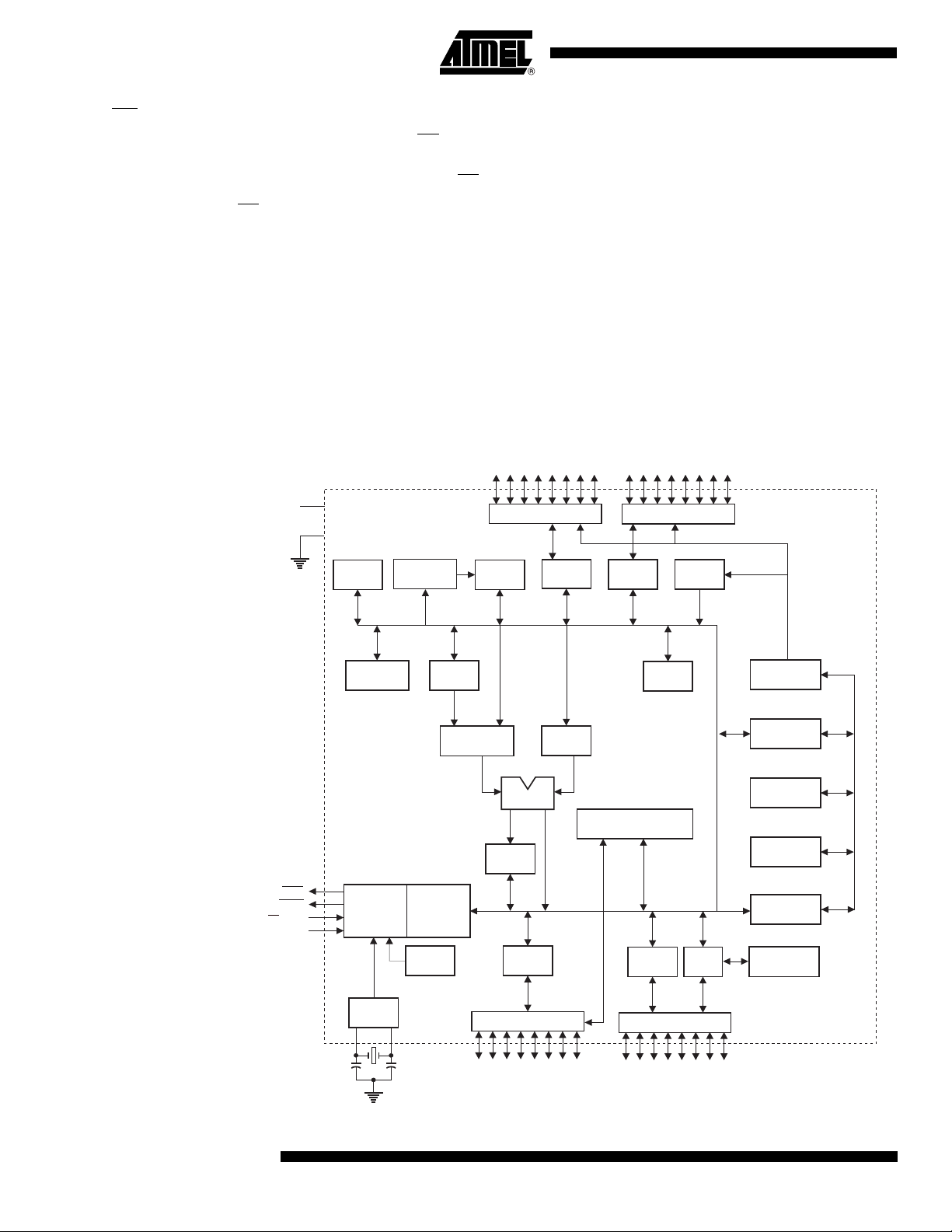
4. Block Diagram
External Access Enable. EA must be strapped to GND in order to enable the device to fetch
code from external program memory locations starting at 0000H up to FFFFH. Note, however,
that if lock bit 1 is programmed, EA
EA
should be strapped to VCC for internal program executions. This pin also receives the 12-volt
programming enable voltage (V
will be internally latched on reset.
) during Flash programming when 12-volt programming is
PP
selected.
Input to the inverting oscillator amplifier and input to the internal clock operating circuit.
Output from the inverting oscillator amplifier.
PSEN
ALE/PROG
EA / V
RST
V
GND
PP
PORT 2 DRIVERS
PORT 2
LATCH
PORT 1
LATCH
P2.0 - P2.7
STACK
POINTER
FLASH
SPI
PORT
PROGRAM
ADDRESS
REGISTER
BUFFER
PC
INCREMENTER
PROGRAM
COUNTER
DUAL
DPTR
PROGRAM
LOGIC
P0.0 - P0.7
CC
TIMING
AND
B
RAM ADDR.
REGISTER
INSTRUCTION
REGISTER
WATCH
DOG
ACC
EEPROM
REGISTER
CONTROL
PORT 0 DRIVERS
ALU
PORT 3
LATCH
PORT 0
LATCH
RAM
TMP2 TMP1
PSW
INTERRUPT, SERIAL PORT,
AND TIMER BLOCKS
OSC
6
AT89S8253
PORT 3 DRIVERS
P3.0 - P3.7
PORT 1 DRIVERS
P1.0 - P1.7
3286K–MICRO–12/06

AT89S8253
5. Special Function Registers
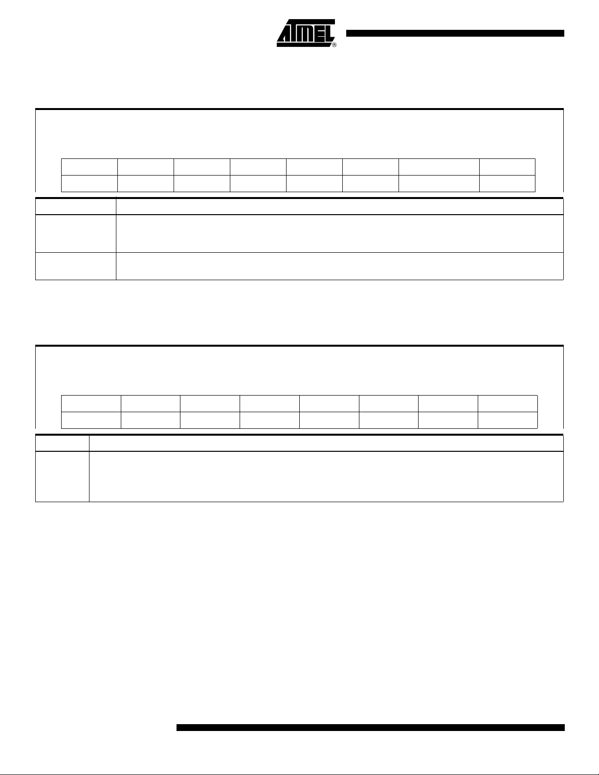
A map of the on-chip memory area called the Special Function Register (SFR) space is shown in
Table 5-1.
Note that not all of the addresses are occupied, and unoccupied addresses may not be implemented on the chip. Read accesses to these addresses will generally return random data, and
write accesses will have an indeterminate effect.
User software should not write 1s to these unlisted locations, since they may be used in future
products to invoke new features. In that case, the reset or inactive values of the new bits will
always be 0.
Table 5-1. AT89S8253 SFR Map and Reset Values
0F8H 0FFH
0F0H
0E8H 0EFH
0E0H
0D8H 0DFH
0D0H
0C8H
0C0H 0C7H
0B8H
0B0H
0A8H
0A0H
98H
90H
88H
80H
B
00000000
ACC
00000000
PSW
00000000
T2CON
00000000
IP
XX000000
P3
11111111
IE
0X000000
P2
11111111
SCON
00000000
P1
11111111
TCON
00000000
P0
11111111
T2MOD
XXXXXX00
SADEN
00000000
SADDR
00000000
SBUF
XXXXXXXX
TMOD
00000000
SP
00000111
RCAP2L
00000000
SPSR
000XXX00
TL0
00000000
DP0L
00000000
RCAP2H
00000000
TL1
00000000
DP0H
00000000
TL2
00000000
TH0
00000000
DP1L
00000000
SPCR
00000100
TH2
00000000
TH1
00000000
DP1H
00000000
WDTRST
(Write Only)
EECON
XX000011
AUXR
XXXXXXX0
SPDR
########
IPH
XX000000
WDTCON
0000 0000
CLKREG
XXXXXXX0
PCON
00XX0000
Note: # means: 0 after cold reset and unchanged after warm reset.
0F7H
0E7H
0D7H
0CFH
0BFH
0B7H
0AFH
0A7H
9FH
97H
8FH
87H
3286K–MICRO–12/06
7
5.1 Auxiliary Register
The AUXR Register contains a single active bit called DISALE.
Table 5-2. AUXR – Auxiliary Register
AUXR Address = 8EH Reset Value = XXXX XXX0B
Not Bit Addressable
––––––Intel_Pwd_ExitDISALE
Bit765432 1 0
Symbol Function
When set, this bit configures the interrupt driven exit from power-down to resume execution on the rising edge of
Intel_Pwd_Exit
DISALE
the interrupt signal. When this bit is cleared, the execution resumes after a self-timed interval (nominal 2 ms)
referenced from the falling edge of the interrupt signal.
When DISALE = 0, ALE is emitted at a constant rate of 1/6 the oscillator frequency (except during MOVX when 1
ALE pulse is missing). When DISALE = 1, ALE is active only during a MOVX or MOVC instruction.
5.2 Clock Register
The CLKREG register contains a single active bit called X2.
Table 5-3. CLKREG – Clock Register
CLKREG Address = 8FH Reset Value = XXXX XXX0B
Not Bit Addressable
–––––––X2
Bit76543210
Symbol Function
When X2 = 0, the oscillator frequency (at XTAL1 pin) is internally divided by 2 before it is used as the device system
X2
frequency.
When X2 = 1, the divider by 2 is no longer used and the XTAL1 frequency becomes the device system frequency. This
enables the user to choose a 6 MHz crystal instead of a 12 MHz crystal, for example, in order to reduce EMI.
5.3 SPI Registers
Control and status bits for the Serial Peripheral Interface are contained in registers SPCR (see
Table 14-1 on page 25) and SPSR (see Table 14-2 on page 26). The SPI data bits are contained
in the SPDR register. In normal SPI mode, writing the SPI data register during serial data transfer sets the Write Collision bit (WCOL) in the SPSR register. In enhanced SPI mode, the SPDR
is also write double-buffered because WCOL works as a Write Buffer Full Flag instead of being a
collision flag. The values in SPDR are not changed by Reset.
5.4 Interrupt Registers
The global interrupt enable bit and the individual interrupt enable bits are in the IE register. In
addition, the individual interrupt enable bit for the SPI is in the SPCR register. Four priorities can
be set for each of the six interrupt sources in the IP and IPH registers.
IPH bits have the same functions as IP bits, except IPH has higher priority than IP. By using IPH
in conjunction with IP, a priority level of 0, 1, 2, or 3 may be set for each interrupt.
8
AT89S8253
3286K–MICRO–12/06

5.5 Dual Data Pointer Registers
To facilitate accessing both internal EEPROM and external data memory, two banks of 16-bit
Data Pointer Registers are provided: DP0 at SFR address locations 82H - 83H and DP1 at 84H
- 85H. Bit DPS = 0 in SFR EECON selects DP0 and DPS = 1 selects DP1. The user should
ALWAYS initialize the DPS bit to the appropriate value before accessing the respective Data
Pointer Register.
5.6 Power Off Flag
The Power Off Flag (POF), located at bit_4 (PCON.4) in the PCON SFR. POF, is set to “1” during power up. It can be set and reset under software control and is not affected by RESET.
6. Data Memory – EEPROM and RAM
The AT89S8253 implements 2K bytes of on-chip EEPROM for data storage and 256 bytes of
RAM. The upper 128 bytes of RAM occupy a parallel space to the Special Function Registers.
That means the upper 128 bytes have the same addresses as the SFR space but are physically
separate from SFR space.
When an instruction accesses an internal location above address 7FH, the address mode used
in the instruction specifies whether the CPU accesses the upper 128 bytes of RAM or the SFR
space. Instructions that use direct addressing access the SFR space.
AT89S8253
For example, the following direct addressing instruction accesses the SFR at location 0A0H
(which is P2).
MOV 0A0H, #data
Instructions that use indirect addressing access the upper 128 bytes of RAM. For example, the
following indirect addressing instruction, where R0 contains 0A0H, accesses the data byte at
address 0A0H, rather than P2 (whose address is 0A0H).
MOV @R0, #data
Note that stack operations are examples of indirect addressing, so the upper 128 bytes of data
RAM are available as stack space.
The on-chip EEPROM data memory is selected by setting the EEMEN bit in the EECON register
at SFR address location 96H. The EEPROM address range is from 000H to 7FFH. MOVX
instructions are used to access the EEPROM. To access off-chip data memory with the MOVX
instructions, the EEMEN bit needs to be set to “0”.
During program execution mode (using the MOVX instruction) there is an auto-erase capability
at the byte level. This means that the user can update or modify a single EEPROM byte location
in real-time without affecting any other bytes.
The EEMWE bit in the EECON register needs to be set to “1” before any byte location in the
EEPROM can be written. User software should reset EEMWE bit to “0” if no further EEPROM
write is required. EEPROM write cycles in the serial programming mode are self-timed and typically take 4 ms. The progress of EEPROM write can be monitored by reading the RDY/BSY
(read-only) in SFR EECON. RDY/BSY
= 1 means an EEPROM write cycle is completed and another write cycle can be initiated. Bit
EELD in EECON controls whether the next MOVX instruction will only load the write buffer of the
EEPROM or will actually start the programming cycle. By setting EELD, only load will occur.
Before the last MOVX in a given page of 32 bytes, EELD should be cleared so that after the last
MOVX the entire page will be programmed at the same time. This way, 32 bytes will only require
4 ms of programming time instead of 128 ms required in single byte programming.
= 0 means programming is still in progress and RDY/BSY
bit
3286K–MICRO–12/06
9
In addition, during EEPROM programming, an attempted read from the EEPROM will fetch the
byte being written with the MSB complemented. Once the write cycle is completed, true data are
valid at all bit locations.
6.1 Memory Control Register
The EECON register contains control bits for the 2K bytes of on-chip data EEPROM. It also contains the control bit for the dual data pointer.
Table 6-1. EECON – Data EEPROM Control Register
EECON Address = 96H Reset Value = XX00 0011B
Not Bit Addressable
Bit – – EELD EEMWE EEMEN DPS RDY/BSY
765432 1 0
Symbol Function
EEPROM data memory load enable bit. Used to implement Page Mode Write. A MOVX instruction writing into the data
EELD
EEMWE
EEMEN
DPS
RDY/BSY
WRTINH
EEPROM will not initiate the programming cycle if this bit is set, rather it will just load data into the volatile data buffer of
the data EEPROM memory. Before the last MOVX, reset this bit and the data EEPROM will program all the bytes
previously loaded on the same page of the address given by the last MOVX instruction.
EEPROM data memory write enable bit. Set this bit to 1 before initiating byte write to on-chip EEPROM with the MOVX
instruction. User software should set this bit to 0 after EEPROM write is completed.
Internal EEPROM access enable. When EEMEN = 1, the MOVX instruction with DPTR will access on-chip EEPROM
instead of external data memory if the address used is less than 2K. When EEMEN = 0 or the address used is ≥ 2K,
MOVX with DPTR accesses external data memory.
Data pointer register select. DPS = 0 selects the first bank of data pointer register, DP0, and DPS = 1 selects the
second bank, DP1.
RDY/BSY (Ready/Busy) flag for the data EEPROM memory. This is a read-only bit which is cleared by hardware during
the programming cycle of the on-chip EEPROM. It is also set by hardware when the programming is completed. Note
that RDY/BSY
cycle.
WRTINH (Write Inhibit) is a READ-ONLY bit which is cleared by hardware when Vcc is too low for the programming cycle
of the on-chip EEPROM to be executed. When this bit is cleared, an ongoing programming cycle will be aborted or a
new programming cycle will not start.
will be cleared long after the completion of the MOVX instruction which has initiated the programming
WRTINH
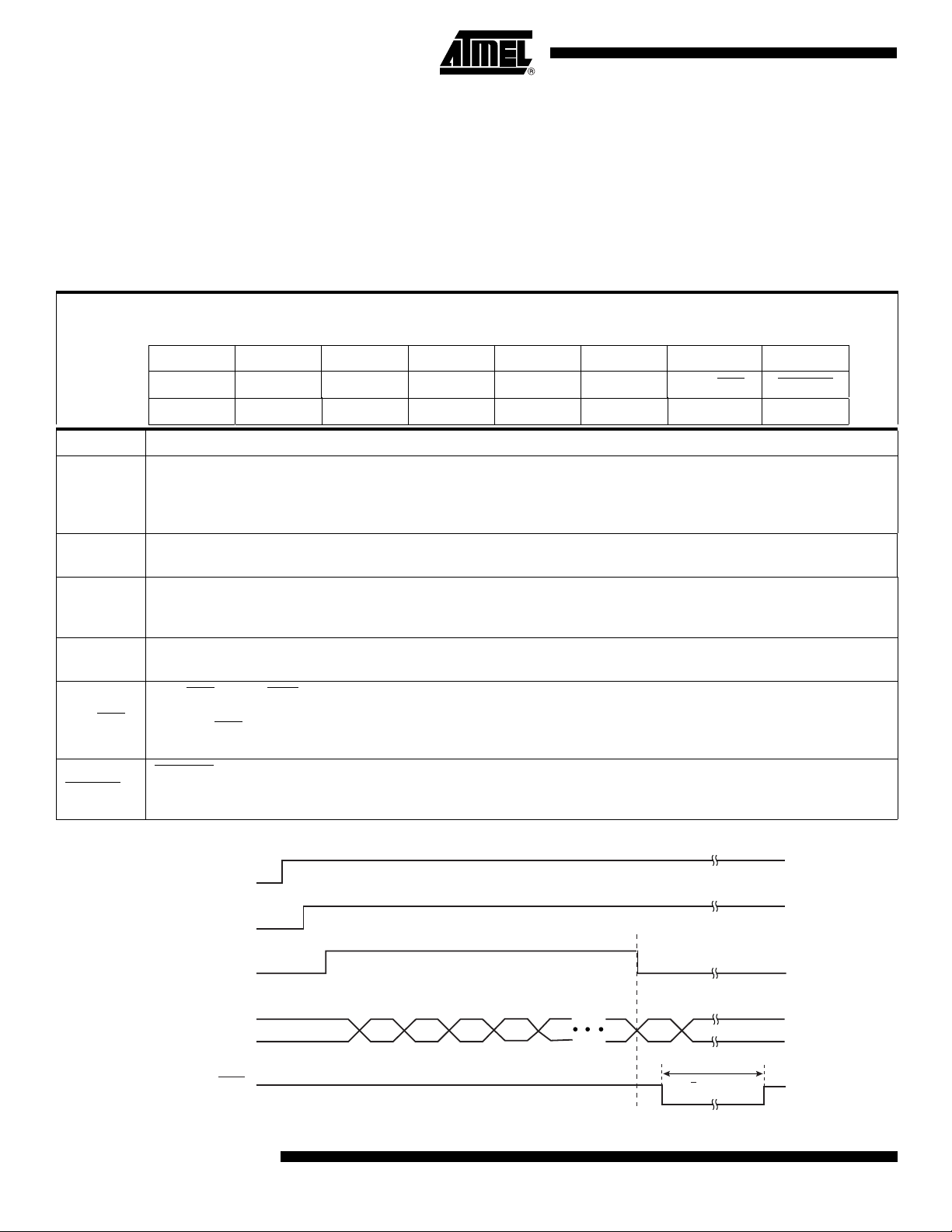
Figure 6-1. Data EEPROM Write Sequence
EEMEN
EEMWE
EELD
MOVX DATA
RDY/BSY
10
AT89S8253
0 1 2 3 30 31
~
4 ms
3286K–MICRO–12/06
7. Power-On Reset
A Power-On Reset (POR) is generated by an on-chip detection circuit. The detection level is
nominally 1.4V. The POR is activated whenever V
cuit can be used to trigger the start-up reset or to detect a supply voltage failure in devices
without a brown-out detector. The POR circuit ensures that the device is reset from power-on.
When V
how long the device is kept in POR after V
again, without any delay, when V
a cold reset) will set the POF flag in PCON.
Figure 7-1. Power-up and Brown-out Detection Sequence
V
CC
Level 2.7V
Min V
CC
BOD Level 2.3V
POR Level 1.4V
POR
reaches the Power-on Reset threshold voltage, the POR delay counter determines
CC
AT89S8253
is below the detection level. The POR cir-
CC
rise, nominally 2 ms. The POR signal is activated
CC
falls below the POR threshold level. A Power-On Reset (i.e.
CC
t
XTAL1
BOD
Internal
RESET
0
7.1 Brown-out Reset
The AT89S8253 has an on-chip Brown-out Detection (BOD) circuit for monitoring the VCC level
during operation by comparing it to a fixed trigger level of 2.4V (max). The trigger level for the
BOD is nominally 2.2V. The purpose of the BOD is to ensure that if V
cuting at speed, the system will gracefully enter reset without the possibility of errors induced by
incorrect execution. When V
is immediately activated. When V
starts the MCU after the timeout period has expired in approximately 2 ms.
t
POR
(2 ms)
2.4V
t
1.2V
t
t
t
POR
(2 ms)
t
fails or dips while exe-
CC
decreases to a value below the trigger level, the Brown-out Reset
CC
increases above the trigger level, the BOD delay counter
CC
3286K–MICRO–12/06
11

8. Programmable Watchdog Timer
The programmable Watchdog Timer (WDT) counts instruction cycles. The prescaler bits, PS0,
PS1 and PS2 in SFR WDTCON are used to set the period of the Watchdog Timer from 16K to
2048K instruction cycles. The available timer periods are shown in Table 8-1.
period is dependent upon the external clock frequency.
The WDT is disabled by Power-on Reset and during Power-down mode. When WDT times out
without being serviced or disabled, an internal RST pulse is generated to reset the CPU. See
Table 8-1 for the WDT period selections.
Table 8-1. Watchdog Timer Time-out Period Selection
The WDT time-out
WDT Prescaler Bits
0 0 0 16 ms
0 0 1 32 ms
0 1 0 64 ms
011 128 ms
100 256 ms
101 512 ms
1 1 0 1024 ms
1 1 1 2048 ms
Period (Nominal for
= 12 MHz)PS2 PS1 PS0
F
CLK
12
AT89S8253
3286K–MICRO–12/06
AT89S8253
8.1 Watchdog Control Register
The WDTCON register contains control bits for the Watchdog Timer (shown in Table 8-2).
Table 8-2. WDTCON – Watchdog Control Register
WDTCON Address = A7H Reset Value = 0000 0000B
Not Bit Addressable
PS2 PS1 PS0 WDIDLE DISRTO HWDT WSWRST WDTEN
Bit76543210
Symbol Function
PS2
PS1
PS0
Prescaler bits for the watchdog timer (WDT). When all three bits are cleared to 0, the watchdog timer has a nominal
period of 16K machine cycles, (i.e. 16 ms at a XTAL frequency of 12 MHz in normal mode or 6 MHz in x2 mode). When
all three bits are set to 1, the nominal period is 2048K machine cycles, (i.e. 2048 ms at 12 MHz clock frequency in
normal mode or 6 MHz in x2 mode).
WDIDLE
DISRTO
HWDT
WSWRST
WDTEN
Enable/disable the Watchdog Timer in IDLE mode. When WDIDLE = 0, WDT continues to count in IDLE mode. When
WDIDLE = 1, WDT freezes while the device is in IDLE mode.
Enable/disable the WDT-driven Reset Out (WDT drives the RST pin). When DISRTO = 0, the RST pin is driven high
after WDT times out and the entire board is reset. When DISRTO = 1, the RST pin remains only as an input and the
WDT resets only the microcontroller internally after WDT times out.
Hardware mode select for the WDT. When HWDT = 0, the WDT can be turned on/off by simply setting or clearing
WDTEN in the same register (this is the software mode for WDT). When HWDT = 1, the WDT has to be set by writing
the sequence 1EH/E1H to the WDTRST register (with address 0A6H) and after being set in this way, WDT cannot be
turned off except by reset, warm or cold (this is the hardware mode for WDT). To prevent the hardware WDT from
resetting the entire device, the same sequence 1EH/E1H must be written to the same WDTRST SFR before the
timeout interval.
Watchdog software reset bit. If HWDT = 0 (i.e. WDT is in software controlled mode), when set by software, this bit resets
WDT. After being set by software, WSWRST is reset by hardware during the next machine cycle. If HWDT = 1, this bit
has no effect, and if set by software, it will not be cleared by hardware.
Watchdog software enable bit. When HWDT = 0 (i.e. WDT is in software-controlled mode), this bit enables WDT when
set to 1 and disables WDT when cleared to 0 (it does not reset WDT in this case, but just freezes the existing counter
state). If HWDT = 1, this bit is READ-ONLY and reflects the status of the WDT (whether it is running or not).
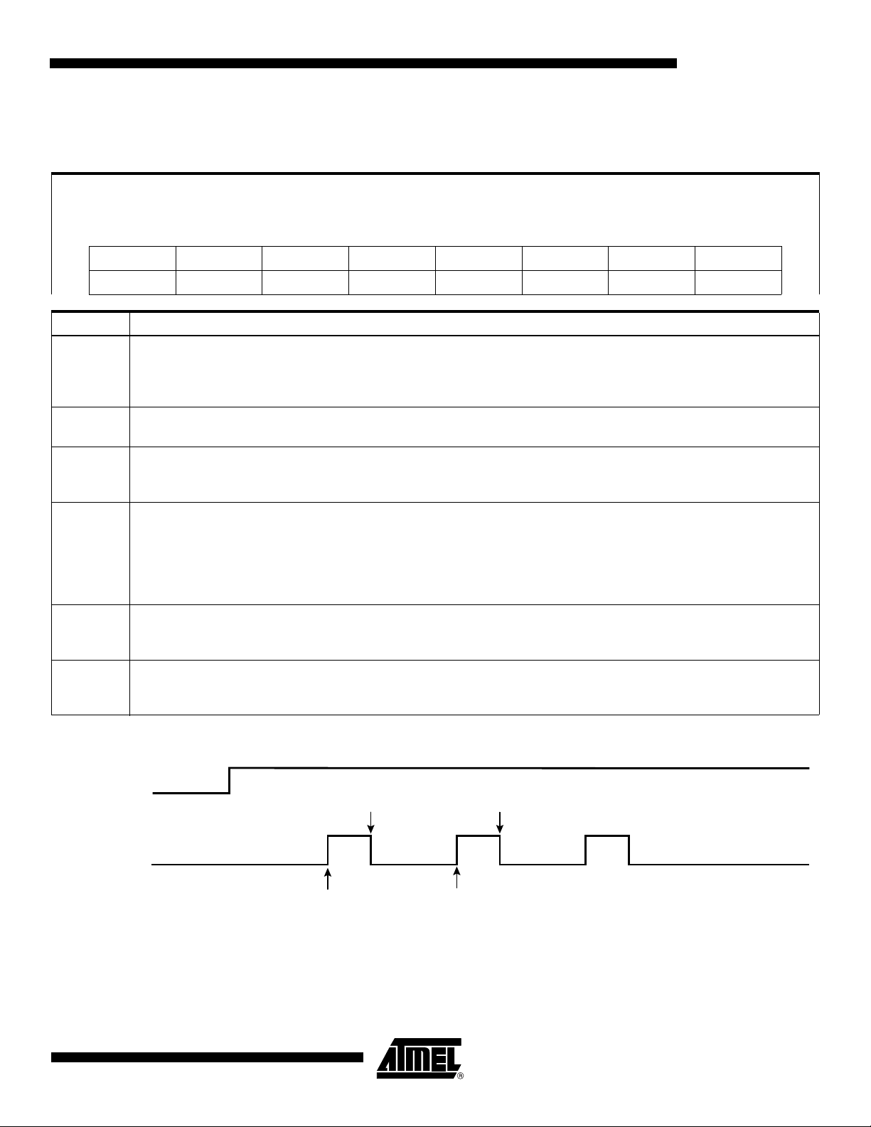
Figure 8-1. Software Mode – Watchdog Timer Sequence
WDTEN
HWHW
WSWRST
3286K–MICRO–12/06
SW Writes a 1
SW
13
9. Timer 0 and 1
10. Timer 2
Timer 0 and Timer 1 in the AT89S8253 operate the same way as Timer 0 and Timer 1 in the
AT89S51 and AT89S52. For more detailed information on the Timer/Counter operation, please
click on the document link below:
http://www.atmel.com/dyn/resources/prod_documents/DOC4316.PDF
Timer 2 is a 16-bit Timer/Counter that can operate as either a timer or an event counter. The
type of operation is selected by bit C/T2
2 has three operating modes: capture, auto-reload (up or down counting), and baud rate generator. The modes are selected by bits in T2CON, as shown in Table 10-2.
Timer 2 consists of two 8-bit registers, TH2 and TL2. In the Timer function, the TL2 register is
incremented every machine cycle. Since a machine cycle consists of 12 oscillator periods, the
count rate is 1/12 of the oscillator frequency.
In the Counter function, the register is incremented in response to a 1-to-0 transition at its corresponding external input pin, T2. In this function, the external input is sampled during S5P2 of
every machine cycle. When the samples show a high in one cycle and a low in the next cycle,
the count is incremented. The new count value appears in the register during S3P1 of the cycle
following the one in which the transition was detected. Since two machine cycles (24 oscillator
periods) are required to recognize a 1-to-0 transition, the maximum count rate is 1/24 of the
oscillator frequency. To ensure that a given level is sampled at least once before it changes, the
level should be held for at least one full machine cycle.
in the SFR T2CON (see Table 10-2 on page 15). Timer
Table 10-1. Timer 2 Operating Modes
RCLK + TCLK CP/RL2 TR2 MODE
0 0 1 16-bit Auto-reload
0 1 1 16-bit Capture
1 X 1 Baud Rate Generator
XX0(Off)
14
AT89S8253
3286K–MICRO–12/06
AT89S8253
Table 10-2. T2CON – Timer/Counter 2 Control Register
T2CON Address = 0C8H Reset Value = 0000 0000B
Bit Addressable
TF2 EXF2 RCLK TCLK EXEN2 TR2 C/T2 CP/RL2
Bit76543210
Symbol Function
TF2
EXF2
RCLK
TCLK
EXEN2
TR2 Start/Stop control for Timer 2. TR2 = 1 starts the timer.
C/T2
CP/RL2
Timer 2 overflow flag set by a Timer 2 overflow and must be cleared by software. TF2 will not be set when either
RCLK = 1 or TCLK = 1.
Timer 2 external flag set when either a capture or reload is caused by a negative transition on T2EX and EXEN2 = 1.
When Timer 2 interrupt is enabled, EXF2 = 1 will cause the CPU to vector to the Timer 2 interrupt routine. EXF2 must be
cleared by software. EXF2 does not cause an interrupt in up/down counter mode (DCEN = 1).
Receive clock enable. When set, causes the serial port to use Timer 2 overflow pulses for its receive clock in serial port
Modes 1 and 3. RCLK = 0 causes Timer 1 overflows to be used for the receive clock.
Transmit clock enable. When set, causes the serial port to use Timer 2 overflow pulses for its transmit clock in serial port
Modes 1 and 3. TCLK = 0 causes Timer 1 overflows to be used for the transmit clock.
Timer 2 external enable. When set, allows a capture or reload to occur as a result of a negative transition on T2EX if
Timer 2 is not being used to clock the serial port. EXEN2 = 0 causes Timer 2 to ignore events at T2EX.
Timer or counter select for Timer 2. C/T2 = 0 for timer function. C/T2 = 1 for external event counter (falling edge
triggered).
Capture/Reload select. CP/RL2 = 1 causes captures to occur on negative transitions at T2EX if EXEN2 = 1. CP/RL2 = 0
causes automatic reloads to occur when Timer 2 overflows or negative transitions occur at T2EX when EXEN2 = 1. When
either RCLK or TCLK = 1, this bit is ignored and the timer is forced to auto-reload on Timer 2 overflow.
10.1 Timer 2 Registers
Control and status bits are contained in registers T2CON (see Table 10-2) and T2MOD (see
Table 10-3) for Timer 2. The register pair (RCAP2H, RCAP2L) are the Capture/Reload registers
for Timer 2 in 16-bit capture mode or 16-bit auto-reload mode.
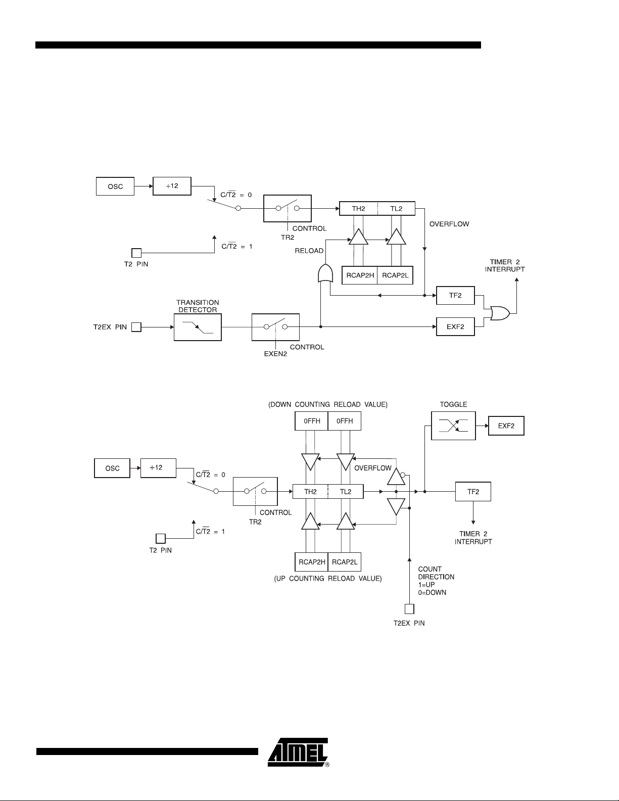
10.2 Capture Mode
3286K–MICRO–12/06
In the capture mode, two options are selected by bit EXEN2 in T2CON. If EXEN2 = 0, Timer 2 is
a 16-bit timer or counter which upon overflow sets bit TF2 in T2CON. This bit can then be used
to generate an interrupt. If EXEN2 = 1, Timer 2 performs the same operation, but a 1-to-0 transition at external input T2EX also causes the current value in TH2 and TL2 to be captured into
RCAP2H and RCAP2L, respectively. In addition, the transition at T2EX causes bit EXF2 in
T2CON to be set. The EXF2 bit, like TF2, can generate an interrupt. The capture mode is illustrated in Figure 10-1.
15
Figure 10-1. Timer 2 in Capture Mode
OSC
T2 PIN
T2EX PIN
÷12
C/T2 = 0
C/T2 = 1
TRANSITION
DETECTOR
EXEN2
10.3 Auto-reload (Up or Down Counter)
Timer 2 can be programmed to count up or down when configured in its 16-bit auto-reload
mode. This feature is invoked by the DCEN (Down Counter Enable) bit located in the SFR
T2MOD (see Table 10-3). Upon reset, the DCEN bit is set to 0 so that timer 2 will default to
count up. When DCEN is set, Timer 2 can count up or down, depending on the value of the
T2EX pin.
CONTROL
TR2
CAPTURE
CONTROL
TH2 TL2
RCAP2LRCAP2H
EXF2
TF2
OVERFLOW
TIMER 2
INTERRUPT
Table 10-3. T2MOD – Timer 2 Mode Control Register
T2MOD Address = 0C9H Reset Value = XXXX XX00B
Not Bit Addressable
––––––T2OEDCEN
Bit76543210
Symbol Function
– Not implemented, reserved for future use.
T2OE Timer 2 Output Enable bit.
DCEN When set, this bit allows Timer 2 to be configured as an up/down counter.
Figure 10-2 shows Timer 2 automatically counting up when DCEN = 0. In this mode, two options
are selected by bit EXEN2 in T2CON. If EXEN2 = 0, Timer 2 counts up to 0FFFFH and then sets
the TF2 bit upon overflow. The overflow also causes the timer registers to be reloaded with the
16-bit value in RCAP2H and RCAP2L. The values in RCAP2H and RCAP2L are preset by software. If EXEN2 = 1, a 16-bit reload can be triggered either by an overflow or by a 1-to-0
transition at external input T2EX. This transition also sets the EXF2 bit. Both the TF2 and EXF2
bits can generate an interrupt if enabled.
Setting the DCEN bit enables Timer 2 to count up or down, as shown in Figure 10-3. In this
mode, the T2EX pin controls the direction of the count. A logic 1 at T2EX makes Timer 2 count
up. The timer will overflow at 0FFFFH and set the TF2 bit. This overflow also causes the 16-bit
value in RCAP2H and RCAP2L to be reloaded into the timer registers, TH2 and TL2,
respectively.
16
AT89S8253
3286K–MICRO–12/06
A logic 0 at T2EX makes Timer 2 count down. The timer underflows when TH2 and TL2 equal
the values stored in RCAP2H and RCAP2L. The underflow sets the TF2 bit and causes 0FFFFH
to be reloaded into the timer registers.
The EXF2 bit toggles whenever Timer 2 overflows or underflows and can be used as a 17th bit
of resolution. In this operating mode, EXF2 does not flag an interrupt.
Figure 10-2. Timer 2 in Auto Reload Mode (DCEN = 0)
AT89S8253
Figure 10-3. Timer 2 Auto Reload Mode (DCEN = 1 Timer 2 Auto Reload Mode (DCEN = 1)
3286K–MICRO–12/06
17
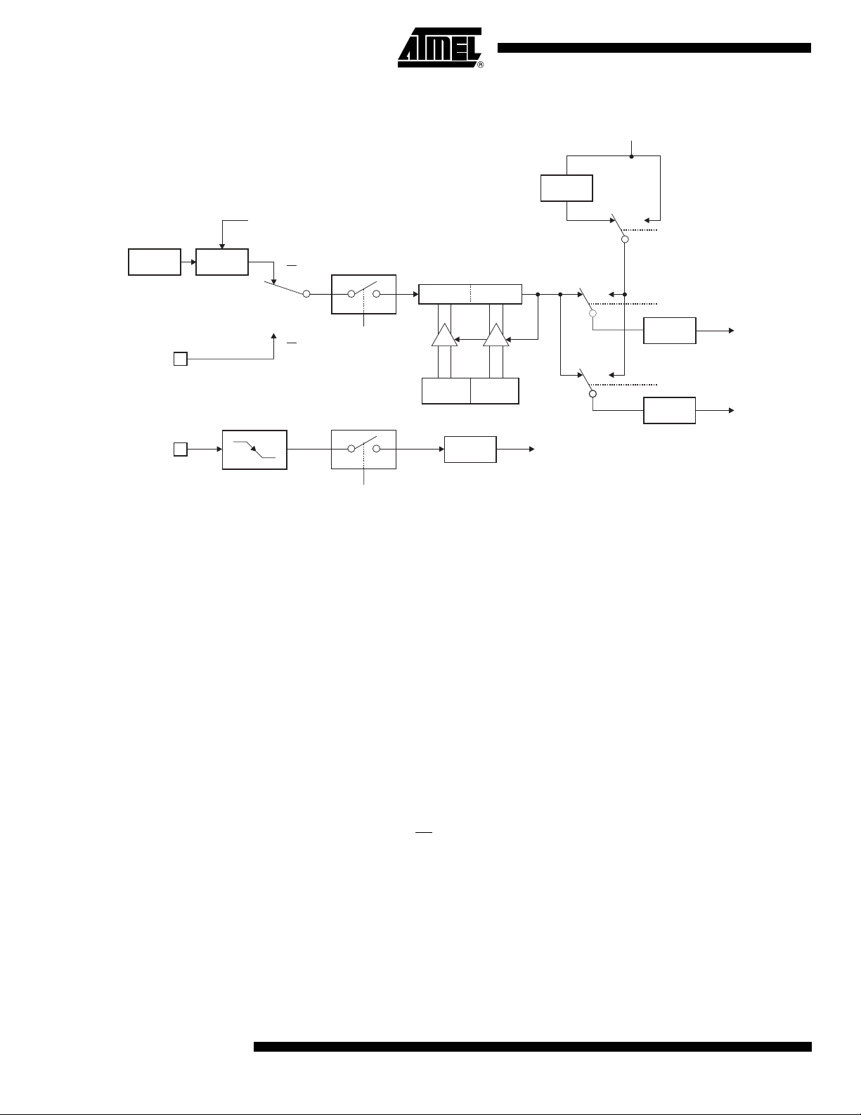
Figure 10-4. Timer 2 in Baud Rate Generator Mode
NOTE: OSC. FREQ. IS DIVIDED BY 2, NOT 12
TIMER 1 OVERFLOW
2
÷
"0"
"1"
SMOD1
OSC
T2 PIN
T2EX PIN
2
÷
TRANSITION
DETECTOR
11. Baud Rate Generator
Timer 2 is selected as the baud rate generator by setting TCLK and/or RCLK in T2CON (Table
10-2). Note that the baud rates for transmit and receive can be different if Timer 2 is used for the
receiver or transmitter and Timer 1 is used for the other function. Setting RCLK and/or TCLK
puts Timer 2 into its baud rate generator mode, as shown in Figure 10-4.
The baud rate generator mode is similar to the auto-reload mode, in that a rollover in TH2
causes the Timer 2 registers to be reloaded with the 16-bit value in registers RCAP2H and
RCAP2L, which are preset by software.
C/T2 = 0
C/T2 = 1
TR2
EXEN2
CONTROL
CONTROL
TH2 TL2
RCAP2LRCAP2H
EXF2
"1"
"1"
TIMER 2
INTERRUPT
"0"
"0"
RCLK
16
÷
TCLK
16
÷
Rx
CLOCK
Tx
CLOCK
18
The baud rates in Modes 1 and 3 are determined by Timer 2’s overflow rate according to the following equation.
The Timer can be configured for either timer or counter operation. In most applications, it is configured for timer operation (CP/T2
used as a baud rate generator. Normally, as a timer, it increments every machine cycle (at 1/12
the oscillator frequency). As a baud rate generator, however, it increments every state time (at
1/2 the oscillator frequency). The baud rate formula is given below.
where (RCAP2H, RCAP2L) is the content of RCAP2H and RCAP2L taken as a 16-bit unsigned
integer.
AT89S8253
Modes 1 and 3 Baud Rates
= 0). The timer operation is different for Timer 2 when it is
Modes 1 and 3
-------------------------------------- -
Baud Rate
-----------------------------------------------------------------------------------------------=
32 65536 RCAP2H,RCAP2L()–[]×
Timer 2 Overflow Rate
----------------------------------------------------------- -=
16
Oscillator Frequency
3286K–MICRO–12/06

Timer 2 as a baud rate generator is shown in Figure 10-4. This figure is valid only if RCLK or
TCLK = 1 in T2CON. Note that a rollover in TH2 does not set TF2 and will not generate an interrupt. Note too, that if EXEN2 is set, a 1-to-0 transition in T2EX will set EXF2 but will not cause a
reload from (RCAP2H, RCAP2L) to (TH2, TL2). Thus when Timer 2 is in use as a baud rate generator, T2EX can be used as an extra external interrupt.
Note that when Timer 2 is running (TR2 = 1) as a timer in the baud rate generator mode, TH2 or
TL2 should not be read from or written to. Under these conditions, the Timer is incremented
every state time, and the results of a read or write may not be accurate. The RCAP2 registers
may be read but should not be written to, because a write might overlap a reload and cause
write and/or reload errors. The timer should be turned off (clear TR2) before accessing the Timer
2 or RCAP2 registers.
12. Programmable Clock Out
A 50% duty cycle clock can be programmed to come out on P1.0, as shown in Figure 12-1. This
pin, besides being a regular I/O pin, has two alternate functions. It can be programmed to input
the external clock for Timer/Counter 2 or to output a 50% duty cycle clock ranging from 61 Hz to
4 MHz (for a 16 MHz operating frequency).
AT89S8253
To configure the Timer/Counter 2 as a clock generator, bit C/T2
bit T2OE (T2MOD.1) must be set. Bit TR2 (T2CON.2) starts and stops the timer.
The clock-out frequency depends on the oscillator frequency and the reload value of Timer 2
capture registers (RCAP2H, RCAP2L), as shown in the following equation.
In the clock-out mode, Timer 2 rollovers will not generate an interrupt. This behavior is similar to
when Timer 2 is used as a baud-rate generator. It is possible to use Timer 2 as a baud-rate generator and a clock generator simultaneously. Note, however, that the baud-rate and clock-out
frequencies cannot be determined independently from one another since they both use
RCAP2H and RCAP2L.
Figure 12-1. Timer 2 in Clock-out Mode
Clock Out Frequency
Oscillator Frequency
------------------------------------------------------------------------------------------- -=
4 65536 RCAP2H,RCAP2L()–[]×
(T2CON.1) must be cleared and
3286K–MICRO–12/06
19

13. UART
The UART in the AT89S8253 operates the same way as the UART in the AT89S51 and
AT89S52. For more detailed information on the UART operation, please click on the document
link below:
http://www.atmel.com/dyn/resources/prod_documents/DOC4316.PDF
13.1 Enhanced UART
In addition to all of its usual modes, the UART can perform framing error detection by looking for
missing stop bits, and automatic address recognition. The UART also fully supports multiprocessor communication as does the standard 80C51 UART.
When used for framing error detect, the UART looks for missing stop bits in the communication.
A missing bit will set the FE bit in the SCON register. The FE bit shares the SCON.7 bit with SM0
and the function of SCON.7 is determined by PCON.6 (SMOD0). If SMOD0 is set then SCON.7
functions as FE. SCON.7 functions as SM0 when SMOD0 is cleared. When used as FE,
SCON.7 can only be cleared by software.
13.1.1 Automatic Address Recognition
Automatic Address Recognition is a feature which allows the UART to recognize certain
addresses in the serial bit stream by using hardware to make the comparisons. This feature
saves a great deal of software overhead by eliminating the need for the software to examine
every serial address which passes by the serial port. This feature is enabled by setting the SM2
bit in SCON. In the 9-bit UART modes, mode 2 and mode 3, the Receive Interrupt flag (RI) will
be automatically set when the received byte contains either the “Given” address or the
“Broadcast” address. The 9-bit mode requires that the 9th information bit is a 1 to indicate that
the received information is an address and not data.
The 8-bit mode is called mode 1. In this mode the RI flag will be set if SM2 is enabled and the
information received has a valid stop bit following the 8 address bits and the information is either
a Given or Broadcast address.
Mode 0 is the Shift Register mode and SM2 is ignored.
Using the Automatic Address Recognition feature allows a master to selectively communicate
with one or more slaves by invoking the given slave address or addresses. All of the slaves may
be contacted by using the Broadcast address. Two special Function Registers are used to
define the slave’s address, SADDR, and the address mask, SADEN. SADEN is used to define
which bits in the SADDR are to be used and which bits are “don’t care”. The SADEN mask can
be logically ANDed with the SADDR to create the “Given” address which the master will use for
addressing each of the slaves. Use of the Given address allows multiple slaves to be recognized
while excluding others. The following examples will help to show the versatility of this scheme:
Slave 0 SADDR = 1100 0000
SADEN = 1111 1101
Given = 1100 00X0
Slave 1 SADDR = 1100 0000
SADEN = 1111 1110
Given = 1100 000X
20
AT89S8253
3286K–MICRO–12/06

AT89S8253
In the previous example SADDR is the same and the SADEN data is used to differentiate
between the two slaves. Slave 0 requires a 0 in bit 0 and it ignores bit 1. Slave 1 requires a 0 in
bit 1 and bit 0 is ignored. A unique address for slave 0 would be 1100 0010 since slave 1
requires a 0 in bit 1. A unique address for slave 1 would be 1100 0001 since a 1 in bit 0 will
exclude slave 0. Both slaves can be selected at the same time by an address which has bit 0 = 0
(for slave 0) and bit 1 = 0 (for slave 1). Thus, both could be addressed with 1100 0000.
In a more complex system the following could be used to select slaves 1 and 2 while excluding
slave 0:
Slave 0 SADDR = 1100 0000
SADEN = 1111 1001
Given = 1100 0XX0
Slave 1 SADDR = 1110 0000
SADEN = 1111 1010
Given = 1110 0X0X
Slave 2 SADDR = 1110 0000
SADEN = 1111 1100
Given = 1110 00XX
In the previous example the differentiation among the 3 slaves is in the lower 3 address bits.
Slave 0 requires that bit 0 = 0 and it can be uniquely addressed by 1110 0110. Slave 1 requires
that bit 1 = 0 and it can be uniquely addressed by 1110 and 0101. Slave 2 requires that bit 2 = 0
and its unique address is 1110 0011. To select Slaves 0 and 1 and exclude Slave 2, use
address 1110 0100, since it is necessary to make bit 2 = 1 to exclude slave 2.
The Broadcast Address for each slave is created by taking the logical OR of SADDR and
SADEN. Zeros in this result are trended as don’t-cares. In most cases, interpreting the don’tcares as ones, the broadcast address will be FF hexadecimal.
Upon reset SADDR (SFR address 0A9H) and SADEN (SFR address 0B9H) are loaded with 0s.
This produces a given address of all “don’t cares” as well as a Broadcast address of all “don’t
cares”. This effectively disables the Automatic Addressing mode and allows the microcontroller
to use standard 80C51-type UART drivers which do not make use of this feature.
3286K–MICRO–12/06
21

Table 13-1. PCON – Power Control Register
PCON Address = 87H Reset Value = 00xx 0000B
Bit Addressable
SMOD1 SMOD0 – POF GF1 GF0 PD IDL
Bit7 6543210
Symbol Function
SMOD1 Double Baud Rate bit. Doubles the baud rate of the UART in Modes 1, 2, or 3.
SMOD0 Frame Error Select. When SMOD0 = 1, SCON.7 is SM0. When SMOD0 = 1, SCON.7 is FE. Note that FE will be set after
a frame error regardless of the state of SMOD0.
POF Power Off Flag. POF is set to “1” during power up (i.e. cold reset). It can be set or reset under software control and is not
affected by RST or BOD (i.e. warm resets).
GF1, GF0 General-purpose Flags
PD Power-down bit. Setting this bit activates power-down operation.
IDL Idle Mode bit. Setting this bit activates Idle mode operation
Table 13-2. SCON – Serial Port Control Register
SCON Address = 98H Reset Value = 0000 0000B
Bit Addressable
SM0/FE SM1 SM2 REN TB8 RB8 T1 RI
Bit7 6543210
(SMOD0 = 0/1)
(1)
Symbol Function
Framing error bit. This bit is set by the receiver when an invalid stop bit is detected. The FE bit is not cleared by valid
FE
frames but should be cleared by software. The SMOD0 bit must be set to enable access to the FE bit. FE will be set
regardless of the state of SMOD0.
SM0 Serial Port Mode Bit 0, (SMOD0 must = 0 to access bit SM0)
Serial Port Mode Bit 1
SM1
SM0 SM1 Mode Description Baud Rate
0 0 0 shift register f
0 1 1 8-bit UART variable
1 0 2 9-bit UART f
osc
/64 or f
osc
/12
osc
(2)
/32
1 1 3 9-bit UART variable
Enables the Automatic Address Recognition feature in modes 2 or 3. If SM2 = 1 then Rl will not be set unless the received
SM2
9th data bit (RB8) is 1, indicating an address, and the received byte is a Given or Broadcast Address. In mode 1, if SM2 =
1 then Rl will not be activated unless a valid stop bit was received, and the received byte is a Given or Broadcast Address.
In Mode 0, SM2 should be 0.
REN Enables serial reception. Set by software to enable reception. Clear by software to disable reception.
TB8 The 9th data bit that will be transmitted in modes 2 and 3. Set or clear by software as desired.
RB8
TI
RI
In modes 2 and 3, the 9th data bit that was received. In mode 1, if SM2 = 0, RB8 is the stop bit that was received. In mode
0, RB8 is not used.
Transmit interrupt flag. Set by hardware at the end of the 8th bit time in mode 0, or at the beginning of the stop bit in the
other modes, in any serial transmission. Must be cleared by software.
Receive interrupt flag. Set by hardware at the end of the 8th bit time in mode 0, or halfway through the stop bit time in the
other modes, in any serial reception (except see SM2). Must be cleared by software.
Notes: 1. SMOD0 is located at PCON.6.
2. f
= oscillator frequency.
osc
22
AT89S8253
3286K–MICRO–12/06

14. Serial Peripheral Interface
The serial peripheral interface (SPI) allows high-speed synchronous data transfer between the
AT89S8253 and peripheral devices or between multiple AT89S8253 devices. The AT89S8253
SPI features include the following:
• Full-Duplex, 3-Wire Synchronous Data Transfer
• Master or Slave Operation
• Maximum Bit Frequency = f/4 (f/2 if in x2 Clock Mode)
• LSB First or MSB First Data Transfer
• Four Programmable Bit Rates in Master Mode
• End of Transmission Interrupt Flag
• Write Collision Flag Protection
• Double-Buffered Receive
• Double-Buffered Transmit (Enhanced Mode only)
• Wakeup from Idle Mode (Slave Mode only)
The interconnection between master and slave CPUs with SPI is shown in Figure 14-1. The four
pins in the interface are Master-In/Slave-Out (MISO), Master-Out/Slave-In (MOSI), Shift Clock
(SCK), and Slave Select (SS
input in slave mode. The MSTR bit in SPCR determines the directions of MISO and MOSI. Also
notice that MOSI connects to MOSI and MISO to MISO. In master mode, SS
may be used as a general-purpose input or output. In slave mode, SS
select an individual device as a slave. When SS
vated and the MOSI/P1.5 pin can be used as a general-purpose input.
AT89S8253
). The SCK pin is the clock output in master mode, but is the clock
/P1.4 is ignored and
must be driven low to
is driven high, the slave’s SPI port is deacti-
Figure 14-1. SPI Master-Slave Interconnection
MSB LSB
8-BIT SHIFT REGISTER
SPI
CLOCK GENERATOR
MASTER
MISO
MISO
MOSI MOSI
SCK
SS SS
SCK
V
CC
MSB LSB
8-BIT SHIFT REGISTER
SLAVE
3286K–MICRO–12/06
23

Figure 14-2. SPI Block Diagram
OSCILLATOR
DIVIDER
÷4÷16÷64÷128
MSB
8-BIT SHIFT REGISTER
READ DATA BUFFER
WRITE DATA BUFFER
LSB
S
M
M
S
(1)
MISO
MOSI
OL LOGIC
P1.6
P1.5
DORD
CLOCK
LOGIC
MSTR
CLOCK
CPOL
CPHA
SPR1
SPR0
S
M
MSTR
PIN CONTR
SPE
DORD
SCK
P1.4
1.7
SS
SELECT
SPR1
SPI CONTROL
WCOL
SPIF
SPI STATU S REGISTER
SPI CLOCK (MASTER)
SPR0
SPI INTERRUPT
REQUEST
MSTR
SPE
8
8
INTERNAL
DATA BU S
SPIE
SPE
SPI CONTROL REGISTER
8
Note: 1. The Write Data Buffer is only used in enhanced SPI mode.
The SPI has two modes of operation: normal (non-buffered write) and enhanced (buffered
write). In normal mode, writing to the SPI data register (SPDR) of the master CPU starts the SPI
clock generator and the data written shifts out of the MOSI pin and into the MOSI pin of the slave
CPU. Transmission may start after an initial delay while the clock generator waits for the next full
bit slot of the specified baud rate. After shifting one byte, the SPI clock generator stops, setting
the end of transmission flag (SPIF) and transferring the received byte to the read buffer (SPDR).
If both the SPI interrupt enable bit (SPIE) and the serial port interrupt enable bit (ES) are set, an
interrupt is requested. Note that SPDR refers to either the write data buffer or the read data
buffer, depending on whether the access is a write or read. In normal mode, because the write
buffer is transparent (and a write access to SPDR will be directed to the shift buffer), any attempt
to write to SPDR while a transmission is in progress will result in a write collision with WCOL set.
However, the transmission will still complete normally, but the new byte will be ignored and a
new write access to SPDR will be necessary.
24
Enhanced mode is similar to normal mode except that the write buffer holds the next byte to be
transmitted. Writing to SPDR loads the write buffer and sets WCOL to signify that the buffer is
full and any further writes will overwrite the buffer. WCOL is cleared by hardware when the buffered byte is loaded into the shift register and transmission begins. If the master SPI is currently
idle, i.e. if this is the first byte, then after loading SPDR, transmission of the byte starts and
WCOL is cleared immediately. While this byte is transmitting, the next byte may be written to
SPDR. The Load Enable flag (LDEN) in SPSR can be used to determine when transmission has
started. LDEN is asserted during the first four bit slots of a SPI transfer. The master CPU should
first check that LDEN is set and that WCOL is cleared before loading the next byte. In enhanced
mode, if WCOL is set when a transfer completes, i.e. the next byte is available, then the SPI
immediately loads the buffered byte into the shift register, resets WCOL, and continues transmission without stopping and restarting the clock generator. As long as the CPU can keep the
write buffer full in this manner, multiple bytes may be transferred with minimal latency between
bytes.
AT89S8253
3286K–MICRO–12/06

AT89S8253
Table 14-1. SPCR – SPI Control Register
SPCR Address = D5H Reset Value = 0000 0100B
Not Bit Addressable
SPIE SPE DORD MSTR CPOL CPHA SPR1 SPR0
Bit76543210
Symbol Function
SPIE
SPE
DORD Data order. DORD = 1 selects LSB first data transmission. DORD = 0 selects MSB first data transmission.
MSTR Master/slave select. MSTR = 1 selects Master SPI mode. MSTR = 0 selects slave SPI mode.
CPOL
CPHA
SPR0
SPR1
Notes: 1. Set up the clock mode before enabling the SPI: set all bits needed in SPCR except the SPE bit, then set SPE.
SPI interrupt enable. This bit, in conjunction with the ES bit in the IE register, enables SPI interrupts: SPIE = 1 and ES = 1
enable SPI interrupts. SPIE = 0 disables SPI interrupts.
SPI enable. SPI = 1 enables the SPI channel and connects SS, MOSI, MISO and SCK to pins P1.4, P1.5, P1.6, and P1.7.
SPI = 0 disables the SPI channel.
Clock polarity. When CPOL = 1, SCK is high when idle. When CPOL = 0, SCK of the master device is low when not
transmitting. Please refer to figure on SPI clock phase and polarity control.
Clock phase. The CPHA bit together with the CPOL bit controls the clock and data relationship between master and slave.
Please refer to figure on SPI clock phase and polarity control.
SPI clock rate select. These two bits control the SCK rate of the device configured as master. SPR1 and SPR0 have no
effect on the slave. The relationship between SCK and the oscillator frequency, F
SPR1 SPR0 SCK
0 0 f/4 (f/2 in x2 mode)
0 1 f/16 (f/8 in x2 mode)
1 0 f/64 (f/32 in x2 mode)
1 1 f/128 (f/64 in x2 mode)
2. Enable the master SPI prior to the slave device.
3. Slave echoes master on next Tx if not loaded with new data.
, is as follows:
OSC.
3286K–MICRO–12/06
25

Table 14-2. SPSR – SPI Status Register
SPSR Address = AAH Reset Value = 000X XX00B
Not Bit Addressable
SPIF WCOL LDEN – – – DISSO ENH
Bit76543210
Symbol Function
SPIF
WCOL
LDEN
DISSO
ENH
SPI interrupt flag. When a serial transfer is complete, the SPIF bit is set and an interrupt is generated if SPIE = 1 and ES
= 1. The SPIF bit is cleared by reading the SPI status register followed by reading/writing the SPI data register.
When ENH = 0: Write collision flag. The WCOL bit is set if the SPI data register is written during a data transfer. During
data transfer, the result of reading the SPDR register may be incorrect, and writing to it has no effect. The WCOL bit (and
the SPIF bit) are cleared by reading the SPI status register followed by reading/writing the SPI data register.
When ENH = 1: WCOL works in Enhanced mode as Tx Buffer Full. Writing during WCOL = 1 in enhanced mode will
overwrite the waiting data already present in the Tx Buffer. In this mode, WCOL is no longer reset by the SPIF reset but
is reset when the write buffer has been unloaded into the serial shift register.
Load enable for the Tx buffer in enhanced SPI mode.
When ENH is set, it is safe to load the Tx Buffer while LDEN = 1 and WCOL = 0. LDEN is high during bits 0 - 3 and is low
during bits 4 - 7 of the SPI serial byte transmission time frame.
Disable slave output bit.
When set, this bit causes the MISO pin to be tri-stated so more than one slave device can share the same interface with
a single master. Normally, the first byte in a transmission could be the slave address and only the selected slave should
clear its DISSO bit.
Enhanced SPI mode select bit. When ENH = 0, SPI is in normal mode, i.e. without write double buffering.
When ENH = 1, SPI is in enhanced mode with write double buffering. The Tx buffer shares the same address with the
SPDR register.
Table 14-3. SPDR – SPI Data Register
SPDR Address = 86H
Not Bit Addressable
Reset Value = 00H (after cold reset)
unchanged (after warm reset)
SPD7 SPD6 SPD5 SPD4 SPD3 SPD2 SPD1 SPD0
Bit76543210
26
AT89S8253
3286K–MICRO–12/06

Figure 14-3. SPI Shift Register Diagram
AT89S8253
7
Serial In
Transmit
Byte
The CPHA (C
8
2:1
MUX
8 8
lock PHAse), CPOL (Clock POLarity), and SPR (Serial Peripheral clock Rate =
Serial Master Serial Slave
DQ
LATCH
CLK
8
Parallel Master
(Write Buffer)
DQ
LATCH
CLK
2:1
MUX
DQ
LATCH
CLK
Parallel Slave
(Read Buffer)
DQ
LATCH
CLK
Serial Out
Receive
Byte
8
baud rate) bits in SPCR control the shape and rate of SCK. The two SPR bits provide four possible clock rates when the SPI is in master mode. In slave mode, the SPI will operate at the rate of
the incoming SCK as long as it does not exceed the maximum bit rate. There are also four possible combinations of SCK phase and polarity with respect to the serial data. CPHA and CPOL
determine which format is used for transmission. The SPI data transfer formats are shown in
Figure 14-4 and Figure 14-5. To prevent glitches on SCK from disrupting the interface, CPHA,
CPOL, and SPR should be set up before the interface is enabled, and the master device should
be enabled before the slave device(s).
3286K–MICRO–12/06
Table 14-4. SPI Master Characteristics
Symbol Parameter Min Max Units
t
CLCL
t
SCK
t
SHSL
t
SLSH
t
SR
t
SF
t
SIS
t
SIH
t
SOH
t
SOV
Oscillator Period 41.6 ns
Serial Clock Cycle Time 4t
Clock High Time t
Clock Low Time t
CLCL
/2 - 25 ns
SCK
/2 - 25 ns
SCK
Rise Time 25 ns
Fall Time 25 ns
Serial Input Setup Time 10 ns
Serial Input Hold Time 10 ns
Serial Output Hold Time 10 ns
Serial Output Valid Time 35 ns
ns
27

Table 14-5. SPI Slave Characteristics
Symbol Parameter Min Max Units
t
CLCL
t
SCK
t
SHSL
t
SLSH
t
SR
t
SF
t
SIS
t
SIH
t
SOH
t
SOV
t
SOE
t
SOX
t
SSE
t
SSD
Oscillator Period 41.6 ns
Serial Clock Cycle Time 4t
Clock High Time 1.5 t
Clock Low Time 1.5 t
CLCL
- 25 ns
CLCL
- 25 ns
CLCL
Rise Time 25 ns
Fall Time 25 ns
Serial Input Setup Time 10 ns
Serial Input Hold Time 10 ns
Serial Output Hold Time 10 ns
Serial Output Valid Time 35 ns
Output Enable Time 10 ns
Output Disable Time 25 ns
Slave Enable Lead Time 10 ns
Slave Disable Lag Time 0 ns
Figure 14-4. SPI Master Timing (CPHA = 0)
ns
SS
SCK
(CPOL = 0)
SCK
(CPOL = 1)
MISO
MOSI
t
SHSL
t
SLSH
t
SCK
t
SR
t
SLSH
t
SHSL
t
SOH
t
SOV
t
SF
t
SIS
t
SIH
28
AT89S8253
3286K–MICRO–12/06

Figure 14-5. SPI Slave Timing (CPHA = 0)
SS
SCK
t
t
SLSH
SCK
t
SSE
t
SHSL
t
(CPOL = 0)
SCK
(CPOL= 1)
t
SOE
t
SLSH
t
SHSL
MISO
MOSI
Figure 14-6. SPI Master Timing (CPHA = 1)
SS
t
SCK
SCK
t
SHSL
t
SLSH
(CPOL = 0)
SR
t
SOV
AT89S8253
t
SIH
t
SSD
t
SOX
t
SF
t
SOH
t
SIS
t
SF
t
SR
SCK
(CPOL = 1)
t
SLSH
t
SHSL
MISO
MOSI
Figure 14-7. SPI Slave Timing (CPHA = 1)
SS
t
SCK
t
SLSH
SCK
t
SSE
t
SHSL
(CPOL = 0)
SCK
(CPOL = 1)
t
SOE
t
SLSH
t
SHSL
MISO
t
SIS
t
SIH
MOSI
t
SOH
t
SIS
t
SOV
t
SF
t
SOV
t
SOH
t
SIH
t
SR
t
SOX
t
SSD
3286K–MICRO–12/06
29

Figure 14-8. SPI Transfer Format with CPHA = 0
Note: *Not defined but normally MSB of character just received
Figure 14-9. SPI Transfer Format with CPHA = 1
SCK CYCLE #
(FOR REFERENCE)
SCK (CPOL = 0)
SCK (CPOL = 1)
1 2 3 4 5 6 7 8
(FROM MASTER)
MOSI
MISO
(FROM SLAVE)
SS (TO SLAVE)
Note: *Not defined but normally LSB of previously transmitted character
MSB 6 5 4 3 2
MSB*65432
15. Interrupts
The AT89S8253 has a total of six interrupt vectors: two external interrupts (INT0 and INT1),
three timer interrupts (Timers 0, 1, and 2), and the serial port interrupt. These interrupts are all
shown in Figure 15-1.
Each of these interrupt sources can be individually enabled or disabled by setting or clearing a
bit in Special Function Register IE. IE also contains a global disable bit, EA, which disables all
interrupts at once.
Note that Table 15-1 shows that bit position IE.6 is unimplemented. User software should not
write a 1 to this bit position, since it may be used in future AT89 products.
Timer 2 interrupt is generated by the logical OR of bits TF2 and EXF2 in register T2CON. Neither of these flags is cleared by hardware when the service routine is vectored to. In fact, the
service routine may have to determine whether it was TF2 or EXF2 that generated the interrupt,
and that bit will have to be cleared in software.
1 LSB
1 LSB
30
The serial interrupt is the logical OR of bits RI and TI in register SCON and also bit SPIF in
SPSR (if SPIE in SPCR is set). None of these flags is cleared by hardware when the service routine is vectored to. The service routine may have to determine whether the UART or SPI
generated the interrupt.
AT89S8253
3286K–MICRO–12/06

AT89S8253
The Timer 0 and Timer 1 flags, TF0 and TF1, are set at S5P2 of the cycle in which the timers
overflow. The values are then polled by the circuitry in the next cycle. However, the Timer 2 flag,
TF2, is set at S2P2 and is polled in the same cycle in which the timer overflows.
Interrupt Source Vector Address
System Reset RST or POR or BOD 0000H
External Interrupt 0 IE0 0003H
Timer 0 Overflow TF0 000BH
External Interrupt 1 IE1 0013H
Timer 1 Overflow TF1 001BH
Serial Port RI or TI or SPIF 0023H
Table 15-1. Interrupt Enable (IE) Register
IE Address = A8H Reset Value = 0X00 0000B
Bit Addressable
EA – ET2 ES ET1 EX1 ET0 EX0
Enable Bit = 1 enables the interrupt.
Enable Bit = 0 disables the interrupt.
Symbol Position Function
EA IE.7
– IE.6 Reserved.
ET2 IE.5 Timer 2 interrupt enable bit.
ES IE.4 SPI and UART interrupt enable bit.
ET1 IE.3 Timer 1 interrupt enable bit.
EX1 IE.2 External interrupt 1 enable bit.
ET0 IE.1 Timer 0 interrupt enable bit.
EX0 IE.0 External interrupt 0 enable bit.
User software should never write 1s to reserved bits, because they may be used in future AT89 products.
Disables all interrupts. If EA = 0, no interrupt is acknowledged. If EA = 1, each interrupt source is individually
enabled or disabled by setting or clearing its enable bit.
3286K–MICRO–12/06
31

Table 15-2.
IP = B8H Reset Value = XX00 0000B
Bit Addressable
– – PT2 PS PT1 PX1 PT0 PX0
Bit76543210
Symbol Function
PT2 Timer 2 Interrupt Priority Low
PS Serial Port Interrupt Priority Low
PT1 Timer 1 Interrupt Priority Low
PX1 External Interrupt 1 Priority Low
PT0 Timer 0 Interrupt Priority Low
PX0 External Interrupt 0 Priority Low
IP
– Interrupt Priority Register
Table 15-3.
IPH = B7H Reset Value = XX00 0000B
Not Bit Addressable
– – PT2H PSH PT1H PX1H PT0H PX0H
Bit76543210
Symbol Function
PT2H Timer 2 Interrupt Priority High
PSH Serial Port Interrupt Priority High
PT1H Timer 1 Interrupt Priority High
PX1H External Interrupt 1 Priority High
PT0H Timer 0 Interrupt Priority High
PX0H External Interrupt 0 Priority High
IPH
– Interrupt Priority High Register
.
Figure 15-1. Interrupt Sources
32
AT89S8253
3286K–MICRO–12/06

16. Oscillator Characteristics
XTAL1 and XTAL2 are the input and output, respectively, of an inverting amplifier that can be
configured for use as an on-chip oscillator, as shown in Figure 16-1. Either a quartz crystal or
ceramic resonator may be used. Figures 16-2 and 16-3 illustrate the relationship between sam-
ple clock loading and the respective resulting clock amplitudes.
Figure 16-1. Oscillator Connections
Note: C1, C2 = 5 pF ± 5 pF for Crystals
= 5 pF ± 5 pF for Ceramic Resonators
AT89S8253
Figure 16-2. Quartz Crystal Clock Source
Quartz Crystal Clock Input
6.5
6
5.5
5
4.5
4
3.5
3
2.5
Xtal1 Amplitude (V)
2
1.5
1
2 4 6 8 10 12 14 16 18 20 22 24
Frequency (MHz)
0 pF
5 pF
10 pF
3286K–MICRO–12/06
33

Figure 16-3. Ceramic Resonator Clock Source
Ceramic Resonator Clock Input
6
5
4
3
2
Xtal1 Amplitude (V)
1
0
2 4 6 8 10 12 14 16 18 20 22 24
Frequency (MHz)
0 pF
5 pF
10 pF
To drive the device from an external clock source, XTAL2 should be left unconnected while
XTAL1 is driven, as shown in Figure 16-4.
Figure 16-4. External Clock Drive Configuration
17. Idle Mode
34
AT89S8253
In idle mode, the CPU puts itself to sleep while all the on-chip peripherals remain active. This
mode is invoked by software. The content of the on-chip RAM and all the special functions registers remain unchanged during this mode. The idle mode can be terminated by any enabled
interrupt or by a hardware reset.
Note that when idle mode is terminated by a hardware reset, the device normally resumes program execution from where it left off, up to two machine cycles before the internal reset
algorithm takes control. On-chip hardware inhibits access to internal RAM in this event, but
access to the port pins is not inhibited. To eliminate the possibility of an unexpected write to a
port pin when idle mode is terminated by a reset, the instruction following the one that invokes
idle mode should not write to a port pin or to external memory.
Table 17-1. Status of External Pins During Idle and Power-down Modes
Mode Program Memory ALE PSEN PORT0 PORT1 PORT2 PORT3
Idle Internal 1 1 Data Data Data Data
Idle External 1 1 Float Data Address Data
Power-down Internal 0 0 Data Data Data Data
Power-down External 0 0 Float Data Data Data
3286K–MICRO–12/06

18. Power-down Mode
In the power-down mode, the oscillator is stopped and the instruction that invokes power-down
is the last instruction executed. The on-chip RAM and Special Function Registers retain their
values until the power-down mode is terminated. Exit from power-down can be initiated either by
a hardware reset or by an enabled external interrupt. Reset redefines the SFRs but does not
change the on-chip RAM. The reset should not be activated before V
operating level and must be held active long enough to allow the oscillator to restart and
stabilize.
To exit power-down via an interrupt, external interrupt pin P3.2 or P3.3 must be kept low for at
least the specified required crystal oscillator start up time. Afterwards, the interrupt service routine starts at the rising edge of the external interrupt pin if the SFR bit AUXR.1 is set. If AUXR.1
is reset (cleared), execution starts after a self-timed interval of 2 ms (nominal) from the falling
edge of the external interrupt pin.
The user should not attempt to enter (or re-enter) the power-down mode for a minimum of 4 µs
until after one of the following conditions has occurred: Start of code execution (after any type of
reset), or Exit from power-down mode.
19. Program Memory Lock Bits
The AT89S8253 has three lock bits that can be left unprogrammed (U) or can be programmed
(P) to obtain the additional features listed in Table 19-1.
AT89S8253
is restored to its normal
CC
When lock bit 1 is programmed, the logic level at the EA
pin is sampled and latched during reset.
If the device is powered up without a reset, the latch initializes to a random value and holds that
value until reset is activated. The latched value of EA
must agree with the current logic level at
that pin in order for the device to function properly.
Once programmed, the lock bits can only be unprogrammed with the Chip Erase operation in
either the parallel or serial modes.
Table 19-1. Lock Bit Protection Modes
Program Lock Bits
Protection TypeLB1 LB2 LB3
1 U U U No internal memory lock feature.
MOVC instructions executed from external program memory are
2PUU
3 P P U Same as Mode 2, but parallel or serial verify are also disabled.
4 P P P Same as Mode 3, but external execution is also disabled.
Note: 1. U = Unprogrammed
P = Programmed
disabled from fetching code bytes from internal memory. EA
and latched on reset and further programming of the Flash memory
(parallel or serial mode) is disabled.
(1)
is sampled
3286K–MICRO–12/06
35

20. Programming the Flash and EEPROM
Atmel’s AT89S8253 Flash microcontroller offers 12K bytes of In-System reprogrammable Flash
code memory and 2K bytes of EEPROM data memory.
The AT89S8253 is normally shipped with the on-chip Flash code and EEPROM data memory
arrays in the erased state (i.e. contents = FFH) and ready to be programmed. This device supports a parallel programming mode and a serial programming mode. The serial programming
mode provides a convenient way to reprogram the AT89S8253 inside the user’s system. The
parallel programming mode is compatible with conventional third-party Flash or EPROM
programmers.
The code and data memory arrays are mapped via separate address spaces in the parallel and
serial programming modes: 0000H to 2FFFH for code memory and 000H to 7FFH for data
memory.
The code and data memory arrays in the AT89S8253 are programmed byte-by-byte or by page
in either programming mode. To reprogram any non-blank byte in the parallel or serial mode, the
user needs to invoke the Chip Erase operation first to erase both arrays since there is no built-in
auto-erase capability.
Parallel Programming Algorithm: To program and verify the AT89S8253 in the parallel programming mode, the following sequence is recommended (see Figure 26-1):
1. Power-up sequence:
a. Apply power between V
b. Set RST pin to “H”.
c. Apply a 3 MHz to 24 MHz clock to XTAL1 pin and wait for at least 10 ms.
2. Set PSEN
a. ALE pin to “H”
b. EA
3. Raise EA
P3.0 pull-up (10 KΩ typical) for RDY/BSY
4. Apply the appropriate combination of “H” or “L” logic levels to pins P3.3, P3.4, P3.5,
P3.6, P3.7 to select one of the programming operations shown in the Flash Programming Modes table.
5. Apply the desired byte address to pins P1.0 to P1.7 and P2.0 to P2.5.
a. Apply data to pins P0.0 to P0.7 for write code operation.
6. Pulse ALE/PROG
array, or the lock bits.
7. Repeat steps 5 and 6, changing the address and data for up to 64 bytes in the code
memory page or 32 bytes in the data memory (EEPROM) page. When loading a page
with individual bytes, the interval between consecutive byte loads should be no longer
than 150 µs. Otherwise the device internally times out and assumes that the page load
sequence is completed, rejecting any further loads before the page programming
sequence has finished. This timing restriction also applies to Page Write of the 64-byte
User Row.
8. After the last byte of the current page has been loaded, wait for 5 ms or monitor the
RDY/BUSY
takes less than 5 ms.
9. To verify the last byte of the page just programmed, bring pin P3.4 to “L” and read the
programmed data at pins P0.0 to P0.7.
pin to “L”
pin to “H” and all other pins to “H”.
/VPP to 12V to enable Flash programming, erase or verification. Enable the
once to load a byte in the code memory array, the data memory
pin until it transitions high. The page write cycle is self-timed and typically
CC
and GND pins.
operation.
36
AT89S8253
3286K–MICRO–12/06

AT89S8253
10. Repeat steps 4 through 7 changing the address and data for the entire array or until the
end of the object file is reached.
11. Power-off sequence:
a. Tri-state the address and data inputs.
b. Disable the P3.0 pullup used for RDY/BUSY
c. Set XTAL1 to “L”.
d. Set RST and EA
e. Turn V
Data
Polling: The AT89S8253 features DATA Polling to indicate the end of any programming
cycle. During a write cycle in the parallel or serial programming mode, an attempted read of the
last loaded byte will result in the complement of the written datum on P0.7 (parallel mode), and
on the MSB of the serial output byte on MISO (serial mode). Once the write cycle has been completed, true data are valid on all outputs, and the next cycle may begin. DATA
any time after a write cycle has been initiated.
power off.
CC
pins to “L”.
operation.
Polling may begin
Ready/Busy
monitored by the RDY/BSY
programming to indicate BUSY
READY. P3.0 needs an external pullup (typical 10 KΩ) when functioning as RDY/BSY
Program Verify: If lock bits LB1 and LB2 have not been programmed, the programmed Code or
Data byte can be read back via the address and data lines for verification. The state of the lock
bits can also be verified directly in the parallel and serial programming modes.
Chip Erase: Both Flash and EEPROM arrays are erased electrically at the same time. In the
parallel programming mode, Chip Erase is initiated by using the proper combination of control
signals. The code and data arrays are written with all “1”s during the Chip Erase operation. The
User Row will also be erased if the UsrRowProEn fuse (Fuse3) = 0 (enabled state).
In the serial programming mode, a chip erase operation is initiated by issuing the Chip Erase
instruction. In this mode, Chip Erase is self-timed and also takes about 8 ms.
During Chip Erase, a serial read from any address location will return 00H at the data outputs.
Serial Programming Fuse: A programmable fuse is available to disable Serial Programming if
the user needs maximum system security. The Serial Programming Fuse can be disabled via
both the Parallel/Serial Programming Modes, but can only be enabled via the Parallel mode.
The AT89S8253 is shipped with the Serial Programming Mode enabled.
Reading the Signature Bytes: The signature bytes are read by the same procedure as a normal verification of locations 030H and 031H, except that P3.6 and P3.7 must be pulled to a logic
low. The values returned are as follows:
: The progress of byte programming in the parallel programming mode can also be
output signal. Pin P3.0 is pulled Low after ALE goes High during
. P3.0 is pulled High again when programming is done to indicate
.
3286K–MICRO–12/06
(030H) = 1EH indicates manufactured by Atmel
(031H) = 73H indicates AT89S8253
37

21. Programming Interface
Every code byte in the Flash and EEPROM arrays can be written, and the entire array can be
erased, by using the appropriate combination of control signals. The write operation cycle is selftimed and once initiated, will automatically time itself to completion.
Most worldwide major programming vendors offer support for the Atmel AT89 microcontroller
series. Please contact your local programming vendor for the appropriate software revision.
22. Serial Downloading
Both the code and data memory arrays can be programmed using the serial SPI bus while RST
is pulled to V
RST is set high, the Programming Enable instruction must be executed first before other operations can be executed.
The Chip Erase operation turns the content of every memory location in both the Code and Data
arrays into FFH.
The code and data memory arrays have separate address spaces:
0000H to 2FFFH for code memory and 000H to 7FFH for data memory.
Either an external system clock is supplied at pin XTAL1 or a crystal needs to be connected
across pins XTAL1 and XTAL2. The maximum serial clock (SCK) frequency should be less than
1/16 of the crystal frequency. With a 24 MHz oscillator clock, the maximum SCK frequency is
1.5 MHz.
. The serial interface consists of pins SCK, MOSI (input) and MISO (output). After
CC
23. Serial Programming Algorithm
To program and verify the AT89S8253 in the serial programming mode, the following sequence
is recommended:
1. Power-up sequence:
a. Apply power between VCC and GND pins.
b. Set RST pin to “H”.
If a crystal is not connected across pins XTAL1 and XTAL2, apply a 3 MHz to 12 MHz clock to
XTAL1 pin and wait for at least 10 ms with RST pin high and P1.7 (SCK) low.
2. Enable serial programming by sending the Programming Enable serial instruction to pin
MOSI/P1.5. The frequency of the shift clock supplied at pin SCK/P1.7 needs to be less
than the CPU clock at XTAL1 divided by 16.
3. The code or data array is programmed one byte or one page at a time by supplying the
address and data together with the appropriate Write instruction. The write cycle is selftimed and typically takes less than 4.0 ms at 5V.
4. Any memory location can be verified by using the Read instruction which returns the
content at the selected address at serial output MISO/P1.6.
5. At the end of a programming session, RST can be set low to commence normal
operation.
Power-off sequence (if needed):
1. Set XTAL1 to “L” (if a crystal is not used).
2. Set RST to “L”.
3. Turn V
power off.
CC
38
AT89S8253
3286K–MICRO–12/06

24. Serial Programming Instruction
The Instruction Set for Serial Programming follows a 4-byte protocol and is shown in Table 24-1.
Table 24-1. Serial Programming Instruction Set
Instruction Format
Instruction
Programming Enable
Chip Erase
Write Program Memory
(Byte Mode)
Read Program Memory
(Byte Mode)
Write Program Memory
(Page Mode)
Read Program Memory
(Page Mode)
Write Data Memory
(Byte Mode)
Read Data Memory
(Byte Mode)
Write Data Memory
(Page Mode)
Read Data Memory
(Page Mode)
Write User Fuses
Read User Fuses
Write Lock Bits
1010 1100 0101 0011 xxxx xxxx xxxx xxxx
1010 1100 100x xxxx xxxx xxxx xxxx xxxx
0100 0000 xx
0010 0000 xx
0101 0000 xx 00 0000
0011 0000 xx 00 0000
A13
A13
A13
A13
1100 0000 xxxx x
1010 0000 xxxx x
1101 0000 xxxx x 0 0000
1011 0000 xxxx x 0 0000
A9
A12
A11
A10
A9
A12
A11
A10
A9
A12
A11
A10
A9
A12
A11
A10
A9
A8
A10
A9
A8
A10
A9
A8
A10
A9
A8
A10
A8
A8
A8
A8
A7A6A5A4A3A2A1
A7A6A5A4A3A2A1
A7
A6
A7
A6
A7A6A5A4A3A2A1
A7A6A5A4A3A2A1
A7A6A5
A7
A6
A5
A0
A0
D7D6D5D4D3D2D1
D7D6D5D4D3D2D1
Byte 0 ... Byte 63
Byte 0 ... Byte 63
A0
A0
D7D6D5D4D3D2D1
D7D6D5D4D3D2D1
Byte 0 ... Byte 31
Byte 0 ... Byte 31
1010 1100 0001 xxxx xxxx xxxx xxxx
FUSE4
FUSE3
FUSE2
FUSE1
0010 0001 xxxx xxxx xxxx xxxx xxxx
FUSE4
1010 1100 1110 0 xxxx xxxx xxxx xxxx
LB3
LB2
LB1
D0
D0
D0
D0
FUSE3
FUSE2
FUSE1
AT89S8253
OperationByte 1 Byte 2 Byte 3 Byte 4 Byte n
Enable Serial Programming while
RST is high
Chip Erase both the 12K and 2K
memory arrays
Write data to Program Memory –
Byte Mode
Read data from Program Memory –
Byte Mode
Write data to Program Memory –
Page Mode (64 bytes)
Read data from Program Memory –
Page Mode (64 bytes)
Write data to Data Memory
– Byte Mode
Read data from Data Memory – Byte
Mode
Write data to Data Memory – Page
Mode (32 bytes)
Read data from Data Memory
– Page Mode (32 bytes)
Write user fuse bits (refer to next
page for the fuse definitions)
Read back status of user fuse bits
Write the lock bits (write a “0” to
lock)
Read Lock Bits
0010 0100 xxxx xxxx xxxx xxxx xxxx x
LB3
LB2
LB1
Read back current status of the lock
bits (a programmed lock bit reads
back as a “0”)
Write User Sgn. Byte
Read User Sgn. Byte
Write User Sgn. Page
Read User Sgn. Page
Read ATMEL Sgn. Byte
0100 0010 xxxx xxxx xx
0010 0010 xxxx xxxx xx
0101 0010 xxxx xxxx xxxx xxxx
0011 0010 xxxx xxxx xxxx xxxx
0010 1000 xxxx xxxx xx
A5A4A3A2A1
A5A4A3A2A1
A5A4A3A2A1
A0
A0
D7D6D5D4D3D2D1
D7D6D5D4D3D2D1
D0
D0
Byte 0 ... Byte 63
Byte 0 ... Byte 63
A0
D7D6D5D4D3D2D1
D0
Read Signature Byte
After Reset signal is high, SCK should be low for at least 64 system clocks before it goes high to clock in the enable data
bytes. No pulsing of Reset signal is necessary. SCK should be no faster than 1/16 of the system clock at pin XTAL1.
For Page Read/Write, the data always starts from byte 0 to 31 or 63. After the command byte and upper address byte are
latched, each byte thereafter is treated as data until all 32 or 64 bytes are shifted in/out. Then the next instruction will be
ready to be decoded.
39
3286K–MICRO–12/06

25. Flash and EEPROM Parallel Programming Modes
ALE
Mode RST PSEN
(2)
(3)(4)(5)
(3)(4)(6)
(3)(4)(5)
(1)
(2)(4)
Fuse1
Fuse2
Fuse3
Fuse4
Hh h
H L 1.0 µs 12V H L H L L X X
12K Code H L 1.0 µs 12VLHHHH DI ADDR
2K Data H L 1.0 µs 12V L H L H H DI ADDR
Bit - 1
Bit - 2 D1 = 0 X
Bit - 3 D2 = 0 X
Bit - 1
Bit - 2 D1 X
Bit - 3 D2 X
User Row H L 1.0 µs 12V H L H H H DI 0 - 3FH
SerialPrgEn
}
SerialPrgDis D0 = 1 X
x2 ClockEn D1 = 0 X
}
x2 ClockDis D1 = 1 X
UsrRowPrgEn D2 = 0 X
}
UsrRowPrgDis D2 = 1 X
External Clock En D3 = 0 X
}
Crystal Clock En D3 = 1 X
SerialPrg (Fuse1)
x2 Clock (Fuse2) D1 X
UsrRow Prg
(Fuse3)
Clock Select
(Fuse4)
H L 1.0 µs 12V H L H H L
H L H 12V H H H L L
H L 1.0 µs 12V L H H L H
H L H 12V H H H L H
Serial Prog. Modes
Chip Erase
Page Write
Read 12K Code H L H 12V L L H H H DO ADDR
Page Write
Read 2K Data H L H 12V L L L H H DO ADDR
Write Lock Bits
Read Lock Bits
Page Write
Read User Row H L H 12V L L H L H DO 0 - 3FH
Read Sig. Row H L H 12V L L H L L DO 0 - 3FH
Write
(2)(4)(7)
Fuse
Read Fuse
EA
P3.3 P3.4 P3.5 P3.6 P3.7
Data I/O
P0.7:0
D0 = 0 X
D0 X
D0 = 0 X
D0 X
D2 X
D2 X
Address
P2.5:0,
P1.7:0
Notes: 1. See detailed timing for Serial Programming Mode.
2. Internally timed for 8.0 ms.
3. Internally timed for 8.0 ms. Programming begins 150 µs (minimum) after the last write pulse.
4. P3.0 is pulled low during programming to indicate RDY/BSY
5. 1 to 64 bytes can be programmed at a time per page.
6. 1 to 32 bytes can be programmed at a time per page.
7. Fuse Definitions:
Fuse1
Fuse2
Fuse3
Fuse4
(Serial Programming Fuse): This fuse enables/disables the serial programming mode (ISP).
(x2 Mode Selection Fuse): This fuse enables/disables the internal x2 clock mode.
(User Row Access Fuse): This fuse enables/disables writing to the programmable user row.
(Clock Selection Fuse): This fuse selects between an external clock source and a quartz crystal as the clock input.
40
AT89S8253
3286K–MICRO–12/06

Figure 25-1. Programming the Flash/EEPROM Memory (Parallel Mode)
V
CC
AT89S8253
P1
P2.0 - P2.5
P3.3
P3.4
P3.5
P3.6
P3.7
XTAL2 EA
V
P0
ALE
CC
PGM
0000H/37FFH
DATA
PROG
SEE FLASH
PROGRAMMING
MODES TABLE
V
PP
ADDR.
0000H/37FFH
SEE FLASH
PROGRAMMING
MODES TABLE
A0 - A7
A8 - A13
ADDR.
A0 - A7
A8 - A13
AT89S8253
P1
P2.0 - P2.5
P3.3
P3.4
P3.5
P3.6
P3.7
AT89S8253
V
CC
V
CC
P0
ALE
EA
PGM
DATA
PROG
V
PP
3-24 MHz
P3.0 RDY/BSY
(USE 10K
PULLUP)
XTAL1
GND
RST
PSEN
V
IH
Oscillator Bypass
Fuse (Fuse4) Off
Figure 25-2. Verifying the Flash/EEPROM Memory (Parallel Mode)
V
CC
AT89S8253
P1
P2.0 - P2.5
P3.3
P3.4
P3.5
P3.6
P3.7
XTAL2 EA
V
P0
ALE
CC
PGM DATA
(USE 10K
PULLUPS)
V
I H
V
PP
PROGRAMMING
MODES TABLE
ADDR.
0000H/37FFH
SEE FLASH
PROGRAMMING
MODES TABLE
A0-A7
A8 - A13
3-24 MHz
EXTERNAL
CLOCK
ADDR.
0000H/37FFH
SEE FLASH
A0 - A7
A8 - A13
P3.0 RDY/BSY
XTAL1
GND
RST
PSEN
Oscillator Bypass
Fuse (Fuse4) On
AT89S8253
V
P1
P2.0 - P2.5
P3.3
P3.4
P3.5
P3.6
P3.7
CC
P0
ALE
EA
(USE 10K
PULLUP)
V
IH
V
CC
PGM DATA
(USE 10K
PULLUPS)
V
I H
V
PP
3-24 Mhz
3286K–MICRO–12/06
XTAL1
GND
RST
PSEN
Oscillator Bypass
Fuse (Fuse4) Off
V
I H
3-24 MHz
EXTERNAL
CLOCK
XTAL1
GND
RST
PSEN
V
I H
Oscillator Bypass
Fuse (Fuse4) On
41

Figure 25-3. Flash/EEPROM Serial Downloading
INSTRUCTION
INPUT
DATA OUTPUT
CLOCK IN
3-24 MHz
AT89S8253
P1.5/MOSI
P1.6/MISO
P1.7/SCK
XTAL2
GND
Oscillator Bypass
Fuse (Fuse4) Off
V
CC
RSTXTAL1
2.7V to 5.5V
V
2.7V to 5.5V
AT89S8253
V
CC
INSTRUCTION
INPUT
DATA OUTPUT
CLOCK IN
3-24 MHz
IH
EXTERNAL
CLOCK
P1.5/MOSI
P1.6/MISO
P1.7/SCK
GND
Oscillator Bypass
Fuse (Fuse4) On
RSTXTAL1
V
IH
42
AT89S8253
3286K–MICRO–12/06

AT89S8253
26. Flash Programming and Verification Characteristics – Parallel Mode
TA = 20°C to 30°C, VCC = 4.0V to 5.5V
Symbol Parameter
V
PP
I
PP
1/t
CLCL
t
PWRUP
t
RHX
t
OSTL
t
HSTL
t
MSTP
t
ASTP
t
DSTP
t
PGW
t
AHLD
t
DHLD
t
BLT
t
PHBL
t
WC
t
MHLD
t
VFY
t
PSTP
t
PHLD
t
PLX
t
XRL
t
PWRDN
Programming Enable Voltage 11.5 12.5 V
Programming Enable Current 1.0 mA
Oscillator Frequency 3 24 MHz
Power On to RST High
RST High to XTAL Start 10 µs
Oscillator Settling Time 10 ms
High Voltage Settling Time 10 µs
Mode Setup to PROG Low 1 µs
Address Setup to PROG Low 1 µs
Data Setup to PROG Low 1 µs
PROG Width 1 µs
Address Hold after PROG 1µs
Data Hold after PROG 1µs
Byte Load Period 1 150 µs
PROG High to BUSY Low 256 µs
Write Cycle Time
Mode Hold After BUSY Low 10 µs
Address to Data Verify Valid 1 µs
PROG Setup to VPP High 10 µs
PROG Hold after VPP Low 10 µs
PROG Low to XTAL Halt 1 µs
XTAL Halt to RST Low 1 µs
RST Low to Power Off 1 µs
Notes: 1. Power On occurs once V
2. 9 ms if Chip Erase.
(1)
(2)
reaches 2.4V.
CC
Min Max Units
10 µs
4.5 ms
3286K–MICRO–12/06
43

Figure 26-1. Flash/EEPROM Programming and Verification Waveforms – Parallel Mode
PWRDN
t
XRL
t
PLX
t
t
PHLD
MHLD
t
MSTP
t
DATA 1
DATA 0
ADDR0 ADDR1
VFY
t
WC
t
PHBL
t
DHLD
t
AHLD
t
t
DSTP
ADDR1
ADDR0
DATA 1
DATA 0
t
t
HSTL
BLT
t
PGW
MSTP
t
t
ASTP
Running at 3 MHz
PSTP
PP
EA/V
t
ALE/PROG
P3.3...P3.7
P1.0...P1.7
and P2.0...P2.5
PORT 0
P3.0
(RDY/BSY)
OSTL
RHX
t
PWRUP
t
CC
V
RST
XTAL 1
t
PSEN
44
AT89S8253
3286K–MICRO–12/06

AT89S8253
27. Serial Downloading Waveforms (SPI Mode 1 −−> CPOL = 0, CPHA = 1)
7
6
SERIAL DATA INPUT
MOSI/P1.5
MSB
SERIAL DATA OUTPUT
MISO/P1.6
MSB
SCK/P1.7
28. Serial Programming Characteristics
Figure 28-1. Serial Programming Timing
Change
Outputs
SCK
MOSI
t
OVSL
Sample
Inputs
5
t
SHOX
4
3
2
1
0
LSB
LSB
t
SLSH
t
SHSL
MISO
t
SHIV
Table 28-1. Serial Programming Characteristics, T
= -40° C to 85° C, VCC = 2.7V - 5.5V (Unless Otherwise Noted)
A
Symbol Parameter Min Typ Max Units
1/t
CLCL
t
CLCL
t
SHSL
t
SLSH
t
OVSL
t
SHOX
t
SHIV
t
ERASE
t
SWC
Oscillator Frequency 3 24 MHz
Oscillator Period 41.6 33.3 ns
SCK Pulse Width High 8 t
SCK Pulse Width Low 8 t
MOSI Setup to SCK Low t
MOSI Hold after SCK Low 2 t
CLCL
CLCL
CLCL
CLCL
SCK High to MISO Valid 10 16 32 ns
Chip Erase Instruction Cycle Time 9 ms
Serial Page Write Cycle Time 4.5 ms
ns
ns
ns
ns
3286K–MICRO–12/06
45

29. Absolute Maximum Ratings*
Operating Temperature.................................. -55°C to +125°C
Storage Temperature ..................................... -65°C to +150°C
Voltage on Any Pin
with Respect to Ground .....................................-1.0V to +7.0V
Maximum Operating Voltage ............................................ 6.6V
DC Output Current...................................................... 15.0 mA
*NOTICE: Stresses beyond those listed under “Absolute
Maximum Ratings” may cause permanent damage to the device. This is a stress rating only and
functional operation of the device at these or any
other conditions beyond those indicated in the
operational sections of this specification is not
implied. Exposure to absolute maximum rating
conditions for extended periods may affect device
reliability.
30. DC Characteristics
The values shown in this table are valid for TA = -40°C to 85°C and VCC = 2.7 to 5.5V, unless otherwise noted
Symbol Parameter Condition Min Max
V
IL
V
IL1
V
IH
V
IH1
V
OL
V
OH
V
OH1
I
IL
I
TL
I
LI
RRST Reset Pull-down Resistor 50 KΩ 150 KΩ
C
IO
I
CC
Notes: 1. Under steady state (non-transient) conditions, IOL must be externally limited as follows:
Input Low-voltage (Except EA) -0.5V 0.2 VCC - 0.1V
Input Low-voltage (EA) -0.5V 0.2 VCC - 0.3V
Input High-voltage (Except XTAL1, RST) 0.2 VCC + 0.9V VCC + 0.5V
Input High-voltage (XTAL1, RST) 0.7 V
Output Low-voltage
Output High-voltage
When Weak Pull Ups are Enabled
(Ports 1, 2, 3, ALE, PSEN
Output High-voltage
When Strong Pull Ups are Enabled
(Port 0 in External Bus Mode, P1, 2, 3,
ALE, PSEN
(1)
IOL = 10 mA, VCC = 4.0V, TA = 85°C 0.5V
= -60 µA, TA = 85°C 2.4V
I
OH
IOH = -25 µA, TA = 85°C 0.75 V
)
IOH = -10 µA, TA = 85°C 0.9 V
I
= -40 mA, TA = 85°C 2.4V
OH
IOH = -25 mA, TA = 85°C 0.75 V
)
IOH = -10 mA, TA = 85°C 0.9 V
CC
CC
CC
CC
CC
Logical 0 Input Current (Ports 1, 2, 3) VIN = 0.45V, VCC = 5.5V, TA = -40°C -50 µA
Logical 1 to 0 Transition Current (Ports
1, 2, 3)
Input Leakage Current (Port 0, EA) 0.45V< VIN < V
V
= 2V, VCC = 5.5V, TA = -40°C -352 µA
IN
CC
Pin Capacitance Test Freq. = 1 MHz, TA = 25°C 10 pF
Power Supply Current
Power-down Mode
(2)
Active Mode, 12 MHz, VCC = 5.5V, TA = -40°C 10 mA
Idle Mode, 12 MHz, V
= 5.5V, TA = -40°C 3.5 mA
CC
VCC = 5.5V, TA = -40°C 100 µA
V
= 4.0V, TA = -40°C 20 µA
CC
Maximum IOL per port pin: 10 mA,
Maximum IOL per 8-bit port:15 mA,
Maximum total IOL for all output pins: 71 mA
If IOL exceeds the test condition, V
may exceed the related specification. Pins are not guaranteed to sink current greater
OL
than the listed test conditions.
2. Minimum VCC for Power-down is 2V.
VCC + 0.5V
±10 µA
46
AT89S8253
3286K–MICRO–12/06

AT89S8253
31. AC Characteristics
The values shown in this table are valid for TA = -40°C to 85°C and VCC = 2.7 to 5.5V, unless otherwise noted.
Under operating conditions, load capacitance for Port 0, ALE/PROG
, and PSEN = 100 pF; load capacitance for all other
outputs = 80 pF.
31.1 External Program and Data Memory Characteristics
Symbol Parameter
1/t
t
LHLL
t
AVL L
t
LLAX
t
LLIV
t
LLPL
t
PLPH
t
PLIV
t
PXIX
t
PXIZ
t
PXAV
t
AVI V
t
PLAZ
t
RLRH
t
WLWH
t
RLDV
t
RHDX
t
RHDZ
t
LLDV
t
AVDV
t
LLWL
t
AVW L
t
QVWX
t
QVWH
t
WHQX
t
RLAZ
t
WHLH
CLCL
Oscillator Frequency 0 24 MHz
ALE Pulse Width 2t
Address Valid to ALE Low t
Address Hold after ALE Low t
ALE Low to Valid Instruction In 4t
ALE Low to PSEN Low t
PSEN Pulse Width 3t
PSEN Low to Valid Instruction In 3t
Input Instruction Hold after PSEN -10 ns
Input Instruction Float after PSEN t
PSEN to Address Valid t
Address to Valid Instruction In 5t
PSEN Low to Address Float 20 ns
RD Pulse Width 6t
WR Pulse Width 6t
RD Low to Valid Data In 5t
Data Hold after RD 0ns
Data Float after RD 2t
ALE Low to Valid Data In 8t
Address to Valid Data In 9t
ALE Low to RD or WR Low 3t
Address to RD or WR Low 4t
Data Valid to WR Transition 2t
Data Valid to WR High 8t
Data Hold after WR 2t
RD Low to Address Float 0ns
RD or WR High to ALE High t
Variable Oscillator
- 12 ns
CLCL
- 12 ns
CLCL
- 16 ns
CLCL
- 50 ns
CLCL
- 12 ns
CLCL
- 12
CLCL
CLCL
CLCL
CLCL
CLCL
CLCL
CLCL
CLCL
- 50 ns
CLCL
- 20 ns
CLCL
- 4 ns
- 50 ns
CLCL
CLCL
CLCL
- 50 ns
CLCL
- 20 ns
CLCL
- 50 ns
CLCL
- 50 ns
CLCL
- 24 3t
ns
CLCL
- 12 ns
- 24 ns
- 24 ns
- 24 ns
- 10 t
+ 20 ns
CLCL
UnitsMin Max
ns
ns
ns
3286K–MICRO–12/06
47

32. External Program Memory Read Cycle
33. External Data Memory Read Cycle
48
AT89S8253
3286K–MICRO–12/06

34. External Data Memory Write Cycle
AT89S8253
35. External Clock Drive Waveforms
36. External Clock Drive
Symbol Parameter
1/t
t
CLCL
t
CHCX
t
CLCX
t
CLCH
t
CHCL
CLCL
Oscillator Frequency 0 24 MHz
Clock Period 41.6 ns
High Time 12 ns
Low Time 12 ns
Rise Time 5ns
Fall Time 5ns
V
= 2.7V to 5.5V
CC
UnitsMin Max
3286K–MICRO–12/06
49

37. Serial Port Timing: Shift Register Mode Test Conditions
The values in this table are valid for VCC = 2.7V to 5.5V and Load Capacitance = 80 pF.
Variable Oscillator
Symbol Parameter
UnitsMin Max
t
XLXL
t
QVXH
t
XHQX
t
XHDX
t
XHDV
Serial Port Clock Cycle Time 12t
Output Data Setup to Clock Rising Edge 10t
Output Data Hold after Clock Rising Edge 2t
Input Data Hold after Clock Rising Edge t
Input Data Valid to Clock Rising Edge 0 ns
38. Shift Register Mode Timing Waveforms
39. AC Testing Input/Output Waveforms
(1)
-15 µs
CLCL
-15 ns
CLCL
-15 ns
CLCL
CLCL
ns
Note: 1. AC Inputs during testing are driven at VCC - 0.5V for a logic 1 and 0.45V for a logic 0. Timing measurements are made at VIH
min. for a logic 1 and VIL max. for a logic 0.
40. Float Waveforms
(1)
Note: 1. For timing purposes, a port pin is no longer floating when a 100 mV change from load voltage occurs. A port pin begins to
float when a 100 mV change from the loaded VOH/VOL level occurs.
50
AT89S8253
3286K–MICRO–12/06

AT89S8253
41. ICC Test Condition, Active Mode, All Other Pins are Disconnected
V
CC
I
CC
V
CC
P0
EA
V
CC
(NC)
CLOCK SIGNAL
RST
XTAL2
XTAL1
V
SS
42. I
Test Condition, Idle Mode, All Other Pins are Disconnected
CC
CLOCK SIGNAL
43. Clock Signal Waveform for I
t
CLCH
= t
CHCL
= 5 ns
VCC - 0.5V
0.45V
0.2 V
0.7 V
CC
t
- 0.1V
CHCL
V
CC
I
CC
RST
(NC)
Tests in Active and Idle Modes,
CC
CC
XTAL2
XTAL1
V
SS
t
CHCX
V
CC
V
CC
P0
EA
t
CHCX
t
CLCH
t
CLCL
44. I
3286K–MICRO–12/06
Test Condition, Power-down Mode, All Other Pins are Disconnected,
CC
= 2V to 5.5V
V
CC
(NC)
RST
XTAL2
XTAL1
VSS
V
CC
I
CC
V
CC
V
CC
P0
EA
51

45. ICC (Active Mode) Measurements
4.00
)Am( evitcA
3.50
3.00
2.50
CC
2.00
I
1.50
12345678 9101112
AT89S8253 ICC Act iv e @ 25oC
With Internal Clock Oscillator
x1 Mode
3.0V
4.0V
5.0V
Fr e qu e nc y (M H z )
AT89S8253 ICC Act iv e @ 9 0oC
With Internal Clock Oscillator
x1 Mode
)Am
(
e
vit
cA
C
C
I
4.00
3.50
3.00
2.50
2.00
1.50
3.0V
4.0V
5.0V
12345678 9101112
Frequency (MHz)
52
AT89S8253
3286K–MICRO–12/06

46. ICC (Idle Mode) Measurements
AT89S8253
47. I
AT89S8253 ICC Idle vs. Frequency,
3
2.5
)Am(
2
1.5
CC
I
1
0.5
0
0 5 10 15 20 25
(Power Down Mode) Measurements
CC
2.5
T = 25°C
With Internal Clock Oscillator
x1 Mode
Vcc=3V
Vcc=4V
Vcc=5V
Frequency (MHz)
AT89S8253 ICC in Power-down
2
1.5
1
Pwd (uA)
CC
I
0.5
0
1234567
V
(V)
CC
0 deg C
25 deg C
90 deg C
3286K–MICRO–12/06
53

48. Ordering Information
48.1 Standard Package
Speed
(MHz)
24
48.2 Green Package Option (Pb/Halide-free)
Speed
(MHz)
24 2.7V to 5.5V
Power
Supply Ordering Code Package Operation Range
AT89S8253-24AC
2.7V to 5.5V
2.7V to 5.5V
Power
Supply Ordering Code Package Operation Range
AT89S8253-24JC
AT89S8253-24PC
AT89S8253-24PSC
AT89S8253-24AI
AT89S8253-24JI
AT89S8253-24PI
AT89S8253-24PSI
AT89S8253-24AU
AT89S8253-24JU
AT89S8253-24PU
AT89S8253-24PSU
44A
44J
40P6
42PS6
44A
44J
40P6
42PS6
44A
44J
40P6
42PS6
Commercial
°
C to 70°C)
(0
Industrial
°
C to 85°C)
(-40
Industrial
°
C to 85°C)
(-40
44A
44J
40P6
42PS6
54
Package Type
44-lead, Thin Plastic Gull Wing Quad Flat Package (TQFP)
44-lead, Plastic J-leaded Chip Carrier (PLCC)
40-lead, 0.600" Wide, Plastic Dual Inline Package (PDIP)
42-lead, 0.600" Wide, Plastic Dual Inline Package (PDIP)
AT89S8253
3286K–MICRO–12/06

49. Package Information
49.1 44A – TQFP
PIN 1
PIN 1 IDENTIFIER
AT89S8253
B
e
E1 E
D1
D
C
0˚~7˚
A1
L
Notes: 1. This package conforms to JEDEC reference MS-026, Variation ACB.
2. Dimensions D1 and E1 do not include mold protrusion. Allowable
protrusion is 0.25 mm per side. Dimensions D1 and E1 are maximum
plastic body size dimensions including mold mismatch.
3. Lead coplanarity is 0.10 mm maximum.
A2 A
SYMBOL
COMMON DIMENSIONS
(Unit of Measure = mm)
MIN
A – – 1.20
A1 0.05 – 0.15
A2 0.95 1.00 1.05
D 11.75 12.00 12.25
D1 9.90 10.00 10.10 Note 2
E 11.75 12.00 12.25
E1 9.90 10.00 10.10 Note 2
B 0.30 – 0.45
C 0.09 – 0.20
L 0.45 – 0.75
e 0.80 TYP
NOM
MAX
NOTE
2325 Orchard Parkway
R
San Jose, CA 95131
3286K–MICRO–12/06
TITLE
44A, 44-lead, 10 x 10 mm Body Size, 1.0 mm Body Thickness,
0.8 mm Lead Pitch, Thin Profile Plastic Quad Flat Package (TQFP)
10/5/2001
DRAWING NO.
44A
REV.
B
55

49.2 44J – PLCC
1.14(0.045) X 45˚
B
e
0.51(0.020)MAX
45˚ MAX (3X)
Notes: 1. This package conforms to JEDEC reference MS-018, Variation AC.
2. Dimensions D1 and E1 do not include mold protrusion.
Allowable protrusion is .010"(0.254 mm) per side. Dimension D1
and E1 include mold mismatch and are measured at the extreme
material condition at the upper or lower parting line.
3. Lead coplanarity is 0.004" (0.102 mm) maximum.
PIN NO. 1
IDENTIFIER
D1
D
1.14(0.045) X 45˚
E1 E
0.318(0.0125)
0.191(0.0075)
NOM
D2/E2
MAX
B1
A2
A1
A
COMMON DIMENSIONS
(Unit of Measure = mm)
SYMBOL
A 4.191 – 4.572
A1 2.286 – 3.048
A2 0.508 – –
D 17.399 – 17.653
D1 16.510 – 16.662 Note 2
E 17.399 – 17.653
E1 16.510 – 16.662 Note 2
D2/E2 14.986 – 16.002
B 0.660 – 0.813
B1 0.330 – 0.533
e 1.270 TYP
MIN
NOTE
56
2325 Orchard Parkway
R
San Jose, CA 95131
AT89S8253
TITLE
44J, 44-lead, Plastic J-leaded Chip Carrier (PLCC)
DRAWING NO.
44J
3286K–MICRO–12/06
10/04/01
REV.
B

49.3 40P6 – PDIP
PIN
1
E1
A1
B
REF
E
B1
C
L
SEATING PLANE
A
AT89S8253
D
e
0º ~ 15º
eB
Notes: 1. This package conforms to JEDEC reference MS-011, Variation AC.
2. Dimensions D and E1 do not include mold Flash or Protrusion.
Mold Flash or Protrusion shall not exceed 0.25 mm (0.010").
TITLE
2325 Orchard Parkway
R
San Jose, CA 95131
40P6, 40-lead (0.600"/15.24 mm Wide) Plastic Dual
Inline Package (PDIP)
COMMON DIMENSIONS
(Unit of Measure = mm)
SYMBOL
A – – 4.826
A1 0.381 – –
D 52.070 – 52.578 Note 2
E 15.240 – 15.875
E1 13.462 – 13.970 Note 2
B 0.356 – 0.559
B1 1.041 – 1.651
L 3.048 – 3.556
C 0.203 – 0.381
eB 15.494 – 17.526
e 2.540 TYP
MIN
NOM
MAX
DRAWING NO.
40P6
NOTE
09/28/01
REV.
B
3286K–MICRO–12/06
57

49.4 42PS6 – PDIP
PIN
1
E1
A1
B
E
B1
C
L
SEATING PLANE
A
e
D
eB
eC
Notes: 1. This package conforms to JEDEC reference MS-020, Variation AB.
2. Dimensions D and E1 do not include mold Flash or Protrusion.
Mold Flash or Protrusion shall not exceed 0.25 mm (0.010").
TITLE
2325 Orchard Parkway
R
San Jose, CA 95131
42PS6, 42-lead (Shrink 0.070"/0.600” Row Space)
Plastic Dual Inline Package (PDIP)
COMMON DIMENSIONS
(Unit of Measure = Inch)
SYMBOL
A – – 0.200
A1 0.020 – –
D 1.440 1.450 1.460 Note 2
E 0.600 – 0.630
E1 0.500 0.540 0.570 Note 2
B 0.015 0.018 0.022
B1 0.035 0.040 0.045
L 0.100 0.130 0.140
C 0.009 0.010 0.015
eB – – 0.730
eC 0.000 – 0.060
e 0.70 TYP
MIN
NOM
MAX
DRAWING NO.
42PS6
NOTE
11/3/06
REV.
B
58
AT89S8253
3286K–MICRO–12/06
 Loading...