Features
• Compatible with MCS-51
• 128K Bytes of In-System Reprogrammable Flash data memory and 4K Bytes of
Downloadable Flash Program Memory
– Endurance: 1,000 Write/Erase Cycles per Sector
– Data Retention: 10 Years
• Sector Programming: 128 Bytes/Sector
• Single 3.3V ±
± 10% Supply
±±
• On-Chip 12 MHz oscillator
• T wo-Level Pr o gr am Me mory Loc k
• 256-Bytes Internal RAM
• 5 Programmable I/O Lines
• Serial Peripheral Interface (SPI) Channel
• Serial Program Downloading
• Dual Data Pointer Registers
™
Products
AT89S4D12
8-Bit
Microcontroller
with
Description
The AT89S4D12 is a low-voltage, highly integrated CMOS 8-bit microcomputer with
4K bytes of downloadable Flash program memory and 128K bytes of in-system reprogrammable Flash data memory. The device is manufactured using Atmel’s high density Flash memory technology and is compatible with the industry-standard MCS-51
™
instruction set.
The 128K bytes of on-chip Fla sh data memory a re acc essed a s two 64K byte bloc ks.
Bit 0 at SFR location 96H is used to select the active block. The MOVX instruction is
used to read and write the data memory. Both the program and data memory arrays
can be programmed by an external programmer.
The downloadable Flash can be changed one page (128 bytes) at a time and is
accessible through the SPI serial peripher al interface port. Holding RESET active
forces the SPI bus into a slave input mode and allows the program memory to be written-from or read-to unless Lock Bit 2 has been activated.
The functional operations of the 128K bytes Flash data memory are equi valent to
those on the AT29LV010A 1M Bit Flash memory device.
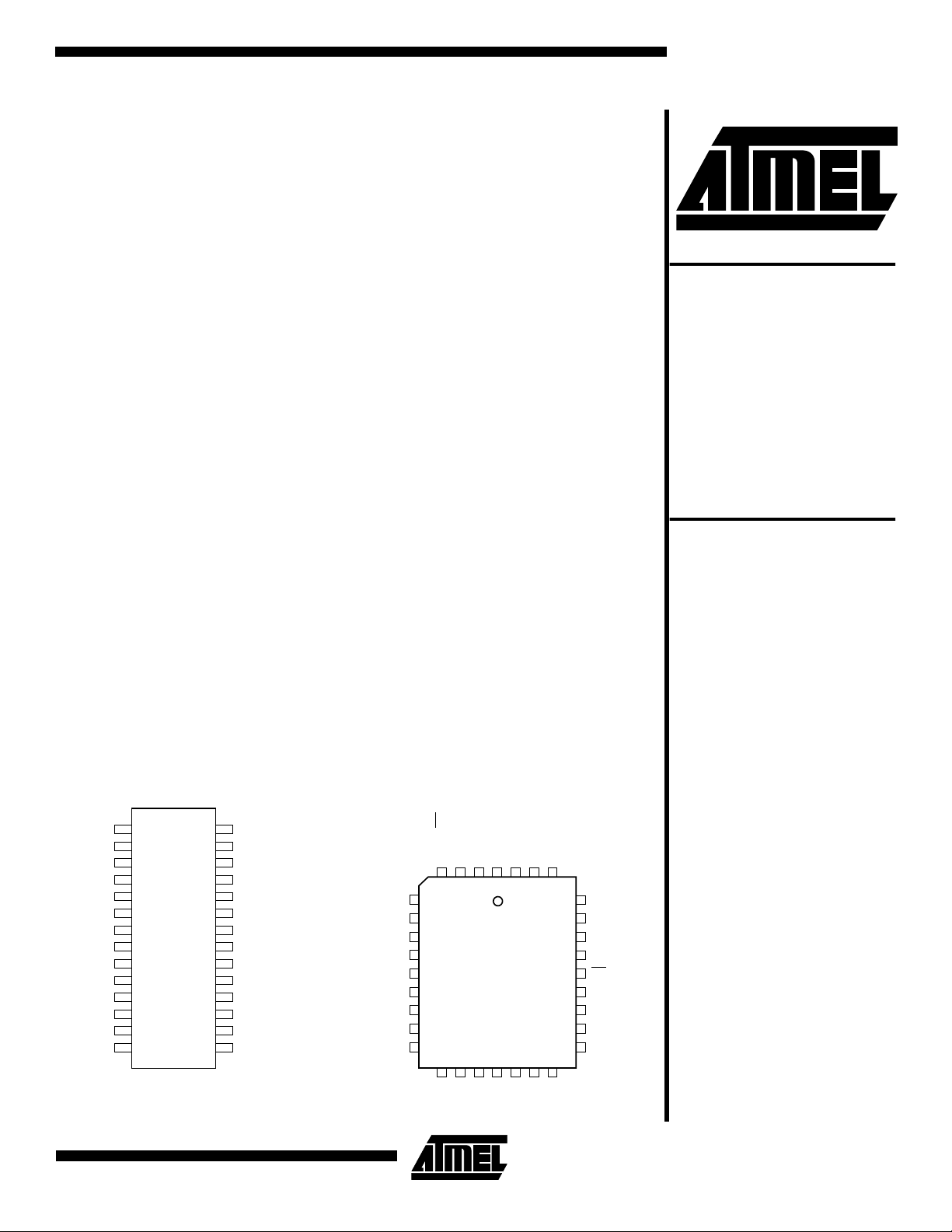
Pin Configurations
GND
TEST1
RESET
SDI/P1.1
SDO/P1.0
TEST2
NC
NC
NC
NC
NC
NC
NC
NC
SOIC Top View
1
2
3
4
5
6
7
8
9
10
11
12
13
14
28
27
26
25
24
23
22
21
20
19
18
17
16
15
VCC
P1.2/DTR
P1.3/SCK
P1.4/DSR
NC
NC
NC
NC
NC
NC
NC
NC
NC
NC
P1.0/SDO
TEST2
NC
NC
NC
NC
NC
NC
NC
PLCC Top View
P1.1/SDI
RESET
TEST1
GND
432
5
6
7
8
9
10
11
12
13
14151617181920
1
VCC
P1.2/DTR
P1.3/SCK
323130
29
28
27
26
25
24
23
22
21
P1.4/DSR
NC
NC
NC
NC
NC
NC
NC
NC
132K Bytes
Flash Data
Memory
AT89S4D12
NCNCNCNCNCNCNC
0921A-A–12/97
4-281

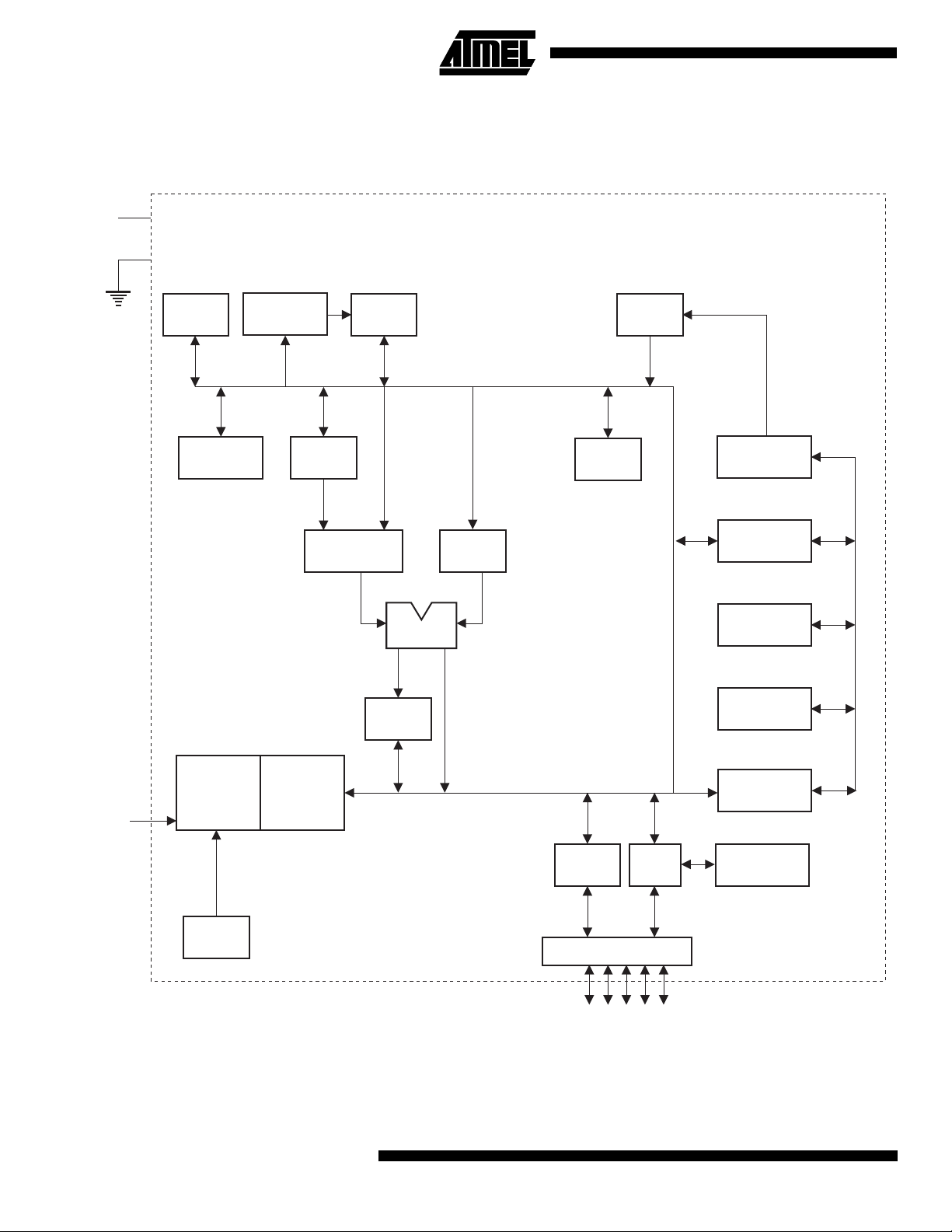
Block Diagram
V
CC
GND
128K
Flash
REGISTER
B
RAM ADDR.
REGISTER
RAM
ACC
TMP2 TMP1
ALU
PSW
STACK
POINTER
4K
FLASH
PROGRAM
ADDRESS
REGISTER
BUFFER
PC
INCREMENTER
PROGRAM
COUNTER
4-282
RST
TIMING
AND
CONTROL
12MHz
OSC
INSTRUCTION
REGISTER
AT89S4D12
PORT 1
LATCH
PORT 1 DRIVERS
P1.0 - P1.4
SPI
PORT
DPTR
PROGRAM
LOGIC

AT89S4D12
Pin Description
V
CC
Supply voltage.
GND
Ground.
Port 1
Port 1 is a 5-bit bidirectional I/O port with internal pullups .
The Port 1 output buffers can sink/source four TTL inputs.
When 1s are written to Port 1 pins , they are p ulled hi gh by
the internal pullups and can be used as inputs. As inputs ,
Port 1 pins that are externally being pulled low will source
current (I
In addition, P1.0, P1.1, and P1.3 can be configured as the
SPI data output, data input and shift clock inp ut pins, as
shown in the following table.
Port Pin Alternate Functions
P1.0 SDO (data output pin for SPI channel)
P1.1 SDI (data input pin for SPI channel)
P1.3 SCK (clock input pin for SPI channel)
RST
Reset input. A high on this pin for two machine cycles while
the oscillator is running resets the device.
TEST1
TEST1 is set to V
gram or data memory. This pin can be left unconnected or
tied to ground during normal operation.
TEST2
Test input. This pin has no us er availa ble functio n and can
be left unconnected or tied to ground.
) because of the internal pullups.
IL
during downloading of the Flash pro-
CC
Special Function Registers
A map of the on-chip memory area called the Special Function Register (SFR) space is shown in Table 1.
Note that not all of the addre sses are occupi ed, and unoccupied addresses may not be implemented on the chip.
Read accesses to these addresses will in general return
random data, and write accesses will have an indeterminate effect.
User software should not write 1s to these unlisted locations, since they may be used in future products to invoke
new features. In th at case, th e reset or inac tive valu es of
the new bits will always be 0.
Memory Control Register
the RDY/BSY
bit A16, for the 128K bytes of on-chip Flash data memory.
SPI Regist er s
eral Interface are contained in registers SPCR (shown in
Table 3) and SPSR (shown in Table 4). The SPI data bits
are contained in the SPDR register. Writing the SPI data
register during serial data transfer sets the Write Collision
bit, WCOL, in the SPSR register. The SPDR is double buffered for writing and the values in SPDR are not changed by
Reset.
Dual Data Pointer Registers
two banks of 16-bit Data Pointer Registers are provided:
DP0 at SFR address locations 82H - 83H and DP1 at 84H 85H. Bit DPS = 0 in SFR MC ON selec ts DP0 and DPS = 1
selects DP1. The user should always initialize the DPS bit
to the appropriate value before accessing the respective
Data Pointer register.
flag and the most significant Flash address
Control and status bits for the Serial Periph-
The MCON register contains
To facilitate data transfer,
4-283

Table 1.
0F8H 0FFH
AT89S4D12 SFR Map and Reset Values
0F0H
0E8H 0EFH
0E0H
0D8H 0DFH
0D0H
0C8H 0CFH
0C0H 0C7H
0B8H 0BFH
0B0H 0B7H
0A8H
0A0H 0A7H
B
00000000
ACC
00000000
PSW
00000000
SPSR
00000000
SPCR
000X01XX
0F7H
0E7H
0D7H
0AFH
98H 9FH
90H
88H 8FH
80H
P1
XXX11111
DP0L
00000000
DP0H
00000000
DP1L
00000000
DP1H
0000000
MCON
XXXXX010
SPDR
XXXXXXXX
PCON
0XXX0000
97H
87H
4-284
AT89S4D12
 Loading...