


AT89RFD-10 / EVLB002
Non-Dimmable Fluorescent Ballast
..........................................................................................................................................................
User Guide IXDN0037

Ballast Demonstrator User Guide -1
7629A–AVR–04/06
Section 1
Introduction...........................................................................................1-1
1.1 General Description .................................................................................1-2
1.2 Ballast Demonstrator Features ................................................................1-2
Section 2
Ballast Demonstrator Device Features ................................................2-5
2.1 Atmel Supported Products .......................................................................2-5
2.2 IXYS Supported Products ........................................................................2-5
Section 3
Ballast Description ...............................................................................3-7
3.1 Circuit Topology .......................................................................................3-7
3.1.1 Line Conditioning ...............................................................................3-7
3.1.2 Low Voltage Supply .................................. ... .... ... ... ... ... .... ... ... ... .........3-7
3.1.3 PFC Boost Regulator .........................................................................3-8
3.1.4 PFC Magnetics ..................................................................................3-8
3.1.5 Lamp Drive ........................................................................................3-8
3.1.6 Control ................................... ............................................................ 3-8
3.1.7 IXYS IXI859 Charge Pump Regulator ...............................................3-9
3.1.8 IXYS IXTP02N50D Depletion Mode MOSFET used ..........................3-9
3.1.9 IXYS IXD611 Half bridge MOSFET driver .......................................3-10
3.1.10 IXYS IXTP3N50P PolarHV N-Channel Power MOSFET .................3-10
Section 4
Circuit Operation.................................................................................4-11
4.1 PFC ................................. .......................................................... .............4-11
4.1.1 PFC Sequence ................................................................................4-12
4.2 Lamp Circuit ...........................................................................................4-12
4.2.1 General .................................. .......................................... ................4-12
Section 5
AT8xEB5114 Non-dimmable Software...............................................5-15
5.1 Main_AT8xEB5114_fluo_demo.c ..........................................................5-17
5.1.1 ADC STATE MACHINE ...................................................................5-17
5.2 Pfc_ctrl.c ................................................................................................5-19
5.2.1 PFC STATE MACHINE ...................................................................5-19
5.3.1 Lamp State Machine ........................................................................5-21
Section 6
Conclusion .........................................................................................6-23

-2 Ballast Demonstrator User Guide
7629A–AVR–04/06
6.1 Appendix 1: Capacitor Coupled Low Voltage Supply .............................6-23
6.2 Appendix 2: PFC Basics .........................................................................6-24
6.3 Appendix 3: Bill of Materials....................................................................6-25
6.4 Appendix 4: Schematic .......... .... ... ... ... ... .... ... ... ... .... ... ... ... ... .... ... ... ... .... ...6-28
Ballast Demonstrator User Guide -1
7629A–AVR–04/06
Section 1
Introduction
Efficient fluorescent lamps and magnetic ballasts have been the standard lighting fixture
in commercial and industrial lighting for many years. Several lamp types, rapid start,
high output, and others are available for cost effective and special applications. This
user guide covers operation and development details of the non-dimmable version of
our fluorescent ballast for operating a va riety of lamps that are available today. This
guide also covers power electronic circuits that find wide utilization in other applications
beyond lighting alone, which include Power Factor Correction, Half-Bridge Inverter
Drives, and Charge Pump Regulators all employing a variety of IXYS / Atmel parts.
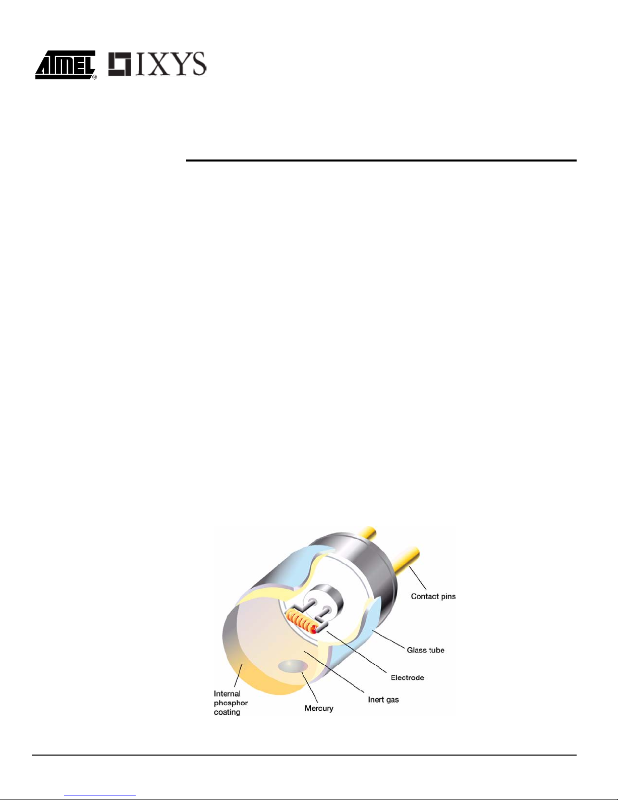
Typical rapid start fluorescent lamps have two pins at each end with a filament across
the pins. The lamp has argon gas under low pressure and a small amount of mercury in
the phosphor coated glass tube. As an AC voltage is applied at each end and the filaments are heated, electrons are driven off the filaments that collide with mercury atoms
in the gas mixture. A mercury electron reaches a higher energy level then falls back to a
normal state releasing a photon of ultraviolet (UV) wavelength. This photon collides with
both argon assisting ionization and the phosphor coated glass tube. High voltage and
UV photons ionize the argon, increasing gas conduction and releasing more UV photons. UV photons collide with the phosphor atoms increasing their electron energy state
and releasing heat. Phosphor electron state decreases and releases a visible light photon. Different phosphor and gas materials can modify some of the lamp characteristics.
Figure 1-1. Fluorescent Tube Composition

-2 Ballast Demonstrator User Guide
7629A–AVR–04/06
Since the argon conductivity increases and resistance across the lamp ends decrease s
as the gas becomes excited, an inductance (ballast) must be used to limit and control
the gas current. In the past, an inductor could be designed to limit the current for a narrow range of mains voltage and frequency. A better method to control gas current is to
vary an inductor's volt-seconds to achieve th e d esired lamp current and in tensity. A va riable frequency inverter operating from a DC bus can do this. If the inductor is part of an
R-L-C circuit, rapid start ignition and operating currents are easily controlled depending
on the driving frequency versus resonant frequency.
Utility is enhanced by designing a power factor correcting boost conve rter (PFC) to
achieve the inverter DC bus over a wide mains voltage ra nge of 90 - 265VAC, 50/60 Hz.
Since a PFC circuit keeps the mains current and voltage in phase with very low distortion, mains power integrity is maintained. Additional utility is achieved by designing a
microcontroller for the electronic ballast application tha t can precisely and eff iciently
control power levels in the fluorescent lamp. An application specific microcontroller
offers the designer unlimited opportunity to enhance marketability of lighting products.
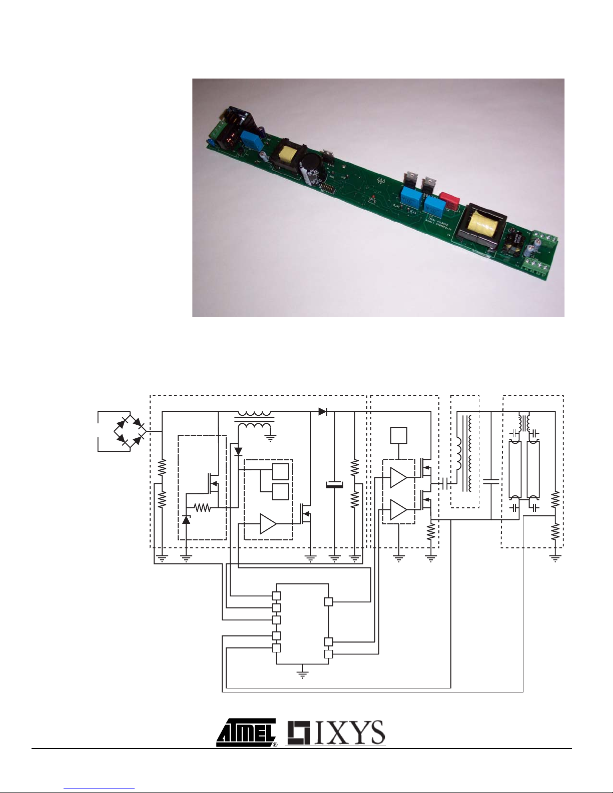
The final design topology is shown in the block diagram of Figure 1-3.
1.1 General
Description
Fluorescent ballast topology usually includes line conditioning for CE compliance, a
power factor correction block including a boost converter to 380 V for universal input
applications and a half bridge inverter. Varying the fr equency of the inverter permits time
for filament preheat and ignition for rapid starting, including precise power control. As
shown in the block diagram, figure 3, all of these functions can be timed, regulated, and
diagnosed with the Atmel AT89EB5114 microcontroller.
1.2 Ballast
Demonstrator
Features
• Automatic microcontroller non-dimmable ballast
• Universal input _ 90 to 265 VAC 50/60 Hz, 90 to 370 VDC
• Power Factor Corrected (PFC) boost regulator
• Power feedback for stable operation over line voltage range
• Variable frequency half bridge inverter
• 18W, up to 2 type T8 lamps
• Automatic single lamp operation
Ballast Demonstrator User Guide -3
7629A–AVR–04/06
Figure 1-2. Ballast demonstrator assembled board
Figure 1-3. Non-Dimmable Ballast block diagram
UVLO
15V
3.3V
Regulator
PFC Driver
IX859
PFC BOOST REGULATOR
Driver
Driver
15V
INVERTER
DECOUPLING CAPACITOR
RESONATING
INDUCTOR
AND
FILAMENT
TRANSFORMER
2
11
3
10
5
8
6
7
T4
IXD611
R28
IXTP3N50P
Q5
Q4
BULK CAPACITOR
C9
C14
D4
Q3
R2
Q1
D2
D3
R9
&
R13
R35
T1
IXTP02N50D
R10
&
R14
R39
11
2
10
3
56
7
C11
RESONATING CAPACITOR
T3
BALANCE
TRANSFORMER
AND
LAMPS
POWER
V
OLTAGE
R42
PFC Output
Inverter High
Inverter Low
V_HAVERSINE
V_BUS
V_LAMP
I_LAMP
P3.5/W0M1
P3.5W1M0
P3.6/W1M1
P4.0/AIN0
P3.3/AIN4
P4.1/AIN1
P4.3/AIN3
PFC_ZCD
P3.2/INT0
AT89EB5114
8
12
1
PFC Inductor

Ballast Demonstrator User Guide -5
7629A–AVR–04/06
Section 2
Ballast Demonstrator Device Features
2.1 Atmel Supported
Products
AT89EB5114 Microcontroller
• High speed configurable PWM outputs for PFC and ½ bridge inverter
• 6 Analog inputs for A/D conversion, 2.4V internal reference level
• 3 High speed PWM outputs used for the PFC and ½ bridge driver
• A/D with programmable gain used for efficient current sensing
• SOIC 20 pin package
2.2 IXYS Supported
Products
IXI859 Charge pump with voltage regulator and MOSFET driver
• 3.3V regulator with undervoltage lockout
• Converts PFC energy to regulated 15VDC
• Low propagation delay driver with 15V out and 3V input for PFC FET gate
IXTP3N50P MOSFET
• 500V, low R
DS
(ON) power MOSFET, 3 used in design
IXD611S MOSFET driver
• Up to 600mA drive current
• ½ bridge, high and low side driver in a single surface mount IC
• Undervoltage lockout

Ballast Demonstrator User Guide -7
7629A–AVR–04/06
Section 3
Ballast Description
3.1 Circuit Topology • Line conditioning with input filter and varistor for noise suppression and protection.
• Low Voltage supply
• PFC / boost regulator
• PFC magnetics
• Lamp drive
• Microprocessor control
• Charge pump regulator
• ½ bridge driver
• ½ bridge power MOSFET stage for up to 2 lamps
3.1.1 Line Conditioning An input filter section consisting of C1, C3, and common mode choke L1 prevent switch-
ing signal frequencies and their harmonics from the PFC boost converter from being
conducted to the mains. Varistor RV1 protects the ballast circuit from line voltage transients. Full wave bridge rectifier BR1 converts the line AC t o a DC h aversine. Diode D 2
is used to provide a point ahead of the boost inductor and filter where the haversine signal can be sensed by the microcontroller. This is necessary for the proper timing of the
PFC control drive signal which must maintain a constant ON time pulse width over a
haversine period.
3.1.2 Low Voltage Supply 3.3V microco ntroller po wer an d ~ 15V F ET drive power ar e prov ided by t he low volta ge
supply consisting of a current source (Q1) and multipurpose IC U1 (IXI589). Internal to
U1 are a 3.3V linear regulator, a 15V (nominal) two point regulator, under-voltage lockout comparators and control, charge pump switching circuitry, and a FET driver. (See
more detailed description of the IXI859 below) For startup, the current source formed by
Q1, and its associated components sources current into C6 until the voltage at U1 pin 1
reaches the under-voltage lockout upper lim it of approximately 14.1V. The current
source voltage output is limited by zener diode D3 to about 16 V. When the under-voltage lockout limit is reached, the IXI859 begins to supply 3.3V to the microcon troller. The
microcontroller then begins to supply drive pulses to the PF C FET Q3 through the
IXI859 FET gate driver. The charge pump regulator circuit is then able to supply 15V
power by efficiently converting energy from the PFC switching circuit. This feature is not
used in the non-dimmable demonstrator design. Rather, a voltage doubler circuit consisting of D4, D20 and C31 connected to the PFC transformer secondary provides 15V
power after startup.

-8 Ballast Demonstrator User Guide
7629A–AVR–04/06
3.1.3 PFC Boost
Regulator
The PFC (Power Factor Correcting) boost regulato r circuit is used to convert the rect ified input line voltage to a 380V DC supply while maintaining a sinusoidal average input
current in phase with the input voltage. The microcontroller accomplishes this by switching the PFC FET with ON times that are constant over a haversine period and by
maintaining nearly critical conduction conditions. Since the current in the PFC inductor
is nearly triangular and its peaks are proportional to the input haversine voltage, the
average current is proportional to the input waveform. Therefore, the power factor is
maintained near unity.
3.1.4 PFC Magnetics Without going into the derivations of the formu las used, the transformer de sign is as
follows:
L = [(1.4 * 90VAC) * (20 uS)] / 3.6A peak = 700 uH
A 3.6 Apk maximum FET current is 1.8 A approximately divided by the ON/OFF ratio.
The ON time has been discussed earlier and the OFF time maximum will occur at high
line condition at the peak of the haversine. A 16 mm core was chosen for the recommended power density at 200 mT and 50 KHz.
3.1.5 Lamp Drive The microcontroller sends rectangular pulses to the half-bridge driver (IXD611). Th e
IXD611 contains high side and low side FET drivers and floating high side supply circuitry to produce high side gate drive. (See more detailed description of the IXD611 to
follow) The pulses from the microcontroller are non-overlapping and 180 degrees out of
phase. A deadband time between HBRIDGE HI and HBRIDGE LO pulses insures that
both drivers are never on at the same time. The lamp drive is constant in duty cycle. The
power to the lamps is controlled by varying the frequency of the drive signals. The
IXD611 drives two FETs (IXTP3N50P) in a half-bridge configuration.
The output of the half-bridge is AC coupled by C11 to the lamps through a resonating
transformer and capacitor (T4 and C12). Additional windings on T4 supply filament current to the lamps. Balance transformer T3 forces the current to be shared equally by the
two lamps. The lamp currents are conducted to circuit common through a 1 Ohm resistor which is used to sense the lamp current so that lamp power may be controlled by the
microcontroller.
3.1.6 Control The ballast is controlled by microcontroller U3. U3 is an Atmel AT8xEB5114 with an
80C51 core and specialized circuitry for controlling the ballast. Included are two PWM
units that are used for controlling the PFC drive and the half-bridge drive with deadtime.
An internal analog to digital converter converts input signals so the processor can monitor and control the ballast.
The AT8xEB5114 pin connections for ballast control and scale factors for analog inputs
are as follows:
• P4.0/AIN0 VBus monitor input (VBus = AIN0 x 201)
• P4.1/AIN1 Rectified Lamp Voltage Sense (Vlamp = AIN1 x 294)
• P4.2/AIN2 Lamp AC Voltage (VAC ~= AIN2 x 446)
• P4.3/AIN3 Lamp Current (Amplify by 10) (Ilamp = AIN3/1Ohm)
• P3.3/AIN4 Haversine Voltage input (Vhaversine = AIN4 x 201)
• P3.4/AIN5 Temperature sensor (Vtemp = 1.1V @ 25C || .264V @ 85C)
• P3.6 NC (No Connection)
• P3.5/W1M0 PFC Drive
• P3.2/INT0 Current Zero Crossing Detect (Interrupt)
• P3.1/W0M1 Half Bridge high side drive

Ballast Demonstrator User Guide -9
7629A–AVR–04/06
• P3.0/W0M0 Half Bridge low side drive
The Temperature monitor is a thermistor with a nominal 10K resistance at 25°C and
1.74K resistance at 80°C. It is mounted o n the circuit board and so monitors ambient
temperature in the lamp housing.
Additional dedicated pins allow in-circuit progr amming of the flash memory using h eader
J2. Other pins provide connections for the oscillator and voltage reference components.
3.1.7 IXYS IXI859 Charge
Pump Regulator
The IXI859 charge pump regulator integrates three primary functions central to the PFC
stage of the ballast demonstrator. First it includes a linear regulated supply voltage output, and in this application the linear regulator provides 3.3V to run the microcontroller.
The second function is a gate drive buffer that switches an external power MOSFET
used to boost the PFC voltage to 380V. Once the microcontroller is booted up and running, it generates the input signal to drive the PFC MOSFET through the IXI859 gate
drive buffer. Finally, the third function provides two point regulated supply voltage for
operating external devices. As a safety feature, the IXI859 includes an internal Vcc
clamp to prevent damage to itself due to over-voltage conditions.
In general applications at start-up, an R-C combination is employed at the Vcc supply
pin that ramps up a trickle voltage to the Vcc pin from a high voltage offline source. The
value of R is large to protect the internal zener diode clamp and as a result, can't supply
enough current to power the microcontroller on it's own. C provides energy to boot the
microcontroller. At a certain voltage level during the ramp up, the Under Voltage Lock
Out point is reached and the IXI859 enables itself. The internal voltage regulator that
supplies the microcontroller is also activated during this time. However, given the trickle
charge nature of the Vcc input voltage, the microcontroller must boot itself up and
enable PFC operation to provide charge pump power to itself. This means that the R-C
combination must be sized carefully so that the voltage present at the Vcc pin does not
collapse too quickly under load and causes the UVLO circuitry to disable device operation before the microcontroller can take over the charge pump operation. There are a
couple of problems associated with this method. Namely, under normal operation as
previously mentioned, the internal zener diode clamps the input Vcc pin voltage and R
must dissipate power as long as the zener diode is clamped. Assuming that a rectified
sine wave is supplied at the Vcc means that the internal zener will be clamped and R will
be dissipating power as long as the input voltage is greater than the zener voltage.
Another problem is that when a universal range is used at the Vcc pin, 90-265V, R must
dissipate nine times the power, current squared function for power in R, o ver a threefold increase of voltage from 90V at the low end to 265V on the high end.
As an alternative and as used in the ballast demonstrator, the Vcc pin is fed voltage by
way of a constant current source. This circuit brings several advantages over the regular
R-C usage. First we can reduce power consumed previously by R and replace it with a
circuit that can provide power at startup and once the microcontroller is running, shut off
current into the Vcc pin. The constant current source also has the ability to provide sufficient power to run the microcontroller unlike the R-C combination. This would be an
advantage in the case that a standby mode is desired. Overall power consumption can
be reduced by allowing the microcontroller to enter a low power mode and shut down
PFC operation without having to reboot the microcontroller. Since the R-C combination
cannot provide enough power to sustain microcontroller operation, the microcontroller
must stay active running the PFC section to power itself.
3.1.8 IXYS IXTP02N50D
Depletion Mode
MOSFET used as a
current source
The IXYS IXTP02N50D depletion mode MOSFET is used in this circuit to provide power
and a start-up voltage to the Vcc pin of the IXI859 charge pump regulator. The
IXTP02N50D acts as a current source and self regulates as the source voltage rises
above the 15V zener voltage and causes the gate to becom e more negative than the
 Loading...