

ATMEL AT89LV52-12PI, AT89LV52-12PC, AT89LV52-12JI, AT89LV52-12JC, AT89LV52-12AI Datasheet
...
Features
•
Compatible with MCS-51™ Products
•
8K Bytes of Reprogrammable Flash Memory
– Endurance: 1,000 Write/Erase Cycles
•
2.7V to 6V Operating Range
•
Fully Static Operation: 0 Hz to 12 MHz
•
Three-Level Program Memory Lock
•
256 x 8-Bit Internal RAM
•
32 Programmable I/O Lines
•
Three 16-Bit Timer/Counters
•
Eight Interrupt Sources
•
Programmable Serial Channel
•
Low Power Idle and Power Down Modes
8-Bit
Microcontroller
Description
The AT89LV52 is a low-voltage, high-performance CMOS 8-bit microcomputer with
8K bytes of Flash programmable and erasable read only memory. The device is manufactured using Atmel’s high density nonvolatile memory technology and is compatible with the industry standard 80C51 and 80C52 instruction set and pinout. The onchip Flash allows the p rogram memor y to be repr ogrammed in- system or by a conventional nonvolatile memory programmer. By combi ning a versati le 8-bit CPU with
Flash on a monolithic chip, the Atmel AT89LV52 is a powerful microcomputer which
provides a highly flex ible and co st effe ctive solu tion to many embedd ed con trol app lications. The AT89LV52 operates at 2.7 volts up to 6.0 volts.
(continued)
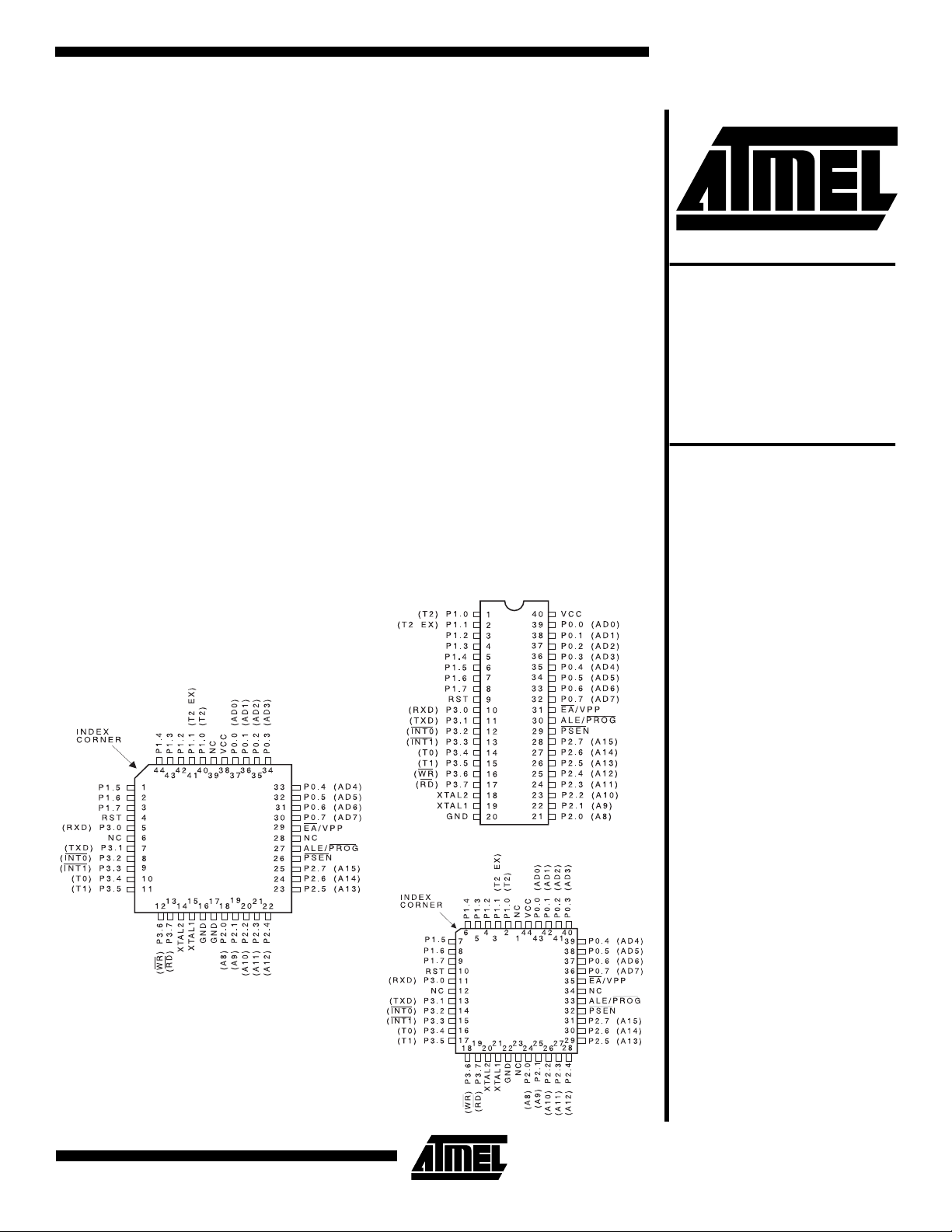
Pin Configurations
TQFP
PDIP
with 8K Bytes
Flash
AT89LV52
PLCC
0375D-E–12/97
4-83
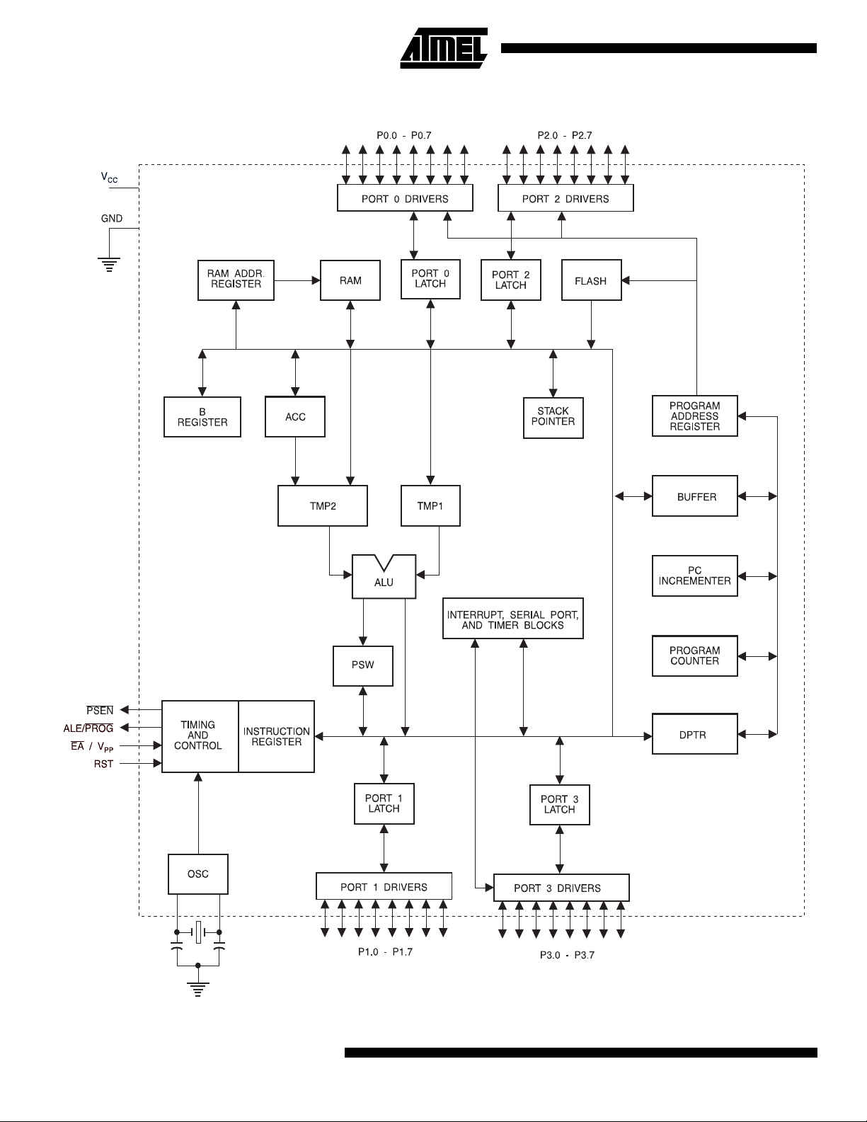
Block Diagram
4-84
AT89LV52
AT89LV52
The AT89LV52 provides the following standard features:
8K bytes of Flash, 256 bytes of RAM, 32 I/O lines, three 16bit timer/counters, a six-vector two-level interrupt architecture, a full duplex serial port, on -chip oscillat or, and clock
circuitry. In addition, the AT89LV52 is designed with static
logic for operation down to zero frequency an d supports
two software select able power saving mo des. The Idle
Mode stops the CPU while allowing the RAM,
timer/counters, serial p or t, and int er rupt s yst em to co nti nue
functioning. The Power Down Mode saves the RAM contents but freezes the oscillator, disabling all other chip functions until the next hardware reset.
Pin Description
V
CC
Supply voltage.
GND
Ground.
Port 0
Port 0 is an 8-bit open drain bidirectional I/O port. As an
output port, each pin can sink eight TTL inputs. When 1s
are written to port 0 pins, the pins can be used as highimpedance inputs.
Port 0 can also be configu red to be the multiplex ed loworder address/data bus during accesses to ex ternal program and data memory. In this mode, P0 has internal pullups.
Port 0 also rece ives th e code by tes dur ing Fla sh prog ramming and outputs the code bytes during program ver ification. External pu llups are requ ired during pr ogram v erific ation.
Port 1
Port 1 is an 8-bit bidire ction al I/O por t w ith inter nal pullu ps.
The Port 1 output buffers can sink/source four TTL inputs.
When 1s are written to Port 1 pins , they are p ulled hi gh by
the internal pullups and can be used as inputs. As inputs ,
Port 1 pins that are externally being pulled low will source
current (I
In addition, P1.0 and P1. 1 can be configured to be the
timer/counter 2 external count input (P1.0/T2) and the
timer/counter 2 trigger input (P1.1/T2EX), respectively, as
shown in the following table.
Port Pin Alternate Functions
P1.0 T2 (external count input to
P1.1 T2EX (Timer/Counter 2 capture/reload
Port 1 also receives the low-order address bytes during
Flash programming and verification.
) because of the internal pullups.
IL
Timer/Counter 2), clock-out
trigger and direction control)
Port 2
Port 2 is an 8-bit bidirectional I/O port with interna l pullups.
The Port 2 output buffers can sink/source four TTL inputs.
When 1s are writte n to Po rt 2 pi ns, they a re pul led high by
the internal pullups and can be used as inputs. As inputs,
Port 2 pins that are externally being pulled low will source
current (I
) because of the internal pullups.
IL
Port 2 emits the high-order address byte during fetches
from external program memory and during accesses to
external data memory th at u se 16 -b it a ddres s es ( MO VX @
DPTR). In this application, Port 2 uses strong internal pullups when emitting 1s. During accesses to external data
memory that use 8-bit addresses (MOVX @ RI), Port 2
emits the contents of the P2 Special Function Register.
Port 2 also receives the high-order address bits and some
control signals during Flash programming and verification.
Port 3
Port 3 is an 8-bit bidirectional I/O port with interna l pullups.
The Port 3 output buffers can sink/source four TTL inputs.
When 1s are writte n to Po rt 3 pi ns, they a re pul led high by
the internal pullups and can be used as inputs. As inputs,
Port 3 pins that are externally being pulled low will source
current (I
) because of the pullups.
IL
Port 3 also serv es t he fun ctions of v arious spe cial f eatures
of the AT89LV51, as shown in the following table.
Port Pin Alternate Functions
P3.0 RXD (serial input port)
P3.1 TXD (serial output port)
P3.2 INT0 (external interrupt 0)
P3.3 INT1
P3.4 T0 (timer 0 external input)
P3.5 T1 (timer 1 external input)
P3.6 WR
P3.7 RD
(external interrupt 1)
(external data memory write strobe)
(external data memory read strobe)
Port 3 also receives some control signals for Flash programming and verification.
RST
Reset input. A high on this pin for two machine cycles while
the oscillator is running resets the device.
ALE/PROG
Address Latch Enable is an output pulse for latching the
low byte of the address during accesses to external memory. This pi n is al so t h e pr og ra m pu l se in p ut (PROG
) during
Flash programming.
In normal operation, ALE is emitted at a constant rate of 1/6
the oscillator frequency and may be used for external timing or clocking purposes. Note, however, that one ALE
4-85

pulse is skipped durin g each access to exte rnal data me mory.
If desired, ALE operation can be disabled by setting bit 0 of
SFR location 8EH. With the bit set, ALE is active only during a MOVX or MOVC instruction. Otherwise, the pin is
weakly pulled high. Setting the ALE-disable bit has no
effect if the microcontroller is in external execution mode.
PSEN
Program Store Enable is the read strobe to external pro-
gram memory.
When the AT89LV52 is executing code from external pro-
gram memory, PSEN
cycle, except that two PSEN
is activated twice each machine
activations are skipped during
each access to external data memory.
/V
EA
PP
External Access Enable. EA must be strapped to GN D in
order to enable the device to fetch code from external program memory locations starting at 0000H up to FFFFH.
Note, however, that if lock bit 1 is programmed, EA
will be
internally latched on reset.
should be strapped to VCC for internal program execu-
EA
tions.
This pin also receives the 12-volt programming enable voltage (V
) during Flash programming when 12-volt pro-
PP
gramming is selected.
XTAL1
Input to the inverting oscillator am plifier and input to the
internal clock operating circuit.
XTAL2
Output from the inverting oscillator amplifier.
Table 1.
0D8H 0DFH
0D0H PSW
0C8H T2CON
0C0H 0C7H
0B8H IP
0B0H P3
0A8H IE
0A0H P2
AT89LV52 SFR Map and Reset Values
0F8H 0FFH
0F0H
0E8H 0EFH
0E0H ACC
98H SCON
90H P1
88H TCON
80H P0
B
00000000
00000000
00000000
00000000
XX000000
11111111
0X000000
11111111
00000000
11111111
00000000
11111111
T2MOD
XXXXXX00
SBUF
XXXXXXXX
TMOD
00000000
SP
00000111
RCAP2L
00000000
TL0
00000000
DPL
00000000
RCAP2H
00000000
TL1
00000000
DPH
00000000
TL2
00000000
TH0
00000000
TH2
00000000
TH1
00000000
PCON
0XXX0000
0F7H
0E7H
0D7H
0CFH
0BFH
0B7H
0AFH
0A7H
9FH
97H
8FH
87H
4-86
AT89LV52
AT89LV52
Special Function Registers
A map of the on-chip memory area called the Special Function Register (SFR) space is shown in Table 1.
Note that not all of the addresses are occupied, and unoccupied addresses may not be implemented on the chip.
Read accesses to these addresses will in general return
random data, and write accesses will have an indeterminate effect.
User software should not write 1s to these unlisted locations, since they may be used in future products to invoke
Table 2.
T2CON Address = 0C8H Reset Value = 0000 0000B
Bit Addressable
Symbol Function
TF2 Timer 2 overflow flag set by a Timer 2 overflow and must be cleared by software. TF2 will not be set when either
EXF2 Timer 2 external flag set whe n either a capture or reloa d is c aused b y a negat iv e tr ans ition on T2 EX and EXEN2 = 1.
T2CON—Timer/Counter 2 Control Register
TF2 EXF2 RCLK TCLK EXEN2 TR2 C/T2
Bit76543210
RCLK = 1 or TCLK = 1.
When Timer 2 interrupt is enabled, EXF2 = 1 will cause the CPU to vector to the Timer 2 interrupt routine. EXF2
must be cleared by software. EXF2 does not cause an interrupt in up/down counter mode (DCEN = 1).
new features. In th at case, th e reset or inac tive valu es of
the new bits will always be 0.
Timer 2 Registers
Control and status bits are contained in
registers T2CON (shown in Table 2) and T2MOD (shown in
Table 4) for Timer 2. The register pair (RCAP2H, RCA P2L )
are the Capture/ Reloa d regist ers for Timer 2 i n 16-bit c apture mode or 16-bit auto-reload mode.
Interrupt Registers
The individual interrupt enable b its
are in the IE register. Two priorities can be set for each of
the six interrupt sources in the IP register.
CP/RL2
RCLK Receive clock enable. When set, causes the serial port to use Timer 2 overflow pulses for its receive clock in serial
port Modes 1 and 3. RCLK = 0 causes Timer 1 overflow to be used for the receive clock.
TCLK Transmit clock enable. Wh en set, causes the serial port to use Timer 2 overflow pulses for its transmit clock in serial
port Modes 1 and 3. TCLK = 0 causes Timer 1 overflows to be used for the transmit clock.
EXEN2 Timer 2 external ena ble. When set, al lows a capture or reload to oc cu r as a re sult o f a neg ati ve transition o n T2 EX if
Timer 2 is not being used to clock the serial port. EXEN2 = 0 causes Timer 2 to ignore events at T2EX.
TR2 Start/Stop control for Timer 2. TR2 = 1 starts the timer.
C/T2
CP/RL2
Data Memory
The AT89LV52 implements 256 bytes of on-chip RAM. The
upper 128 bytes oc cupy a parallel ad dress space to the
Special Function Register s. That means the u pper 128
bytes have the same addresses as the SFR space but are
physically separate from SFR space.
When an instruction accesses an internal location above
address 7FH, the address mode used in the instruction
specifies whether the CPU accesses the upper 128 bytes
of RAM or the SFR space. Instructions that use direct
addressing access SFR space.
Timer or counter select for Timer 2. C/T2 = 0 for timer function. C/T2 = 1 for external event counter (falling edge
triggered).
Capture/Reload select. CP/RL2 = 1 causes captures to occur on negative transitio ns at T2EX if EXEN2 = 1. CP/RL2
= 0 causes automatic reloads to o ccur when Ti mer 2 o v erflo ws o r negati ve tran sitions o ccur at T2EX whe n EXEN2 =
1. When either RCLK or TCLK = 1, this bit is ignored and the timer is forced to auto-reload on Timer 2 overflow.
For example, the following direct addressing instruction
accesses the SFR at location 0A0H (which is P2).
MOV 0A0H, #data
Instructions that use indirect addressing access the upper
128 bytes of RAM. For example, the following indirect
addressing inst ructi on, where R0 contains 0A 0H, accesses
the data byte at address 0A0H, rather than P2 (whose
address is 0A0H).
MOV @R0, #data
Note that stack operations are examples of indirect
addressing, so the upper 128 bytes of data RAM are avail able as stack space.
4-87
Timer 0 and 1
Timer 0 and Timer 1 in the AT89LV52 operate the same
way as Timer 0 and Timer 1 in the AT89LV51.
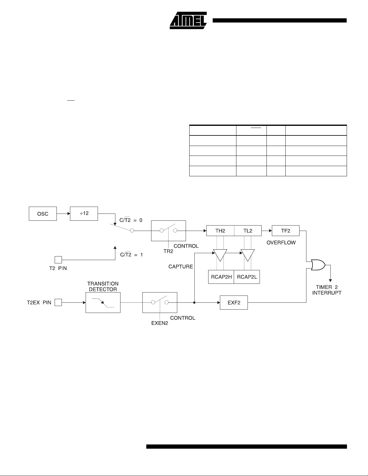
Timer 2
Timer 2 is a 16-bit Timer/Counter that can operate as either
a timer or an event counter. The type of operation is
selected by bit C/T2
Timer 2 has three operating modes: capture, auto-reload
(up or down counting), and baud rate generator. The
modes are selected by bits in T2CON, as shown in Table 3.
Timer 2 consists of two 8- bi t regi st er s, TH2 and TL2. I n the
Timer function, the TL2 r egister is incremented ever y
machine cycle. Since a machine cycle consists of 12 oscillator periods, the count rate is 1/12 of the oscillator frequency.
In the Counter function, the register is incremented in
response to a 1-to-0 transition at its corresponding external
input pin, T2. In thi s func tion, the extern al i nput is sa mpled
in the SFR T2 C ON (sh o w n i n Ta bl e 2).
during S5P2 of every machine cy cle. When the sampl es
show a high in one cycle and a low in the next cycle, the
count is incremented. The new count value appears in the
register during S3P1 of the cycle following the one in which
the transition was detected. Since two machine cycles (24
oscillator perio ds ) ar e re qui red to recognize a 1 -to -0 tr an si tion, the maximum count rate is 1/24 of the oscillator frequency. To ensure that a given level is sampled at least
once before it changes, the level should be held for at least
one full machine cycle.
Table 3.
RCLK + TCLK CP/RL2 TR2 MODE
Timer 2 Operating Modes
0 0 1 16-Bit Auto-Reload
0 1 1 16-Bit Capture
1 X 1 Baud Rate Generator
XX0(Off)
Figure 1.
Timer 2 in Capture Mode
Capture Mode
In the capture mode, two option s are selected by bit
EXEN2 in T2CON. If EXEN2 = 0, Timer 2 is a 16-bit timer
or counter which upon overflow sets bit TF2 in T2CON.
This bit can then be used to generate an interrupt. If
EXEN2 = 1, Timer 2 performs the s ame oper ation, but a 1to-0 transition at external input T2EX also causes the current value in TH2 and TL2 to be captured into RCAP2H and
RCAP2L, resp ective ly. In add ition, th e transi tion at T2E X
causes bit EXF2 in T2CON to b e set. The EX F2 bit, like
TF2, can generate an interrupt. The capture mode is illustrated in Figure 1.
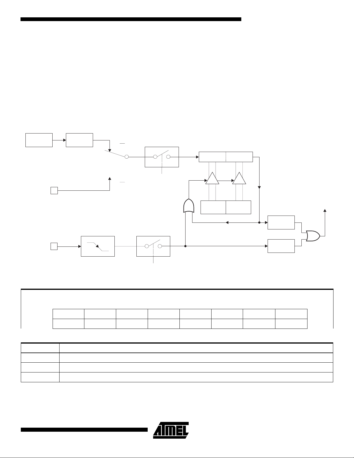
Auto-Reload (Up or Down Counter)
Timer 2 can be programmed to count up or down when
configured in its 16-bit auto-reload mode. This feature is
invoked by the DCEN (Down Counter Enable) bit located in
the SFR T2MOD (see Table 4). Upon reset, the DCEN bit
is set to 0 so that ti mer 2 will defa ult to count u p. When
DCEN is set, Timer 2 can count up o r down, d ependi ng on
the value of the T2EX pin.
Figure 2 shows Timer 2 auto matically counti ng up when
DCEN = 0. In this mode, two options are selected by bit
EXEN2 in T2CON. If EXEN2 = 0, Time r 2 counts up to
0FFFFH and then sets the TF2 bit upon overflow. The overflow also causes the tim er re giste rs to be rel oa ded with the
4-88
AT89LV52
AT89LV52
16-bit value in RCAP2H and RCAP2L. The values in
RCAP2H and RCAP2L ar e pres et by s oftware. If EX EN2 =
1, a 16-bit reload can be triggered either by an overflow or
by a 1-to-0 transition at external input T2EX. This transition
also sets the EXF2 bit. Both th e TF2 and E XF2 bits can
generate an interrupt if enabled.
Setting the DCEN bit enabl es Time r 2 to coun t up o r d own ,
as shown in Figure 3. In this mode, the T2EX pin controls
the direction of the count. A logic 1 at T2EX makes Timer 2
count up. The timer will overflow at 0FFFFH and set the
TF2 bit. This overflow al so causes the 16-bit value in
Figure 2.
Timer 2 Auto Reload Mode (DCEN = 0)
OSC
T2 PIN
÷12
C/T2 = 0
C/T2 = 1
CONTROL
TR2
RELOAD
RCAP2H and RCAP2L to be reloaded into the timer registers, TH2 and TL2, respectively.
A logic 0 at T2EX makes Timer 2 count down. The timer
underflows when TH2 and TL2 equal the values stor ed in
RCAP2H and RCAP2L. The underflow sets the TF2 bit and
causes 0FFFFH to be reloaded into the timer registers.
The EXF2 bit toggles whenever Timer 2 overflows or
underflows and can be used as a 17th bit of resolution. In
this operating mode, EXF2 does not flag an interrupt.
TH2 TL2
OVERFLOW
TIMER 2
RCAP2LRCAP2H
INTERRUPT
TRANSITION
DETECTOR
T2EX PIN
EXEN2
Table 4.
T2MOD Address = 0C9H Reset Value = XXXX XX00B
Not Bit Addressable
Symbol Function
— Not implemented, reserved for future use.
T2OE Timer 2 Output Enable bit.
DCEN When set, this bit allows Timer 2 to be configured as an up/down counter.
T2MOD—Timer 2 Mode Control Register
——————T2OEDCEN
Bit76543210
CONTROL
TF2
EXF2
4-89
 Loading...