

Page 1
8-Bit
Microcontroller
with 8 Kbytes
Flash
AT89C52
Features
Compatible with MCS-51TM Products
•
8 Kbytes of In-System Reprogrammable Fl as h Me mory
•
Endurance: 1,000 Wri te/Erase Cycles
Fully Static Operati on : 0 Hz to 24 MHz
•
Three-Level Program Mem ory Loc k
•
256 x 8-Bit Internal RAM
•
32 Programmable I/O Lines
•
Three 16-Bit Timer/Counters
•
Eight Interrupt Sources
•
Programmable Serial Ch an ne l
•
Low Power Idle and Power Down Modes
•
Description
The AT89C52 is a low-power, high-performance CMOS 8-bit microcomputer with 8
Kbytes of Flash programmable and erasable read only memory (PEROM). The device is manufactured using Atmel’s high density nonvolatile memory tec hnology and
is compatible with the industry standard 80C51 and 80C52 instruction set and pinout.
The on-chip Flash allows the program memory to be reprogrammed in-system or by
a conventional nonvolatile memory programmer. By combining a vers atile 8-bit CPU
with Flash on a monolithic chip, the Atmel AT89C52 is a powerful microcomputer
which provides a highly flexible and cost effective solution to many embedded control
applications.
(continued)
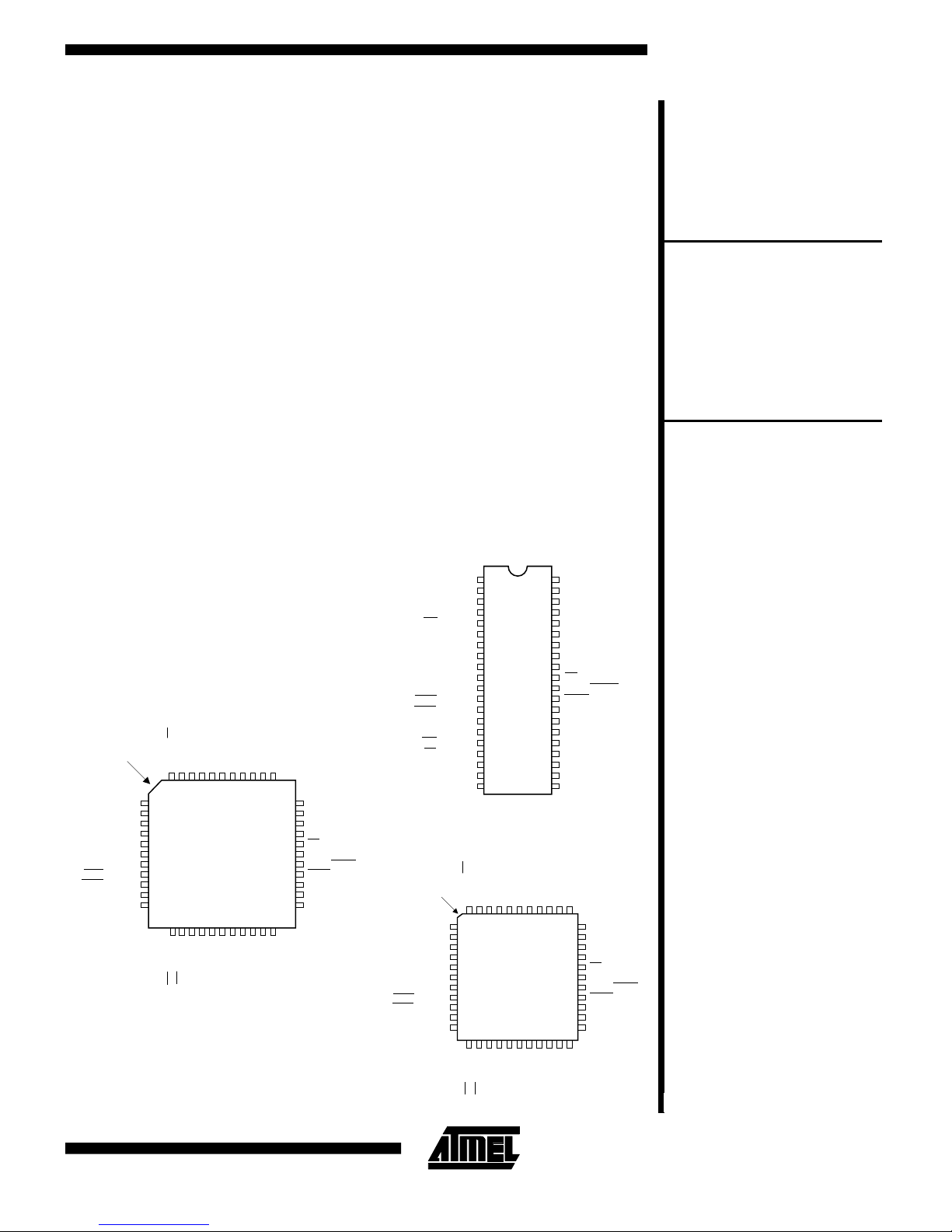
Pin Configurations
PQFP/TQFP
SS)
INDEX
CORNER
(MOSI) P1.5
(MISO) P1.6
(SCK) P1.7
RST
(RXD) P3.0
NC
(TXD) P3.1
(INT0) P3.2
(INT1) P3.3
(T0) P3.4
(T1) P3.5
(
NC
P1.3
P1.2
P1.0 (T2)
VCC
P1.1 (T2 EX)
P1.4
424340
44
1
2
3
4
5
6
7
8
9
10
11
13
12
(WR) P3.6
14
(RD) P3.7
41
15
XTAL2
16
XTAL1
39
17
GND
38
18
GND
(A8) P2.0
37
19
P0.0 (AD0)
P0.1 (AD1)
36
35
21
20
(A9) P2.1
(A10) P2.2
P0.2 (AD2)
P0.3 (AD3)
34
33
32
30
29
28
27
26
25
24
23
22
(A11) P2.3
(A12) P2.4
31
P0.4 (AD4)
P0.5 (AD5)
P0.6 (AD6)
P0.7 (AD7)
EA/VPP
NC
ALE/PROG
PSEN
P2.7 (A15)
P2.6 (A14)
P2.5 (A13)
(T2) P1.0
(T2 EX) P1.1
(SS) P1.4
(MOSI) P1.5
(MISO) P1.6
(SCK) P1.7
(RXD) P3.0
(TXD) P3.1
(INT0) P3.2
(INT1) P3.3
(T0) P3.4
(T1) P3.5
(WR) P3.6
(RD) P3.7 P2.3 (A11)
INDEX
CORNER
(MOSI) P1.5
(MISO) P1.6
(SCK) P1.7
RST
(RXD) P3.0
(TXD) P3.1
(INT0) P3.2
(INT1) P3.3
(T0) P3.4
(T1) P3.5
PDIP/Cerdip
1
2
P1.2
3
P1.3
4
5
6
7
8
RST
9
10
11
12
13
14
15
16
XTAL2 P2.2 (A10)
XTAL1 P2.1 (A9)
17
18
19
GND P2.0 (A8)
20
39
38
37
36
35
34
33
32
31
30
29
28
27
26
25
24
23
22
21
P0.0 (AD0)
P0.1 (AD1)
P0.2 (AD2)
P0.3 (AD3)
P0.4 (AD4)
P0.5 (AD5)
P0.6 (AD6)
P0.7 (AD7)
EA/VPP
ALE/PROG
PSEN
P2.7 (A15)
P2.6 (A14)
P2.5 (A13)
P2.4 (A12)
V
CC
40
PLCC/LCC
SS)
NC
VCC
P0.2 (AD2)
P0.3 (AD3)
P0.1 (AD1)
P0.0 (AD0)
P1.0 (T2)
P1.1 (T2 EX)
P1.2
P1.3
P1.4 (
2
1
23
22
GND
XTAL1
NC
424340
252827
26
(A9) P2.1
(A8) P2.0
41
(A10) P2.2
39
38
37
36
35
34
33
32
31
30
(A11) P2.3
(A12) P2.4
65444
3
7
8
9
10
11
NC
12
13
14
15
16
17 29
21
181920 24
XTAL2
(RD) P3.7
(WR) P3.6
P0.4 (AD4)
P0.5 (AD5)
P0.6 (AD6)
P0.7 (AD7)
EA/VPP
NC
ALE/PROG
PSEN
P2.7 (A15)
P2.6 (A14)
P2.5 (A13)
0313E
Page 2
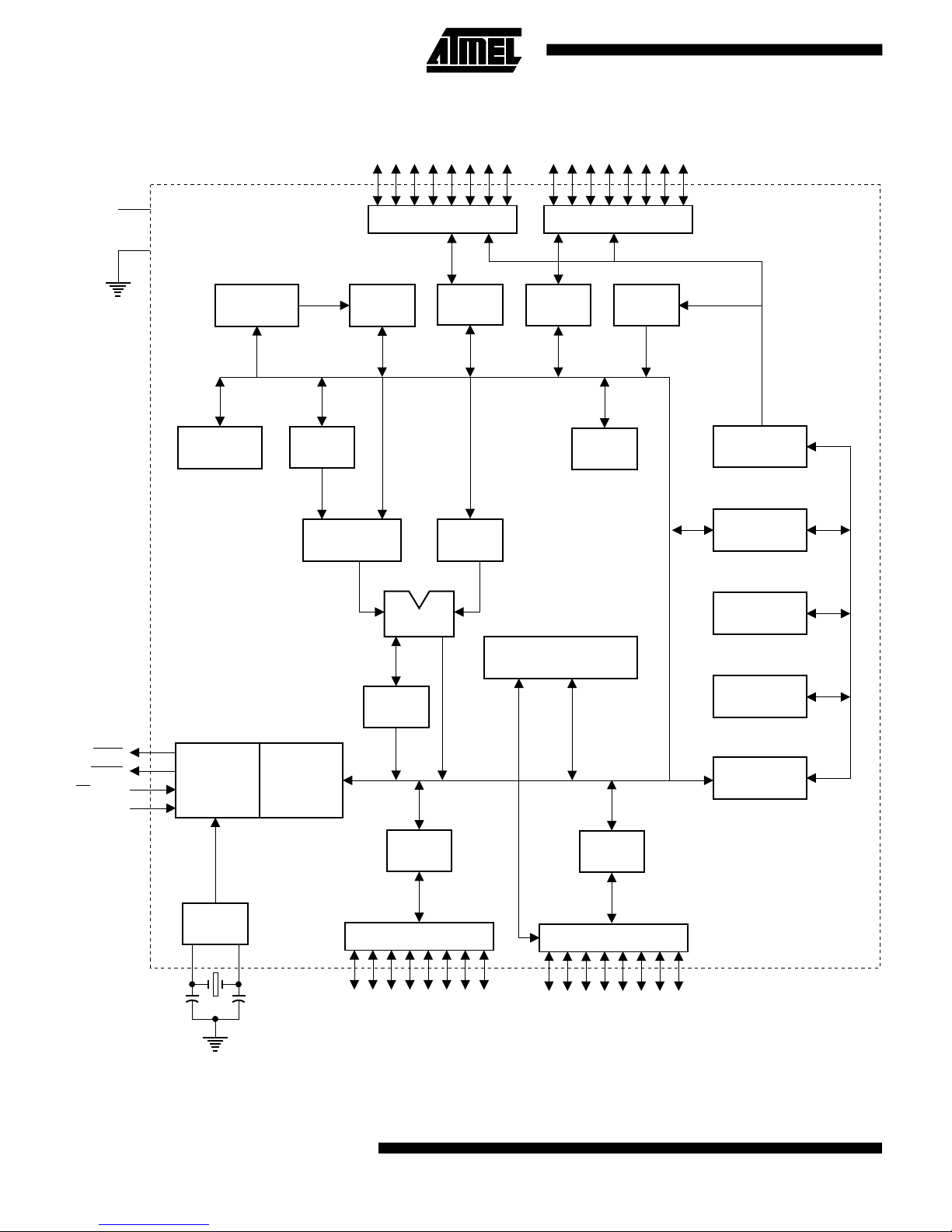
Block Diagram
V
CC
GND
RAM ADDR.
REGISTER
B
REGISTER
ACC
TMP2
P0.0 - P0.7
PORT 0 DRIVERS
RAM
PORT 0
LATCH
TMP1
PORT 2 DRIVERS
PORT 2
LATCH
POINTER
P2.0 - P2.7
FLASH
STACK
PROGRAM
ADDRESS
REGISTER
BUFFER
PSEN
ALE/PROG
EA / V
RST
PC
ALU
INTERRUPT, SERIAL PORT,
AND TIMER BLOCKS
PSW
TIMING
AND
PP
CONTROL
OSC
INSTRUCTION
REGISTER
PORT 1
LATCH
PORT 1 DRIVERS
P1.0 - P1.7
PORT 3
LATCH
PORT 3 DRIVERS
P3.0 - P3.7
INCREMENTER
PROGRAM
COUNTER
DPTR
2 AT89C52
Page 3

(continued)
AT89C52
Description (Continued)
The AT89C52 provides the following standard features: 8
Kbytes of Flash, 256 bytes of RAM, 32 I/O lines , thr ee 16bit timer/counters, a six-vector two-level interr upt architecture, a full duplex serial port, on-chip oscillator, and clock
circuitry. In addition, the AT89C52 is designed with static
logic for operation down to zero frequency and supports
two soft ware selectable p ower saving modes. The Idle
Mode stops the CPU while allowing the RAM, timer/counters, serial port, and interrupt system to continue functioning. The Power Down Mode saves the RAM contents but
freezes the oscillator, disabling all other chip functions until the next hardware reset.
Pin Description
V
CC
Supply voltage.
GND
Ground.
Port 0
Port 0 is an 8-bit open drain bidirectional I/O port. As an
output port, each pin can sink eight TTL inputs. When 1s
are written to port 0 pins, the pins can be used as high-impedance inputs.
Port 0 can also be configured to be the multiplexed low-order address/data bus during accesses to external program and data memory. In this mode, P0 has internal pullups.
Port 0 also receives the code bytes during Flash programming and outputs the code bytes during program verification. External pullups are required during program verification.
Port 1
Port 1 is an 8-bit bidirectional I/O port with internal pullups.
The Port 1 output buffers can sink/source four TTL inputs.
When 1s are written to Port 1 pins, they are pulled high by
the internal pullups and can be used as inputs. As inputs,
Port 1 pins that are externally being pulled low will source
current (I
In addition, P1.0 and P1.1 can be configured to be the
timer/counter 2 external count input (P1.0/T2) and the
timer/counter 2 trigger input (P1.1/T2EX), respectively, as
shown in the following table.
Port Pin
P1.0
P1.1
) because of the internal pullups.
IL
Alternate Functions
T2 (external count input to
Timer/Counter 2), clock-out
T2EX (Timer/Counter 2 capture/reload
trigger and direction control)
Port 1 also receives the low-order address bytes during
Flash programming and program verification.
Port 2
Port 2 is an 8-bit bidirectional I/O port with internal pullups.
The Port 2 output buffers can sink/source four TTL inputs.
When 1s are written to Port 2 pins, they are pulled high by
the internal pullups and can be used as inputs. As inputs,
Port 2 pins that are externally being pulled low will source
current (I
Port 2 emits the high-order address byte during fetches
from external pro gram memory and during accesses to
external data memory that use 16-bit addresses (MOVX
@ DPTR). In this application, Port 2 uses strong internal
pullups when emitting 1s. During accesses to external
data memory that use 8-bit addresses (MO VX @ RI), Port
2 emits the contents of the P2 Special Function Register.
Port 2 also receives the high-order address bits and some
control signals during Flash programming and verification.
Port 3
Port 3 is an 8-bit bidirectional I/O port with internal pullups.
The Port 3 output buffers can sink/source four TTL inputs.
When 1s are written to Port 3 pins, they are pulled high by
the internal pullups and can be used as inputs. As inputs,
Port 3 pins that are externally being pulled low will source
current (I
Port 3 also serves the functions of various special features
of the AT89C51, as shown in the following table.
Port Pin
P3.0 RXD (serial input port)
P3.1 TXD (serial output port)
P3.2
P3.3
P3.4 T0 (timer 0 external input)
P3.5 T1 (timer 1 external input)
P3.6
P3.7
Port 3 also receives some control signals for Flash programming and programming verification.
RST
Reset inp ut. A high on this pin for t wo machine cycles
while the oscillator is running resets the device.
ALE/
Address Latch Enable is an output pulse for latching the
low byte of the address during accesses to external memory. This pin is also the program pulse input (
ing Flash programming.
) because of the internal pullups.
IL
) because of the pullups.
IL
Alternate Functions
INT0 (external interrupt 0)
INT1 (external interrupt 1)
WR (external data memory write strobe)
RD (external data memory read strobe)
PROG
PROG) dur-
3
Page 4

EA/V
Pin Description (Continued)
In normal operation, ALE is emitted at a constant rate of
1/6 the oscillator frequency and may be used for external
timing or clocking purposes. Note, however, that one ALE
pulse is skipped during each access to external data
memory.
If desired, ALE operation can be disabled by setting bit 0
of SFR location 8EH. With the bit set, ALE is active only
during a MOVX or MOVC instruction. Otherwise, the pin is
weakly pulled high. Setting the ALE-disable bit has no effect if the microcrontroller is in external execution mode.
PSEN
Program Store Enable is the read strobe to external pro-
gram memory.
When the AT89C52 is executing code from external pro-
gram memory,
cle, except that two
PSEN is activated twice each machine cy-
PSEN activations are skipped during
PP
External Access Enable. EA must be strapped to GND in
order to enable the device to fetch code from external program memory locations starting at 0000H up to FFFFH.
Note, however, that if lock bit 1 is pr ogrammed,
EA will be
internally latched on reset.
EA should be strapped to VCC for internal program execu-
tions.
This pin also receives the 12-volt programming enable
voltage (V
) during Flash programming when 12-volt pro-
PP
gramming is selected.
XTAL1
Input to the inverting oscillator amplifier and input to the
internal clock operating circuit.
XTAL2
Output from the inverting oscillator amplifier.
each access to external data memory.
Table 1. AT89C52 SFR Map and Reset Values
0F8H 0FFH
0F0H
0E8H 0EFH
0E0H
0D8H 0DFH
0D0H
0C8H
0C0H 0C7H
0B8H
0B0H
0A8H
0A0H
98H
90H
88H
80H
B
00000000
ACC
00000000
PSW
00000000
T2CON
00000000
IP
XX000000
P3
11111111
IE
0X000000
P2
11111111
SCON
00000000
P1
11111111
TCON
00000000
P0
11111111
T2MOD
XXXXXX00
SBUF
XXXXXXXX
TMOD
00000000
SP
00000111
RCAP2L
00000000
TL0
00000000
DPL
00000000
RCAP2H
00000000
TL1
00000000
DPH
00000000
TL2
00000000
TH0
00000000
TH2
00000000
TH1
00000000
PCON
0XXX0000
0F7H
0E7H
0D7H
0CFH
0BFH
0B7H
0AFH
0A7H
9FH
97H
8FH
87H
4 AT89C52
Page 5

AT89C52
Special Function Registers
A map of the on-chip memory area called the Special
Function Register (SFR) space is shown in Table 1.
Note that not all of the addresses are occupied, and unoccupied addresses may not be implemented on the chip.
Read accesses to these addresses will in general return
random data, and write accesses will have an indeterminate effect.
User software should not write 1s to these unlisted locations, since they may be used in future products to invoke
new features. In that case, the reset or inactive values of
the new bits will always be 0.
Timer 2 Registers Control and status bits are contained
in registers T2C ON (shown in Table 2) and T2MOD
(shown in Table 4) for Timer 2. The register pair
(RCAP2H, RCAP2L) are the Capture/Reload registers for
Timer 2 in 16-bit capture mode or 16-bit auto-reload mode.
Interrupt Registers The individual interrupt enable bits
are in the IE register. Two priorities can be set for each of
the six interrupt sources in the IP register.
Table 2. T2CON—Timer/Counter 2 Control Register
T2CON Address = 0C8H Reset Value = 0000 0000B
Bit Addressable
TF2 EXF2 RCLK TCLK EXEN2 TR2 C/
Bit76543210
T2 CP/RL2
Symbol Function
TF2 Timer 2 overflow flag set by a Ti me r 2 ove rfl ow an d mu st be cl ea red by so ft ware . TF2 will not be set when
EXF2 Timer 2 external fla g se t whe n ei th er a ca pture or reload is caused by a ne ga ti ve transition on T2EX and
RCLK
either RCLK = 1 or TCLK = 1.
EXEN2 = 1. When Timer 2 interrupt is enab le d, EXF2 = 1 will cause the CPU to vector to the Timer 2
interrupt routi ne . EXF2 must be cle ared by software. EXF2 does not cau se an interrupt in up/down coun ter
mode (DCEN = 1).
Receive clock enable. When set, causes the se ria l po rt to use Timer 2 ov erf lo w p ul se s fo r its rece ive cl oc k in
serial port Modes 1 and 3. RCLK = 0 causes Timer 1 overflow to be used for the receive clock.
TCLK
EXEN2 Timer 2 external enable. When set, allows a capture or reload to occur as a result of a negative transition on
TR2 Start/Stop control for Ti me r 2. TR2 = 1 sta rts the timer.
T2
C/
RL2 Capture/Reloa d se le ct . CP/RL2 = 1 causes captures to occu r on ne ga ti ve transitions at T2EX if EXEN2 = 1.
CP/
Data Memory
The AT89C52 implements 256 bytes of on-chip RAM. The
upper 128 bytes occupy a parallel address space to the
Special Function Registers. That means the upper 128
bytes have the same addresses as the SFR space but ar e
physically separate from SFR space.
When an instruction accesses an internal location above
address 7FH, the address mode used in the instruction
specifies whether the CPU accesses the upper 128 bytes
of RAM or the SFR space. Instructions that use direct addressing access SFR space.
Transmit clock enable. When set , causes the se rial port to us e Timer 2 overf low pulses f or its transmi t clock
in serial port Modes 1 and 3. TCLK = 0 causes Timer 1 overflows to be used for the transmit clock.
T2EX if Timer 2 is not being used to cl ock th e se ria l po rt. EXEN2 = 0 cause s Ti mer 2 to ig no re even ts at
T2EX.
Timer or counter select for Timer 2. C/
edge triggered).
CP/RL2 = 0 causes automatic relo ad s to occ ur whe n Timer 2 overflows or negat iv e transitions occur at
T2EX when EXEN2 = 1. When eithe r RCLK or T CLK = 1, thi s bi t is ignored and the timer is forced to
auto-reload on Timer 2 overf lo w.
T2 = 0 for timer function. C/T2 = 1 for external event counter (falling
For example, the f ollowing direct addressing instruction
accesses the SFR at location 0A0H (which is P2).
MOV 0A0H, #data
Instructions that use indirect addressing access the upper
128 bytes of RAM. For example, the following indirect addressing instruction, where R0 contains 0A0H, accesses
the data byte at address 0A0H, rather than P2 (whose address is 0A0H).
MOV @R0, #data
Note that stack operations are examples of indirect ad-
dressing, so the upper 128 bytes of data RAM are available as stack space.
5
Page 6
Timer 0 and 1
(continued)
Timer 0 and Timer 1 in the AT89C52 operate the same
way as Timer 0 and Timer 1 in the AT89C51.
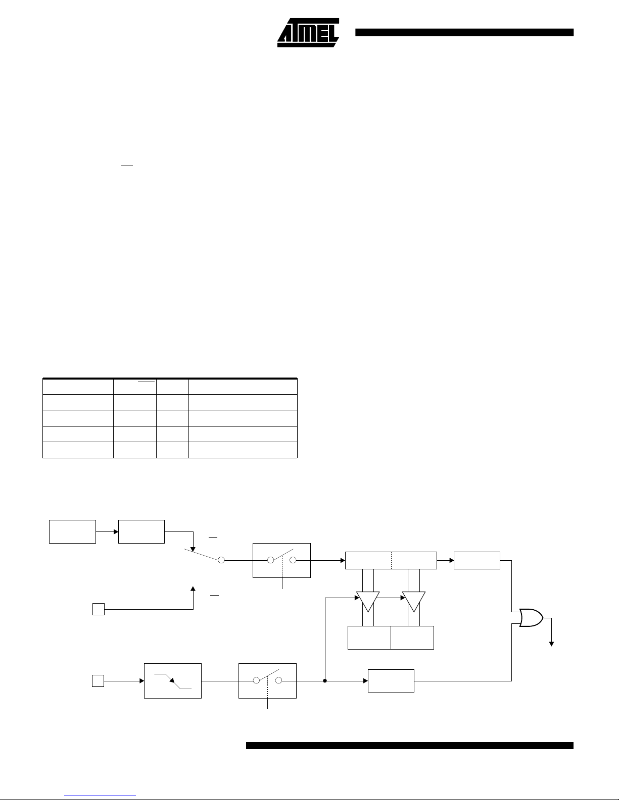
Timer 2
Timer 2 is a 16-bit Timer/Counter that can operate as
either a timer or an event counter. The type of operation is
selected by bit C/
2). Timer 2 has three operating modes: capture, auto-reload (up or down counting), and baud rate generator. The
modes are selected by bits in T2CON, as shown in Table
3.
Timer 2 consists of two 8-bit registers, TH2 and TL2. In the
Timer function, the TL2 register is incremented every machine cycle. Since a machine cycle consists of 12 oscillator periods, the count rate is 1/12 of the oscillator frequency.
In the Counter function, the register is incremented in response to a l-to-0 transition at its corresponding external
input pin, T2. In this function, the external input is sampled
during S5P2 of every machine cycle. When the samples
Table 3. Timer 2 Operating Modes
RCLK + TCLK CP/RL2 TR2 MODE
0 0 1 16-Bit Auto-Reload
0 1 1 16-Bit Capture
1 X 1 Bau d Rate Generator
X X 0 (Off)
T2 in the SFR T2CON (shown in Table
show a high in one cycle and a low in the next cy cle, the
count is incremented. The new count value appears in the
register during S3P1 of the cycle following the one in
which the transition was detected. Since two machine cycles (24 oscillator periods) are required to recognize a 1to-0 transition, the maximum count rate is 1/24 of the oscillator frequency. To ensure that a given level is sampled
at least once before it changes, the level should be held
for at least one full machine cycle.
Capture Mode
In the capture mode, two options are selected by bit
EXEN2 in T2CON. If EXEN2 = 0, Timer 2 is a 16-bit timer
or counter which upon overflow sets bit TF2 in T2CON.
This bit can then be used to generate an interrupt. If
EXEN2 = 1, Timer 2 performs the same operation, but a
l-to-0 transition at external input T2EX also cause s the
current value in TH2 and TL2 to be captured into RCAP2H
and RCAP2L, respectively. In addition, the transition at
T2EX causes bit EXF2 in T2CON to be set. T he E XF2 bit,
like TF2, can generate an interrupt. The capture mode is
illustrated in Figure 1.
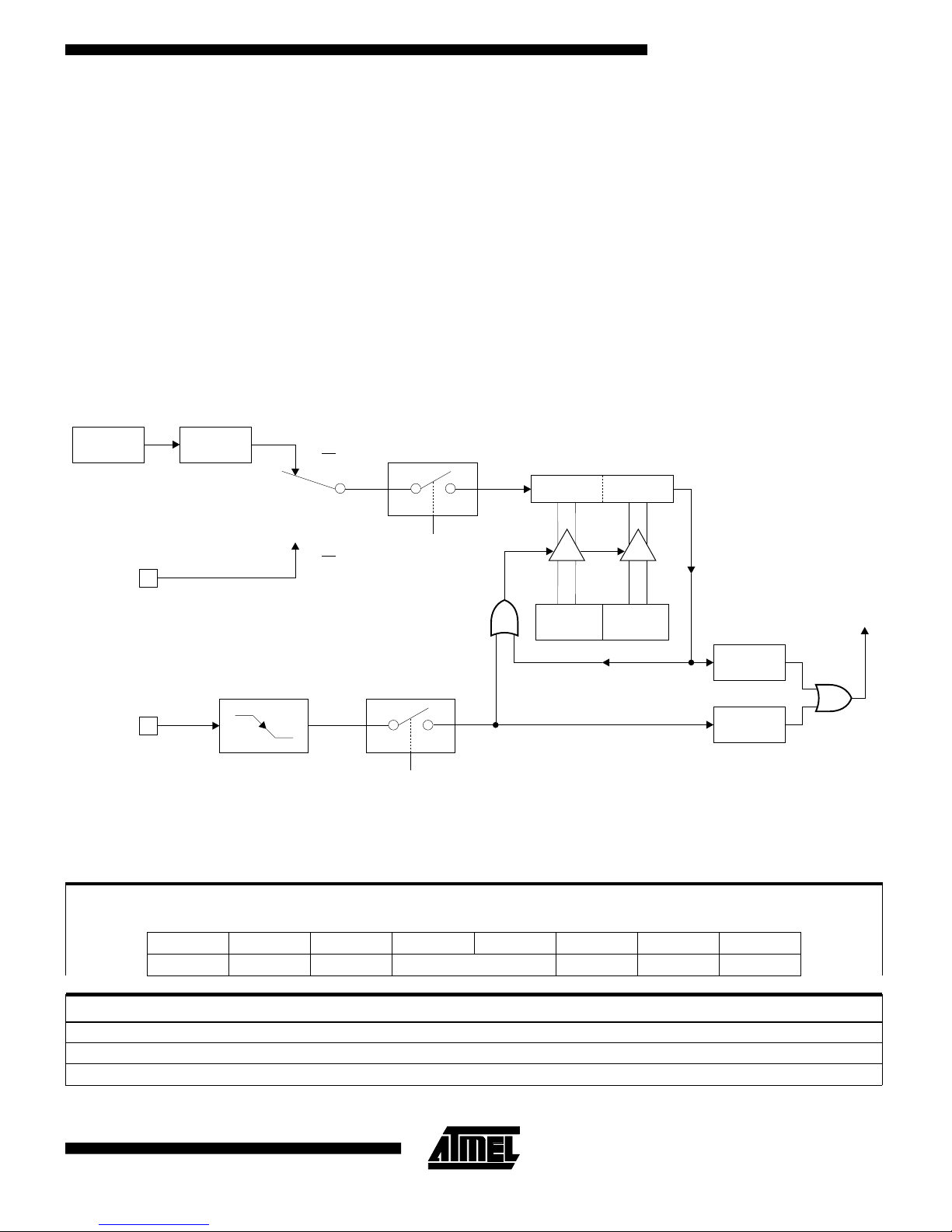
Auto-Reload (Up or Down Counter)
Timer 2 can be programmed to count up or down when
configured in its 16-bit auto-reload mode. This feature is
invoked by the DCEN (Down Counter Enable) bit located
in the SFR T2MOD (see Table 4). Upon reset, the DCEN
bit is set to 0 so that timer 2 will default to count up. When
DCEN is set, Timer 2 can count up or down, depending on
the value of the T2EX pin.
Figure 2 shows Timer 2 automatically counting up when
DCEN = 0. In this mode, two options are selected by bit
EXEN2 in T2CON. If EXEN2 = 0, Timer 2 counts up to
0FFFFH and then sets the TF2 bit upon overflow. The
Figure 1. Timer 2 in Capture Mode
OSC
T2 PIN
T2EX PIN
÷12
C/T2 = 0
C/T2 = 1
TRANSITION
DETECTOR
6 AT89C52
EXEN2
CONTROL
TR2
CAPTURE
CONTROL
TH2 TL2
RCAP2LRCAP2H
EXF2
TH2
OVERFLOW
TIMER 2
INTERRUPT
Page 7
Auto-Reload (Up or Down Counter) ( Continued)
overflow also causes the timer registers to be reloaded
with the 16-bit value in RCAP2H and RCAP2L. The values
in RCAP2H and RCAP2L are preset by software. If
EXEN2 = 1, a 16-bit reload can be triggered either by an
overflow or by a l-to-0 transition at external input T2EX.
This transition also sets the EXF2 bit. Both the TF2 and
EXF2 bits can generate an interrupt if enabled.
Setting the DCEN bit enables Timer 2 to count up or down,
as shown in Figure 3. In this mode, the T2EX pin controls
the direction of the count. A logic 1 at T2EX makes Timer
2 count up. The timer will overflow at 0FFFFH and set the
TF2 bit. This overflow also causes the 16-bit value in
Figure 2. Timer 2 Auto Reload Mode (DCEN = 0)
AT89C52
RCAP2H and RCAP2L to be reloaded into the timer registers, TH2 and TL2, respectively.
A logic 0 at T2EX makes Timer 2 count down. The timer
underflows when TH2 and TL2 equal the values stored in
RCAP2H and RCAP2L. The underflow sets the TF2 bit
and causes 0FFFFH to be reloaded into the timer registers.
The EXF2 bit toggles whenever Timer 2 overflows or underflows and can be used as a 17th bit of resolution. In this
operating mode, EXF2 does not flag an interrupt.
OSC
T2 PIN
T2EX PIN
÷12
C/T2 = 0
C/T2 = 1
TRANSITION
DETECTOR
EXEN2
Table 4. T2MOD—Timer 2 Mode Control Register
CONTROL
TR2
RELOAD
CONTROL
TH2 TL2
RCAP2LRCAP2H
OVERFLOW
TIMER 2
INTERRUPT
TF2
EXF2
T2MOD Address = 0C9H Reset Value = XXXX XX00B
Not Bit Addressable
——————T2OEDCEN
Bit76543210
Symbol Function
— Not implemented, reserved for future use.
T2OE Timer 2 Output Enable bit.
DCEN When set, this bit allows Timer 2 to be config ure d as an up/d own cou nt er.
7
Page 8

Figure 3. Timer 2 Auto Reload Mode (DCEN = 1)
OSC
12
÷
T2 PIN
C/T2 = 0
CONTROL
TR2
C/T2 = 1
Figure 4. Timer 2 in Baud Rate Generator Mode
(DOWN COUNTING RELOAD VALUE)
0FFH0FFH
OVERFLOW
TH2 TL2
RCAP2LRCAP2H
(UP COUNTING RELOAD VALUE)
TOGGLE
EXF2
TF2
TIMER 2
INTERRUPT
COUNT
DIRECTION
1=UP
0=DOWN
T2EX PIN
TIMER 1 OVERFLOW
OSC
T2 PIN
T2EX PIN
2
÷
TRANSITION
DETECTOR
NOTE: OSC. FREQ. IS DIVIDED BY 2, NOT 12
C/T2 = 0
TH2 TL2
CONTROL
TR2
C/T2 = 1
EXF2
CONTROL
EXEN2
2
÷
"0"
"1"
"0"
"1"
"0"
RCAP2LRCAP2H
TIMER 2
INTERRUPT
"1"
SMOD1
RCLK
6
÷
TCLK
16
÷
Rx
CLOCK
Tx
CLOCK
8 AT89C52
Page 9

AT89C52
Baud Rate Generator
Timer 2 is selected as the baud rate generator by setting
TCLK and/or RC LK in T2CON (Tabl e 2). Note that the
baud rates for transmit and receive can be different if
Timer 2 is used for the receiver or transmitter and Timer 1
is used for the other function. Setting RCLK and/or TCLK
puts Timer 2 into its baud rate generator mode, as shown
in Figure 4.
The baud rate generator mode is similar to the auto-reload
mode, in that a rollover in TH2 causes the Timer 2 registers to be reloaded with the 16-bit value in registers
RCAP2H and RCAP2L, which are preset by software.
The baud rates in Modes l and 3 are determined by Timer
2’s overflow rate according to the following equation.
Modes 1 and 3 Baud Rates =
The Timer can be configured for either timer or counter
operation. In most applications, it is configured for timer
operation (CP/
T2 = 0). The timer operation is different for
Timer 2 when it is used as a baud rate generator. Normally, as a timer, it increments every machine cycle (at
1/12 the oscillator frequency). As a baud rate generator,
Timer 2 Overflow Rate
16
however, it increments every state time (at 1/2 the oscillator frequency). The baud rate formula is given below.
Modes 1 and 3
Baud Rate
=
32 x
Oscillator Frequency
[65536 − (RCAP2H, RCAP2L)]
where (RCAP2H, RCAP2L) is the content of RCAP2H and
RCAP2L taken as a 16-bit unsigned integer.
Timer 2 as a baud rate generator is shown in Figure 4.
This figure is valid only if RCLK or TCLK = 1 in T2CON.
Note that a rollover in TH2 does not set TF2 and will not
generate an interrupt. Note too, that if EXEN2 is set, a l-to0 transition in T2EX will set EXF2 but will not cause a reload from (RCAP2H, RCAP2L) to (TH2, TL2). Thus when
Timer 2 is in use as a baud rate generator, T2EX can be
used as an extra external interrupt.
Note that when Timer 2 is running (TR2 = 1) as a timer in
the baud rate generator mode, TH2 or TL2 should not be
read from or written to. Under these conditions, the Timer
is incremented every state time, and the results of a read
or write may not be accurate. The RCAP2 registers may
be read but should not be written to, because a write might
overlap a reload and cause write and/or reload errors. The
timer should be turned off (clear TR2) before accessing
the Timer 2 or RCAP2 registers.
Figure 5. Timer 2 in Clock-Out Mode
OSC
P1.0
(T2)
TRANSITION
DETECTOR
P1.1
(T2EX)
÷2
TR2
C/T2 BIT
EXF2
÷2
TL2
(8-BITS)
RCAP2L RCAP2H
TIMER 2
INTERRUPT
TH2
(8-BITS)
T2OE (T2MOD.1)
EXEN2
9
Page 10

Programmable Clock Out
A 50% duty cycle clock can be programmed to come out
on P1.0, as shown in Figure 5. This pin, besides being a
regular I/0 pin, has two alternate functions. It can be programmed to input the external clock for Timer/Counter 2 or
to output a 50% duty cycle clock ranging from 61 Hz to 4
MHz at a 16
MHz operating frequency.
To configure the Timer/Counter 2 as a clock generator, bit
T2 (T2CON.1) must be cle ared and bit T2OE
C/
(T2MOD.1) must be set. Bit TR2 (T2CON.2) starts and
stops the timer.
The clock-out frequency depends on the oscillator frequency and the reload value of Timer 2 capture registers
(RCAP2H, RCAP2L), as shown in the following equation.
Clock−Out Frequency =
Oscillator Frequency
4 x [65536 − (RCAP2H, RCAP2L)]
In the clock-out mode, Timer 2 roll-overs will not generate
an interrupt. This behavior is similar to when Timer 2 is
used as a baud-rate generator. It is possible to use Timer
2 as a baud-rate generator and a clock generator simultaneously. Note, however, that the baud-rate and clock-out
frequencies cannot be determined independently from
one another since they both use RCAP2H and RCAP2L.
UART
The UART in the AT89C52 operates the same way as the
UART in the AT89C51.
Interrupts
The AT89C52 has a total of six interrupt vectors: two external interrupts (
(Timers 0, 1, and 2), and the serial port interrupt. These
interrupts are all shown in Figure 6.
Each of these interrupt sources can be individually enabled or disabl ed by setting or clearing a bit in Special
Function Register IE. IE also contains a global disable bit,
EA, which disables all interrupts at once.
Note that Table 5 shows that bit position IE.6 is unimplemented. In the AT89C51, bit position IE.5 is also unimplemented. User software should not write 1s to thes e bit positions, since they may be used in future AT89 products.
Timer 2 interrupt is generated by the logical OR of bits TF2
and EXF2 in register T2CON. Neither of these flags is
cleared by hardware when the service routine is vectored
to. In fact, the service routine may have to determine
whether it was TF2 or EXF2 that generated the interrupt,
and that bit will have to be cleared in software.
INT0 and INT1), three timer interrupts
The Timer 0 and Timer 1 flags, TF0 and TFI, are set at
S5P2 of the cycle in which the timers overflow. The values
are then polled by the circuitry in the next cycle. However,
the Timer 2 flag, TF2, is set at S2P2 and is polled in the
same cycle in which the timer overflows.
Table 5. Interrupt Enable (IE) Register
(MSB) (LSB)
EA — ET2 ES ET1 EX1 ET0 EX0
Enable Bit = 1 enab les the interrupt.
Enable Bit = 0 disables the interrupt .
Symbol Position Function
Disables all interru pts. If EA = 0, no
EA IE.7
— IE.6 Reserved.
ET2 IE.5 Timer 2 interrupt enable bit .
ES IE.4 Serial Port interrupt enable bit.
ET1 IE.3 Timer 1 interrupt enable bit .
EX1 IE.2 External interrupt 1 en ab le bit.
ET0 IE.1 Timer 0 interrupt enable bit .
EX0 IE.0 External interrupt 0 en ab le bit.
User software should neve r write 1s to unimplemented bits,
because they may be used in future AT89 products.
interrupt is ackn owledged. If EA = 1,
each interrupt so urce is individuall y
enabled or disabled by setting or
clearing its enable bit.
Figure 6. Interrupt Sources
0
INT0
TF0
INT1
TF1
RI
1
0
1
TI
IE0
IE1
10 AT89C52
TF2
EXF2
Page 11

AT89C52
Oscillator Characteristics
XTAL1 and XTAL2 are the input and output, respectively,
of an inverting amplifier that can be configured for use as
an on-chip oscillator, as shown in Figure 7. Either a quartz
crystal or ceramic resonator may be used. To drive the
device from an external clock source, XTAL2 should be
left unconnected while XTAL1 is driven, as shown in Figure 8. There are no requirements on the duty cycle of the
external clock signal, since the input to the internal clocking circuitry is through a divide-by-two flip-flop, but minimum and maximum voltage high and low time specifications must be observed.
Idle Mode
In idle mode, the CPU puts itself to sleep while all the onchip peripherals remain active. The mode is invoked by
software. The content of the on-chip RAM and all the special functions registers remain unchanged during this
mode. The idle mode can be terminated by any enabled
interrupt or by a hardware reset.
Note that when idle mode is terminated by a hardware reset, the device normally resumes program execution from
where it left off, up to two machine cycles before the internal reset algorithm takes control. On-chip hardware inhibits access to internal RAM in this event, but access to the
port pins is not inhibited. To eliminate the possibility of an
unexpected write to a port pin when idle mode is terminated by a reset, the instruction following the one that invokes idle mode should not write to a port pin or to external
memory.
Power Down Mode
In the power down mode, the oscillator is stopped, and the
instruction that invokes power down is the last instruction
executed. The on-chip RAM and Special Function Registers retain their values until the power down mode is terminated. The only exit from power down is a hardware reset.
Reset redefines the SFRs but does not change the onchip RAM. The reset should not be activated before V
is restored to its normal operating level and must be held
active long enough to allow the oscillator to restart and
stabilize.
CC
Figure 7. Oscillator Connections
C2
XTAL2
C1
XTAL1
GND
Notes: C1, C2 = 30 pF ± 10 pF for Crystals
= 40 pF ± 10 pF for Cerami c Res on ators
Figure 8. External Clock Drive Configuration
NC
EXTERNAL
OSCILLATOR
SIGNAL
XTAL2
XTAL1
GND
Status of External P i ns Dur ing Idle and Power Down
Mode Program Memory ALE PSEN PORT0 PORT1 P ORT2 PORT3
Idle Internal 1 1 Data Data Data Data
Idle External 1 1 Float Data Address Data
Power Down Internal 0 0 Data Data Data Data
Power Down External 0 0 Float Data Data Data
11
Page 12

Program Memory Lock Bits
The AT89C52 has three lock bits that can be left unprogrammed (U) or can be programmed (P) to obtain the additional features listed in the following table.
When lock bit 1 is programmed, the logic level at the
pin is sampled and latched during reset. If the device is
EA
powered up without a reset, the latch initializes to a random value and holds that value until reset is activated. The
latched value of
at that pin in order for the device to function properly.
EA must agree with the current logic level
Lock Bit Protection Modes
Program Lock Bits
LB1 LB2 LB3 Protection Type
1 U U U No program lock features.
MOVC instructions executed from external program memory are disabled from
2PUU
3 P P U Same as mode 2, but verify is also disabled.
4 P P P Same as mode 3, but external execution is also disabled.
fetching code bytes from internal memory,
further programming of the Flash memory is disabled.
is sampled and latched on reset, and
EA
Programming the Fl ash
The AT89C52 is normally shipped with the on-chip Flash
memory array in the erased state (that is, contents = FFH)
and ready to be programmed. The programming interface
accepts either a high-voltage (12-volt) or a low-voltage
) program enable signal. The low voltage program-
(V
CC
ming mode provides a convenient way to program the
AT89C52 inside the user’s system, while the high-voltage
programming mode is compatible with conventional third
party Flash or EPROM programmers.
The AT89C52 is shipped with either the high-voltage or
low-voltage programming mode enabled. The respective
top-side marking and device signature codes are listed in
the following table.
VPP = 12 V V
AT89C52 AT89C52
Top-Side Mark
Signature
The AT89C52 code memory array is programmed byteby-byte in either programming mode.
xxxx xxxx-5
yyww yyww
(030H)=1EH (030H)=1EH
(031H)=52H (031H)=52H
(032H)=FFH (032H)=05H
To program any
PP
= 5 V
non-blank byte in the on-chip Flash Memory, the entire
memory must be erased using the Chip Erase Mode.
Programming Algorithm: Before programming the
AT89C52, the address, data and control signals should be
set up according to the Flash programming mode table
and Figures 9 and 10. To program the AT89C52, take the
following steps.
1. Input the desired memory location on the address
lines.
2. Input the appropriate data byte on the data lines.
3. Activate the correct combination of control signals.
4. Raise
ming mode.
5. Pulse ALE/
array or the lock bits. The byte-write cycle is self-timed and
typically takes no more than 1.5 ms. Repeat steps 1
through 5, changing the address and data for the entire
array or until the end of the object file is reached.
Data Polling: The AT89C52 features Data Polling to indicate the end of a write cycle. During a write cycle, an attempted read of the last byte written will result in the complement of the written data on PO.7. Once the write cycle
has been completed, true data is valid on all outputs, and
the next cycle may begin.
after a write cycle has been initiated.
Ready/
also be monitored by the RDY/
pulled low after ALE goes high during programming to indicate
ming is done to indicate READY.
Program Verify: If lock bits LB1 and LB2 have not been
programmed, the programmed code data can be read
back via the address and data lines for verification. The
lock bits cannot be verified directly. Verification of the lock
EA/VPP to 12 V for t he high-voltage program-
PROG once to program a byte in the Flash
Busy: The progress of byte programming can
BUSY. P3.4 is pulled high again when program-
Data Polling may begin any time
BSY output signal. P3.4 is
(continued)
12 AT89C52
Page 13

AT89C52
Programming the Fl ash (Continued)
bits is achieved by observing that their features are enabled.
Chip Erase: The entire Flash array is erased electrically
by using the proper combination of control signals and by
holding ALE/
ten with all 1s. The chip erase operation must be executed
before the code memory can be reprogrammed.
Reading the Signature Bytes: The signature bytes are
read by the same procedure as a normal verification of
locations 030 H, 031H, and 032H, except that P3.6 and
P3.7 must be pulled to a logic low. The values returned are
as follows.
(030H) = 1EH indicates manufactured by Atmel
(031H) = 52H indicates 89C52
(032H) = FFH indicates 12 V programming
(032H) = 05H indicates 5 V programming
PROG low for 10 ms. The code array is writ-
Flash Programming Modes
ALE/
Mode RST PSEN
PROG
Programming Interfa ce
Every code byte in the Flash array can be written, and the
entire array can be erased, by using the appropriate combination of control signals. The write operation cycle is
self-timed and once initiated, will automatically time itself
to completion.
All major programming vendors offer worldwide support
for the Atmel microcontroller series. Please contact your
local programming vendor for the appropriate software revision.
EA/
V
PP
P2.6 P2.7 P3.6 P3.7
Write Code Data H L H/12V
Read Code Data H L H H L L H H
Write Lock Bit - 1 H L H/12V HHHH
Bit - 2 H L H/12V H H L L
Bit - 3 H L H/12V H L H L
Chip Erase H L H/12V H L L L
Read Signature
Byte
Notes: 1. The signature byte at location 032H designates
whether V
enableprogramming.
= 12 V or VPP = 5 V should be used to
PP
HLH HLLLL
(2)
2. Chip Erase requires a 10 ms
(1)
LHHH
PROG pulse.
13
Page 14

Figure 9. Programming the Flash Memory
Figure 10. Verifying the Flash Memory
ADDR.
OOOOH/1FFFH
SEE FLASH
PROGRAMMING
MODES TABLE
4-24 MHz
A0 - A7
A8 - A12
AT89C52
V
P1
P2.0 - P2.4
P2.6
P2.7
P3.6
P3.7
XTAL 2 EA
XTAL 1
GND
CC
P0
ALE
RST
PSEN
+5V
PGM
DATA
PROG
V/V
IH PP
V
IH
ADDR.
OOOOH/1FFFH
SEE FLASH
PROGRAMMING
MODES TABLE
4-24 MHz
A0 - A7
A8 - A12
AT89C52
P1
P2.0 - P2.4
P2.6
P2.7
P3.6
P3.7
XTAL 2 EA
XTAL 1
GND
V
P0
ALE
RST
PSEN
CC
+5V
PGM DATA
(USE 10K
PULLUPS)
V
IH
V
IH
Flash Programm ing and V er if i ca ti on Cha rac te rist i cs
TA = 21°C to 27°C, VCC = 5.0 ± 10%
Symbol Parameter Min Max Units
(1)
V
PP
(1)
I
PP
1/t
CLCL
t
AVGL
t
GHAX
t
DVGL
t
GHDX
t
EHSH
t
SHGL
(1)
t
GHSL
t
GLGH
t
AVQV
t
ELQV
t
EHQV
t
GHBL
t
WC
Note: 1. Only used in 12-volt programming mode.
Programming Enable Voltage 11.5 12.5 V
Programming Enable Current 1.0 mA
Oscillator Frequency 4 24 MHz
Address Setup to PROG Low 48t
Address Hold After PROG 48t
Data Setup to PROG Low 48t
Data Hold After PROG 48t
P2.7 (ENABLE) High to V
PP
48t
CLCL
CLCL
CLCL
CLCL
CLCL
VPP Setup to PROG Low 10 µs
VPP Hold After PROG 10 µs
PROG Width 1 110 µs
Address to Data Valid 48t
ENABLE Low to Data Valid 48t
Data Float After ENABLE 0 48t
CLCL
CLCL
CLCL
PROG High to BUSY Low 1.0 µs
Byte Write Cycle Time 2.0 ms
14 AT89C52
Page 15

AT89C52
Flash Programming and Veri fica tion Wa veforms - High Voltage Mode
P1.0 - P1.7
P2.0 - P2.4
P3.0
PORT 0
ALE/PROG
EA/V
PP
P2.7
(ENABLE)
P3.4
(RDY/BSY)
t
AVGL
t
SHGL
PROGRAMMING
ADDRESS
DATA IN
V
t
EHSH
PP
t
DVGL
t
GLGH
t
GHBL
t
GHDX
t
t
ELQV
GHAX
t
GHSL
LOGIC 1
LOGIC 0
BUSY
t
WC
VERIFICATION
ADDRESS
t
AVQV
DATA OUT
READY
t
EHQZ
Flash Programming and Verification Waveform s - Low V ol tage Mode
P1.0 - P1.7
P2.0 - P2.4
P3.0
PORT 0
ALE/PROG
EA/V
PP
P2.7
(ENABLE)
P3.4
(RDY/BSY)
t
AVGL
t
SHGL
PROGRAMMING
ADDRESS
DATA IN
t
EHSH
t
DVGL
t
GLGH
t
GHBL
t
GHDX
t
GHAX
LOGIC 1
LOGIC 0
t
ELQV
BUSY
t
WC
VERIFICATION
ADDRESS
t
AVQV
DATA OUT
READY
t
EHQZ
15
Page 16

Absolute Maximum Ra ti ngs *
Operating Temperature...................-55°C to +125°C
Storage Temperature...................... -65°C to +150°C
Voltage on Any Pin
with Respect to Ground ................... -1.0 V to +7.0 V
mum Ratings” may cause permanent da ma ge to th e de vice .
This is a stress rating only and functional operation of the
device at these or any other conditions beyond those indicated in the operational sections of this specification is not
implied. Exposure to absolute maximu m rating conditio ns
for extended periods may affect device reliability.
Maximum Operating Voltage ............................6.6 V
DC Output Current.......................................15.0 mA
D.C. Characteristics
The values shown in this table are valid for TA = -40°C to 85°C and VCC = 5.0 V ± 20%, unless otherwise noted.
Symbol Parameter Condition Min Max Units
*NOTICE: Stresses beyond those listed unde r “Absolu te Maxi-
V
IL
V
IL1
V
IH
V
IH1
V
OL
V
OL1
V
OH
V
OH1
I
IL
I
TL
I
LI
RRST Reset Pulldown Resistor 50 300 KΩ
C
IO
I
CC
Input Low Voltage (Except EA) -0.5 0.2 VCC-0.1 V
Input Low Voltage (EA)
-0.5 0.2 V
-0.3 V
CC
Input High Volta ge (Except XTAL1, RST) 0.2 VCC+0.9 VCC+0.5 V
Input High Volta ge
Output Low Voltage
(1)
(Ports 1,2,3)
Output Low Voltage
(1)
(Port 0, ALE, PSEN)
Output High Volta ge
(Ports 1,2,3, ALE,
PSEN)
Output High Volta ge
(Port 0 in External Bus Mode )
Logical 0 Input Current
(Ports 1,2,3)
Logical 1 to 0 Transition
Current (Ports 1,2,3)
Input Leakage Curre nt
(Port 0,
EA)
Pin Capacitance
Power Supply Current
Power Down Mode
(2)
(XTAL1, RST) 0.7 V
CC
IOL = 1.6 mA 0.45 V
IOL = 3.2 mA 0.45 V
I
= -60 µA, VCC = 5 V ± 10% 2.4 V
OH
IOH = -25 µA 0.75 V
IOH = -10 µA 0.9 V
CC
CC
IOH = -800 µA, VCC = 5 V ± 10% 2.4 V
IOH = -300 µA 0.75 V
IOH = -80 µA 0.9 V
= 0.45 V -50 µA
V
IN
= 2 V -650 µA
V
IN
0.45 < VIN < V
Test Freq. = 1 MHz , T
CC
= 25°C 10 pF
A
CC
CC
Active Mode, 12 MHz 25 mA
Idle Mode, 12 MHz 6.5 mA
VCC = 6 V 100 µA
V
= 3 V 40 µA
CC
VCC+0.5 V
±10 µA
V
V
V
V
Notes: 1. Under steady state (non-transient) conditions, I
must be externally limited as follows:
Maximum I
Maximum I
per port pin:10 mA
OL
per 8-bit port:
OL
Port 0:26 mA
Ports 1,2, 3:15 mA
16 AT89C52
OL
Maximum total IOL for all output pins:71 mA
If IOL exceeds the test condition, VOL may exceed the
related specification. Pins are not guaranteed to sink
current greate r than the listed tes t co nd itions.
2. Minimum V
for Power Down is 2 V.
CC
Page 17

AT89C52
A.C. Characteristics
Under operating conditions, load capacitance for Port 0, ALE/PROG, and PSEN = 100 pF; load capacitance for all
other outputs = 80 pF.
External Program and Data Memory Characte ristics
12 MHz Oscillator Variable Oscillator
Symbol Parameter
1/t
CLCL
t
LHLL
t
AVLL
t
LLAX
t
LLIV
t
LLPL
t
PLPH
t
PLIV
t
PXIX
t
PXIZ
t
PXAV
t
AVIV
t
PLAZ
t
RLRH
t
WLWH
t
RLDV
t
RHDX
t
RHDZ
t
LLDV
t
AVDV
t
LLWL
t
AVWL
t
QVWX
t
QVWH
t
WHQX
t
RLAZ
t
WHLH
Oscillator Frequency 0 24
ALE Pulse Width 127 2t
Address Valid to ALE Low 28 t
Address Hold After ALE Low 48 t
ALE Low to Valid Instruction In 233 4t
ALE Low to PSEN Low 43 t
PSEN Pulse Width 205 3t
PSEN Low to Valid Instruction In 145 3t
Input Instruction Hold After PSEN 0 0
Input Instruction Float After PSEN 59 t
PSEN to Address Valid 75 t
Address to Valid Instruction In 312 5t
PSEN Low to Address Float 10 10
RD Pulse Width 400 6t
WR Pulse Width 400 6t
RD Low to Valid Data In 252 5t
Data Hold After RD 0 0
Data Float After RD 97 2t
ALE Low to Valid Data In 517 8t
Address to Valid Data In 585 9t
ALE Low to RD or WR Low 200 300 3t
Address to RD or WR Low 203 4t
Data Valid to WR Transition 23 t
Data Valid to WR High 433 7t
Data Hold After WR 33 t
RD Low to Address Float 0 0
RD or WR High to ALE High 43 123 t
Min Max Min Max
-40
CLCL
-13
CLCL
-20
CLCL
CLCL
-13
CLCL
-20
CLCL
CLCL
CLCL
-8
CLCL
CLCL
-100
CLCL
-100
CLCL
CLCL
CLCL
CLCL
CLCL
-50 3t
CLCL
CLCL
CLCL
CLCL
CLCL
CLCL
-75
-20
-120
-20
-20 t
CLCL
CLCL
-65
-45
-10
-55
-90
-28
-150
-165
+50
+25
Units
MHz
ns
ns
ns
ns
ns
ns
ns
ns
ns
ns
ns
ns
ns
ns
ns
ns
ns
ns
ns
ns
ns
ns
ns
ns
ns
ns
17
Page 18

External Program Memory Read Cycle
t
LHLL
ALE
t
AVLL
PSEN
t
PORT 0
PORT 2
t
LLPL
t
LLAX
A0 - A7 A0 - A7
t
AVIV
A8 - A15
PLAZ
t
LLIV
t
PLIV
t
PXIZ
t
PXIX
INSTR IN
t
PLPH
t
PXAV
A8 - A15
External Data Mem or y Read Cycle
t
LHLL
ALE
PSEN
RD
PORT 0
PORT 2
t
AVLL
A0 - A7 FROM RI OR DPL
t
AVWL
P2.0 - P2.7 OR A8 - A15 FROM DPH
t
AVDV
t
t
LLAX
LLWL
t
RLAZ
t
LLDV
t
WHLH
t
RLRH
t
RLDV
DATA IN INSTR IN
t
RHDZ
t
RHDX
A0 - A7 FROM PCL
A8 - A15 FROM PCH
18 AT89C52
Page 19

External Data Mem ory Cycle
t
LHLL
ALE
PSEN
t
LLWL
t
WLWH
t
WHLH
AT89C52
WR
PORT 0
PORT 2
t
AVLL
A0 - A7 FROM RI OR DPL
P2.0 - P2.7 OR A8 - A15 FROM DPH
t
AVWL
t
LLAX
t
QVWX
External Clock Dr iv e Waveforms
t
0.7 V
CC
CHCX
CC
0.45V
V - 0.5V
CC
0.2 V - 0.1V
t
t
QVWH
DATA OUT INSTR IN
t
CLCH
t
CLCX
WHQX
A0 - A7 FROM PCL
A8 - A15 FROM PCH
t
CHCX
t
CLCL
t
CHCL
External Clock Dr iv e
Symbol Parameter Min Max Units
1/t
CLCL
t
CLCL
t
CHCX
t
CLCX
t
CLCH
t
CHCL
Oscillator Frequency 0 24 MHz
Clock Period 41.6 ns
High Time 15 ns
Low Time 15 ns
Rise Time 20 ns
Fall Time 20 ns
19
Page 20

Serial Port Timing: Shift Register Mode Test Conditions
The values in this table are valid for VCC = 5.0 V ± 20% and Load Capacitance = 80 pF.
12 MHz Osc Variable Oscillator
Symbol Parameter
t
XLXL
t
QVXH
t
XHQX
t
XHDX
t
XHDV
Serial Port Clock Cycle Time 1.0 12t
Output Data Setup to Clock Rising Edge 700 10t
Output Data Hold After Clock Rising Edge 50 2t
Input Data Hold After Clock Rising Edge 0 0 ns
Clock Rising Edge to Input Data Valid 700 10t
Min Max Min Max
CLCL
CLCL
Shift Register Mode Timing Waveforms
CLCL
-133 ns
-33 ns
-133 ns
CLCL
Units
µs
INSTRUCTION
0
1
2
ALE
t
XLXL
CLOCK
t
WRITE TO SBUF
OUTPUT DATA
CLEAR RI
QVXH
0
t
XHDV
VALID VALIDVALID VALIDVALID VALIDVALID VALID
t
XHQX
1
INPUT DATA
AC Testing Input/Output Wavefor m s
V - 0.5V
CC
0.45V
0.2 V + 0.9V
CC
TEST POINTS
0.2 V - 0.1V
CC
(1)
3
t
XHDX
4
2
3
5
Float Waveforms
+ 0.1V
V
LOAD
V
LOAD
- 0.1V
V
LOAD
6
4
(1)
Timing Reference
5
Points
7
6
8
7
SET TI
SET RI
- 0.1V
V
OL
+ 0.1V
V
OL
Note: 1. AC Inputs during testing are driven at VCC - 0.5 V
for a logic 1 and 0.45 V for a logic 0. Timing measurements are made at VIH min. for a logic 1 and
max. for a logic 0.
V
IL
20 AT89C52
Note: 1. For timing purposes, a port pin is no longer floating
when a 100-mV change from load volt ag e oc cu rs. A
port pin begins to float when a 100-mV change from
the loaded V
OH/VOL
level occurs.
Page 21

Ordering Information
AT89C52
Speed
(MHz)
12 5 V ± 20% AT89C52-12AC 44A Commercial
16 5 V ± 20% AT89C52-16AC 44A Commercial
20 5 V ± 20% AT89C52-20AC 44A Commercial
Power
Supply
5 V ± 10% AT89C52-12DM 40D6 Military
Ordering Code Package Operation Range
AT89C52-12JC 44J (0°C to 70°C)
AT89C52-12PC 40P6
AT89C52-12QC 44Q
AT89C52-12AI 44A Industrial
AT89C52-12JI 44J (-40°C to 85°C)
AT89C52-12PI 40P6
AT89C52-12QI 44Q
AT89C52-12AA 44A Automotive
AT89C52-12JA 44J (-40°C to 125°C)
AT89C52-12PA 40P6
AT89C52-12QA 44Q
AT89C52-12LM 44L (-55°C to 125°C)
AT89C52-12DM/883 40D6 Military/883C
AT89C52-12LM/883 44L Class B, Fully Compliant
(-55°C to 125°C)
AT89C52-16JC 44J (0°C to 70°C)
AT89C52-16PC 40P6
AT89C52-16QC 44Q
AT89C52-16AI 44A Industrial
AT89C52-16JI 44J (-40°C to 85°C)
AT89C52-16PI 40P6
AT89C52-16QI 44Q
AT89C52-16AA 44A Automotive
AT89C52-16JA 44J (-40°C to 125°C)
AT89C52-16PA 40P6
AT89C52-16QA 44Q
AT89C52-20JC 44J (0°C to 70°C)
AT89C52-20PC 40P6
AT89C52-20QC 44Q
AT89C52-20AI 44A Industrial
AT89C52-20JI 44J (-40°C to 85°C)
AT89C52-20PI 40P6
AT89C52-20QI 44Q
21
Page 22

Ordering Information
Speed
(MHz)
Power
Supply
Ordering Code Package Operation Range
24 5 V ± 20% AT89C52-24AC 44A Commercial
AT89C52-24JC 44J (0°C to 70°C)
AT89C52-24PC 44P6
AT89C52-24QC 44Q
AT89C52-24AI 44A Industrial
AT89C52-24JI 44J (-40°C to 85°C)
AT89C52-24PI 44P6
AT89C52-24QI 44Q
44A 44 Lead, Thin Plastic Gull Wing Quad Flat pack (TQFP)
40D6 40 Lead, 0.6 00 " Wi de , Non -Wi nd owed, Ceramic Dual Inline Package (Cerdip)
44J 44 Lead, Plastic J-Leade d Chi p Carrier (PLCC)
44L 44 Pad, Non-Windowed, Ceramic Leadless Chip Carrier (LCC)
40P6 40 Lead, 0.600" Wide, Plastic Dual Inl ine Pac ka ge (PDI P)
44Q 44 Lead, Plastic Gull Wing Quad Flatpack (PQFP)
22 AT89C52
Package Type
 Loading...