

Page 1

BDTIC www.bdtic.com/ATMEL
Features
• 80C52 Compatible
– 8051 Instruction Compatible
– Six 8-bit I/O Ports (64 pins or 68 Pins Versions)
– Four 8-bit I/O Ports (44 Pins Version)
– Three 16-bit Timer/Counters
– 256 bytes Scratch Pad RAM
– 11 Interrupt Sources With 4 Priority Levels
• ISP (In-System Programming) Using Standard V
• Integrated Power Monitor (POR/PFD) to Supervise Internal Power Supply
• Boot ROM Contains Serial Loader for In-System Programming
• High-speed Architecture
– In Standard Mode:
40 MHz (Vcc 2.7V to 5.5V, Both Internal and External Code Execution)
60 MHz (Vcc 4.5V to 5.5V and Internal Code Execution Only)
– In X2 Mode (6 Clocks/Machine Cycle)
20 MHz (Vcc 2.7V to 5.5V, Both Internal and External Code Execution)
30 MHz (Vcc 4.5V to 5.5V and Internal Code Execution Only)
• 128K bytes On-chip Flash Program/Data Memory
– 128 bytes Page Write with auto-erase
– 100k Write Cycles
• On-chip 8192 bytes Expanded RAM (XRAM)
– Software Selectable Size (0, 256, 512, 768, 1024, 1792, 2048, 4096, 8192 bytes)
• Dual Data Pointer
• Extended stack pointer to 512 bytes
• Variable Length MOVX for Slow RAM/Peripherals
• Improved X2 Mode with Independant Selection for CPU and Each Peripheral
• Keyboard Interrupt Interface on Port 1
• SPI Interface (Master/Slave Mode)
• 8-bit Clock Prescaler
• Programmable Counter Array with:
– High Speed Output
– Compare/Capture
– Pulse Width Modulator
– Watchdog Timer Capabilities
• Asynchronous Port Reset
• Two Full Duplex Enhanced UART with Dedicated Internal Baud Rate Generator
• Low EMI (inhibit ALE)
• Hardware Watchdog Timer (One-time Enabled with Reset-Out), Power-Off Flag
• Power Control Modes: Idle Mode, Power-down Mode
• Power Supply: 2.7V to 5.5V
• Temperature Ranges: Industrial (-40 to +85°C)
• Packages: PLCC44, VQFP44
Power Supply
CC
8-bit Flash
Microcontroller
AT89C51RE2
Page 2

AT89C51RE2
Description
AT89C51RE2 is a high performance CMOS Flash version of the 80C51 CMOS single chip 8-bit
microcontroller. It contains a 128 Kbytes Flash memory block for program.
The 128 Kbytes Flash memory can be programmed either in parallel mode or in serial mode with
the ISP capability or with software. The programming voltage is internally generated from the
standard VCC pin.
The AT89C51RE2 retains all features of the Atmel 80C52 with 256 bytes of internal RAM, a 10source 4-level interrupt controller and three timer/counters.
In addition, the AT89C51RE2 has a Programmable Counter Array, an XRAM of 8192 bytes, a
Hardware Watchdog Timer, SPI and Keyboard, two serial channels that facilitates multiprocessor communication (EUART), a speed improvement mechanism (X2 mode) and an extended
stack mode that allows the stack to be extended in the lower 256 bytes of XRAM.
The fully static design of the AT89C51RE2 allows to reduce system power consumption by
bringing the clock frequency down to any value, even DC, without loss of data.
The AT89C51RE2 has 2 software-selectable modes of reduced activity and 8-bit clock prescaler
for further reduction in power consumption. In the Idle mode the CPU is frozen while the peripherals and the interrupt system are still operating. In the power-down mode the RAM is saved and
all other functions are inoperative.
The added features of the AT89C51RE2 make it more powerful for applications that need pulse
width modulation, high speed I/O and counting capabilities such as alarms, motor control,
corded phones, smart card readers.
Table 1. Memory Size and I/O pins
AT89C51RE2 Flash (bytes) XRAM (bytes) TOTAL RAM (bytes) I/O
PLCC44
VQFP44
128K 8192 8192 + 256 34
2
7663C–8051–05/08
Page 3
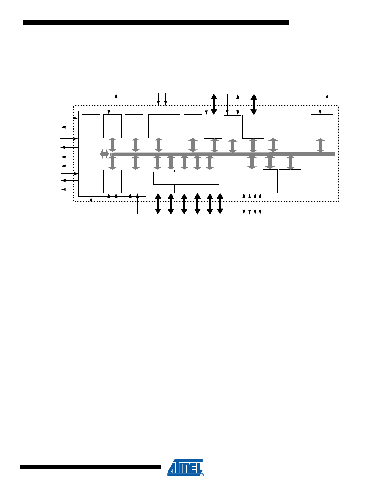
Block Diagram
Timer 0
INT
RAM
256x8
T0
T1
RxD_0
TxD_0
WR
RD
EA
PSEN
ALE/
XTALA2
XTALA1
EUART
CPU
Timer 1
INT1
Ctrl
INT0
(2)
(2)
C51
CORE
(2) (2) (2) (2)
Port 0P0Port 1
Port 2
Port 3
P1
P2
P3
XRAM
8192 x 8
IB-bus
PCA
RESET
PROG
Watch
Dog
PCA
ECI
Vss
VCC
(2)(2)
(1)
(1): Alternate function of Port 1
(2): Alternate function of Port 3
(1)
Timer2
T2EX
T2
(1) (1)
Flash
128Kx8
Keyboard
(1)
Keyboard
MISO
MOSI
SCK
SS
(3): Alternate function of Port 6
(3)
(3)
Port4
P4
(1)
(1)
(1)
(1)
BOOT
4K x8
ROM
Regulator
POR / PFD
Port 5
P5
Parallel I/O Ports &
External Bus
SPI
POR
PFD
XTALB2
XTALB1(1)
EUART_1
RxD_1
TxD_1
Figure 1. Block Diagram
AT89C51RE2
7663C–8051–05/08
3
Page 4
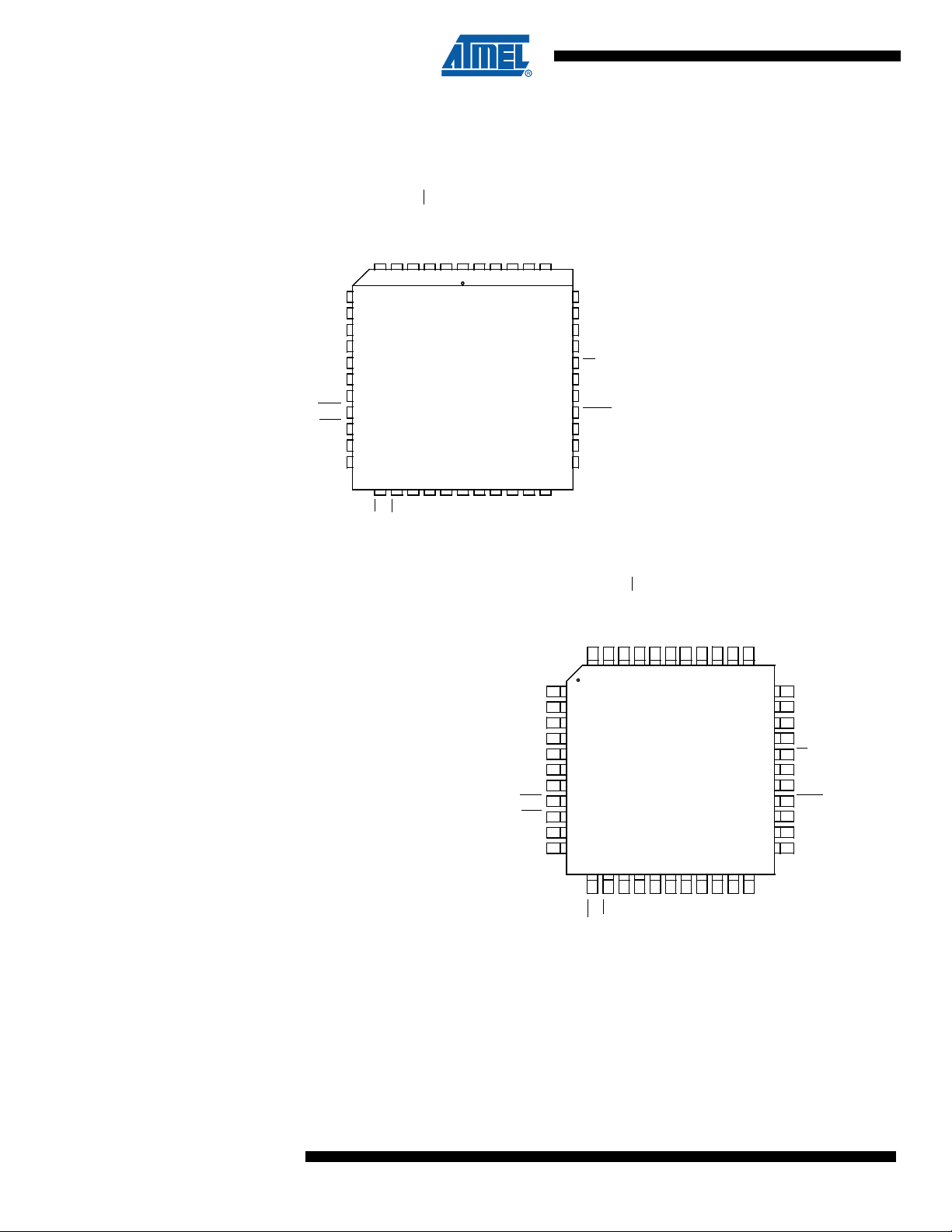
AT89C51RE2
Pin Configurations
43 42 41 40 3944
38 37 36 35 34
P1.4/CEX1
P1.0/T2/XTALB1
P1.1/T2EX/SS
P1.3/CEX0
P1.2/ECI
Rx_OCD
VCC
P0.0/AD0
P0.2/AD2
P0.3/AD3
P0.1/AD1
P0.4/AD4
P0.6/AD6
P0.5/AD5
P0.7/AD7
ALE
PSEN
EA
P6.1/TxD_1
P2.7/A15
P2.5/A13
P2.6/A14
P1.5/CEX2/MISO
P1.6/CEX3/SCK
P1.7/CEX4/MOSI
RST
P3.0/RxD_0
P6.0/RxD_1
P3.1/TxD_0
P3.2/INT0
P3.3/INT1
P3.4/T0
P3.5/T1
P3.6/WR
P3.7/RD
XTAL2
XTAL1
VSS
P2.0/A8
P2.1/A9
P2.2/A10
P2.3/A11
P2.4/A12
Tx_OCD
12 13 17161514 201918 21 22
33
32
31
30
29
28
27
26
25
24
23
1
2
3
4
5
6
7
8
9
10
11
VQFP44
PLCC44
AT89C51RE2
AT89C51RE2
P1.5/CEX2/MISO
P1.6/CEX3/SCK
P1.7/CEx4/MOSI
RST
P3.0/RxD_0
P6.0/RxD_1
P3.1/TxD_0
P3.2/INT0
P3.3/INT1
P3.4/T0
P3.5/T1
7
8
9
10
11
12
13
14
15
16
17
P1.4/CEX1
P1.3/CEX0
5 4 3 2 1 6
P1.0/T2
P1.1/T2EX/SS
P1.2/ECI
Rx_OCD
VCC
P0.0/AD0
44 43 42 41 40
18 19 23222120 262524 27 28
VSS
XTAL2
P3.7/RD
P3.6/WR
XTAL1
P2.0/A8
P2.1/A9
Tx_OCD
P0.3/AD3
P0.2/AD2
P0.1/AD1
39
P0.4/AD4
38
P0.5/AD5
37
P0.6/AD6
36
P0.7/AD7
35
EA
34
P6.1/TxD_1
33
ALE
32
PSEN
31
P2.7/A15
30
P2.6/A14
29
P2.5/A13
P2.2/A10
P2.3/A11
P2.4/A12
4
7663C–8051–05/08
Page 5

Table 2. Pin Description
Pin Number
AT89C51RE2
Mnemonic
V
SS
Vss1 39 I Optional Ground: Contact the Sales Office for ground connection.
V
CC
P0.0-P0.7 43-36 37-30 I/O Port 0: Port 0 is an open-drain, bidirectional I/O port. Port 0 pins that have 1s written to them
P1.0-P1.7 2-9 40-44
22 16 I Ground: 0V reference
44 38 I Power Supply: This is the power supply voltage for normal, idle and power-down operation
1-3
2 40 I/O T2 (P1.0): Timer/Counter 2 external count input/Clockout
3 41 I T2EX (P1.1): Timer/Counter 2 Reload/Capture/Direction Control
4 42 I ECI (P1.2): External Clock for the PCA
5 43 I/O CEX0 (P1.3): Capture/Compare External I/O for PCA module 0
Type Name and FunctionLCC VQFP 1.4
float and can be used as high impedance inputs. Port 0 must be polarized to VCC or VSS in
order to prevent any parasitic current consumption. Port 0 is also the multiplexed low-order
address and data bus during access to external program and data memory. In this
application, it uses strong internal pull-up when emitting 1s. Port 0 also inputs the code bytes
during EPROM programming. External pull-ups are required during program verification
during which P0 outputs the code bytes.
I/O Port 1: Port 1 is an 8-bit bidirectional I/O port with internal pull-ups. Port 1 pins that have 1s
written to them are pulled high by the internal pull-ups and can be used as inputs. As inputs,
Port 1 pins that are externally pulled low will source current because of the internal pull-ups.
Port 1 also receives the low-order address byte during memory programming and
verification.
Alternate functions for TSC8x54/58 Port 1 include:
6 44 I/O CEX1 (P1.4): Capture/Compare External I/O for PCA module 1
7 1 I/O CEX2 (P1.5): Capture/Compare External I/O for PCA module 2
8 2 I/O CEX3 (P1.6): Capture/Compare External I/O for PCA module 3
9 3 I/O CEX4 (P1.7): Capture/Compare External I/O for PCA module 4
P2.0-P2.7 24-31 18-25 I/O Port 2: Port 2 is an 8-bit bidirectional I/O port with internal pull-ups. Port 2 pins that have 1s
P3.0-P3.7 11,
13-19
11 5 I RXD_0 (P3.0): Serial input port
13 7 O TXD_0 (P3.1): Serial output port
5,
7-13
written to them are pulled high by the internal pull-ups and can be used as inputs. As inputs,
Port 2 pins that are externally pulled low will source current because of the internal pull-ups.
Port 2 emits the high-order address byte during fetches from external program memory and
during accesses to external data memory that use 16-bit addresses (MOVX @DPTR).In this
application, it uses strong internal pull-ups emitting 1s. During accesses to external data
memory that use 8-bit addresses (MOVX @Ri), port 2 emits the contents of the P2 SFR.
Some Port 2 pins receive the high order address bits during EPROM programming and
verification:
P2.0 to P2.5 for RB devices
P2.0 to P2.6 for RC devices
P2.0 to P2.7 for RD devices.
I/O Port 3: Port 3 is an 8-bit bidirectional I/O port with internal pull-ups. Port 3 pins that have 1s
written to them are pulled high by the internal pull-ups and can be used as inputs. As inputs,
Port 3 pins that are externally pulled low will source current because of the internal pull-ups.
Port 3 also serves the special features of the 80C51 family, as listed below.
7663C–8051–05/08
14 8 I INT0 (P3.2): External interrupt 0
5
Page 6
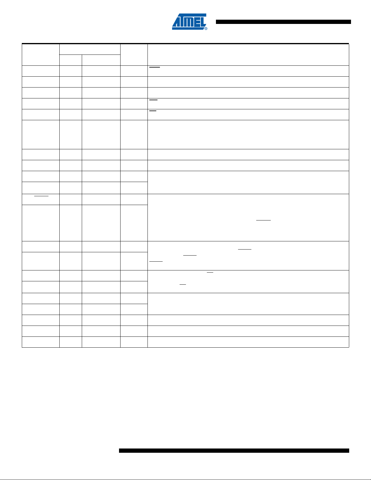
AT89C51RE2
Pin Number
Mnemonic
15 9 I INT1 (P3.3): External interrupt 1
16 10 I T0 (P3.4): Timer 0 external input
17 11 I T1 (P3.5): Timer 1 external input
18 12 O WR (P3.6): External data memory write strobe
19 13 O RD (P3.7): External data memory read strobe
P6.0-P6.1
Reset 10 4 I/O Reset: A high on this pin for two machine cycles while the oscillator is running, resets the
ALE/PROG 33 27 O (I) Address Latch Enable/Program Pulse: Output pulse for latching the low byte of the
12,34 6, 28
12 6 I RXD_1 (P6.0): Serial input port
34 28 O TXD_1 (P6.1): Serial output port
Type Name and FunctionLCC VQFP 1.4
Port 6: Port 6 is an 2-bit bidirectional I/O port with internal pull-ups. Port 6 pins that have 1s
written to them are pulled high by the internal pull-ups and can be used as inputs. As inputs,
Port 6 pins that are externally pulled low will source current because of the internal pull-ups.
Port 6 also serves some special features as listed below.
device. An internal diffused resistor to V
capacitor to VCC. This pin is an output when the hardware watchdog forces a system reset.
address during an access to external memory. In normal operation, ALE is emitted at a
constant rate of 1/6 (1/3 in X2 mode) the oscillator frequency, and can be used for external
timing or clocking. Note that one ALE pulse is skipped during each access to external data
memory. This pin is also the program pulse input (PROG) during Flash programming. ALE
can be disabled by setting SFR’s AUXR.0 bit. With this bit set, ALE will be inactive during
internal fetches.
permits a power-on reset using only an external
SS
PSEN 32 26 O Program Store ENable: The read strobe to external program memory. When executing
EA 35 29 I External Access Enable: EA must be externally held low to enable the device to fetch code
XTAL1 21 15 I
XTAL2 20 14 O Crystal 2: Output from the inverting oscillator amplifier
Tx_OCD 23 17 O Tx_OCD: On chip debug Serial output port
Rx_OCD 1 39 I Rx_OCD: On chip debug Serial input port
code from the external program memory, PSEN is activated twice each machine cycle,
except that two PSEN activations are skipped during each access to external data memory.
PSEN is not activated during fetches from internal program memory.
from external program memory locations 0000H to FFFFH (RD). If security level 1 is
programmed, EA will be internally latched on Reset.
Crystal 1: Input to the inverting oscillator amplifier and input to the internal clock generator
circuits.
6
7663C–8051–05/08
Page 7

AT89C51RE2
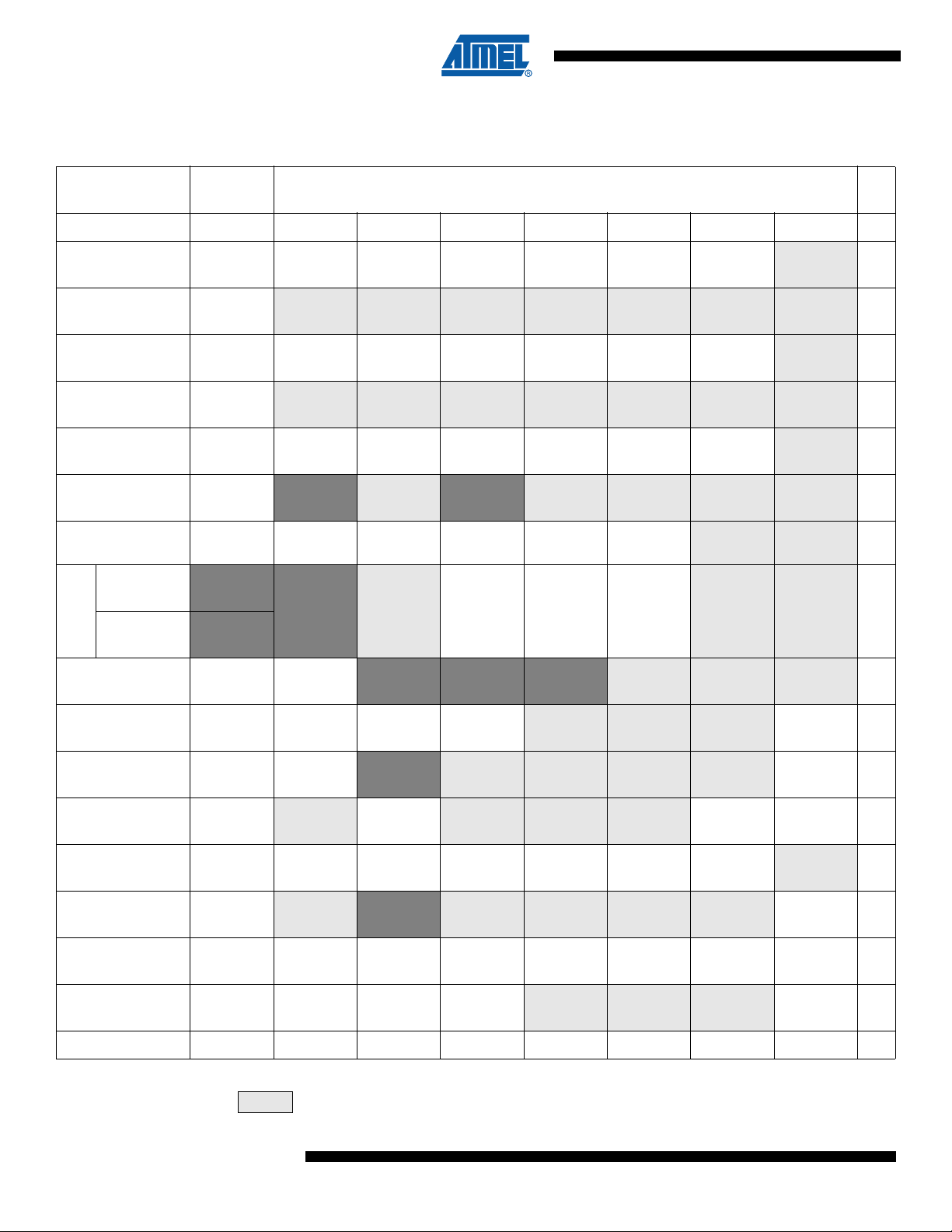
SFR Mapping
The Special Function Registers (SFRs) of the AT89C51RE2 fall into the following categories:
• C51 core registers: ACC, B, DPH, DPL, PSW, SP
• I/O port registers: P0, P1, P2, P3, P4, P5, P6
• Timer registers: T2CON, T2MOD, TCON, TH0, TH1, TH2, TMOD, TL0, TL1, TL2, RCAP2L,
RCAP2H
• Serial I/O port registers: SADDR_0, SADEN_0, SBUF_0, SCON_0, SADDR_1, SADEN_1,
SBUF_1, SCON_1,
• PCA (Programmable Counter Array) registers: CCON, CCAPMx, CL, CH, CCAPxH,
CCAPxL (x: 0 to 4)
• Power and clock control registers: PCON, CKAL, CKCON0_1
• Hardware Watchdog Timer registers: WDTRST, WDTPRG
• Interrupt system registers: IE0, IPL0, IPH0, IE1, IPL1, IPH1
• Keyboard Interface registers: KBE, KBF, KBLS
• SPI registers: SPCON, SPSTR, SPDAT
• BRG (Baud Rate Generator) registers: BRL_0, BRL_1, BDRCON_0, BDRCON_1
• Memory register: FCON, FSTA
• Clock Prescaler register: CKRL
• Others: AUXR, AUXR1, CKCON0, CKCON1, BMSEL
7663C–8051–05/08
7
Page 8

AT89C51RE2
Table 3. C51 Core SFRs
Mnemonic Add Name 7 6 5 4 3 2 1 0
ACC E0h Accumulator
B F0h B Register
PSW D0h Program Status Word CY AC F0 RS1 RS0 OV F1 P
SP 81h Stack Pointer
DPL 82h Data Pointer Low byte
DPH 83h Data Pointer High byte
Table 4. System Management SFRs
Mnemonic Add Name 7 6 5 4 3 2 1 0
PCON 87h Power Control
AUXR 8Eh Auxiliary Register 0 - - M0 XRS2 XRS1 XRS0
AUXR1 A2h Auxiliary Register 1 EES SP9 U2 - GF2 0 - DPS
CKRL 97h Clock Reload Register - - - - - - - -
BMSEL 92h Bank Memory Select MBO2 MBO1 MBO0 - FBS2 FBS1 FBS0
CKCON0 8Fh Clock Control Register 0 - WDX2 PCAX2 SIX2_0 T2X2 T1X2 T0X2 X2
CKCON1 AFh Clock Control Register 1 - - - - - - SIX2_1 SPIX2
SMOD1_0 SMOD0_0
- POF GF1 GF0 PD IDL
EXTRA
M
AO
Table 5. Interrupt SFRs
Mnemonic Add Name 7 6 5 4 3 2 1 0
IEN0 A8h Interrupt Enable Control 0 EA EC ET2 ES ET1 EX1 ET0 EX0
IEN1 B1h Interrupt Enable Control 1 - - - - ES_1 ESPI ETWI EKBD
IPH0 B7h Interrupt Priority Control High 0 - PPCH PT2H PSH PT1H PX1H PT0H PX0H
IPL0 B8h Interrupt Priority Control Low 0 - PPCL PT2L PSL PT1L PX1L PT0L PX0L
IPH1 B3h Interrupt Priority Control High 1 - - - - PSH_1 SPIH IE2CH KBDH
IPL1 B2h Interrupt Priority Control Low 1 - - - - PSL_1 SPIL IE2CL KBDL
Table 6. Port SFRs
Mnemonic Add Name 7 6 5 4 3 2 1 0
P0 80h 8-bit Port 0
P1 90h 8-bit Port 1
P2 A0h 8-bit Port 2
P3 B0h 8-bit Port 3
P4 C0h 8-bit Port 4
8
7663C–8051–05/08
Page 9

AT89C51RE2
Table 6. Port SFRs
Mnemonic Add Name 7 6 5 4 3 2 1 0
P5 E8h 8-bit Port 5
P6 F8h 2-bit Port 5 - - - - - -
Table 7. Flash and EEPROM Data Memory SFR
Mnemonic Add Name 7 6 5 4 3 2 1 0
FCON D1h Flash Controller Control FPL3 FPL2 FPL1 FPL0 FPS FMOD2 FMOD1 FMOD0
FSTA D3h Flash Controller Status FMR FSE FLOAD FBUSY
Table 8. Timer SFRs
Mnemonic Add Name 7 6 5 4 3 2 1 0
TCON 88h Timer/Counter 0 and 1 Control TF1 TR1 TF0 TR0 IE1 IT1 IE0 IT0
TMOD 89h Timer/Counter 0 and 1 Modes GATE1 C/T1# M11 M01 GATE0 C/T0# M10 M00
TL0 8Ah Timer/Counter 0 Low Byte
TH0 8Ch Timer/Counter 0 High Byte
TL1 8Bh Timer/Counter 1 Low Byte
TH1 8Dh Timer/Counter 1 High Byte
WDTRST A6h WatchDog Timer Reset
WDTPRG A7h WatchDog Timer Program - - - - - WTO2 WTO1 WTO0
T2CON C8h Timer/Counter 2 control TF2 EXF2 RCLK TCLK EXEN2 TR2 C/T2# CP/RL2#
T2MOD C9h Timer/Counter 2 Mode - - - - - - T2OE DCEN
RCAP2H CBh
RCAP2L CAh
TH2 CDh Timer/Counter 2 High Byte
TL2 CCh Timer/Counter 2 Low Byte
Timer/Counter 2 Reload/Capture
High byte
Timer/Counter 2 Reload/Capture
Low byte
Table 9. PCA SFRs
Mnemo
-nic Add Name 7 6 5 4 3 2 1 0
CCON D8h PCA Timer/Counter Control CF CR - CCF4 CCF3 CCF2 CCF1 CCF0
CMOD D9h PCA Timer/Counter Mode CIDL WDTE - - - CPS1 CPS0 ECF
CL E9h PCA Timer/Counter Low byte
7663C–8051–05/08
9
Page 10

AT89C51RE2
Table 9. PCA SFRs (Continued)
Mnemo
-nic Add Name 7 6 5 4 3 2 1 0
CH F9h PCA Timer/Counter High byte
CCAPM0
CCAPM1
CCAPM2
CCAPM3
CCAPM4
CCAP0H
CCAP1H
CCAP2H
CCAP3H
CCAP4H
CCAP0L
CCAP1L
CCAP2L
CCAP3L
CCAP4L
DAh
PCA Timer/Counter Mode 0
DBh
PCA Timer/Counter Mode 1
DCh
PCA Timer/Counter Mode 2
DDh
PCA Timer/Counter Mode 3
DEh
PCA Timer/Counter Mode 4
FAh
PCA Compare Capture Module 0 H
FBh
PCA Compare Capture Module 1 H
FCh
PCA Compare Capture Module 2 H
FDh
PCA Compare Capture Module 3 H
FEh
PCA Compare Capture Module 4 H
EAh
PCA Compare Capture Module 0 L
EBh
PCA Compare Capture Module 1 L
ECh
PCA Compare Capture Module 2 L
EDh
PCA Compare Capture Module 3 L
EEh
PCA Compare Capture Module 4 L
-
CCAP0H7
CCAP1H7
CCAP2H7
CCAP3H7
CCAP4H7
CCAP0L7
CCAP1L7
CCAP2L7
CCAP3L7
CCAP4L7
ECOM0
ECOM1
ECOM2
ECOM3
ECOM4
CCAP0H6
CCAP1H6
CCAP2H6
CCAP3H6
CCAP4H6
CCAP0L6
CCAP1L6
CCAP2L6
CCAP3L6
CCAP4L6
CAPP0
CAPP1
CAPP2
CAPP3
CAPP4
CCAP0H5
CCAP1H5
CCAP2H5
CCAP3H5
CCAP4H5
CCAP0L5
CCAP1L5
CCAP2L5
CCAP3L5
CCAP4L5
CAPN0
CAPN1
CAPN2
CAPN3
CAPN4
CCAP0H4
CCAP1H4
CCAP2H4
CCAP3H4
CCAP4H4
CCAP0L4
CCAP1L4
CCAP2L4
CCAP3L4
CCAP4L4
MAT0
MAT1
MAT2
MAT3
MAT4
CCAP0H3
CCAP1H3
CCAP2H3
CCAP3H3
CCAP4H3
CCAP0L3
CCAP1L3
CCAP2L3
CCAP3L3
CCAP4L3
TOG0
TOG1
TOG2
TOG3
TOG4
CCAP0H2
CCAP1H2
CCAP2H2
CCAP3H2
CCAP4H2
CCAP0L2
CCAP1L2
CCAP2L2
CCAP3L2
CCAP4L2
PWM0
PWM1
PWM2
PWM3
PWM4
CCAP0H1
CCAP1H1
CCAP2H1
CCAP3H1
CCAP4H1
CCAP0L1
CCAP1L1
CCAP2L1
CCAP3L1
CCAP4L1
ECCF0
ECCF1
ECCF2
ECCF3
ECCF4
CCAP0H0
CCAP1H0
CCAP2H0
CCAP3H0
CCAP4H0
CCAP0L0
CCAP1L0
CCAP2L0
CCAP3L0
CCAP4L0
Table 10. Serial I/O Port SFRs
Mnemonic Add Name 7 6 5 4 3 2 1 0
SCON_0 98h Serial Control 0 FE/SM0_0 SM1_0 SM2_0 REN_0 TB8_0 RB8_0 TI_0 RI_0
SBUF_0 99h Serial Data Buffer 0
SADEN_0 B9h Slave Address Mask 0
SADDR_0 A9h Slave Address 0
BDRCON_0 9Bh Baud Rate Control 0 BRR_0 TBCK_0 RBCK_0 SPD_0 SRC_0
BRL_0 9Ah Baud Rate Reload 0
SCON_1 C0h Serial Control 1 FE_1/SM0_1 SM1_1 SM2_1 REN_1 TB8_1 RB8_1 TI_1 RI_1
SBUF_1 C1h Serial Data Buffer 1
SADEN_1 BAh Slave Address Mask 1
SADDR_1 AAh Slave Address 1
BDRCON_1 BCh Baud Rate Control 1 SMOD1_1 SMOD0_1 BRR_1 TBCK_1 RBCK_1 SPD_1 SRC_1
BRL_1 BBh Baud Rate Reload 1
10
7663C–8051–05/08
Page 11

AT89C51RE2
Table 11. SPI Controller SFRs
Mnemonic Add Name 7 6 5 4 3 2 1 0
SPCON C3h SPI Control SPR2 SPEN SSDIS MSTR CPOL CPHA SPR1 SPR0
SPSCR C4h SPI Status SPIF OVR MODF SPTE UARTM SPTEIE MODFIE
SPDAT C5h SPI Data SPD7 SPD6 SPD5 SPD4 SPD3 SPD2 SPD1 SPD0
Table 12. Keyboard Interface SFRs
Mnemonic Add Name 7 6 5 4 3 2 1 0
KBLS 9Ch Keyboard Level Selector KBLS7 KBLS6 KBLS5 KBLS4 KBLS3 KBLS2 KBLS1 KBLS0
KBE 9Dh Keyboard Input Enable KBE7 KBE6 KBE5 KBE4 KBE3 KBE2 KBE1 KBE0
KBF 9Eh Keyboard Flag Register KBF7 KBF6 KBF5 KBF4 KBF3 KBF2 KBF1 KBF0
7663C–8051–05/08
11
Page 12
AT89C51RE2
Table 13. SFR Mapping
addressable Non Bit addressable
Table below shows all SFRs with their address and their reset value.
Bit
0/8 1/9 2/A 3/B 4/C 5/D 6/E 7/F
C0h
F8h
F0h
E8h
E0h
D8h
D0h
C8h
U2(AUXR1.5)
=0
U2(AUXR1.5)
=1
B8h
P6
XXXX XX11CH0000 0000
B
0000 0000
P5
1111 1111CL0000 0000
ACC
0000 0000
CCON
00X0 0000
PSW
0000 0000
T2CON
0000 0000
SCON_1
0000 0000
P4
1111 1111
IPL0
X000 000
CMOD
00XX X000
FCON
0000 0000
T2MOD
XXXX XX00
SBUF_1
0000 0000
SADEN_0
0000 0000
CCAP0H
XXXX XXXX
CCAP0L
XXXX XXXX
CCAPM0
X000 0000
RCAP2L
0000 0000
SADEN1
0000 0000
CCAP1H
XXXX XXXX
CCAP1L
XXXX XXXX
CCAPM1
X000 0000
FSTA
xxxx x000
RCAP2H
0000 0000
SPCON
0001 0100
BRL_1
0000 0000
CCAP2H
XXXX XXXX
CCAP2L
XXXX XXXX
CCAPM2
X000 0000
TL2
0000 0000
SPSCR
0000 0000
BDRCON_1
XXX0 0000
CCAP3H
XXXX XXXX
CCAP3L
XXXX XXXX
CCAPM3
X000 0000
TH2
0000 0000
SPDAT
XXXX XXXX
CCAP4H
XXXX XXXX
CCAP4L
XXXX XXXX
CCAPM4
X000 0000
FFh
F7h
EFh
E7h
DFh
D7h
CFh
C7h
BFh
12
B0h
A8h
A0h
98h
90h
88h
80h
P3
1111 1111
IEN0
0000 0000
P2
1111 1111
SCON_0
0000 0000
P1
1111 1111
TCON
0000 0000
P0
1111 1111
0/8 1/9 2/A 3/B 4/C 5/D 6/E 7/F
IEN1
XXXX 0000
SADDR_0
0000 0000
SBUF_0
XXXX XXXX
TMOD
0000 0000
SP
0000 0111
IPL1
XXXX 0000
SADDR_1
0000 0000
AUXR1
000x 11x0
BRL_0
0000 0000
BMSEL
0000 0YYY
TL0
0000 0000
DPL
0000 0000
IPH1
XXXX 0111
BDRCON_0
XXX0 0000
TL1
0000 0000
DPH
0000 0000
KBLS
0000 0000
TH0
0000 0000
KBE
0000 0000
TH1
0000 0000
WDTRST
XXXX XXXX
KBF
0000 0000
AUXR
XX00 1000
Reserved
IPH0
X000 0000
CKCON1
XXXX XX00
WDTPRG
XXXX X000
CKRL
1111 1111
CKCON0
0000 0000
PCON
00X1 0000
7663C–8051–05/08
B7h
AFh
A7h
9Fh
97h
8Fh
87h
Page 13
AT89C51RE2
XTAL1
2
CKCON0
X2
8 bit Prescaler
F
OSC
FXTAL
0
1
XTAL1:2
F
CLK CPU
F
CLK PERIPH
CKRL
Enhanced Features
X2 Feature
In comparison to the original 80C52, the AT89C51RE2 implements some new features, which
are
:
• X2 option
• Dual Data Pointer
• Extended RAM
• Extended stack
• Programmable Counter Array (PCA)
• Hardware Watchdog
• SPI interface
• 4-level interrupt priority system
• power-off flag
• ONCE mode
• ALE disabling
• Enhanced features on the UART and the timer 2
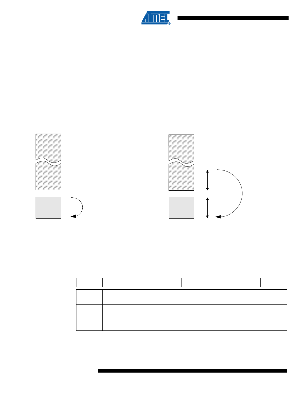
The AT89C51RE2 core needs only 6 clock periods per machine cycle. This feature called ‘X2’
provides the following advantages:
• Divide frequency crystals by 2 (cheaper crystals) while keeping same CPU power.
• Save power consumption while keeping same CPU power (oscillator power saving).
• Save power consumption by dividing dynamically the operating frequency by 2 in operating
and idle modes.
• Increase CPU power by 2 while keeping same crystal frequency.
In order to keep the original C51 compatibility, a divider by 2 is inserted between the XTAL1 signal and the main clock input of the core (phase generator). This divider may be disabled by
software.
Description The clock for the whole circuit and peripherals is first divided by two before being used by the
CPU core and the peripherals.
This allows any cyclic ratio to be accepted on XTAL1 input. In X2 mode, as this divider is
bypassed, the signals on XTAL1 must have a cyclic ratio between 40 to 60%.
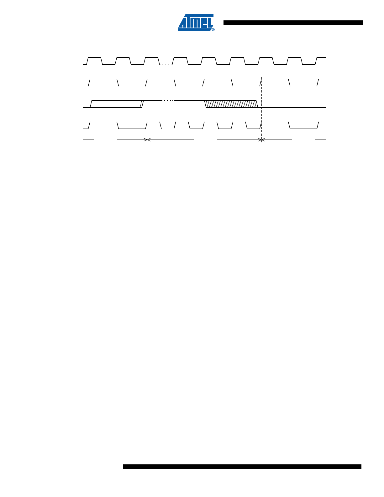
Figure 2 shows the clock generation block diagram. X2 bit is validated on the rising edge of the
XTAL1÷2 to avoid glitches when switching from X2 to STD mode. Figure 3 shows the switching
mode waveforms.
Figure 2. Clock Generation Diagram
7663C–8051–05/08
13
Page 14
AT89C51RE2
Figure 3. Mode Switching Waveforms
XTAL1:2
XTAL1
CPU clock
X2 bit
X2 ModeSTD Mode STD Mode
F
OSC
The X2 bit in the CKCON0 register (see Table 14) allows a switch from 12 clock periods per
instruction to 6 clock periods and vice versa. At reset, the speed is set according to X2 bit of the
Fuse Configuration Byte (FCB). By default, Standard mode is active. Setting the X2 bit activates
the X2 feature (X2 mode).
The T0X2, T1X2, T2X2, UartX2, PcaX2, and WdX2 bits in the CKCON0 register (See Table 14.)
and SPIX2 bit in the CKCON1 register (see Table 15) allows a switch from standard peripheral
speed (12 clock periods per peripheral clock cycle) to fast peripheral speed (6 clock periods per
peripheral clock cycle). These bits are active only in X2 mode.
14
7663C–8051–05/08
Page 15

AT89C51RE2
Table 14. CKCON0 Register
CKCON0 - Clock Control Register (8Fh)
7 6 5 4 3 2 1 0
- WDX2 PCAX2 SIX2_0 T2X2 T1X2 T0X2 X2
Bit
Number
7 - Reserved
6 WDX2
5 PCAX2
4 SIX2_0
3 T2X2
Bit
Mnemonic Description
Watchdog Clock
(This control bit is validated when the CPU clock X2 is set; when X2 is low, this bit has no
effect).
Cleared to select 6 clock periods per peripheral clock cycle.
Set to select 12 clock periods per peripheral clock cycle.
Programmable Counter Array Clock
(This control bit is validated when the CPU clock X2 is set; when X2 is low, this bit has no
effect).
Cleared to select 6 clock periods per peripheral clock cycle. Set to select 12 clock
periods per peripheral clock cycle.
Enhanced UART0 Clock (Mode 0 and 2)
(This control bit is validated when the CPU clock X2 is set; when X2 is low, this bit has no
effect).
Cleared to select 6 clock periods per peripheral clock cycle. Set to select 12 clock
periods per peripheral clock cycle.
Timer2 Clock
(This control bit is validated when the CPU clock X2 is set; when X2 is low, this bit has no
effect).
Cleared to select 6 clock periods per peripheral clock cycle.
Set to select 12 clock periods per peripheral clock cycle.
7663C–8051–05/08
Timer1 Clock
2 T1X2
1 T0X2
0 X2
(This control bit is validated when the CPU clock X2 is set; when X2 is low, this bit has no
effect).
Cleared to select 6 clock periods per peripheral clock cycle. Set to select 12 clock
periods per peripheral clock cycle.
Timer0 Clock
(This control bit is validated when the CPU clock X2 is set; when X2 is low, this bit has no
effect).
Cleared to select 6 clock periods per peripheral clock cycle. Set to select 12 clock
periods per peripheral clock cycle.
CPU Clock
Cleared to select 12 clock periods per machine cycle (STD mode) for CPU and all the
peripherals. Set to select 6clock periods per machine cycle (X2 mode) and to enable the
individual peripherals’X2’ bits. Programmed by hardware after Power-up regarding
Hardware Security Byte (HSB), Default setting, X2 is cleared.
Reset Value = X000 000’HSB. X2’b (See “Fuse Configuration Byte: FCB”)
Not bit addressable
15
Page 16

AT89C51RE2
Table 15. CKCON1 Register
CKCON1 - Clock Control Register (AFh)
7 6 5 4 3 2 1 0
- - - - - - SIX2_1 SPIX2
Bit
Number
7 - Reserved
6 - Reserved
5 - Reserved
4 - Reserved
3 - Reserved
2 - Reserved
1 SIX2_1
0 SPIX2
Bit
Mnemonic Description
Enhanced UART1 Clock (Mode 0 and 2)
(This control bit is validated when the CPU clock X2 is set; when X2 is low, this bit has no
effect).
Cleared to select 6 clock periods per peripheral clock cycle. Set to select 12 clock
periods per peripheral clock cycle.
SPI (This control bit is validated when the CPU clock X2 is set; when X2 is low, this bit
has no effect).
Clear to select 6 clock periods per peripheral clock cycle.
Set to select 12 clock periods per peripheral clock cycle.
Reset Value = XXXX XX00b
Not bit addressable
16
7663C–8051–05/08
Page 17
AT89C51RE2
External Data Memory
AUXR1(A2H)
DPS
DPH(83H) DPL(82H)
07
DPTR0
DPTR1
Dual Data Pointer Register DPTR
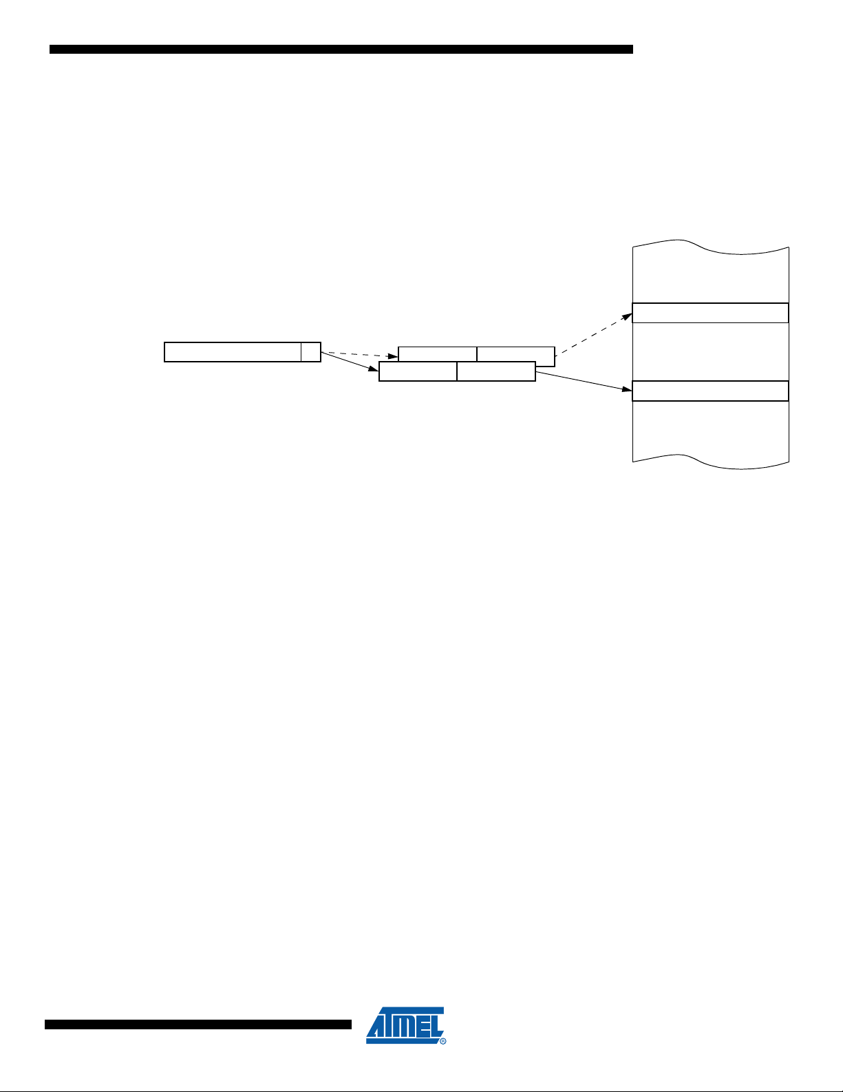
Figure 4. Use of Dual Pointer
The additional data pointer can be used to speed up code execution and reduce code size.
The dual DPTR structure is a way by which the chip will specify the address of an external data
memory location. There are two 16-bit DPTR registers that address the external memory, and a
single bit called DPS = AUXR1.0 (see Table 16) that allows the program code to switch between
them (Refer to Figure 4).
7663C–8051–05/08
17
Page 18

AT89C51RE2
Table 16. AUXR1 register
AUXR1- Auxiliary Register 1(0A2h)
7 6 5 4 3 2 1 0
EES SP9 U2 - GF2 0 - DPS
Bit
Number
7 EES
6 SP9
5 U2
4 -
3 GF2 This bit is a general purpose user flag. *
2 0 Always cleared.
1 -
0 DPS
Bit
Mnemonic Description
Enable Extended Stack
This bit allows the selection of the stack extended mode.
Set to enable the extended stack
Clear to disable the extended stack (default value)
Stack Pointer 9th Bit
This bit has no effect when the EES bit is cleared.
Set when the stack pointer belongs to the XRAM memory space
Cleared when the stack pointer belongs to the 256bytes of internal RAM.
P4 bit addressable
Clear to map SCON_1 register at C0h sfr address
Set to map P4 port register at C0h address.
Reserved
The value read from this bit is indeterminate. Do not set this bit.
Reserved
The value read from this bit is indeterminate. Do not set this bit.
Data Pointer Selection
Cleared to select DPTR0.
Set to select DPTR1.
18
Reset Value: XX0X XX0X0b
Not bit addressable
Note: *Bit 2 stuck at 0; this allows to use INC AUXR1 to toggle DPS without changing GF3.
ASSEMBLY LANGUAGE
; Block move using dual data pointers
; Modifies DPTR0, DPTR1, A and PSW
; note: DPS exits opposite of entry state
; unless an extra INC AUXR1 is added
;
00A2 AUXR1 EQU 0A2H
;
0000 909000MOV DPTR,#SOURCE ; address of SOURCE
0003 05A2 INC AUXR1 ; switch data pointers
0005 90A000 MOV DPTR,#DEST ; address of DEST
0008 LOOP:
0008 05A2 INC AUXR1 ; switch data pointers
000A E0 MOVX A,@DPTR ; get a byte from SOURCE
000B A3 INC DPTR ; increment SOURCE address
000C 05A2 INC AUXR1 ; switch data pointers
000E F0 MOVX @DPTR,A ; write the byte to DEST
000F A3 INC DPTR ; increment DEST address
7663C–8051–05/08
Page 19

AT89C51RE2
0010 70F6JNZ LOOP ; check for 0 terminator
0012 05A2 INC AUXR1 ; (optional) restore DPS
INC is a short (2 bytes) and fast (12 clocks) way to manipulate the DPS bit in the AUXR1 SFR.
However, note that the INC instruction does not directly force the DPS bit to a particular state,
but simply toggles it. In simple routines, such as the block move example, only the fact that DPS
is toggled in the proper sequence matters, not its actual value. In other words, the block move
routine works the same whether DPS is '0' or '1' on entry. Observe that without the last instruction (INC AUXR1), the routine will exit with DPS in the opposite state.
7663C–8051–05/08
19
Page 20
AT89C51RE2
Memory Architecture
128K bytes
Flash memory
FM0
Hardware Security (1 byte)
Column Latches (128 bytes)
user space
4K bytes
ROM
1FFFFh
00000h
RM0
Fuse Configuration Byte(1 byte)
FCB
HSB
256 bytes
IRAM
XRAM
8K bytes
AT89C51RE2 features several on-chip memories:
• Flash memory:
containing 128 Kbytes of program memory (user space) organized into 128 bytes pages.
• Boot ROM:
4K bytes for boot loader.
• 8K bytes internal XRAM
Physical memory organisation
Figure 5. Physical memory organisation
20
7663C–8051–05/08
Page 21

AT89C51RE2
XRAM
Upper
128 bytes
Internal
Ram
Lower
128 bytes
Internal
Ram
Special
Function
Register
80h 80h
00
0FFh to 1FFFh
0FFh
00
0FFh
External
Data
Memory
0000
00FFh up to 1FFFh
0FFFFh
indirect accesses
direct accesses
direct or indirect
accesses
7Fh
Expanded RAM (XRAM)
The AT89C51RE2 provides additional Bytes of random access memory (RAM) space for
increased data parameter handling and high level language usage.
AT89C51RE2 devices have expanded RAM in external data space configurable up to 8192bytes
(see Table 17.).
The AT89C51RE2 has internal data memory that is mapped into four separate segments.
The four segments are:
1. The Lower 128 bytes of RAM (addresses 00h to 7Fh) are directly and indirectly
addressable.
2. The Upper 128 bytes of RAM (addresses 80h to FFh) are indirectly addressable only.
3. The Special Function Registers, SFRs, (addresses 80h to FFh) are directly addressable
only.
4. The expanded RAM bytes are indirectly accessed by MOVX instructions, and with the
EXTRAM bit cleared in the AUXR register (see Table 17).
The lower 128 bytes can be accessed by either direct or indirect addressing. The Upper 128
bytes can be accessed by indirect addressing only. The Upper 128 bytes occupy the same
address space as the SFR. That means they have the same address, but are physically separate from SFR space.
Figure 6. Internal and External Data Memory Address
7663C–8051–05/08
When an instruction accesses an internal location above address 7Fh, the CPU knows whether
the access is to the upper 128 bytes of data RAM or to SFR space by the addressing mode used
in the instruction.
• Instructions that use direct addressing access SFR space. For example: MOV 0A0H, # data,
accesses the SFR at location 0A0h (which is P2).
• Instructions that use indirect addressing access the Upper 128 bytes of data RAM. For
example: MOV @R0, # data where R0 contains 0A0h, accesses the data byte at address
0A0h, rather than P2 (whose address is 0A0h).
• The XRAM bytes can be accessed by indirect addressing, with EXTRAM bit cleared and
MOVX instructions. This part of memory which is physically located on-chip, logically
occupies the first bytes of external data memory. The bits XRS0 and XRS1 are used to hide
a part of the available XRAM as explained in Table 17. This can be useful if external
peripherals are mapped at addresses already used by the internal XRAM.
21
Page 22

AT89C51RE2
• With EXTRAM = 0, the XRAM is indirectly addressed, using the MOVX instruction in
combination with any of the registers R0, R1 of the selected bank or DPTR. An access to
XRAM will not affect ports P0, P2, P3.6 (WR) and P3.7 (RD). For example, with EXTRAM =
0, MOVX @R0, # data where R0 contains 0A0H, accesses the XRAM at address 0A0H
rather than external memory. An access to external data memory locations higher than the
accessible size of the XRAM will be performed with the MOVX DPTR instructions in the
same way as in the standard 80C51, with P0 and P2 as data/address busses, and P3.6 and
P3.7 as write and read timing signals. Accesses to XRAM above 0FFH can only be done by
the use of DPTR.
• With EXTRAM = 1, MOVX @Ri and MOVX @DPTR will be similar to the standard
80C51.MOVX @ Ri will provide an eight-bit address multiplexed with data on Port0 and any
output port pins can be used to output higher order address bits. This is to provide the
external paging capability. MOVX @DPTR will generate a sixteen-bit address. Port2 outputs
the high-order eight address bits (the contents of DPH) while Port0 multiplexes the low-order
eight address bits (DPL) with data. MOVX @ Ri and MOVX @DPTR will generate either
read or write signals on P3.6 (WR) and P3.7 (RD).
The stack pointer (SP) may be located anywhere in the 256 bytes RAM (lower and upper RAM)
internal data memory. The stack may be located in the 256 lower bytes of the XRAM by activating the extended stack mode (see EES bit in AUXR1).
The M0 bit allows to stretch the XRAM timings; if M0 is set, the read and write pulses are
extended from 6 to 30 clock periods. This is useful to access external slow peripherals.
22
7663C–8051–05/08
Page 23

AT89C51RE2
Registers
Table 17. AUXR Register
AUXR - Auxiliary Register (8Eh)
7 6 5 4 3 2 1 0
- - M0 XRS2 XRS1 XRS0 EXTRAM AO
Bit
Number
7 -
6 -
5 M0
4-2 XRS2:0
Bit
Mnemonic Description
Reserved
The value read from this bit is indeterminate. Do not set this bit.
Reserved
The value read from this bit is indeterminate. Do not set this bit.
Pulse length
Cleared to stretch MOVX control: the RD/ and the WR/ pulse length is 6 clock periods
(default).
Set to stretch MOVX control: the RD/ and the WR/ pulse length is 30 clock periods.
XRAM Size
XRS2 XRS1 XRS0 XRAM size
0 0 0 256 bytes
0 0 1 512 bytes
0 1 0 768 bytes
0 1 1 1024 bytes
1 0 0 1792 bytes
1 0 1 2048 bytes
1 1 0 4096 bytes
1 1 1 8192 bytes (default)
EXTRAM bit
Cleared to access internal XRAM using movx @ Ri/ @ DPTR.
1 EXTRAM
0 AO
Set to access external memory.
Programmed by hardware after Power-up regarding Hardware Security Byte (HSB),
default setting, XRAM selected.
ALE Output bit
Cleared, ALE is emitted at a constant rate of 1/6 the oscillator frequency (or 1/3 if X2
mode is used). (default) Set, ALE is active only during a MOVX or MOVC instruction is
used.
Reset Value = XX01 1100b
Not bit addressable
7663C–8051–05/08
23
Page 24
AT89C51RE2
Extended Stack
00h
FFh
0000h
FFFFh
256 bytes
IRAM
00h
FFh
Logical MCU
Address
256 SP values
rollover within 256B of IRAM
00h
FFh
0000h
256 bytes
IRAM
00h
FFh
512 SP Values
rollover in:
00FFh
00h
FFh
256B of IRAM
+
lower 256B of XRAM
XRAM
SP Value
FFFFh
Logical MCU
Address
XRAM
SP Value
Standard C51 Stack mode EES = 0 Extended Stack mode Stack EES = 1
SP9=1
SP9=0
The lowest bytes of the XRAM may be used to allow extension of the stack pointer.
The extended stack allows to extend the standard C51 stack over the 256 bytes of internal RAM.
When the extended stack mode is activated (EES bit in AUXR1), the stack pointer (SP) can
grow in the lower 256 bytes of the XRAM area.
The stack extension consists in a 9 bits stack pointer where the ninth bit is located in SP9 (bit 6
of AUXR1). The SP9 then indicates if the stack pointer belongs to the internal RAM (SP9
cleared) or to the XRAM memory (SP9 set).
To ensure backward compatibility with standard C51 architecture, the extended mode is disable
at chip reset.
Figure 7. Stack modes
Figure 8. AUXR1 register
AUXR1- Auxiliary Register 1(0A2h)
7 6 5 4 3 2 1 0
24
EES SP9 U2 - GF2 0 - DPS
Bit
Number
7 EES
Bit
Mnemonic Description
Enable Extended Stack
Set to enable the extended stack
Clear to disable the extended stack (default value)
This bit allows the selection of the stack extended mode.
7663C–8051–05/08
Page 25

AT89C51RE2
Bit
Number
6 SP9
5 U2
4 -
3 GF2 This bit is a general purpose user flag. *
2 0 Always cleared.
1 -
0 DPS
Bit
Mnemonic Description
Stack Pointer 9th Bit
This bit has no effect when the EES bit is cleared.
Set when the stack pointer belongs to the XRAM memory space
Cleared when the stack pointer belongs to the 256bytes of internal RAM. Set and
cleared by hardware. Can only be read.
P4 bit addressable
Clear to map SCON_1 register at C0h sfr address
Set to map P4 port register at C0h address.
Reserved
The value read from this bit is indeterminate. Do not set this bit.
Reserved
The value read from this bit is indeterminate. Do not set this bit.
Data Pointer Selection
Cleared to select DPTR0.
Set to select DPTR1.
Reset Value = 00XX 00X0b
Not bit addressable
7663C–8051–05/08
25
Page 26

AT89C51RE2
Flash Memory
General Description
Features
Flash memory organization
The Flash memory increases EPROM and ROM functionality with in-circuit electrical erasure
and programming. It contains 128K bytes of program memory organized in 1024 pages of 128
bytes. This memory is both parallel and serial In-System Programmable (ISP). ISP allows
devices to alter their own program memory in the actual end product under software control. A
default serial loader (bootloader) program allows ISP of the Flash.
The programming does not require external high programming voltage. The necessary high programming voltage is generated on-chip using the standard VCC pins of the microcontroller.
• Flash internal program memory.
• Boot vector allows user provided Flash loader code to reside anywhere in the Flash memory
space. This configuration provides flexibility to the user.
• Default loader in Boot Flash allows programming via the serial port without the need of a
user provided loader.
• Up to 64K byte external program memory if the internal program memory is disabled (EA =
0).
• Programming and erase voltage with standard 5V or 3V VCC supply.
AT89C51RE2 features several on-chip memories:
• Flash memory FM0:
containing 128 Kbytes of program memory (user space) organized into 128 bytes pages.
• Boot ROM RM0:
4K bytes for boot loader.
• 8K bytes internal XRAM
26
7663C–8051–05/08
Page 27

AT89C51RE2
128K bytes
Flash memory
FM0
Hardware Security (1 byte)
Column Latches (128 bytes)
user space
Extra Row FM0 (128 bytes)
4K bytes
ROM
1FFFFh
00000h
RM0
Fuse Configuration Byte(1 byte)
FCB
HSB
Physical memory organisation
Figure Physical memory organisation
On-Chip Flash memory
The AT89C51RE2 implements up to 128K bytes of on-chip program/code memory. Figure 1 and
Figure 2. shows the partitioning of internal and external program/code memory spaces according to EA value.
The memory partitioning of the 8051 core microcontroller is typical a Harvard architecture where
program and data areas are held in separate memory areas. The program and data memory
areas use the same physical address range from 0000H-FFFFH and a 8 bit instruction
code/data format.
To access more than 64kBytes of code memory, without modifications of the MCU core, and
development tools, the bank switching method is used.
The internal program memory is expanded to 128kByte in the ´Expanded Configuration’, the
data memory remains in the ´Normal Configuration´. The program memory is split into four 32
kByte banks (named Bank 0-2). The MCU core still addresses up to 64kBytes where the upper
32Kbytes can be selected between 3 32K bytes bank of on-chip flash memory. The lower 32K
bank is used as common area for interrupt subroutines, bank switching and functions calls
between banks.
The AT89C51RE2 also implements an extra upper 32K bank (Bank3) that allows external code
execution.
7663C–8051–05/08
27
Page 28

AT89C51RE2
Figure 1. Program/Code Memory Organization EA=1
0000h
7FFFh
8000h
FFFFh
8000h
FFFFh
8000h
FFFFh
8000h
FFFFh
32K
Common
upper 32K
Bank 0
upper 32K
Bank 1
upper 32K
Bank 2
upper 32K
Bank 3
Optional
External
Memory
On-Chip flash code memory
External code memory
00000h
07FFFh
08000h
0FFFFh
10000h
17FFFh
18000h
1FFFFh
Logical MCU
Address
Physical Flash
Address
Logical MCU
Address
Logical MCU
Address
Physical Flash
Address
Physical Flash
Address
Logical MCU
Address
28
7663C–8051–05/08
Page 29

AT89C51RE2
0000h
FFFFh
64K
Common
On-Chip flash code memory
External code memory
00000h
0FFFFh
Logical MCU
Address
External Physical Memory
Address
When EA=0, the on-chip flash memory is disabled and the MCU core can address only up to
64kByte of external memory (none of the on-chip flash memory FM0 banks or RM0 can be
mapped and executed).
Figure 2. Program/Code Memory Organization EA=0
7663C–8051–05/08
29
Page 30

AT89C51RE2
On-Chip ROM
0000h
7FFFh
8000h
FFFFh
8000h
FFFFh
8000h
FFFFh
8000h
FFFFh
Bank 0
On-Chip flash code memory
External code memory
00000h
07FFFh
08000h
0FFFFh
10000h
17FFFh
18000h
1FFFFh
Logical MCU
Address
Physical
Address
Logical MCU
Address
Logical MCU
Address
Physical
Address
Physical
Address
Logical MCU
Address
Bank 1 Bank 2 Bank 3
Logical MCU
Address
ROM
Address
Bank
BOOT
(Ext)
0000h
On-Chip ROM memory (RM0)
1000h
0000h
1000h
bootloader
The On-chip ROM bootloader (RM0) is enable only for ISP operations after reset (bootloader
execution). The RM0 memory area belongs to a logical addressable memory space called ‘Bank
Boot’.
RM0 cannot be activated from the On-chip flash memory. It means that it is not possible activate the Bank Boot area by software (it prevents any RM0 execution and flash corruption from
the user application).
RM0 logical area consists in an independent code execution memory area of 4K bytes starting
at logical 0x0000 address (it allows the use of the interrupts in the bootloader execution).
30
7663C–8051–05/08
Page 31

AT89C51RE2
Boot process
The BRV2-0 bits of the FSB (see Table 2 on page 9), the EA pin value upon reset and the presence of the external hardware conditions, allow to modify the default reset vector of the
AT89C51RE2.
The Hardware conditions (EA = 1, PSEN = 0) during the Reset falling edge force the on-chip
bootloader execution. This allows an application to be built that will normally execute the end
user’s code but can be manually forced into default ISP operation. The hardware conditions
allows to force the enter in ISP mode whatever the configurations bits.
Figure 3. Boot Reset vector configuration
EA pin Hardware conditions BRV2-0 MCU reset vector
0 X X External Code at address 0x0000
YES X RM0 at address 0x0000 (ATMEL Bootloader)
1 1 1 FM0 at address 0x0000 with bank0 mapped
1 1 0 FM0 at address 0xFFFC in Bank 0
1 0 1 FM0 at address 0xFFFC in Bank 1
1
NO
1 0 0 FM0 at address 0xFFFC in Bank 2
0 1 1 RM0 at address 0x0000 (ATMEL Bootloader)
0 1 0
0 0 1
0 0 0
(FM0 at address 0x0000 with bank 0 mapped)
Reserved
7663C–8051–05/08
31
Page 32

AT89C51RE2
FM0 Memory Architecture
The FM0 flash memory is made up of 5 blocks:
1. The memory array (user space) 128K bytes
2. The Extra Row also called FM0 XAF
3. The Hardware security bits (HSB)
4. The Fuse Configuration Byte (FCB)
5. The column latch
User Space This space is composed of a 128K bytes Flash memory organized in 1024 pages of 128 bytes. It
contains the user’s application code. This block can be access in Read/write mode from FM0
and boot memory area. (When access in write mode from FM0, the CPU core enter pseudo idle
mode).
Extra Row (XRow or XAF)
Hardware security Byte (HSB)
This row is a part of FM0 and has a size of 128 bytes. The extra row (XAF) may contain information for boot loader usage.This block can be access in Read/write mode from FM0 and boot
memory area. (When access in write mode from FM0, the CPU core enter pseudo idle mode).
The Hardware security Byte is a part of FM0 and has a size of 1 byte.
The 8 bits can be read/written by software (from FM0 or RM0) and written by hardware in parallel mode.
The HSB bits can be written to ‘0’ without any restriction (increase the security level of the chip),
but can be written to ‘1’ only when the corresponding memory area of the lock bits was full chip
erased.
Table 18. Hardware Security Byte (HSB)
7 6 5 4 3 2 1 0
- - - - - FLB2 FLB1 FLB0
Bit
Number
7 - Unused
6-4 - Reserved
3 - Unused
Bit
Mnemonic Description
32
2-0 FLB2-0
FM0 Memory Lock Bits
See Table 21
7663C–8051–05/08
Page 33

AT89C51RE2
Fuse Configuration Byte (FCB)
The Fuse configuration byte is a part of FM0.
The 8 bits read/written by software (from FM0 or RM0) and written by hardware in parallel mode.
Table 19. Fuse Configuration Byte (FCB)
7 6 5 4 3 2 1 0
X2 - - - - BRV2 BRV1 BRV0
Bit
Number
7 X2
6-3 - Unused
2-0 BRV2-0-
Bit
Mnemonic Description
X2 Mode
Programmed (‘0’ value) to force X2 mode (6 clocks per instruction) after reset
Unprogrammed (‘1’ value) to force X1 mode, Standard Mode, after reset (Default)
Boot Reset Vector
These bits allow to configure the reset vector of the product according to the following
values:
1 1 1: Reset at address 0x0000 of FM0 with Bank0 mapped
1 1 0: Reset at address 0xFFFC of Bank 0
1 0 1: Reset at address 0xFFFC of Bank 1
1 0 0: Reset at address 0xFFFC of Bank 2
0 1 1: Reset at address 0x0000 of RM0 (Internal ROM bootloader execution)
0 1 0: Reserved for further extension but same as 1 1 1
0 0 1: Reserved for further extension but same as 1 1 1
0 0 0: Reserved for further extension but same as 1 1 1
7663C–8051–05/08
33
Page 34

AT89C51RE2
Column latches The column latches, also part of FM0, has a size of one page (128 bytes).
The column latches are the entrance buffers of the three previous memory locations (user array,
XROW, Hardware security byte and Fuse Configuration Byte).
This block is write only from FM0, RM0.
Cross Memory Access Description overview
The FM0 memory can be programmed from RM0 without entering idle mode.
Programming FM0 from FM0 makes the CPU core entering “pseudo idle” mode.
In the pseudo idle mode, the code execution is halted, the peripherals are still running (like standard idle mode) but all interrupt are delayed to the end of this mode. There are fours ways of
exiting pseudo idle mode:
• At the end of the regular flash programming operation
• Reset the chip by external reset
• Reset the chip by hardware watchdog
• Reset the chip by PCA watchdog
Programming FM0 from external memory code (EA=0 or EA=1,with Bank3 active) is impossible.
If a reset occurs during flash programming the target page could be incompletely erased or programmed, but any other memory location (FM0, RAM, XRAM) remain unchanged.
The Table 20 shows all software flash access allowed.
Table 20. Cross Memory Access
FM0
(user Flash)
Action
Read ok Denied
Load column latch ok N.A.
Write ok (pseudo idle mode) N.A.
FM0
(user Flash)
RM0
(boot ROM)
34
Read ok ok
RM0
(boot ROM)
Code executing from
External memory
EA = 0
or
EA=1, Bank3
Load column latch ok N.A.
Write ok N.A.
Read
Load column latch Denied N.A.
Write Denied N.A.
1. Depends of general lock bits configuration
N.A. Not applicable
(1)
Denied
7663C–8051–05/08
Page 35

Access and Operations Descriptions
FM0 FLASH Registers
BMSEL Register
AT89C51RE2
The CPU interfaces to the flash memory through the FCON register, AUXR1 register and FSTA
register.
These registers are used to map the columns latch, HSB, FCB and extra row in the working data
or code space.
Table 21. BMSEL Register
BMSEL Register (S:92h)
Bank Memory Select
7 6 5 4 3 2 1 0
MBO2 MBO1 MBO0 FBS2 FBS1 FBS0
Bit
Bit Number
Mnemonic Description
Memory Bank Operation
These bits select the target memory bank for flash write or read operation. These bits
allows to read or write the on-chip flash memory from one upper 32K bytes to another
one.
7-5 MBO2:0
4-3 Reserved
2-0 FBS2:0
0 X X: The on-chip flash operation target banked is the same as FBS2:0
1 0 0: The target memory bank is forced to Bank0
1 0 1: The target memory bank is forced to Bank1
1 1 0: The target memory bank is forced to Bank2
1 1 1: The target memory bank is forced to Bank3 (optional External bank)
Fetch Bank Selection
These bits select the upper 32K bytes execution bank:
FBS1:0 can be read/write by software.
FBS2 is read-only by software (the Boot bank can not be mapped from FM0)
0 0 0 Bank0
0 0 1 Bank1
0 1 0 Bank2
0 1 1 Bank3 (optionnal external bank)
1 X X Boot Bank (Read only)
Upon reset FBS2:0 is initialized according to BRV2:0 configuration bits in FCB.
Reset Value= 0000 0YYYb (where YYY depends on BRV2:0 value in Fuse Configuration Byte)
7663C–8051–05/08
35
Page 36

AT89C51RE2
FCON Register
Table 22. FCON Register
FCON Register (S:D1h)
Flash Control Register
7 6 5 4 3 2 1 0
FPL3 FPL2 FPL1 FPL0 FPS FMOD2 FMOD1 FMOD0
Bit
Bit Number
Mnemonic Description
7-4 FPL3:0
3 FPS
2-0 FMOD2:0
Reset Value= 0000 0000b
Programming Launch Command Bits
Write 5Xh followed by AXh to launch the programming according to FMOD2:0. (see
Table 25.)
Flash Map Program Space
When this bit is set:
The MOVX @DPTR, A instruction writes in the columns latches space
When this bit is cleared:
The MOVX @DPTR, A instruction writes in the regular XDATA memory space
Flash Mode
These bits allow to select the target memory area and operation on FM0
See Table 24.
36
7663C–8051–05/08
Page 37

FSTA Register
AT89C51RE2
Table 23. FSTA Register
FSTA Register (S:D3h)
Flash Status Register
7 6 5 4 3 2 1 0
FMR - - - - FSE FLOAD FBUSY
Bit
Bit Number
7 FMR
6-3 - unused
2 FSE
Mnemonic Description
Flash Movc Redirection
When code is executed from RM0 (and only RM0), this bit allow the MOVC instruction to
be redirected to FM0.
Clear this bit to allow MOVC instruction to read FM0
Set this bit to allow MOVC instruction to read RM0
This bit can be written only from RM0 (on-chip ROM bootloader execution).
Flash sequence error
Set by hardware when the flash activation sequencers FCON 5X and MOV FCON AX) is
not correct (See Error Report Section)
Clear by software or clear by hardware if the last activation sequence was correct
(previous error is canceled)
Flash Columns latch loaded
1 FLOAD
0 FBUSY
Set by hardware when the first data is loaded in the column latches.
Clear by hardware when the activation sequence succeeds (flash write success, or reset
column latch success)
Flash Busy
Set by hardware when programming is in progress.
Clear by hardware when programming is done.
Can not be changed by software.
Reset Value= ‘R’xxx x000b
Where ‘R’ depends on the reset conditions: If RM0 is executed after Reset R=1, if FM0 is executed after reset R=0
7663C–8051–05/08
37
Page 38

AT89C51RE2
Mapping of the Memory Space
By default, the user space is accessed by MOVC A, @A+DPTR instruction for read only. Setting
FPS bit in FCON register takes precedence on the EXTRAM bit in AUXR register.
The other memory spaces (user, extra row, hardware security) are made accessible in the code
segment by programming bits FMOD2:0 in FCON register in accordance with Table 24. A
MOVC instruction is then used for reading these spaces.
Thanks to the columns latches access, it is possible to write FM0 array, HSB and extra row
blocks. The column latches space is made accessible by setting the FPS bit in FCON register.
Writing is possible from 0000h to FFFFh, address bits 6 to 0 are used to select an address within
a page while bits 14 to 7 are used to select the programming address of the page.
Table 24. .FM0 blocks select bits
FMOD2 FMOD1 FMOD0 Adressable Space
0 0 0 FM0 array(0000h-FFFFh)
0 0 1 Extra Row(00h-80h)
0 1 0 Erase FM0
0 1 1 Column latches reset
1 0 0 HSB
1 0 1 FCB
1 1 0
1 1 1
Reserved
38
7663C–8051–05/08
Page 39

AT89C51RE2
Launching flash commands (activation sequence)
FPL3:0 bits in FCON register are used to secure the launch of programming. A specific
sequence must be written in these bits to unlock the write protection and to launch the operation.
This sequence is 5xh followed by Axh. Table 25 summarizes the memory spaces to program
according to FMOD2:0 bits.
Table 25.
FM0
XAF
FM0
Erase FM0
Reset
FM0
Column
Latches
HSB
FM0
Programming Sequences
Write to FCON
OperationFPL3:0 FPS FMOD2 FMOD1 FMOD0
5 X 0 0 0 No action
A X 0 0 0 Write the column latches in FM0
5 X 0 0 1 No action
A X 0 0 1
5 X 0 1 0 No action
A X 0 1 0 Full erase FM0 memory area
5 X 0 1 1 No action
A X 0 1 1 Reset the FM0 column latches
5 X 1 0 0 No action
A X 1 0 0
Write the column latches in FM0
extra row space
Write the hardware Security byte
(HSB) See
(4)
5 X 1 0 1 No action
FCB
A X 1 0 1
5 X 1 1 0
Reserved
A X 1 1 0
5 X 1 1 1
Reserved
A X 1 1 1
Write the Fuse Configuration Byte
(FCB)
No action
Note: 1. The sequence 5xh and Axh must be executed without instructions between them otherwise
the programming is not executed (see flash status register).
2. The sequence 5xh and Axh can be executed with the different FMOD0, FMOD1 values, the
last FMOD1:0 value latches the destination target.
3. When the FMOD2 bit is set (corresponding to the serial number field code) no write operation
can be performed.
4. Only the bits corresponding to the previously “full erase” memory space can be written to one.
7663C–8051–05/08
39
Page 40

AT89C51RE2
Loading the Column Latches
Any number of data from 0 byte to 128 bytes can be loaded in the column latches. The data written in the column latches can be written in a none consecutive order. The DPTR allows to select
the address of the byte to load in the column latches.
The page address to be written (target page in FM0) is given by the last address loaded in the
column latches and when this page belongs to the upper 32K bytes of the logical addressable
MCU space, the target memory bank selection is performed upon the MBO2:0 value during the
last address loaded.
When 0 byte is loaded in the column latches the activation sequence (5xh, Axh in FCON) does
not launch any operations. The FSE bit in FSTA register is set.
When a current flash write operation is on-going (FBUSY is set), it is impossible to load the columns latches before the end of flash programming process (the write operation in the columns
latches is not performed, and the previous columns latches content is not overwritten).
When programming is launched, an automatic erase of the entire memory page is first performed, then programming is effectively done. Thus no page or block erase is needed and only
the loaded data are programmed in the corresponding page. The unloaded data of the target
memory page are programmed at 0xFF value (automatic page erase value).
The following procedure is used to load the column latches and is summarized in Figure 4:
• Disable interrupt and map the column latch space by setting FPS bit.
• Select the target memory bank (for page address larger than 32K)
• Map the column latch
• Reset the column latch
• Load the DPTR with the address to write.
• Load Accumulator register with the data to write.
• Execute the MOVX @DPTR, A instruction, and only this one (no MOVX @Ri, A).
• If needed loop the last three instructions until the page is completely loaded.
• Unmap the column latch if needed (it can be left mapped) and Enable Interrupt
40
7663C–8051–05/08
Page 41

Figure 4. Column Latches Loading Procedure
Column Latches
Loading
Data Load
DPTR= Address
ACC= Data
Exec: MOVX @DPTR, A
Last Byte
to load?
Data memory Mapping
FCON = 00h (FPS = 0)
Save & Disable IT
EA= 0
Restore IT and default
target memory bank
Select target bank
MB2:0=YY
Column Latches Reset
FCON= 53h (FPS=0)
FCON= ABh (FPS=1)
AT89C51RE2
Note: The last page address used when loading the column latch is the one used to select the page pro-
Note: The value of MB02:0 during the last load gives the upper 32K bytes bank target selection.
gramming address.
Note: The execution of this sequence when BUSY flag is set leads to the no-execution of the write in the
Writing the Flash
column latches (the previous loaded data remains unchanged).
Spaces
User The following procedure is used to program the User space and is summarized in Figure 5:
• Load up to one page of data in the column latches from address 0000h to FFFFh (see
Figure 4.).
• Disable the interrupts.
• Launch the programming by writing the data sequence 50h followed by A0h in FCON
register.
The end of the programming indicated by the FBUSY flag cleared.
• Enable the interrupts.
7663C–8051–05/08
41
Page 42

AT89C51RE2
Extra Row The following procedure is used to program the Extra Row space and is summarized in Figure 5:
Flash
Programming
Save & Disable IT
EA= 0
Launch Programming
FCON= 50h
FCON= A0h
End Programming
Restore IT
Column Latches Loading
see Figure 4
FBusy
Cleared?
Clear Mode
FCON = 00h
XROW
Programming
Save & Disable IT
EA= 0
Launch Programming
FCON= 51h
FCON= A1h
End Programming
Restore IT
Column Latches Loading
see Figure 4
FBusy
Cleared?
Clear Mode
FCON = 00h
• Load data in the column latches from address FF80h to FFFFh.
• Disable the interrupts.
• Launch the programming by writing the data sequence 51h followed by A1h in FCON
register.
The end of the programming indicated by the FBUSY flag cleared.
• Enable the interrupts.
Figure 5. Flash and Extra row Programming Procedure
Hardware Security Byte (HSB)
The following procedure is used to program the Hardware
summarized in Figure 6:
• Set FPS and map Hardware byte (FCON = 0x0C)
• Save and disable the interrupts.
• Load DPTR at address 0000h
• Load Accumulator register with the data to load.
• Execute the MOVX @DPTR, A instruction.
Security
Byte space and is
42
7663C–8051–05/08
Page 43

AT89C51RE2
HSB
Programming
Launch Programming
FCON= 54h
FCON= A4h
End Programming
RestoreIT
FBusy
Cleared?
Clear Mode
FCON = 00h
Data Load
DPTR= 00h
ACC= Data
Exec: MOVX @DPTR, A
FCON = 0Ch
Save & Disable IT
EA= 0
• Launch the programming by writing the data sequence 54h followed by A4h in FCON
register.
The end of the programming indicated by the FBusy flag cleared.
• Restore the interrupts
.
Figure 6. Hardware Security Byte Programming Procedure
Fuse Configuration Byte (FCB)
The following procedure is used to program the Fuse Configuration Byte space and is
summarized in Figure 7:
• Set FPS and map FCB (FCON = 0x0D)
• Save and disable the interrupts.
• Load DPTR at address 0000h
• Load Accumulator register with the data to load.
• Execute the MOVX @DPTR, A instruction.
7663C–8051–05/08
43
Page 44

AT89C51RE2
• Launch the programming by writing the data sequence 55h followed by A5h in FCON
FCB
Programming
Launch Programming
FCON= 55h
FCON= A5h
End Programming
RestoreIT
FBusy
Cleared?
Clear Mode
FCON = 00h
Data Load
DPTR= 00h
ACC= Data
Exec: MOVX @DPTR, A
FCON = 0Dh
Save & Disable IT
EA= 0
register.
The end of the programming indicated by the FBusy flag cleared.
• Restore the interrupts
.
Figure 7. Fuse Configuration Byte Programming Procedure
Reset of columns latches space
No automatic reset of the columns latches is performed after a successful flash write
process. Resetting the columns latches during a flash write process is mandatory. User
shall implement a reset of the column latch before each column latch load sequence.
44
7663C–8051–05/08
Page 45

AT89C51RE2
In addition, the user application can reset the columns latches space manually. The following procedure is used to reset the columns latches space
Launch the programming by writing the data sequence 53h followed by A3h in FCON
register (from FM0 and RM0).
7663C–8051–05/08
45
Page 46

AT89C51RE2
Errors Report / Miscellaneous states
Flash Busy flag The FBUSY flag indicates on-going flash write operation.
The busy flag is set by hardware, the hardware clears this flag after the end of the programming
operation.
Flash Programming Sequence Error
Power Down Mode Request
When a wrong sequence is detected the FSE in FSTA is set.
The following events are considered as not correct activation sequence:
- The two “MOV FCON,5x and MOV FCON, Ax” were not consecutive, or the second instruction
differs from “MOV FCON Ax” (for example, an interrupt occurs during the sequence).
- The sequence (write flash or reset column latches) occurred with no data loaded in the column
latches
The FSE bit can be cleared:
- By software
- By hardware when a correct programming sequence occurs.
Note: When a good sequence occurs just after an incorrect sequence, the previous error is lost.
The user software application should take care to check the FSE bit before initiating a new
sequence.
In Power Down mode, the on-chip flash memory is deselected (to reduce power consumption),
this leads to the lost of the columns latches content.
In this case, if columns latches were previously loaded they are reset: FLOAD bit in FSTA register should be reset after power down mode.
If a power down mode is requested during flash programming (FBUSY=1), all power down
sequence instructions should be ignored until the end of flash process.
46
7663C–8051–05/08
Page 47

AT89C51RE2
XRAW Reading
Data Read
DPTR= @ (00h up to 7Fh
ACC= 0
Exec: MOVC A, @A+DPTR
XRAW Mapping
FCON = 01h
XRAW Unmapping
FCON = 00h (FPS = 0)
Reading the Flash Spaces
User The following procedure is used to read the User space:
• Read one byte in Accumulator by executing MOVC A,@A+DPTR
Note: FCON is supposed to be reset when not needed.
Depending of the MBO2:0 bits, the MOVC A,@A+DPTR can address a specific upper 32K bytes
bank. It allows to read the 32K bytes upper On-chip flash memory from one bank to another one.
When read from the bootloader area, the user memory shall be mapped before any read access
by setting the FMR bit of the FSTA register.
By default, when the bootloader is entered by hardware conditions, the ROM area is mapped for
MOVC A,@A+DPTR operations. It is necessary to remap the user memory before each read
access.
Extra Row (XAF) The following procedure is used to read the Extra Row space and is summarized in Figure 8:
• Map the Extra Row space by writing 01h in FCON register.
• Read one byte in Accumulator by executing MOVC A,@A+DPTR with A= 0 & DPTR= 0000h
to 007Fh.
• Clear FCON to unmap the Extra Row.
Hardware Security Byte
Figure 8. XAF Reading Procedure
The following procedure is used to read the Hardware
Security
space and is summa-
rized in Figure 9:
• Map the Hardware Security space by writing 04h in FCON register.
• Read the byte in Accumulator by executing MOVC A,@A+DPTR with A= 0 & DPTR= 0000h.
• Clear FCON to unmap the Hardware Security Byte.
7663C–8051–05/08
47
Page 48

AT89C51RE2
Figure 9. HSB Reading Procedure
HSB Reading
Data Read
DPTR= 0000h
ACC= 00h
Exec: MOVC A, @A+DPTR
HSB Mapping
FCON = 04h
HSB Unmapping
FCON = 00h (FPS = 0)
FCB Reading
Data Read
DPTR= 0000h
ACC= 00h
Exec: MOVC A, @A+DPTR
FCB Mapping
FCON = 05h
HSB Unmapping
FCON = 00h (FPS = 0)
Fuse ConfigurationByte
The following procedure is used to read the Fuse Configuration byte and is summarized
in Figure 9:
• Map the FCB by writing 05h in FCON register.
• Read the byte in Accumulator by executing MOVC A,@A+DPTR with A= 0 & DPTR= 0000h.
• Clear FCON to unmap the Hardware Security Byte.
HSB Reading Procedure
48
7663C–8051–05/08
Page 49

Operation Cross Memory Access
Space addressable in read and write are:
• RAM
• ERAM (Expanded RAM access by movx)
• XRAM (eXternal RAM)
• FM0 (user flash)
• Hardware byte
• XROW FM0
• Boot RM0
• Flash Column latch
The table below provide the different kind of memory which can be accessed from different code
location.
Table 26. Cross Memory Access
Action RAM
AT89C51RE2
XRAM
ERAM boot RM0 FM0 HSB FCB XAF FM0
Sharing Instructions
Table 27. Instructions shared
Action RAM XRAM RM0 CL FM0 FM0 HSB XAF FM0
Note: by cl: using Column Latch
boot RM0
FM0
External
memory
EA = 0
or BANK3
Read MOV
Write MOV
Read ok ok ok ok ok ok ok
Write ok ok - ok (RWW) ok (RWW) ok (RWW) ok (RWW)
Read ok ok - ok ok ok ok
Write ok ok - ok (idle) ok ok ok
Read ok ok - - - - -
Write ok ok - - - - -
MOVX
A,@DPTR
MOVX
@DPTR,A
MOVC A,
@A+DPTR
-
-
MOVX
@DPTR,A
MOVC A,
@A+DPTR
by CL
FM0
MOVC A,
@A+DPTR
by CL
FM0
MOVC A,
@A+DPTR
by CL
FM0
7663C–8051–05/08
49
Page 50

AT89C51RE2
Table 28. Write MOVX @DPTR,A
FPS of
FCCON EA
0 X winner
1 winner
1
0 winner
XRAM
ERAM CL FM0
Table 29. MOVC A, @A+DPTR executed from External code EA=0
FBS
FMOD2:0
X X X Read External Code
(Fetch)
MBO
(Target)
MOVC A,@A+DPTR
Table 30. MOVC A, @A+DPTR executed from External code EA=1, PC>=0x8000, FBS=Bank3
FMOD2:0
X
MBO
(Target)
X < 0x8000
X >= 0x8000 External code read
DPTR MOVC A,@A+DPTR
Depends on FLB2:0
Can Returns Random value, for secured part.
50
7663C–8051–05/08
Page 51

Flash Protection from Parallel Programming
The three lock bits in Hardware Security Byte (see "In-System Programming" section) are programmed according to Table 21 provide different level of protection for the on-chip flash memory
FM0.
They are set by default to level 4
Table 31. Program Lock Bit FLB2-0
Program Lock Bits
AT89C51RE2
Security
level
1 U U U No program lock features enabled.
2 P U U
3 U P U
4 U U P Same as 3, also external execution is disabled (external bank not accessible)
FLB0 FLB1 FLB2
Protection Description
MOVC instruction executed from external program memory are disabled from
fetching code bytes from internal memory, EA is sampled and latched on reset,
and further parallel programming of the Flash is disabled.
ISP allows only flash verification (no write operations are allowed) but IAP from
internal code still allowed.
Same as 2, also verify through parallel programming interface is disabled and
ISP read operation not allowed.
Program Lock bits
U: unprogrammed
P: programmed
WARNING: Security level 2 and 3 should only be programmed after verification.
7663C–8051–05/08
51
Page 52

AT89C51RE2
Bootloader Architecture
ISP Communication
Management
Specific Protocol
Communication
Management
Memory
External Host with
Memory
Bootloader
Introduction
The bootloader manages a communication between a host platform running an ISP tool and a
AT89C51RE2 target.
The bootloader implemented in AT89C51RE2 is designed to reside in the dedicated ROM bank.
This memory area can only be executed (fetched) when the processor enters the boot process.
The implementation of the bootloader is based on standard set of libraries including INTEL hex
based protocol, standard communication links and ATMEL ISP command set.
Figure 10. Bootloader Functional Description
52
On the above diagram, the on-chip bootloader processes are:
• ISP Communication Management
The purpose of this process is to manage the communication and its protocol between the onchip bootloader and a external device. The on-chip ROM implement a serial protocol (see section Bootloader Protocol). This process translate serial communication frame (UART) into Flash
memory access (read, write, erase...).
• Memory Management
This process manages low level access to Flash memory (performs read and write access).
7663C–8051–05/08
Page 53

AT89C51RE2
Hardware
Boot Process
RESET
BRV=’011’
PC = RM0 @0x0000h
Communication link
Start Bootloader
Start Application
BRV=’100’
EA=1
PSEN=0
Yes
No
Yes
No
detector / initialiser
Yes
No
BRV=’101’
Yes
No
BRV=’110’
Yes
No
PC = FM0 Bank2
@0xFFFCh
PC = FM0 Bank1
@0xFFFCh
PC = FM0 Bank0
@0xFFFCh
PC = FM0 Bank0
@0xFFFCh
Bootloader Description
Entry points After reset only one bootloader entry point is possible. This entry point stands at address 0x0000
of the boot ROM memory. This entry point executes the boot process of the bootloader.
The bootloader entry point can be selected through two processes:
At reset, if the hardware conditions are applied, the bootloader entry point is accessed and
executed.
At reset, if the hardware conditions are not set and the BRV2-0 is programmed ‘011’, the bootloader entry point is accessed and the bootprocess is started.
Boot Process Description
The boot process consists in three main operations:
• The hardware boot process request detection
• The communication link detection (Uart or OCD)
• The start-up of the bootloader
Hardware boot process request detection
Communication link detection
7663C–8051–05/08
The hardware boot process request is detected when the hardware conditions (under reset,
EA=1 and PSEN=0) are received by the processor or when no hardware condition is applied
and the BRV2:0 is configured ‘011’.
Two interfaces are available for ISP:
• UART0
• OCD UART
53
Page 54

AT89C51RE2
The comm unication link detecti on is done by a circular polling on all the interfaces. On
Yes
No
Interface 1
SF = 0
Yes
No
Interface 2
SF = 0
Detection
Start
Interface 1
Initialisation
Interface 2
Initialisation
Start Bootloader
AT89C51RE2, the ISP interfaces are all based on simple UART mechanisms (Rx, Tx).
The Rx line default state is ‘1’ when no communication is in progress. A transition from ‘1’ to ‘0’
on the Rx line indicates a start of frame.
Once one of the interface detects a starts of frame (‘0’) on its Rx line, the interface is selected
and configuration of the communication link starts.
Figure 11. Communication link Detection
54
Notes: 1. SF: Start of Frame (‘0’ = detected; ‘1’ = not detected)
2. In AT89C51RE2 implementation, Interface 1 refers to UART0 and Interface 2 refers to the
OCD UART interface.
7663C–8051–05/08
Page 55

ISP Protocol Description
Physical Layer The UART used to transmit information has the following configuration:
• Character: 8-bit data
• Parity: none
• Stop: 1 bit
• Flow control: none
• Baud rate: autobaud is performed by the bootloader to compute the baud rate chosen by the
host.
Frame Description The Serial Protocol is based on the Intel Extended Hex-type records.
Intel Hex records consist of ASCII characters used to represent hexadecimal values and are
summarized below.
Table 32. Intel Hex Type Frame
Record Mark ‘:’ Record length Load Offset Record Type Data or Info Checksum
1 byte 1 byte 2 bytes 1 bytes n byte 1 byte
AT89C51RE2
• Record Mark:
– Record Mark is the start of frame. This field must contain’:’.
• Record length:
– Record length specifies the number of Bytes of information or data which follows the
Record Type field of the record.
• Load Offset:
– Load Offset specifies the 16-bit starting load offset of the data Bytes, therefore this
field is used only for
– Data Program Record.
• Record Type:
– Record Type specifies the command type. This field is used to interpret the
remaining information within the frame.
• Data/Info:
– Data/Info is a variable length field. It consists of zero or more Bytes encoded as pairs
of hexadecimal digits. The meaning of data depends on the Record Type.
• Checksum:
– Checksum is the two’s complement of the 8-bit Bytes that result from converting
each pair of ASCII hexadecimal digits to one Byte of binary, thus including all field
from the Record Length field to the last Byte of the Data/Info field. Therefore, the
sum of all the ASCII pairs in a record after converting to binary, including all field from
the Record Length field to the Checksum field, is zero.
7663C–8051–05/08
55
Page 56

AT89C51RE2
Protocol
Host
Bootloader
“U”
Performs Autobaud
Init Communication
If (not received “U”)
“U”
Communication Opened
Else
Sends Back ‘U’ Character
Bootloader
":"
Sends first character of the
Frame
If (not received ":")
Sends frame (made of 2 ASCII
Gets frame, and sends back echo
for each received Byte
Host
Else
":"
Sends echo and start
reception
characters per Byte)
Echo analysis
Overview An initialization step must be performed after each Reset. After microcontroller reset, the boot-
loader waits for an autobaud sequence (see Section “Autobaud Performances”).
When the communication is initialized the protocol depends on the record type issued by the
host.
Communication Initialization
Autobaud Performances
Command Data Stream Protocol
The host initiates the communication by sending a ’U’ character to help the bootloader to compute the baudrate (autobaud).
Figure 12. Initialization
The bootloader supports a wide range of baud rates. It is also adaptable to a wide range of oscillator frequencies. This is accomplished by measuring the bit-time of a single bit in a received
character. This information is then used to program the baud rate in terms of timer counts based
on the oscillator frequency. Table 30 shows the autobaud capabilities.
All commands are sent using the same flow. To increase performance, the echo has been
removed from the bootloader response.
Figure 13. Command Flow
56
Each command flow may end with:
7663C–8051–05/08
Page 57

• “X”: If checksum error
• “L”: If read security is set
• “P”: If program security is set
• “.”: If command ok
• byte + “.”: read byte ok
AT89C51RE2
7663C–8051–05/08
57
Page 58

AT89C51RE2
Reading/Blank
checking memory
Requests from Host
To start the reading or blank checking operation,
Answers from Bootloader
Changing memory/page
Command
Read selected memory
Blank Check selected memory 01h
Record
Type
Record
Length Offset Data[0] Data[1] Data[2] Data[3] Data[4]
04h 05h 0000h Start Address End Address
The boot loader can answer to a read command with:
• ‘Address = data ‘& ‘CR’ &’LF’ the number of data by line depends of the bootloader.
• ‘X’ & ‘CR’ & ‘LF’ if the checksum is wrong
• ‘L’ & ‘CR’ & ‘LF’ if the Security is set
The bootloader answers to blank check command:
• ‘.’ & ‘CR’ &’LF’ when the blank check is ok
• ‘First Address wrong’ ‘CR’ & ‘LF’ when the blank check is fail
• ‘X’ & ‘CR’ & ‘LF’ if the checksum is wrong
• ‘L’ & ‘CR’ & ‘LF’ if the Security is set
To change the memory selected and/or the page, the Host can send two commands.
• Select New Page to keep the same memory.
• Select Memory to change the Memory and page
00h
Requests from Host
Answers from Bootloader
Record
Command
Select New Page 02h 02h
Select Memory 04h 02h 0000h
Type
Record
Length Offset Data[0] Data[1]
start
address
The boot loader can answer to a read command with:
• ‘. ‘& ‘CR’ &’LF’ if the command is done
• ‘X’ & ‘CR’ & ‘LF’ if the checksum is wrong
Page (4
bits) + 0h
Memory
space
00h
Page
58
7663C–8051–05/08
Page 59

Programming/Erasing
memory
Requests from Host
AT89C51RE2
Record
Length Offset Data[0] Data[1] Data[2] Data[3] Data[4]
nb of
data
start
address
Answers from Bootloader
Command
Program selected memory 00h
Erase selected memory 04h 05h 0000h 00h FFh 00h 00h 02h
Record
Type
The boot loader answers with:
• ‘.’ & ‘CR’ &’LF’ when the data are programmed
• ‘X’ & ‘CR’ & ‘LF’ if the checksum is wrong
• ‘P’ & ‘CR’ & ‘LF’ if the Security is set
Starting application The application can only be started by a Watchdog reset.
No answer is returned by the bootloader.
Requests from Host
Command Record Type
Start application with watchdog 01h 00h 0000h
x x x x x
Record
Length Offset
7663C–8051–05/08
59
Page 60

AT89C51RE2
ISP Commands description
Select Memory Space The ‘
area. For each area (Family) a code is defined. This code corresponds to the memory area
encoded value in the INTEL HEX frame.
The area supported and there coding are listed in the table below.
Table 33. Memory Families & coding
FLASH 0 MEM_FLASH
SECURITY 7 MEM_PROTECT
CONFIGURATION 8 MEM_CONF
BOOTLOADER 3 MEM_BOOT
SIGNATURE 6 MEM_SIGNATURE
The Bootloader information and the signature areas are read only. The value in the coding column is the value to report in the corresponding protocol field.
Note: * the coding number doesn’t include any information on the authorized address range of the fam-
Select Memory Space’
Memory/Information Family coding* name
ily. A summary of these addresses is available in appendix (See “Address Mapping” on page 66.)
command allows to route all read, write commands to a selected
60
7663C–8051–05/08
Page 61

AT89C51RE2
Select Page The ‘
defined as a 64K linear memory space (According to the INTEL HEX format). It doesn’t corresponds to a physical bank from the processor.
The following table summarizes the memory spaces for which the select page command can be
applied.
Table 34. Memory space & Select page
FLASH page 0 (0->64K) and 1(64k->128k) available
Select Page’
Memory/Information Family Comments/Restriction
command allows to define a page number in the selected area. A page is
7663C–8051–05/08
61
Page 62

AT89C51RE2
Write commands The following table summarizes the memory spaces for which the write command can be
applied.
Table 35. Memory space & Select page
Memory/Information Family Comments/Restriction
FLASH need security level check
SECURITY only a higher level can be write
CONFIGURATION
In case of write command to other area, nothing is done.
The bootloader returns a Write protection (‘P’) if the SECURITY do not allow any write operation
from the bootloader.
FLASH The program/data Flash memory area can be programmed by the bootloader by data pages of
up to 128bytes.
If the Flash memory security level is at least ‘2’ (FLB2:0 = ‘110’), no write operation can be performed through the bootloader.
Table 36. Flash Write Authorization Summary
Security level (HSB)
FLB2:0
Command
Write Allowed Forbidden Forbidden Forbidden
111 110 101 011
CONFIGURATION The FCB configuration byte can always be written, whatever are the security levels.
SECURITY The Security byte can always be written with a value that enables a protection higher than the
previous one.
If attempting to write a lower security, no action is performed and the bootloader returns a protection error code (‘P’)
Table 37. Security Write Authorization Summary
Security level (HSB)
write from
FLB2:0
111 Allowed Allowed Allowed Allowed
110 Forbidden Allowed Allowed Allowed
101 Forbidden Forbidden Allowed Allowed
011 Forbidden Forbidden Forbidden Allowed
111 110 101 011
to FLB2:0
62
7663C–8051–05/08
Page 63

Erasing commands The erasing command is supported by the following areas:
Table 38. Memory space & Erase
Memory/Information Family Comments/Restriction
FLASH need security level check
Nothing is done on the other areas.
FLASH The erasing command on the Flash memory:
• erases the four physical flash memory banks (from address 0000h to 1FFFFh).
• the HSB (Hardware Security Byte) is set at NO_PROTECTION:
– FLB2.0 = ‘111’
AT89C51RE2
7663C–8051–05/08
63
Page 64

AT89C51RE2
Blank Checking
The blank checking command is supported by the following areas
commands
Table 39. Memory space & Erase
Memory/Information Family Comments/Restriction
FLASH need security level check
Nothing is done on the other areas.
The first not erased address is returned if the blank check is failed.
FLASH The blank checking command on the Flash memory can be done from address 0000h to
1FFFFh.
The blank check operation is only possible if the HSB (Hardware Security Byte) has a security
level lower than or equal to ‘2’ (FLB2.0 = ‘110’)
Table 40. Flash Blank check Authorization Summary
Security level (HSB)
FLB2:0
Command
Blank Check Allowed Allowed Forbidden Forbidden
111 110 101 011
64
7663C–8051–05/08
Page 65

AT89C51RE2
Reading commands The reading command is supported by the following areas:
Table 41. Memory space & Select page
Memory/Information Family Comments/Restriction
FLASH need security level check
SECURITY
CONFIGURATION
BOOTLOADER
SIGNATURE
FLASH The reading command on the Flash memory can be done from address 000h to 1FFFFh. The
read operation is only possible if the HSB (Hardware Security Byte) has a security level lower
than or equal to ‘2’ (FLB2.0 = ‘110’)
Table 42. Flash Read Authorization Summary
Security level (HSB)
FLB2:0
Command
Read Allowed Allowed Forbidden Forbidden
111 110 101 011
CONFIGURATION The CONFIGURATION family can always be read.
SECURITY The SECURITY family can always be read.
BOOTLOADER All the field from the BOOTLOARED family can be read from the bootloader. Each bootloader
information shall be read unitary. Accesses must be done byte per byte according to the address
definition
SIGNATURE All the field from the SIGNATURE family can be read from the bootloader. Each signature infor-
mation shall be read unitary. Accesses must be done byte per byte according to the address
definition
7663C–8051–05/08
65
Page 66

AT89C51RE2
Start Application The start application command is used to quit the bootloader and start the application loaded.
The start application is performed by a watchdog reset.
The best way to start the application from a user defined entry point is to configure the FCB
(Fuse Configuration Byte) before launching the watchdog. Then, depending on the configuration
of the BRV2:0 field, the hardware boots from the selected memory area.
ISP Command summary
UART Protocol frames
Table 43. Summary of frames from Host
Command
Program selected memory 00h nb of data
Start application with watchdog 01h 00h 0000h x x x x x
Select New Page 02h 02h
Select Memory
Read selected memory
Blank Check selected memory 01h
Erase Selected memory 00h FFh 00h 00h 02h
Record
Type
04h
Record
Length Offset Data[0] Data[1] Data[2] Data[3] Data[4]
start
address
start
address
02h 0000h
05h 0000h
x x x x x
Page (4
bits) + 0h
Memory
space
Start Address End Address
00h x x x
Page x x x
00h
Address Mapping
Table 44. Memory Families, Addresses & Coding
Memory/Parameter coding Address Page number
FLASH 0 0 up to 0x1FFFF 0 up to 1 FLASH
HSB 7 0 0 SECURITY
FCB 8 0 0 CONFIGURATION
Bootloader revision
3
Boot id2 02h
Manuf. code
Family code 31h
6
Product name 60h
Product rev 61h
00h
0 BOOTLOADERBoot id1 01h
30h
0 SIGNATURE
Memory/Information
Family
Attempting an access with any other ‘coding’, ‘page number’ or ‘Address’ results in no action
and no answer from the bootloader.
66
7663C–8051–05/08
Page 67

AT89C51RE2
Timers/Counters
Timer/Counter Operations
The AT89C51RE2 implements two general-purpose, 16-bit Timers/Counters. Such are identified
as Timer 0 and Timer 1, and can be independently configured to operate in a variety of modes
as a Timer or an event Counter. When operating as a Timer, the Timer/Counter runs for a programmed length of time, then issues an interrupt request. When operating as a Counter, the
Timer/Counter counts negative transitions on an external pin. After a preset number of counts,
the Counter issues an interrupt request.
The various operating modes of each Timer/Counter are described in the following sections.
A basic operation is Timer registers THx and TLx (x = 0, 1) connected in cascade to form a 16bit Timer. Setting the run control bit (TRx) in TCON register (see Figure 45) turns the Timer on
by allowing the selected input to increment TLx. When TLx overflows it increments THx; when
THx overflows it sets the Timer overflow flag (TFx) in TCON register. Setting the TRx does not
clear the THx and TLx Timer registers. Timer registers can be accessed to obtain the current
count or to enter preset values. They can be read at any time but TRx bit must be cleared to preset their values, otherwise the behavior of the Timer/Counter is unpredictable.
The C/Tx# control bit selects Timer operation or Counter operation by selecting the divideddown peripheral clock or external pin Tx as the source for the counted signal. TRx bit must be
cleared when changing the mode of operation, otherwise the behavior of the Timer/Counter is
unpredictable.
For Timer operation (C/Tx# = 0), the Timer register counts the divided-down peripheral clock.
The Timer register is incremented once every peripheral cycle (6 peripheral clock periods). The
Timer clock rate is F
PER
/6, i.e. F
/12 in standard mode or F
OSC
/6 in X2 mode.
OSC
For Counter operation (C/Tx# = 1), the Timer register counts the negative transitions on the Tx
external input pin. The external input is sampled every peripheral cycles. When the sample is
high in one cycle and low in the next one, the Counter is incremented. Since it takes 2 cycles (12
peripheral clock periods) to recognize a negative transition, the maximum count rate is F
i.e. F
/24 in standard mode or F
OSC
/12 in X2 mode. There are no restrictions on the duty cycle
OSC
PER
/12,
of the external input signal, but to ensure that a given level is sampled at least once before it
changes, it should be held for at least one full peripheral cycle.
Timer 0
7663C–8051–05/08
Timer 0 functions as either a Timer or event Counter in four modes of operation. Figure 14 to
Figure 17 show the logical configuration of each mode.
Timer 0 is controlled by the four lower bits of TMOD register (see Figure 46) and bits 0, 1, 4 and
5 of TCON register (see Figure 45). TMOD register selects the method of Timer gating (GATE0),
Timer or Counter operation (T/C0#) and mode of operation (M10 and M00). TCON register provides Timer 0 control functions: overflow flag (TF0), run control bit (TR0), interrupt flag (IE0) and
interrupt type control bit (IT0).
For normal Timer operation (GATE0 = 0), setting TR0 allows TL0 to be incremented by the
selected input. Setting GATE0 and TR0 allows external pin INT0# to control Timer operation.
Timer 0 overflow (count rolls over from all 1s to all 0s) sets TF0 flag generating an interrupt
request.
It is important to stop Timer/Counter before changing mode.
67
Page 68

AT89C51RE2
Mode 0 (13-bit Timer) Mode 0 configures Timer 0 as an 13-bit Timer which is set up as an 8-bit Timer (TH0 register)
FTx
CLOCK
TRx
TCON reg
TFx
TCON reg
0
1
GATEx
TMOD reg
÷ 6
Overflow
Timer x
Interrupt
Request
C/Tx#
TMOD reg
TLx
(5 bits)
THx
(8 bits)
INTx#
Tx
See the “Clock” section
TRx
TCON reg
TFx
TCON reg
0
1
GATEx
TMOD reg
Overflow
Timer x
Interrupt
Request
C/Tx#
TMOD reg
TLx
(8 bits)
THx
(8 bits)
INTx#
Tx
FTx
CLOCK
÷ 6
See the “Clock” section
with a modulo 32 prescaler implemented with the lower five bits of TL0 register (see Figure 14).
The upper three bits of TL0 register are indeterminate and should be ignored. Prescaler overflow
increments TH0 register.
Figure 14. Timer/Counter x (x = 0 or 1) in Mode 0
Mode 1 (16-bit Timer) Mode 1 configures Timer 0 as a 16-bit Timer with TH0 and TL0 registers connected in cascade
(see Figure 15). The selected input increments TL0 register.
Figure 15. Timer/Counter x (x = 0 or 1) in Mode 1
68
7663C–8051–05/08
Page 69

AT89C51RE2
TRx
TCON reg
TFx
TCON reg
0
1
GATEx
TMOD reg
Overflow
Timer x
Interrupt
Request
C/Tx#
TMOD reg
TLx
(8 bits)
THx
(8 bits)
INTx#
Tx
FTx
CLOCK
÷ 6
See the “Clock” section
TR0
TCON.4
TF0
TCON.5
INT0#
0
1
GATE0
TMOD.3
Overflow
Timer 0
Interrupt
Request
C/T0#
TMOD.2
TL0
(8 bits)
TR1
TCON.6
TH0
(8 bits)
TF1
TCON.7
Overflow
Timer 1
Interrupt
Request
T0
FTx
CLOCK
÷ 6
FTx
CLOCK
÷ 6
See the “Clock” section
Mode 2 (8-bit Timer
with Auto-Reload)
Mode 2 configures Timer 0 as an 8-bit Timer (TL0 register) that automatically reloads from TH0
register (see Figure 16). TL0 overflow sets TF0 flag in TCON register and reloads TL0 with the
contents of TH0, which is preset by software. When the interrupt request is serviced, hardware
clears TF0. The reload leaves TH0 unchanged. The next reload value may be changed at any
time by writing it to TH0 register.
Figure 16. Timer/Counter x (x = 0 or 1) in Mode 2
Mode 3 (Two 8-bit Timers)
Mode 3 configures Timer 0 such that registers TL0 and TH0 operate as separate 8-bit Timers
(see Figure 17). This mode is provided for applications requiring an additional 8-bit Timer or
Counter. TL0 uses the Timer 0 control bits C/T0# and GATE0 in TMOD register, and TR0 and
TF0 in TCON register in the normal manner. TH0 is locked into a Timer function (counting F
/6) and takes over use of the Timer 1 interrupt (TF1) and run control (TR1) bits. Thus, operation
of Timer 1 is restricted when Timer 0 is in mode 3.
PER
Figure 17. Timer/Counter 0 in Mode 3: Two 8-bit Counters
7663C–8051–05/08
69
Page 70

AT89C51RE2
Timer 1
Mode 0 (13-bit Timer) Mode 0 configures Timer 1 as a 13-bit Timer, which is set up as an 8-bit Timer (TH1 register)
Timer 1 is identical to Timer 0 excepted for Mode 3 which is a hold-count mode. The following
comments help to understand the differences:
• Timer 1 functions as either a Timer or event Counter in three modes of operation. Figure 14
to Figure 16 show the logical configuration for modes 0, 1, and 2. Timer 1’s mode 3 is a
hold-count mode.
• Timer 1 is controlled by the four high-order bits of TMOD register (see Figure 46) and bits 2,
3, 6 and 7 of TCON register (see Figure 45). TMOD register selects the method of Timer
gating (GATE1), Timer or Counter operation (C/T1#) and mode of operation (M11 and M01).
TCON register provides Timer 1 control functions: overflow flag (TF1), run control bit (TR1),
interrupt flag (IE1) and interrupt type control bit (IT1).
• Timer 1 can serve as the Baud Rate Generator for the Serial Port. Mode 2 is best suited for
this purpose.
• For normal Timer operation (GATE1 = 0), setting TR1 allows TL1 to be incremented by the
selected input. Setting GATE1 and TR1 allows external pin INT1# to control Timer operation.
• Timer 1 overflow (count rolls over from all 1s to all 0s) sets the TF1 flag generating an
interrupt request.
• When Timer 0 is in mode 3, it uses Timer 1’s overflow flag (TF1) and run control bit (TR1).
For this situation, use Timer 1 only for applications that do not require an interrupt (such as a
Baud Rate Generator for the Serial Port) and switch Timer 1 in and out of mode 3 to turn it
off and on.
• It is important to stop Timer/Counter before changing mode.
with a modu lo-3 2 prescaler implemented wi th the lower 5 bits of the TL1 register (see
Figure 14). The upper 3 bits of TL1 register are ignored. Prescaler overflow increments TH1
register.
Mode 1 (16-bit Timer) Mode 1 configures Timer 1 as a 16-bit Timer with TH1 and TL1 registers connected in cascade
(see Figure 15). The selected input increments TL1 register.
Mode 2 (8-bit Timer with Auto-Reload)
Mode 3 (Halt) Placing Timer 1 in mode 3 causes it to halt and hold its count. This can be used to halt Timer 1
Interrupt
Mode 2 configures Timer 1 as an 8-bit Timer (TL1 register) with automatic reload from TH1 register on overflow (see Figure 16). TL1 overflow sets TF1 flag in TCON register and reloads TL1
with the contents of TH1, which is preset by software. The reload leaves TH1 unchanged.
when TR1 run control bit is not available i.e. when Timer 0 is in mode 3.
Each Timer handles one interrupt source that is the timer overflow flag TF0 or TF1. This flag is
set every time an overflow occurs. Flags are cleared when vectoring to the Timer interrupt routine. Interrupts are enabled by setting
globally enabled by setting EA bit in IEN0 register.
ETx
bit in IEN0 register. This assumes interrupts are
70
7663C–8051–05/08
Page 71

Figure 18. Timer Interrupt System
TF0
TCON.5
ET0
IEN0.1
Timer 0
Interrupt Request
TF1
TCON.7
ET1
IEN0.3
Timer 1
Interrupt Request
AT89C51RE2
7663C–8051–05/08
71
Page 72

AT89C51RE2
Registers
Table 45. TCON Register
TCON (S:88h)
Timer/Counter Control Register
7 6 5 4 3 2 1 0
TF1 TR1 TF0 TR0 IE1 IT1 IE0 IT0
Bit
Bit Number
Mnemonic Description
7 TF1
6 TR1
5 TF0
4 TR0
3 IE1
2 IT1
1 IE0
0 IT0
Timer 1 Overflow Flag
Cleared by hardware when processor vectors to interrupt routine.
Set by hardware on Timer/Counter overflow, when Timer 1 register overflows.
Timer 1 Run Control Bit
Clear to turn off Timer/Counter 1.
Set to turn on Timer/Counter 1.
Timer 0 Overflow Flag
Cleared by hardware when processor vectors to interrupt routine.
Set by hardware on Timer/Counter overflow, when Timer 0 register overflows.
Timer 0 Run Control Bit
Clear to turn off Timer/Counter 0.
Set to turn on Timer/Counter 0.
Interrupt 1 Edge Flag
Cleared by hardware when interrupt is processed if edge-triggered (see IT1).
Set by hardware when external interrupt is detected on INT1# pin.
Interrupt 1 Type Control Bit
Clear to select low level active (level triggered) for external interrupt 1 (INT1#).
Set to select falling edge active (edge triggered) for external interrupt 1.
Interrupt 0 Edge Flag
Cleared by hardware when interrupt is processed if edge-triggered (see IT0).
Set by hardware when external interrupt is detected on INT0# pin.
Interrupt 0 Type Control Bit
Clear to select low level active (level triggered) for external interrupt 0 (INT0#).
Set to select falling edge active (edge triggered) for external interrupt 0.
72
Reset Value = 0000 0000b
7663C–8051–05/08
Page 73

AT89C51RE2
Table 46. TMOD Register
TMOD (S:89h)
Timer/Counter Mode Control Register
7 6 5 4 3 2 1 0
GATE1 C/T1# M11 M01 GATE0 C/T0# M10 M00
Bit
Bit Number
Mnemonic Description
7 GATE1
6 C/T1#
5 M11 Timer 1 Mode Select Bits
4 M01
3 GATE0
2 C/T0#
1 M10
0
M00
Timer 1 Gating Control Bit
Clear to enable Timer 1 whenever TR1 bit is set.
Set to enable Timer 1 only while INT1# pin is high and TR1 bit is set.
Timer 1 Counter/Timer Select Bit
Clear for Timer operation: Timer 1 counts the divided-down system clock.
Set for Counter operation: Timer 1 counts negative transitions on external pin T1.
M11 M01 Operating mode
0 0 Mode 0: 8-bit Timer/Counter (TH1) with 5-bit prescaler (TL1).
0 1 Mode 1: 16-bit Timer/Counter.
1 0 Mode 2: 8-bit auto-reload Timer/Counter (TL1)
1 1 Mode 3: Timer 1 halted. Retains count
Timer 0 Gating Control Bit
Clear to enable Timer 0 whenever TR0 bit is set.
Set to enable Timer/Counter 0 only while INT0# pin is high and TR0 bit is set.
Timer 0 Counter/Timer Select Bit
Clear for Timer operation: Timer 0 counts the divided-down system clock.
Set for Counter operation: Timer 0 counts negative transitions on external pin T0.
Timer 0 Mode Select Bit
M10 M00 Operating mode
0 0 Mode 0: 8-bit Timer/Counter (TH0) with 5-bit prescaler (TL0).
0 1 Mode 1: 16-bit Timer/Counter.
1 0 Mode 2: 8-bit auto-reload Timer/Counter (TL0)
1 1 Mode 3: TL0 is an 8-bit Timer/Counter
TH0 is an 8-bit Timer using Timer 1’s TR0 and TF0 bits.
Notes: 1. Reloaded from TH1 at overflow.
2. Reloaded from TH0 at overflow.
(1)
(2)
7663C–8051–05/08
Reset Value = 0000 0000b
73
Page 74

AT89C51RE2
Table 47. TH0 Register
TH0 (S:8Ch)
Timer 0 High Byte Register
7 6 5 4 3 2 1 0
– – – – – – – –
Bit
Bit Number
7:0 High Byte of Timer 0.
Mnemonic Description
Reset Value = 0000 0000b
Table 48. TL0 Register
TL0 (S:8Ah)
Timer 0 Low Byte Register
7 6 5 4 3 2 1 0
– – – – – – – –
Bit Number
7:0 Low Byte of Timer 0.
Bit
Mnemonic Description
Reset Value = 0000 0000b
Table 49. TH1 Register
TH1 (S:8Dh)
Timer 1 High Byte Register
7 6 5 4 3 2 1 0
– – – – – – – –
Bit Number
7:0 High Byte of Timer 1.
Bit
Mnemonic Description
Reset Value = 0000 0000b
74
7663C–8051–05/08
Page 75

AT89C51RE2
Table 50. TL1 Register
TL1 (S:8Bh)
Timer 1 Low Byte Register
7 6 5 4 3 2 1 0
– – – – – – – –
Bit
Bit Number
7:0 Low Byte of Timer 1.
Reset Value = 0000 0000b
Mnemonic Description
7663C–8051–05/08
75
Page 76

AT89C51RE2
Timer 2
The Timer 2 in the AT89C51RE2 is the standard C52 Timer 2.
It is a 16-bit timer/counter: the count is maintained by two eight-bit timer registers, TH2 and TL2
are cascaded. It is controlled by T2CON (Table 51) and T2MOD (Table 52) registers. Timer 2
operation is similar to Timer 0 and Timer 1.C/T2 selects F
T2 (counter operation) as the timer clock input. Setting TR2 allows TL2 to increment by the
selected input.
Timer 2 has 3 operating modes: capture, autoreload and Baud Rate Generator. These modes
are selected by the combination of RCLK, TCLK and CP/RL2 (T2CON).
Refer to the Atmel 8-bit Microcontroller Hardware description for the description of Capture and
Baud Rate Generator Modes.
Timer 2 includes the following enhancements:
• Auto-reload mode with up or down counter
• Programmable clock-output
/12 (timer operation) or external pin
OSC
Auto-Reload Mode
The auto-reload mode configures Timer 2 as a 16-bit timer or event counter with automatic
reload. If DCEN bit in T2MOD is cleared, Timer 2 behaves as in 80C52 (refer to the Atmel C51
Microcontroller Hard ware description). I f DCEN bit is set, Timer 2 acts as an Up/dow n
timer/counter as shown in Figure 19. In this mode the T2EX pin controls the direction of count.
When T2EX is high, Timer 2 counts up. Timer overflow occurs at FFFFh which sets the TF2 flag
and generates an interrupt request. The overflow also causes the 16-bit value in RCAP2H and
RCAP2L registers to be loaded into the timer registers TH2 and TL2.
When T2EX is low, Timer 2 counts down. Timer underflow occurs when the count in the timer
registers TH2 and TL2 equals the value stored in RCAP2H and RCAP2L registers. The underflow sets TF2 flag and reloads FFFFh into the timer registers.
The EXF2 bit toggles when Timer 2 overflows or underflows according to the direction of the
count. EXF2 does not generate any interrupt. This bit can be used to provide 17-bit resolution.
76
7663C–8051–05/08
Page 77

Figure 19. Auto-Reload Mode Up/Down Counter (DCEN = 1)
(DOWN COUNTING RELOAD VALUE)
C/T2
TF2
TR2
T2
EXF2
TH2
(8-bit)
TL2
(8-bit)
RCAP2H
(8-bit)
RCAP2L
(8-bit)
FFh
(8-bit)
FFh
(8-bit)
TOGGLE
(UP COUNTING RELOAD VALUE)
TIMER 2
INTERRUPT
F
CLK PERIPH
0
1
T2CON
T2CON
T2CON
T2CON
T2EX:
if DCEN=1, 1=UP
if DCEN=1, 0=DOWN
if DCEN = 0, up counting
:
6
Clock O– utFreq uency
F
CL K P E R I PH
4 65536 RCAP2H RCAP2L⁄ )–(×
---------------------------------------------------------------------------------------------
=
AT89C51RE2
Programmable Clock-Output
In the clock-out mode, Timer 2 operates as a 50%-duty-cycle, programmable clock generator
(See Figure 20). The input clock increments TL2 at frequency F
CLK PERIPH
/2.The timer repeatedly
counts to overflow from a loaded value. At overflow, the contents of RCAP2H and RCAP2L registers are loaded into TH2 and TL2.In this mode, Timer 2 overflows do not generate interrupts.
The formula gives the clock-out frequency as a function of the system oscillator frequency and
the value in the RCAP2H and RCAP2L registers:
For a 16 MHz system clock, Timer 2 has a programmable frequency range of 61 Hz
(F
CLK PERIPH
(P1.0).
Timer 2 is programmed for the clock-out mode as follows:
• Set T2OE bit in T2MOD register.
• Clear C/T2 bit in T2CON register.
16
/2
)
to 4 MHz (F
CLK PERIPH
/4). The generated clock signal is brought out to T2 pin
• Determine the 16-bit reload value from the formula and enter it in RCAP2H/RCAP2L
registers.
• Enter a 16-bit initial value in timer registers TH2/TL2.It can be the same as the reload value
• To start the timer, set TR2 run control bit in T2CON register.
or a different one depending on the application.
It is possible to use Timer 2 as a baud rate generator and a clock generator simultaneously. For
this configuration, the baud rates and clock frequencies are not independent since both functions use the values in the RCAP2H and RCAP2L registers.
7663C–8051–05/08
77
Page 78

AT89C51RE2
Figure 20. Clock-Out Mode C/T2 = 0
:6
EXF2
TR2
OVERFLOW
T2EX
TH
2
(8-bit)
TL2
(8-bit)
TIMER 2
RCAP2H
(8-bit)
RCAP2L
(8-bit)
T2OE
T2
FCLK PERIPH
T2CON
T2CON
T2CON
T2MOD
INTERRUPT
Q D
Toggle
EXEN2
78
7663C–8051–05/08
Page 79

AT89C51RE2
Registers
Table 51. T2CON Register
T2CON - Timer 2 Control Register (C8h)
7 6 5 4 3 2 1 0
TF2 EXF2 RCLK TCLK EXEN2 TR2 C/T2# CP/RL2#
Bit
Number
7 TF2
6 EXF2
5 RCLK
4 TCLK
Bit
Mnemonic Description
Timer 2 overflow Flag
Must be cleared by software.
Set by hardware on Timer 2 overflow, if RCLK = 0 and TCLK = 0.
Timer 2 External Flag
Set when a capture or a reload is caused by a negative transition on T2EX pin if
EXEN2=1.
When set, causes the CPU to vector to Timer 2 interrupt routine when Timer 2 interrupt
is enabled.
Must be cleared by software. EXF2 doesn’t cause an interrupt in Up/down counter mode
(DCEN = 1).
Receive Clock bit
Cleared to use timer 1 overflow as receive clock for serial port in mode 1 or 3.
Set to use Timer 2 overflow as receive clock for serial port in mode 1 or 3.
Transmit Clock bit
Cleared to use timer 1 overflow as transmit clock for serial port in mode 1 or 3.
Set to use Timer 2 overflow as transmit clock for serial port in mode 1 or 3.
Timer 2 External Enable bit
3 EXEN2
2 TR2
1 C/T2#
0 CP/RL2#
Cleared to ignore events on T2EX pin for Timer 2 operation.
Set to cause a capture or reload when a negative transition on T2EX pin is detected, if
Timer 2 is not used to clock the serial port.
Timer 2 Run control bit
Cleared to turn off Timer 2.
Set to turn on Timer 2.
Timer/Counter 2 select bit
Cleared for timer operation (input from internal clock system: F
Set for counter operation (input from T2 input pin, falling edge trigger). Must be 0 for
clock out mode.
Timer 2 Capture/Reload bit
If RCLK=1 or TCLK=1, CP/RL2# is ignored and timer is forced to auto-reload on Timer 2
overflow.
Cleared to auto-reload on Timer 2 overflows or negative transitions on T2EX pin if
EXEN2=1.
Set to capture on negative transitions on T2EX pin if EXEN2=1.
Reset Value = 0000 0000b
Bit addressable
CLK PERIPH
).
7663C–8051–05/08
79
Page 80

AT89C51RE2
Table 52. T2MOD Register
T2MOD - Timer 2 Mode Control Register (C9h)
7 6 5 4 3 2 1 0
- - - - - - T2OE DCEN
Bit
Number
7 -
6 -
5 -
4 -
3 -
2 -
1 T2OE
0 DCEN
Bit
Mnemonic Description
Reserved
The value read from this bit is indeterminate. Do not set this bit.
Reserved
The value read from this bit is indeterminate. Do not set this bit.
Reserved
The value read from this bit is indeterminate. Do not set this bit.
Reserved
The value read from this bit is indeterminate. Do not set this bit.
Reserved
The value read from this bit is indeterminate. Do not set this bit.
Reserved
The value read from this bit is indeterminate. Do not set this bit.
Timer 2 Output Enable bit
Cleared to program P1.0/T2 as clock input or I/O port.
Set to program P1.0/T2 as clock output.
Down Counter Enable bit
Cleared to disable Timer 2 as up/down counter.
Set to enable Timer 2 as up/down counter.
Reset Value = XXXX XX00b
Not bit addressable
80
7663C–8051–05/08
Page 81

AT89C51RE2
Programmable Counter Array PCA
The PCA provides more timing capabilities with less CPU intervention than the standard
timer/counters. Its advantages include reduced software overhead and improved accuracy. The
PCA consists of a dedicated timer/counter which serves as the time base for an array of five
compare/capture modules. Its clock input can be programmed to count any one of the following
signals:
• Peripheral clock frequency (F
• Peripheral clock frequency (F
CLK PERIPH
CLK PERIPH
) ÷ 6
) ÷ 2
• Timer 0 overflow
• External input on ECI (P1.2)
Each compare/capture modules can be programmed in any one of the following modes:
• Rising and/or falling edge capture
• Software timer
• High-speed output
• Pulse width modulator
Module 4 can also be programmed as a watchdog timer (See Section "PCA Watchdog Timer",
page 92).
When the compare/capture modules are programmed in the capture mode, software timer, or
high speed output mode, an interrupt can be generated when the module executes its function.
All five modules plus the PCA timer overflow share one interrupt vector.
The PCA timer/counter and compare/capture modules share Port 1 for external I/O. These pins
are listed below. If the port is not used for the PCA, it can still be used for standard I/O.
PCA component External I/O Pin
16-bit Counter P1.2 / ECI
16-bit Module 0 P1.3 / CEX0
16-bit Module 1 P1.4 / CEX1
16-bit Module 2 P1.5 / CEX2
16-bit Module 3 P1.6 / CEX3
The PCA timer is a common time base for all five modules (See Figure 21). The timer count
source is determined from the CPS1 and CPS0 bits in the CMOD register (Table 53) and can be
programmed to run at:
• 1/6 the
• 1/2 the
peripheral clock frequency (F
peripheral clock frequency (F
CLK PERIPH
CLK PERIPH
)
)
• The Timer 0 overflow
• The input on the ECI pin (P1.2)
7663C–8051–05/08
81
Page 82

AT89C51RE2
Figure 21. PCA Timer/Counter
CIDL CPS1 CPS0 ECF
It
CH CL
16 bit up/down counter
To PCA
modules
Fclk periph /6
Fclk periph / 2
T0 OVF
P1.2
Idle
CMOD
0xD9
WDTE
CF CR
CCON
0xD8
CCF4 CCF3 CCF2 CCF1 CCF0
overflow
82
7663C–8051–05/08
Page 83

AT89C51RE2
Table 53. CMOD Register
CMOD - PCA Counter Mode Register (D9h)
7 6 5 4 3 2 1 0
CIDL WDTE - - - CPS1 CPS0 ECF
Bit
Number
7 CIDL
6 WDTE
5 -
4 -
3 -
2 CPS1 PCA Count Pulse Select
1 CPS0
0 ECF
Bit
Mnemonic Description
Counter Idle Control
Cleared to program the PCA Counter to continue functioning during idle Mode.
Set to program PCA to be gated off during idle.
Watchdog Timer Enable
Cleared to disable Watchdog Timer function on PCA Module 4.
Set to enable Watchdog Timer function on PCA Module 4.
Reserved
The value read from this bit is indeterminate. Do not set this bit.
Reserved
The value read from this bit is indeterminate. Do not set this bit.
Reserved
The value read from this bit is indeterminate. Do not set this bit.
CPS1 CPS0 Selected PCA input
0 0 Internal clock fCLK PERIPH/6
0 1 Internal clock fCLK PERIPH/2
1 0 Timer 0 Overflow
1 1 External clock at ECI/P1.2 pin (max rate = fCLK PERIPH/ 4)
PCA Enable Counter Overflow Interrupt
Cleared to disable CF bit in CCON to inhibit an interrupt.
Set to enable CF bit in CCON to generate an interrupt.
7663C–8051–05/08
Reset Value = 00XX X000b
Not bit addressable
The CMOD register includes three additional bits associated with the PCA (See Figure 21 and
Table 53).
• The CIDL bit which allows the PCA to stop during idle mode.
• The WDTE bit which enables or disables the watchdog function on module 4.
• The ECF bit which when set causes an interrupt and the PCA overflow flag CF (in the CCON
SFR) to be set when the PCA timer overflows.
The CCON register contains the run control bit for the PCA and the flags for the PCA timer (CF)
and each module (Refer to Table 54).
• Bit CR (CCON.6) must be set by software to run the PCA. The PCA is shut off by clearing
this bit.
• Bit CF: The CF bit (CCON.7) is set when the PCA counter overflows and an interrupt will be
generated if the ECF bit in the CMOD register is set. The CF bit can only be cleared by
software.
• Bits 0 through 4 are the flags for the modules (bit 0 for module 0, bit 1 for module 1, etc.) and
are set by hardware when either a match or a capture occurs. These flags also can only be
cleared by software.
83
Page 84

AT89C51RE2
Table 54. CCON Register
CCON - PCA Counter Control Register (D8h)
7 6 5 4 3 2 1 0
CF CR - CCF4 CCF3 CCF2 CCF1 CCF0
Bit
Number
7 CF
6 CR
5 -
4 CCF4
3 CCF3
2 CCF2
1 CCF1
Bit
Mnemonic Description
PCA Counter Overflow flag
Set by hardware when the counter rolls over. CF flags an interrupt if bit ECF in CMOD is
set. CF
may be set by either hardware or software but can only be cleared by software.
PCA Counter Run control bit
Must be cleared by software to turn the PCA counter off.
Set by software to turn the PCA counter on.
Reserved
The value read from this bit is indeterminate. Do not set this bit.
PCA Module 4 interrupt flag
Must be cleared by software.
Set by hardware when a match or capture occurs.
PCA Module 3 interrupt flag
Must be cleared by software.
Set by hardware when a match or capture occurs.
PCA Module 2 interrupt flag
Must be cleared by software.
Set by hardware when a match or capture occurs.
PCA Module 1 interrupt flag
Must be cleared by software.
Set by hardware when a match or capture occurs.
84
PCA Module 0 interrupt flag
0 CCF0
Must be cleared by software.
Set by hardware when a match or capture occurs.
Reset Value = 00X0 0000b
Not bit addressable
The watchdog timer function is implemented in module 4 (See Figure 24).
The PCA interrupt system is shown in Figure 22.
7663C–8051–05/08
Page 85

Figure 22. PCA Interrupt System
CF CR
CCON
0xD8
CCF4 CCF3 CCF2 CCF1 CCF0
Module 4
Module 3
Module 2
Module 1
Module 0
ECF
PCA Timer/Counter
ECCFn
CCAPMn.0CMOD.0
IE.6 IE.7
To Interrupt
priority decoder
EC EA
PCA Modules: each one of the five compare/capture modules has six possible functions. It can
perform:
• 16-bit Capture, positive-edge triggered
• 16-bit Capture, negative-edge triggered
• 16-bit Capture, both positive and negative-edge triggered
• 16-bit Software Timer
• 16-bit High Speed Output
• 8-bit Pulse Width Modulator
AT89C51RE2
In addition, module 4 can be used as a Watchdog Timer.
Each module in the PCA has a special function register associated with it. These registers are:
CCAPM0 for module 0, CCAPM1 for module 1, etc. (See Table 55). The registers contain the
bits that control the mode that each module will operate in.
• The ECCF bit (CCAPMn.0 where n=0, 1, 2, 3, or 4 depending on the module) enables the
CCF flag in the CCON SFR to generate an interrupt when a match or compare occurs in the
associated module.
• PWM (CCAPMn.1) enables the pulse width modulation mode.
• The TOG bit (CCAPMn.2) when set causes the CEX output associated with the module to
toggle when there is a match between the PCA counter and the module's capture/compare
register.
• The match bit MAT (CCAPMn.3) when set will cause the CCFn bit in the CCON register to
be set when there is a match between the PCA counter and the module's capture/compare
register.
• The next two bits CAPN (CCAPMn.4) and CAPP (CCAPMn.5) determine the edge that a
capture input will be active on. The CAPN bit enables the negative edge, and the CAPP bit
enables the positive edge. If both bits are set both edges will be enabled and a capture will
occur for either transition.
• The last bit in the register ECOM (CCAPMn.6) when set enables the comparator function.
Table 55 shows the CCAPMn settings for the various PCA functions.
7663C–8051–05/08
85
Page 86

AT89C51RE2
Table 55. CCAPMn Registers (n = 0-4)
CCAPM0 - PCA Module 0 Compare/Capture Control Register (0DAh)
CCAPM1 - PCA Module 1 Compare/Capture Control Register (0DBh)
CCAPM2 - PCA Module 2 Compare/Capture Control Register (0DCh)
CCAPM3 - PCA Module 3 Compare/Capture Control Register (0DDh)
CCAPM4 - PCA Module 4 Compare/Capture Control Register (0DEh)
7 6 5 4 3 2 1 0
- ECOMn CAPPn CAPNn MATn TOGn PWMn ECCFn
Bit
Number
7 -
6 ECOMn
5 CAPPn
4 CAPNn
3 MATn
2 TOGn
1 PWMn
Bit
Mnemonic Description
Reserved
The value read from this bit is indeterminate. Do not set this bit.
Enable Comparator
Cleared to disable the comparator function.
Set to enable the comparator function.
Capture Positive
Cleared to disable positive edge capture.
Set to enable positive edge capture.
Capture Negative
Cleared to disable negative edge capture.
Set to enable negative edge capture.
Match
When MATn = 1, a match of the PCA counter with this module's compare/capture
register causes the
CCFn bit in CCON to be set, flagging an interrupt.
Toggle
When TOGn = 1, a match of the PCA counter with this module's compare/capture
register causes the
CEXn pin to toggle.
Pulse Width Modulation Mode
Cleared to disable the CEXn pin to be used as a pulse width modulated output.
Set to enable the CEXn pin to be used as a pulse width modulated output.
86
Enable CCF interrupt
0 CCF0
Cleared to disable compare/capture flag CCFn in the CCON register to generate an
interrupt.
Set to enable compare/capture flag CCFn in the CCON register to generate an interrupt.
Reset Value = X000 0000b
Not bit addressable
7663C–8051–05/08
Page 87

AT89C51RE2
Table 56. PCA Module Modes (CCAPMn Registers)
ECOMn CAPPn CAPNn MATn TOGn PWMm ECCFn Module Function
0 0 0 0 0 0 0 No Operation
X 1 0 0 0 0 X
X 0 1 0 0 0 X
X 1 1 0 0 0 X 16-bit capture by a transition on CEXn
1 0 0 1 0 0 X
1 0 0 1 1 0 X 16-bit High Speed Output
1 0 0 0 0 1 0 8-bit PWM
1 0 0 1 X 0 X Watchdog Timer (module 4 only)
16-bit capture by a positive-edge
trigger on CEXn
16-bit capture by a negative trigger on
CEXn
16-bit Software Timer / Compare
mode.
There are two additional registers associated with each of the PCA modules. They are CCAPnH
and CCAPnL and these are the registers that store the 16-bit count when a capture occurs or a
compare should occur. When a module is used in the PWM mode these registers are used to
control the duty cycle of the output (See Table 57 & Table 58).
Table 57. CCAPnH Registers (n = 0-4)
CCAP0H - PCA Module 0 Compare/Capture Control Register High (0FAh)
CCAP1H - PCA Module 1 Compare/Capture Control Register High (0FBh)
CCAP2H - PCA Module 2 Compare/Capture Control Register High (0FCh)
CCAP3H - PCA Module 3 Compare/Capture Control Register High (0FDh)
CCAP4H - PCA Module 4 Compare/Capture Control Register High (0FEh)
7 6 5 4 3 2 1 0
- - - - - - - -
Bit
Number
7-0 -
Bit
Mnemonic Description
PCA Module n Compare/Capture Control
CCAPnH Value
Reset Value = 0000 0000b
Not bit addressable
7663C–8051–05/08
87
Page 88

AT89C51RE2
Table 58. CCAPnL Registers (n = 0-4)
CCAP0L - PCA Module 0 Compare/Capture Control Register Low (0EAh)
CCAP1L - PCA Module 1 Compare/Capture Control Register Low (0EBh)
CCAP2L - PCA Module 2 Compare/Capture Control Register Low (0ECh)
CCAP3L - PCA Module 3 Compare/Capture Control Register Low (0EDh)
CCAP4L - PCA Module 4 Compare/Capture Control Register Low (0EEh)
7 6 5 4 3 2 1 0
- - - - - - - -
Bit
Number
7-0 -
Bit
Mnemonic Description
PCA Module n Compare/Capture Control
CCAPnL Value
Reset Value = 0000 0000b
Not bit addressable
Table 59. CH Register
CH - PCA Counter Register High (0F9h)
7 6 5 4 3 2 1 0
- - - - - - - -
Bit
Number
7-0 -
Bit
Mnemonic Description
PCA counter
CH Value
Reset Value = 0000 0000b
Not bit addressable
Table 60. CL Register
88
CL - PCA Counter Register Low (0E9h)
7 6 5 4 3 2 1 0
- - - - - - - -
Bit
Number
7-0 -
Bit
Mnemonic Description
PCA Counter
CL Value
Reset Value = 0000 0000b
Not bit addressable
7663C–8051–05/08
Page 89

AT89C51RE2
CF CR
CCON
0xD8
CH CL
CCAPnH CCA PnL
CCF4 CCF3 CCF2 CCF1 CCF0
PCA IT
PCA Coun ter/Timer
ECOMn
CCAPMn, n= 0 to 4
0xDA to 0xDE
CAPNn MATn TOGn PWMn ECCFnCAPPn
Cex.n
Capture
PCA Capture Mode
To use one of the PCA modules in the capture mode either one or both of the CCAPM bits
CAPN and CAPP for that module must be set. The external CEX input for the module (on port 1)
is sampled for a transition. When a valid transition occurs the PCA hardware loads the value of
the PCA counter registers (CH and CL) into the module's capture registers (CCAPnL and
CCAPnH). If the CCFn bit for the module in the CCON SFR and the ECCFn bit in the CCAPMn
SFR are set then an interrupt will be generated (Refer to Figure 23).
Figure 23. PCA Capture Mode
16-bit Software Timer/ Compare Mode
7663C–8051–05/08
The PCA modules can be used as software timers by setting both the ECOM and MAT bits in
the modules CCAPMn register. The PCA timer will be compared to the module's capture registers and when a match occurs an interrupt will occur if the CCFn (CCON SFR) and the ECCFn
(CCAPMn SFR) bits for the module are both set (See Figure 24).
89
Page 90

AT89C51RE2
Figure 24. PCA Compare Mode and PCA Watchdog Timer
CH CL
CCAPnH CCAPnL
ECOMn
CCAPMn, n = 0 to 4
0xDA to 0xDE
CAPNn MA Tn TOGn PWMn ECCFnCAPPn
16 bit comparator
Match
CCON
0xD8
PCA IT
Enable
PCA counter/timer
RESET *
CIDL CPS1 CPS0 E CF
CMOD
0xD9
WDTE
Reset
Write to
CCAPnL
Write to
CCAPnH
CF CCF2 CCF1 CCF0
CR
CCF3CCF4
1 0
High Speed Output Mode
Before enabling ECOM bit, CCAPnL and CCAPnH should be set with a non zero value, otherwise an unwanted match could happen. Writing to CCAPnH will set the ECOM bit.
Once ECOM set, writing CCAPnL will clear ECOM so that an unwanted match doesn’t occur
while modifying the compare value. Writing to CCAPnH will set ECOM. For this reason, user
software should write CCAPnL first, and then CCAPnH. Of course, the ECOM bit can still be
controlled by accessing to CCAPMn register.
In this mode the CEX output (on port 1) associated with the PCA module will toggle each time a
match occurs between the PCA counter and the module's capture registers. To activate this
mode the TOG, MAT, and ECOM bits in the mo dule's CCAPMn SFR must be set (See
Figure 25).
A prior write must be done to CCAPnL and CCAPnH before writing the ECOMn bit.
90
7663C–8051–05/08
Page 91

Figure 25. PCA High Speed Output Mode
CH CL
CCAPnH CCAPnL
ECOMn
CCAPMn, n = 0 to 4
0xDA to 0xDE
CAPNn MATn TOGn P WMn ECCFnCAPPn
16 bit comparator
Match
CF CR
CCON
0xD8
CCF4 CCF3 CCF2 CCF1 CCF0
PCA IT
Enable
CEXn
PCA counter/timer
Write to
CCAPnH
Reset
Writ e to
CCAPnL
1
0
AT89C51RE2
Pulse Width Modulator Mode
Before enabling ECOM bit, CCAPnL and CCAPnH should be set with a non zero value, otherwise an unwanted match could happen.
Once ECOM set, writing CCAPnL will clear ECOM so that an unwanted match doesn’t occur
while modifying the compare value. Writing to CCAPnH will set ECOM. For this reason, user
software should write CCAPnL first, and then CCAPnH. Of course, the ECOM bit can still be
controlled by accessing to CCAPMn register.
All of the PCA modules can be used as PWM outputs. Figure 26 shows the PWM function. The
frequency of the output depends on the source for the PCA timer. All of the modules will have
the same frequency of output because they all share the PCA timer. The duty cycle of each
module is independently variable using the module's capture register CCAPLn. When the value
of the PCA CL SFR is less than the value in the module's CCAPLn SFR the output will be low,
when it is equal to or greater than the output will be high. When CL overflows from FF to 00,
CCAPLn is reloaded with the value in CCAPHn. This allows updating the PWM without glitches.
The PWM and ECOM bits in the module's CCAPMn register must be set to enable the PWM
mode.
7663C–8051–05/08
91
Page 92

AT89C51RE2
Figure 26. PCA PWM Mode
CL
CCAPnH
CCAPnL
ECOMn
CCAPMn, n= 0 to 4
0xDA to 0xDE
CAPNn MATn TOGn PWMn ECCFnCAPPn
8 bit comparator
CEXn
“0”
“1”
Enable
PCA counter/timer
Overflow
PCA Watchdog Timer
An on-board watchdog timer is available with the PCA to improve the reliability of the system
without increasing chip count. Watchdog timers are useful for systems that are susceptible to
noise, power glitches, or electrostatic discharge. Module 4 is the only PCA module that can be
programmed as a watchdog. However, this module can still be used for other modes if the
watchdog is not needed. Figure 24 shows a diagram of how the watchdog works. The user preloads a 16-bit value in the compare registers. Just like the other compare modes, this 16-bit
value is compared to the PCA timer value. If a match is allowed to occur, an internal reset will be
generated. This will not cause the RST pin to be driven high.
In order to hold off the reset, the user has three options:
1. periodically change the compare value so it will never match the PCA timer,
2. periodically change the PCA timer value so it will never match the compare values, or
3. disable the watchdog by clearing the WDTE bit before a match occurs and then re-enable it.
The first two options are more reliable because the watchdog timer is never disabled as in option
#3. If the program counter ever goes astray, a match will eventually occur and cause an internal
reset. The second option is also not recommended if other PCA modules are being used.
Remember, the PCA timer is the time base for all modules; changing the time base for other
modules would not be a good idea. Thus, in most applications the first solution is the best option.
This watchdog timer won’t generate a reset out on the reset pin.
92
7663C–8051–05/08
Page 93

AT89C51RE2
To UART 0 framing error control
SM0 to UART 0 mode control (SMOD0 = 0)
Set FE bit if stop bit is 0 (framing error) (SMOD0 = 1)
SCON_0 (98h)
PCON (87h)
SM0/FE SM1 SM2 REN TB8 RB8 TI RI
SM0D1 SMOD0 - POF GF1 GF0 PD IDL
To UART 1 framing error control
SM0 to UART 1 mode control (SMOD0_1 = 0)
Set FE_1 bit if stop bit is 0 (framing error) (SMOD0_1 = 1)
SCON_1 (C0h)
BDRCON_1 (87h)
SM0_1/FE_1
SM1_1 SM2_1 REN_1 TB8_1 RB8_1 TI_1 RI_1
SM0D1_1SMOD0_1 - BRR_1 TBCK_1 RBCK_1 SPD_1 SRC_1
Serial I/O Port
Framing Error Detection
The serial I/O ports in the AT89C51RE2 are compatible with the serial I/O port in the 80C52.
They provide both synchronous and asynchronous communication modes. They operates as a
Universal Asynchronous Receiver and Transmitter (UART) in three full-duplex modes (Modes 1,
2 and 3). Asynchronous transmission and reception can occur simultaneously and at different
baud rates
Both serial I/O port include the following enhancements:
• Framing error detection
• Automatic address recognition
As these improvements apply to both UART, most of the time in the following lines, there won’t
be any reference to UART_0 or UART_1, but only to UART, generally speaking.
Framing bit error detection is provided for the three asynchronous modes (modes 1, 2 and 3). To
enable the framing bit error detection feature, set SMOD0 bit in PCON register (See Figure 27)
for UART 0 or set SMOD0_1 in BDRCON_1 register for UART 1 (See Figure 28).
Figure 27. UART 0 Framing Error Block Diagram
Figure 28. UART 1 Framing Error Block Diagram
When this feature is enabled, the receiver checks each incoming data frame for a valid stop bit.
An invalid stop bit may result from noise on the serial lines or from simultaneous transmission by
two CPUs. If a valid stop bit is not found, the Framing Error bit (FE) in SCON register (See Table
67.) bit is set.
Software may examine FE bit after each reception to check for data errors. Once set, only software or a reset can clear FE bit. Subsequently received frames with valid stop bits cannot clear
FE bit. When FE feature is enabled, RI rises on stop bit instead of the last data bit (See
Figure 29 and Figure 30).
7663C–8051–05/08
93
Page 94

AT89C51RE2
Figure 29. UART Timings in Mode 1
Data byte
RI
SMOD0=X
Stop
bit
Start
bit
RXD
D7D6D5D4D3D2D1D0
FE
SMOD0=1
RI
SMOD0=0
Data byte Ninth
bit
Stop
bit
Start
bit
RXD
D8D7D6D5D4D3D2D1D0
RI
SMOD0=1
FE
SMOD0=1
Figure 30. UART Timings in Modes 2 and 3
Automatic Address Recognition
Given Address Each device has an individual address that is specified in SADDR register; the SADEN register
94
The automatic address recognition feature is enabled when the multiprocessor communication
feature is enabled (SM2 bit in SCON register is set).
Implemented in hardware, automatic address recognition enhances the multiprocessor communication feature by allowing the serial port to examine the address of each incoming command
frame. Only when the serial port recognizes its own address, the receiver sets RI bit in SCON
register to generate an interrupt. This ensures that the CPU is not interrupted by command
frames addressed to other devices.
If desired, the user may enable the automatic address recognition feature in mode 1.In this configuration, the stop bit takes the place of the ninth data bit. Bit RI is set only when the received
command frame address matches the device’s address and is terminated by a valid stop bit.
To support automatic address recognition, a device is identified by a given address and a broadcast address.
Note: The multiprocessor communication and automatic address recognition features cannot be
enabled in mode 0 (i. e. setting SM2 bit in SCON register in mode 0 has no effect).
is a mask byte that contains don’t-care bits (defined by zeros) to form the device’s given
address. The don’t-care bits provide the flexibility to address one or more slaves at a time. The
following example illustrates how a given address is formed.
To address a device by its individual address, the SADEN mask byte must be 1111 1111b.
For example:
SADDR0101 0110b
SADEN1111 1100b
Given0101 01XXb
The following is an example of how to use given addresses to address different slaves:
7663C–8051–05/08
Page 95

AT89C51RE2
Slave A:SADDR1111 0001b
SADEN1111 1010b
Given1111 0X0Xb
Slave B:SADDR1111 0011b
SADEN1111 1001b
Given1111 0XX1b
Slave C:SADDR1111 0010b
SADEN1111 1101b
Given1111 00X1b
The SADEN byte is selected so that each slave may be addressed separately.
For slave A, bit 0 (the LSB) is a don’t-care bit; for slaves B and C, bit 0 is a 1.To communicate
with slave A only, the master must send an address where bit 0 is clear (e.g.. 1111 0000b).
For slave A, bit 1 is a 1; for slaves B and C, bit 1 is a don’t care bit. To communicate with slaves
B and C, but not slave A, the master must send an address with bits 0 and 1 both set (e.g. 1111
0011b).
To communicate with slaves A, B and C, the master must send an address with bit 0 set, bit 1
clear, and bit 2 clear (e.g. 1111 0001b).
Broadcast Address A broadcast address is formed from the logical OR of the SADDR and SADEN registers with
zeros defined as don’t-care bits, e.g.:
SADDR0101 0110b
SADEN1111 1100b
Broadcast =SADDR OR SADEN1111 111Xb
The use of don’t-care bits provides flexibility in defining the broadcast address, however in most
applications, a broadcast address is FFh. The following is an example of using broadcast
addresses:
Slave A:SADDR1111 0001b
SADEN1111 1010b
Broadcast1111 1X11b,
Slave B:SADDR1111 0011b
SADEN1111 1001b
Broadcast1111 1X11B,
Slave C:SADDR=1111 0011b
SADEN1111 1101b
Broadcast1111 1111b
For slaves A and B, bit 2 is a don’t care bit; for slave C, bit 2 is set. To communicate with all of
the slaves, the master must send an address FFh. To communicate with slaves A and B, but not
slave C, the master can send and address FBh.
Reset Addresses On reset, the SADDR and SADEN registers are initialized to 00h, i. e. the given and broadcast
addresses are XXXX XXXXb (all don’t-care bits). This ensures that the serial port will reply to any
address, and so, that it is backwards compatible with the 80C51 microcontrollers that do not
support automatic address recognition.
95
7663C–8051–05/08
Page 96

AT89C51RE2
Registers
Table 61. SADEN_0 Register
SADEN - Slave Address Mask Register UART 0(B9h)
7 6 5 4 3 2 1 0
Reset Value = 0000 0000b
Not bit addressable
Table 62. SADDR_0 Register
SADDR - Slave Address Register UART 0(A9h)
7 6 5 4 3 2 1 0
Reset Value = 0000 0000b
Not bit addressable
Table 63. SADEN_1 Register
SADEN_1 - Slave Address Mask Register UART 1(BAh)
7 6 5 4 3 2 1 0
Reset Value = 0000 0000b
Not bit addressable
Table 64. SADDR_1 Register
SADDR_1 - Slave Address Register UART 1(AAh)
7 6 5 4 3 2 1 0
Reset Value = 0000 0000b
Not bit addressable
96
7663C–8051–05/08
Page 97

AT89C51RE2
RCLK
/ 16
RBCK
INT_BRG
0
1
TIMER1
0
1
0
1
TIMER2
INT_BRG
TIMER1
TIMER2
TIMER_BRG_RX
Rx Clock_0
/ 16
0
1
TIMER_BRG_TX
Tx Clock_0
TBCK
TCLK
Baud Rate Selection for UART 0 for Mode 1 and 3
The Baud Rate Generator for transmit and receive clocks can be selected separately via the
T2CON and BDRCON_0 registers.
Figure 31. Baud Rate Selection for UART 0
Table 65. Baud Rate Selection Table UART 0
TCLK
(T2CON)
0 0 0 0 Timer 1 Timer 1
RCLK
(T2CON)
TBCK
(BDRCON)
RBCK
(BDRCON)
Clock Source
UART Tx
Clock Source
UART Rx
1 0 0 0 Timer 2 Timer 1
0 1 0 0 Timer 1 Timer 2
1 1 0 0 Timer 2 Timer 2
X 0 1 0 INT_BRG Timer 1
X 1 1 0 INT_BRG Timer 2
0 X 0 1 Timer 1 INT_BRG
1 X 0 1 Timer 2 INT_BRG
X X 1 1 INT_BRG INT_BRG
7663C–8051–05/08
97
Page 98

AT89C51RE2
Baud Rate
RCLK
/ 16
RBCK_1
INT_BRG1
0
1
TIMER1
0
1
0
1
TIMER2
INT_BRG1
TIMER1
TIMER2
TIMER_BRG_RX
Rx Clock_1
/ 16
0
1
TIMER_BRG_TX
Tx Clock_1
TBCK_1
TCLK
Selection for
UART 1 for Mode 1
and 3
The Baud Rate Generator for transmit and receive clocks can be selected separately via the
T2CON and BDRCON_1 registers.
Figure 32. Baud Rate Selection for UART 1
Table 66. Baud Rate Selection Table UART 1
TCLK
(T2CON)
RCLK
(T2CON)
0 0 0 0 Timer 1 Timer 1
1 0 0 0 Timer 2 Timer 1
0 1 0 0 Timer 1 Timer 2
1 1 0 0 Timer 2 Timer 2
X 0 1 0 INT_BRG_1 Timer 1
X 1 1 0 INT_BRG_1 Timer 2
0 X 0 1 Timer 1 INT_BRG_1
1 X 0 1 Timer 2 INT_BRG_1
X X 1 1 INT_BRG_1 INT_BRG_1
TBCK_1
(BDRCON_1)
RBCK_1
(BDRCON_1)
Clock Source
UART Tx_1
Clock Source
UART Rx_1
98
7663C–8051–05/08
Page 99

AT89C51RE2
SPD_0
BRG
0
1
/6
BRL_0
/2
0
1
INT_BRG
BRR_0
SMOD1
auto reload counter
overflow
F
PER
BRG
0
1
/6
BRL_1
/2
0
1
INT_BRG1
SPD_1
BRR_1
SMOD1_1
auto reload counter
overflow
F
PER
Baud_Rate =
6
(1-SPD)
⋅ 32 ⋅ (256 -BRL)
2
SMOD1
⋅ F
PER
BRL = 256 -
6
(1-SPD)
⋅ 32 ⋅ Baud_Rate
2
SMOD1
⋅ F
PER
Internal Baud Rate Generator (BRG)
The AT89C51RE2 implements two internal baudrate generators. Each one is dedicated to the
corresponding UART. The configuration and operating mode for both BRG are similar. When an
internal Baud Rate Generator is used, the Baud Rates are determined by the BRG overflow
depending on the BRL (BRL or BRL_1 registers) reload value, the value of SPD (or SPD_1) bit
(Speed Mode) in BDRCON (BDRCON_1) register and the value of the SMOD1 bit in PCON
register.
Figure 33. Internal Baud Rate generator 0
Figure 34. Internal Baud Rate generator 1
• The baud rate for UART is token by formula:
7663C–8051–05/08
99
Page 100

AT89C51RE2
Table 67. SCON_0 register
SCON_0 - Serial Control Register for UART 0(98h)
7 6 5 4 3 2 1 0
FE/SM0_0 SM1_0 SM2_0 REN_0 TB8_0 RB8_0 TI_0 RI_0
Bit
Number
7
6 SM1_0
5 SM2_0
4 REN_0
3 TB8_0
Bit
Mnemonic Description
Framing Error bit (SMOD0=1)
FE_0
SM0_0
Clear to reset the error state, not cleared by a valid stop bit.
Set by hardware when an invalid stop bit is detected.
SMOD0 must be set to enable access to the FE bit.
Serial port Mode bit 0
Refer to SM1_0 for serial port mode selection.
SMOD0_0 must be cleared to enable access to the SM0_0 bit.
Serial port Mode bit 1
SM0 SM1 Mode Description Baud Rate
0 0 0 Shift Register F
0 1 1 8-bit UART Variable
1 0 2 9-bit UART F
1 1 3 9-bit UART Variable
Serial port Mode 2 bit / Multiprocessor Communication Enable bit
Clear to disable multiprocessor communication feature.
Set to enable multiprocessor communication feature in mode 2 and 3, and
eventually mode 1.This bit should be cleared in mode 0.
Reception Enable bit
Clear to disable serial reception.
Set to enable serial reception.
Transmitter Bit 8 / Ninth bit to transmit in modes 2 and 3
Clear to transmit a logic 0 in the 9th bit.
Set to transmit a logic 1 in the 9th bit.
CPU PERIPH
CPU PERIPH
/6
/32 or /16
100
2 RB8_0
1 TI_0
0 RI_0
Reset Value = 0000 0000b
Bit addressable
Receiver Bit 8 / Ninth bit received in modes 2 and 3
Cleared by hardware if 9th bit received is a logic 0.
Set by hardware if 9th bit received is a logic 1.
In mode 1, if SM2_0 = 0, RB8 is the received stop bit. In mode 0 RB8 is not used.
Transmit Interrupt flag
Clear to acknowledge interrupt.
Set by hardware at the end of the 8th bit time in mode 0 or at the beginning of the
stop bit in the other modes.
Receive Interrupt flag
Clear to acknowledge interrupt.
Set by hardware at the end of the 8th bit time in mode 0, see Figure 29. and
Figure 30. in the other modes.
7663C–8051–05/08
 Loading...