

Page 1

BDTIC www.bdtic.com/ATMEL
Features
• 80C52 Compatible
– 8051 Pin and Instruction Compatible
– Four 8-bit I/O Ports
– Three 16-bit Tim er/Counters
– 256 Bytes Scratch Pad RAM
– 9 Interrupt Sourc es with 4 Priority Levels
– Dual Data Pointer
• Variable Length MOVX for Slow RAM/Peripherals
• ISP (In-system Programming) Using Standard V
• Boot ROM Contains Low Level Fla sh Programming Routines and a Default Serial
Loader
• High-speed Archit ecture
– In Standard Mode:
40 MHz (Vcc 2.7V to 5.5V, both Inter nal and external code execution)
60 MHz (Vcc 4.5V to 5.5V and Internal Code execution only)
– In X2 mode (6 Clocks/machine cycle)
20 MHz (Vcc 2.7V to 5.5V, both Inter nal and external code execution)
30 MHz (Vcc 4.5V to 5.5V and Internal Code execution only)
– 16K/32K Bytes On-chip Flash Program/Data Memor y
– Byte and Page (128 Bytes) Erase and Write
– 100K Write Cycles
• On-chip 1024 Bytes Expanded RAM (XRAM)
– Software Selectable Size (0 , 256, 512, 768, 1024 Bytes)
– 256 Bytes Selected at Reset for TS87C51RB2/RC2 Compatibility
• Keyboard Interrupt Interface on Port P1
• SPI Interface (Ma ster/Slave Mode)
• 8-bit Clock Prescaler
• Improved X2 Mode with Independent Selection for CPU and Each Peripheral
• Programmable Counter Array 5 Channels
– High-speed Output
– Compare/Capture
– Pulse Width Modulator
– Watchdog Timer Capabilities
• Asynchronous Port Reset
• Full Duplex Enhanced UART
• Dedicated Baud Rate Generator for UART
• Low EMI (Inhibit ALE)
• Hardware Watchdog Timer (One-time Enabled with Reset-out)
• Power Control Modes
– Idle Mode
– Power-down Mode
– Power-off Flag
• Power Supply:
– 2.7 to 3.6 (3V Version)
– 2.7 to 5.5V (5V Version)
• T em p erature Ranges: Commercial (0 to +70°C) and Industrial (-40°C to +85°C)
• Packages: PDIL40, PLCC44, VQFP44
Power Supply
CC
8-bit
Microcontroller
with 16K/
32K Bytes Flash
AT89C51RB2
AT89C51RC2
Description
The AT89C51RB2/RC2 is a high-performance Flash version of the 80C51 8-bit microcontrollers. It contains a 16K or 32K Bytes Flash memory block for program and data.
The Flash mem ory c an be programmed e ither i n parallel mode or in serial mo de with
the ISP c apability o r wi th software . Th e prog ramm ing voltage i s intern ally g enerat ed
from the standard VCC pin.
Rev. 4180E–8051–10/06
Page 2

AT89C51RB2/RC2
The AT89C51R B2/RC2 retains all features of the 80C52 with 256 Bytes of internal
RAM, a 9-source 4-level interrupt controller and three timer/counters.
In addition, the AT89C51RB2/RC2 has a Programmable Counter Array, an XRAM of
1024 Bytes, a Hardware Watchdog Timer, a Keyboard Interface, an SPI Interface, a
more versatile serial channel that facilitates multiprocessor communication (EUART)
and a speed improvement mechanism (X2 mode).
The Pinout is the standard 40/44 pins of the C52.
The fully static design reduces system power consumption of the AT89C51RB2/ RC2 by
allowing it to bring the clock frequency down to any value, even DC, without loss of data.
The AT 89C5 1RB 2/RC 2 has 2 soft ware -selec tabl e mo des of redu ced acti vity an d 8 -bit
clock prescaler for further reduction in power consumption. In Idle mode, the CPU is frozen while the peripherals and the interrupt system are still operating. In power-down
mode, the RAM is saved and all other functions are inoperative.
The added features of the AT89C51RB2/RC2 make it more powerful for applications
that need pulse width modulation, high speed I/O and counting capabilities such as
alarms, motor control, corded phones, and smart card readers.
Table 1. Memory Size
TOTAL RAM
Part Number Flash (Bytes) XRAM (B ytes)
AT89C51RB2 16K 1024 1280 32
AT89C51RC2 32K 1024 1280 32
AT89C51IC2 32K 1024 1280 32
(Bytes) I/O
2
4180E–8051–10/06
Page 3
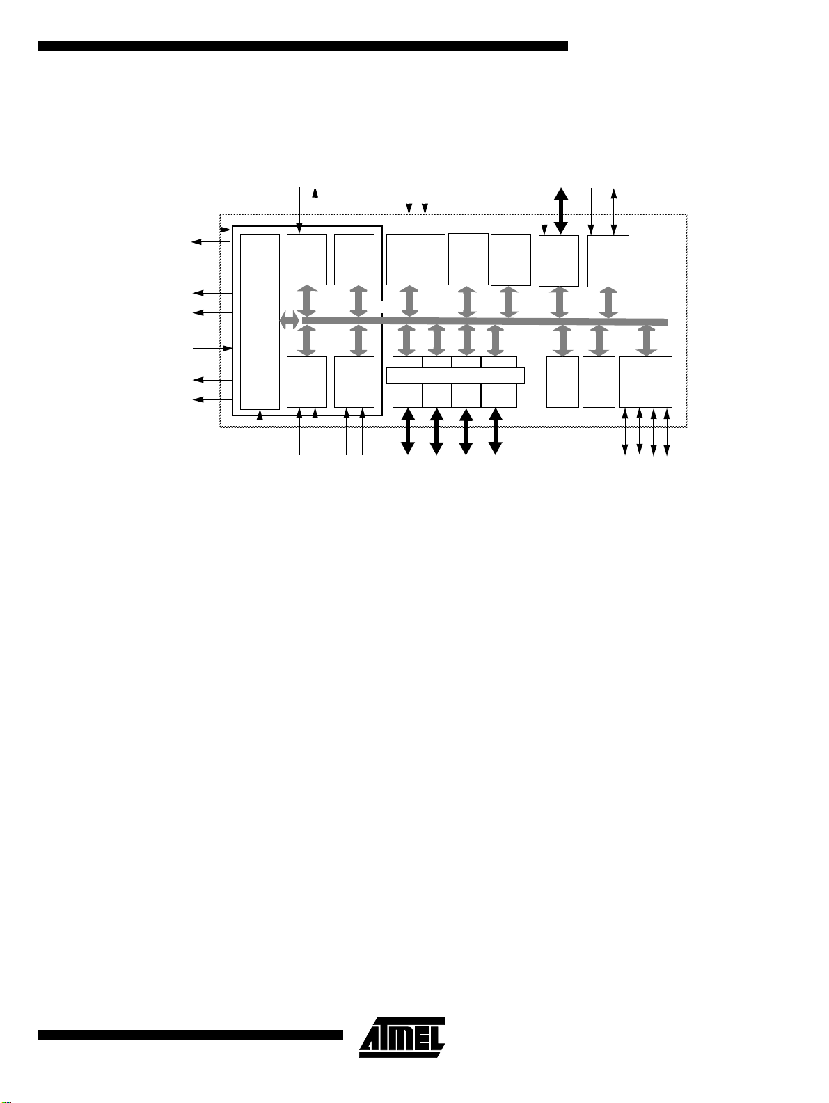
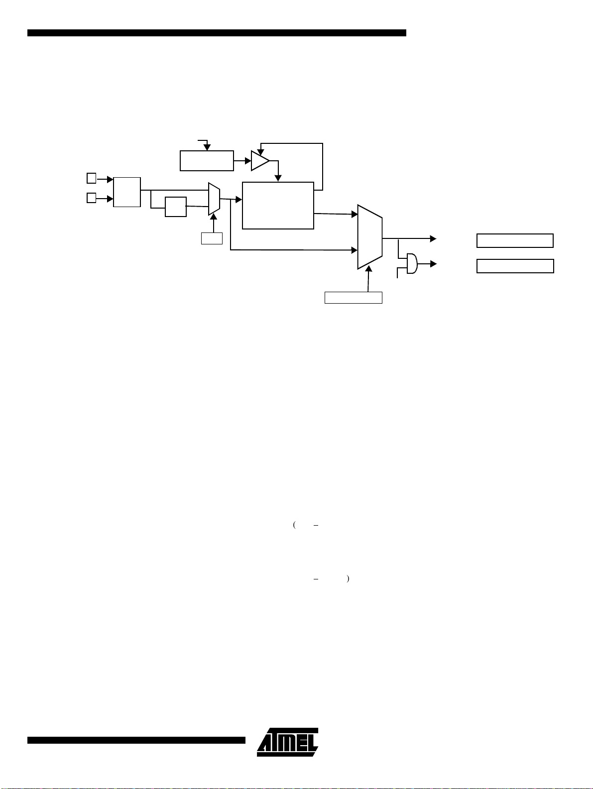
Block Diagram
Figure 1. Block Diagram
AT89C51RB2/RC2
CC
Vss
RxD
TxD
V
PCA
ECI
T2EX
T2
XTAL1
XTAL2
ALE/
PROG
PSEN
EA
(2)
RD
(2)
WR
Notes: 1. Alternate functi on of Por t 1.
2. Alternate function of Port 3.
CPU
RESET
(2)(2)
EUART
BRG
Timer 0
Timer 1
(2) (2) (2) (2)
T0
RAM
+
256x8
C51
CORE
INT
Ctrl
T1
INT0
Flash
32Kx8 or
16Kx8
IB-bus
Parallel I/O Ports & Ext. Bus
Port 0
INT1
Port 1
P0
XRAM
Port 2 Port 3
P1
1Kx8
P2
Boot
ROM
2Kx8
P3
(1)(1)
PCA
Watch
Dog
(1) (1)
Timer2
Key
Board
SPI
(1)(1) (1)
MISO
(1)
SS
MOSI
SCK
4180E–8051–10/06
3
Page 4

AT89C51RB2/RC2
SFR Mapping The Specia l Function Registers (SFRs) o f the AT89C 51RB2 /RC2 fall into t he follo wing
categories:
• C51 core registers: ACC, B, DPH, DPL, PSW, SP
• I/O port registers: P0, P1, P2, P3
• Timer registers: T2CON, T2MOD, TCON, TH0, TH1, TH2, TMOD, TL0, TL1, TL2,
RCAP2L, RCAP2H
• Serial I/O port registers: SADDR, SADEN, SBUF, SCON
• PCA (Programmable Counter Array) registers: CCON, CCAPMx, CL, CH, CCAPxH,
CCAPxL (x: 0 to 4)
• Power and clock control registers: PCON
• Hardware Watchdog Timer registers: WDTRST, WDTPRG
• Interrupt system registers: IEN0, IPL0, IPH0, IEN1, IPL1, IPH1
• Keyb oard Interface registers: KBE, KBF, KBLS
• SPI registers: SPCON, SPST R , SPDAT
• BRG (Baud Rate Generator) registers: BRL, BDRCON
• Flash register: FCON
• Clock Prescaler register: CKRL
• Others: AUXR, AUXR1, CKCON0, CKCON1
4
4180E–8051–10/06
Page 5

AT89C51RB2/RC2
Table 2. C51 Core SFRs
MnemonicAddName 76543210
ACC E0h Accumulator
B F0h B Register
PSW D0h Program Status Word CY AC F0 RS1 RS0 OV F1 P
SP 81h Stack Pointer
DPL 82h Data Pointer Low Byte
DPH 83h Data Pointer High Byte
Table 3. System Management SFRs
MnemonicAddName 76543210
PCON 87h Power Control SMOD1 SMOD0 - POF GF1 GF0 PD IDL
AUXR 8Eh Auxiliary Register 0 DPU - M0 XRS2 XRS1 XRS0 EXTRAM AO
AUXR1 A2h Auxiliary Register 1 - - ENBOOT - GF3 0 - DPS
CKRL 97h Clock Reload Register CKRL7 CKRL6 CKRL5 CKRL4 CKRL3 CKRL2 CKRL1 CKRL0
CKCKON0 8Fh Clock Control Register 0 - WDTX2 PCAX2 SIX2 T2X2 T1X2 T0X2 X2
CKCKON1AFhClock Control Register 1-------SPIX2
Table 4. Interrupt SFRs
MnemonicAddName 76543210
IEN0 A8h Interrupt Enable Control 0 EA EC ET2 ES ET1 EX1 ET0 EX0
IEN1B1hInterrupt Enable Control 1 -----ESPI EI2C KBD
IPH0 B7h Interrupt Priority Control High 0 - PPCH PT2H PHS PT1H PX1H PT0H PX0H
IPL0 B8h Interrupt Priority Control Low 0 - PPCL PT2L PLS PT1L PX1L PT0L PX0L
IPH1B3hInterrupt Priority Control High 1-----SPIHIE2CHKBDH
IPL1B2hInterrupt Priority Control Low 1-----SPILIE2CLKBDL
Table 5. Port SFRs
MnemonicAddName 76543210
P0 80h 8-bit Port 0
P1 90h 8-bit Port 1
P2 A0h 8-bit Port 2
P3 B0h 8-bit Port 3
4180E–8051–10/06
5
Page 6

AT89C51RB2/RC2
Table 6. Timer S FR s
MnemonicAddName 76543210
TCON 88h Timer/C o un te r 0 and 1 Co nt rol TF1 TR1 TF0 TR0 IE1 IT1 IE0 IT0
TMOD 89h Timer/Coun te r 0 and 1 Mo de s GATE1 C/ T1 # M11 M0 1 GATE0 C/T0# M10 M00
TL0 8Ah Timer/Counter 0 Low Byte
TH0 8Ch Timer/Counter 0 High Byte
TL1 8Bh Timer/Counter 1 Low Byte
TH1 8Dh
WDTRST A6h Watchdog Timer Reset
WDTPRGA7hWatchdog Timer Program -----WTO2WTO1WTO0
T2CON C8h Timer/Counter 2 control TF2 EXF2 RCLK TCLK EXEN2 TR2 C/T2# CP/RL2#
T2MODC9hTimer/Counter 2 Mode ------T2OEDCEN
RCAP2H CBh
RCAP2L CAh
TH2 CDh Timer/Counter 2 High Byte
TL2 CCh Timer/Counter 2 Low Byte
Timer/Counter 1 High Byte
Tim er/Cou nter 2 Reload /Cap tur e
High Byte
Tim er/Cou nter 2 Reload /Cap tur e
Low Byte
Table 7. PCA SFRs
Mnemonic
CCON D8h PCA Timer/Counter Control CF CR - CCF4 CCF3 CCF2 CCF1 CCF0
CMOD D9h PCA Timer/Counter Mode CIDL WDTE - - - CPS1 CPS0 ECF
CL E9h PCA Timer/Counter Low Byte
AddName 76543210
CH F9h PCA Timer/Counter High Byte
CCAPM0
CCAPM1
CCAPM2
CCAPM3
CCAPM4
CCAP0H
CCAP1H
CCAP2H
CCAP3H
CCAP4H
CCAP0L
CCAP1L
CCAP2L
CCAP3L
CCAP4L
DAh
PCA Timer/Counter Mode 0
DBh
PCA Timer/Counter Mode 1
DCh
PCA Timer/Counter Mode 2
DDh
PCA Timer/Counter Mode 3
DEh
PCA Timer/Counter Mode 4
FAh
PCA Compare Capture Module 0 H
FBh
PCA Compare Capture Module 1 H
FCh
PCA Compare Capture Module 2 H
FDh
PCA Compare Capture Module 3 H
FEh
PCA Compare Capture Module 4 H
EAh
PCA Compare Capture Module 0 L
EBh
PCA Compare Capture Module 1 L
ECh
PCA Compare Capture Module 2 L
EDh
PCA Compare Capture Module 3 L
EEh
PCA Compare Capture Module 4 L
6
-
CCAP0H7
CCAP1H7
CCAP2H7
CCAP3H7
CCAP4H7
CCAP0L7
CCAP1L7
CCAP2L7
CCAP3L7
CCAP4L7
ECOM0
ECOM1
ECOM2
ECOM3
ECOM4
CCAP0H6
CCAP1H6
CCAP2H6
CCAP3H6
CCAP4H6
CCAP0L6
CCAP1L6
CCAP2L6
CCAP3L6
CCAP4L6
CAPP0
CAPP1
CAPP2
CAPP3
CAPP4
CCAP0H5
CCAP1H5
CCAP2H5
CCAP3H5
CCAP4H5
CCAP0L5
CCAP1L5
CCAP2L5
CCAP3L5
CCAP4L5
CAPN0
CAPN1
CAPN2
CAPN3
CAPN4
CCAP0H4
CCAP1H4
CCAP2H4
CCAP3H4
CCAP4H4
CCAP0L4
CCAP1L4
CCAP2L4
CCAP3L4
CCAP4L4
MAT0
MAT1
MAT2
MAT3
MAT4
CCAP0H3
CCAP1H3
CCAP2H3
CCAP3H3
CCAP4H3
CCAP0L3
CCAP1L3
CCAP2L3
CCAP3L3
CCAP4L3
TOG0
TOG1
TOG2
TOG3
TOG4
CCAP0H2
CCAP1H2
CCAP2H2
CCAP3H2
CCAP4H2
CCAP0L2
CCAP1L2
CCAP2L2
CCAP3L2
CCAP4L2
PWM0
PWM1
PWM2
PWM3
PWM4
CCAP0H1
CCAP1H1
CCAP2H1
CCAP3H1
CCAP4H1
CCAP0L1
CCAP1L1
CCAP2L1
CCAP3L1
CCAP4L1
4180E–8051–10/06
ECCF0
ECCF1
ECCF2
ECCF3
ECCF4
CCAP0H0
CCAP1H0
CCAP2H0
CCAP3H0
CCAP4H0
CCAP0L0
CCAP1L0
CCAP2L0
CCAP3L0
CCAP4L0
Page 7

AT89C51RB2/RC2
Table 8. Serial I/O Port SFRs
MnemonicAddName 76543210
SCON 98h Serial Control FE/SM0 SM1 SM2 REN TB8 RB8 TI RI
SBUF 99h Serial Data Buffer
SADEN B9h Slave Address Mask
SADDR A9h Slave Address
BDRCON 9Bh Baud Rate Control BRR TBCK RBCK SPD SRC
BRL 9Ah Baud Rate Reload
Table 9. SPI Controller SFRs
MnemonicAddName 76543210
SPCON C3h SPI Control SPR2 SPEN SSDIS MSTR CPOL CPHA SPR1 SPR0
SPSTA C4h SPI Status SPIF WCOL SSERR MODF ---SPDAT C5h SPI Data SPD7 SPD6 SPD5 SPD4 SPD3 SPD2 SPD1 SPD0
Table 10. Keyboard Interface SFRs
MnemonicAddName 76543210
KBLS 9Ch Keyboard Level Selector KBLS7 KBLS6 KBLS5 KBLS4 KBLS3 KBLS2 KBLS1 KBLS0
KBE 9Dh Keyboard Input Enable KBE7 KBE6 KBE5 KBE4 KBE3 KBE2 KBE1 KBE0
KBF 9Eh Keyboard Flag Register KBF7 KBF6 KBF5 KBF4 KBF3 KBF2 KBF1 KBF0
4180E–8051–10/06
7
Page 8

AT89C51RB2/RC2
Table 11 shows all SFRs with their address and their reset value.
Ta ble 11 . S FR Mapping
Bit
addressable Non Bit addressable
0/8 1/9 2/A 3/B 4/C 5/D 6/E 7/F
F8h
CH
0000 0000
CCAP0H
XXXX
CCAP1H
XXXX
CCAPL2H
XXXX
CCAPL3H
XXXX
CCAPL4H
XXXX
FFh
F0h
E8h
E0h
D8h
D0h
C8h
C0h
B8h
B0h
A8h
A0h
98h
90h
88h
80h
1. FCON access is reserved for the Flash API and ISP software.
B
0000 0000
CL
0000 0000
ACC
0000 0000
CCON
00X0 0000
PSW
0000 0000
T2CON
0000 0000
IPL0
X000 000
P3
1111 1111
IEN0
0000 0000
P2
1111 1111
SCON
0000 0000
P1
1111 1111
TCON
0000 0000
P0
1111 1111
0/8 1/9 2/A 3/B 4/C 5/D 6/E 7/F
CMOD
00XX X000
(1)
FCON
XXXX 0000
T2MOD
XXXX XX00
SADEN
0000 0000
IEN1
XXXXX 000
SADDR
0000 0000
SBUF
XXXX XXXX
TMOD
0000 0000
SP
0000 0111
CCAP0L
XXXX XXXX
CCAPM0
X000 0000
RCAP2L
0000 0000
IPL1
XXXXX000
AUXR1
XXXXX0X0
BRL
0000 0000
TL0
0000 0000
DPL
0000 0000
CCAP1L
XXXX XXXX
CCAPM1
X000 0000
RCAP2H
0000 0000
SPCON
0001 0100
IPH1
XXXX X000
BDRCON
XXX0 0000
TL1
0000 0000
DPH
0000 0000
CCAPL2L
XXXX XXXX
CCAPM2
X000 0000
TL2
0000 0000
SPSTA
0000 0000
KBLS
0000 0000
TH0
0000 0000
CCAPL3L
XXXX XXXX
CCAPM3
X000 0000
TH2
0000 0000
SPDAT
XXXX XXXX
KBE
0000 0000
TH1
0000 0000
CCAPL4L
XXXX XXXX
CCAPM4
X000 0000
WDTRST
XXXX XXXX
KBF
0000 0000
AUXR
XX0X 0000
IPH0
X000 0000
CKCON1
XXXX XXX0
WDTPRG
XXXX X000
CKRL
1111 1111
CKCON0
0000 0000
PCON
00X1 0000
F7h
EFh
E7h
DFh
D7h
CFh
C7h
BFh
B7h
AFh
A7h
9Fh
97h
8Fh
87h
Reserved
8
4180E–8051–10/06
Page 9
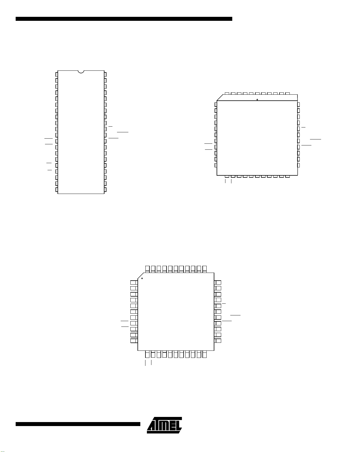
Pin Conf igurations
Figure 2. Pin Configurations
AT89C51RB2/RC2
P1.0/T2
P1.1/T2EX/SS
P1.2/ECI
P1.3CEX0
P1.4/CEX1
P1.5/CEX2/MISO
P1.6/CEX3/SCK
P1.7CEX4/MOSI
RST
P3.0/RxD
P3.1/TxD
P3.2/INT0
P3.3/INT1
P3.4/T0
P3.5/T1
P3.6/WR
P3.7/RD
XTAL2
XTAL1
VSS
1
2
3
4
5
6
7
8
9
10
11
12
13
14
15
16
17
18
19
20
PDIL40
40
39
38
37
36
35
34
33
32
31
30
29
28
27
26
25
24
23
22
21
VCC
P0.0/AD0
P0.1/AD1
P0.2/AD2
P0.3/AD3
P0.4/AD4
P0.5/AD5
P0.6/AD6
P0.7/AD7
EA
ALE/PROG
PSEN
P2.7/A15
.6/A14
P2
P2
.5/A13
12
P2.4/A
11
P2.3/A
P2.2/A
10
9
P2.1/A
P2.0/A8
P1.5/CEX2/MISO
P1.6/CEX3/SCK
P1.7/CEx4/MOSI
RST
P3.0/RxD
NIC*
P3.1/TxD
P3.2/INT0
P3.3/INT1
P3.4/T0
P3.5/T1
P1.4/CEX1
P1.3/CEX0
5 4 3 2 1 6 44 43 42 41 40
7
8
9
10
11
12
13
14
15
16
17
P1.1/T2EX/SS
P1.2/ECI
P1.0/T2
NIC*
VCC
PLCC44
P0.0/AD0
18 19 23222120 262524 27 28
NIC*
VSS
XTAL2
XTAL1
P3.7/RD
P3.6/WR
P2.0/A8
P2.1/A9
P0.1/AD1
P2.2/A10
P0.2/AD2
P2.3/A11
P0.3/AD3
39
38
37
36
35
34
33
32
31
30
29
P2.4/A12
P0.4/AD4
P0.5/AD5
P0.6/AD6
P0.7/AD7
EA
NIC*
ALE/PROG
PSEN
P2.7/A15
P2.6/A14
P2.5/A13
*NIC: No Internal Connection
4180E–8051–10/06
P1.5/CEX2/MISO
P1.6/CEX3/SCK
P1.7/CEX4/MOSI
RST
P3.0/RxD
NIC*
P3.1/TxD
P3.2/INT0
P3.3/INT1
P3.4/T0
P3.5/T1
1
2
3
4
5
6
7
8
9
10
11
P1.4/CEX1
P1.3/CEX0
43 42 41 40 3944
P1.0/T2
P1.1/T2EX/SS
P1.2/ECI
NIC*
VCC
38 37 36 35 34
VQFP44 1.4
P0.0/AD0
1213 17161514 201918 2122
VSS
NIC*
XTAL1
P3.6/WR
P3.7/RD
XTAL2
P2.0/A8
P0.2/AD2
P0.3/AD3
P0.1/AD1
P0.4/AD4
33
32
P0.5/AD5
31
P0.6/AD6
30
P0.7/AD7
29
EA
28
NIC*
27
ALE/PROG
26
PSEN
25
P2.7/A15
24
P2.6/A14
23
P2.5/A13
P2.1/A9
P2.3/A11
P2.2/A10
P2.4/A12
9
Page 10

AT89C51RB2/RC2
Table 12. Pin Description for 40 - 44 Pin Packages
Pin Number
Mnemonic
V
SS
V
CC
P0.0 - P0.7 39 - 32 43 - 36 37 - 30 I/O Port 0: Por t 0 is an open-drain, bi-directional I/O port. Port 0 pi ns that have 1s
P1.0 - P1.7 1 - 8 2 - 9 40 - 44
20 22 16 I Ground: 0V reference
40 44 38 I
1 - 3
1 2 40 I/O P1.0: Input/Output
2 3 41 I/O P1.1: Input/Output
Type Name and FunctionDIL LCC VQFP44 1.4
Power Supply: This is the power supply voltage for normal, idle and power-down
operation
written to them float and can be used as high impedance inputs. Port 0 must be
polarize d t o V
is also the multiplexed low-order address and data bus during access to external
program and data memory. In this application, it uses strong internal pull-up when
emitting 1s. Port 0 also inputs the code Bytes during Flash programming. External
pull-ups are required during program verification during which P0 outputs th e code
Bytes.
I/O Po rt 1 : Port 1 is an 8-bit bi-directional I/O port with internal pull-ups. Port 1 pins that
have 1s written to them are pulled high by the internal pull-ups and can be used as
inputs. As inputs, Port 1 pins that are externally pulled low will source current
because of the internal pull-ups. Port 1 also receives the low-order address Byte
during memory programming and verification.
Alternate functi on s for AT89C51RB2 /RC2 Port 1 include:
I/O T2 (P1.0): Timer/Counter 2 external count input/Clockout
I T2EX: Timer/Counter 2 Reload/Capture/Direction Control
or VSS in order to prevent any parasitic current consumption. Port 0
CC
I SS
3 4 42 I/O P1.2: Input/Output
I ECI: External Clock for th e PCA
4 5 43 I/O P1.3: Input/Output
I/O CEX0: Capture/Compare External I/O for PCA Module 0
5 6 44 I/O P1.4: Input/Output
I/O CEX1: Capture/Compare External I/O for PCA Module 1
6 7 1 I/O P1.5: Input/Output
I/O CEX2: Capture/Compare External I/O for PCA Module 2
I/O MISO: SPI Master Input Slave Output line
7 8 2 I/O P1.6: Input/Output
I/O CEX3: Capture/Compare External I/O for PCA Module 3
I/O SCK: SPI Serial Clock
8 9 3 I/O P1.7: Input/Output:
: SPI Slave Select
When SPI is in master mode, MISO re ceives data from the slave per ipheral. When
SPI is in slave mode, MISO outputs data to the master controller.
SCK outputs clock to the slav e peripheral
10
4180E–8051–10/06
Page 11
Table 12. Pin Description for 40 - 44 Pin Packages (Continued)
Pin Number
AT89C51RB2/RC2
Mnemonic
P1.0 - P1.7 I/O MOSI: SPI Master Output Slave Input line
XTAL1 19 21 15 I
XTAL2 18 20 14 O Cry stal 2: Output from the inverting oscillator amplifier
P2.0 - P2.7 21 - 28 24 - 31 18 - 25 I/O Port 2 : Port 2 is an 8-bit bi-directional I/O port with internal pull-ups. Port 2 pins that
P3.0 - P3.7 10 - 17 11,
13 - 19
5,
7 - 13
Type Name and FunctionDIL LCC VQFP44 1.4
I/O CEX4: Capture/Compare External I/O for PCA Module 4
When SPI is in master mode, MOSI o utputs data to the slave peripheral. When SPI
is in sla v e mode, MOSI receives data from the master contro ller .
Crystal 1: Input to the inverting oscillator amplifier and input to the internal clock
generator circuits.
have 1s written to them are pulled high by the internal pull-ups and can be used as
inputs. As inputs, Port 2 pins that are externally pulled low will source current
because of the internal pull-ups. Port 2 emits the high - order address Byte during
fetches from external program memory and during accesses to external data
memory that use 16-bit addresses (MOVX @DPTR). In this applicat ion, it uses
strong internal pull-ups emitting 1s. During accesses to external data memory that
use 8-bit addresses (MOVX @Ri ), port 2 emits the contents of the P2 SF R. Some
Port 2 pi ns receive the high order address bits during EPROM programming and
verification:
P2.0 to P2.5 for 16 KB devices
P2.0 to P2.6 for 32KB devices
I/O Po rt 3: Port 3 is an 8-bit bi-directional I/O port with internal pull-ups. Port 3 pins that
have 1s written to them are pulled high by the internal pull-ups and can be used as
inputs. As inputs, Port 3 pins that are externally pulled low will source current
because of the internal pull-ups. Port 3 also serves the special features of the
80C51 family, as listed below.
10 11 5 I RXD (P3.0): Serial in pu t por t
11 13 7 O TXD (P3.1): Serial output port
12 14 8 I INT0
13 15 9 I INT1
14 16 10 I T 0 (P3.4): Timer 0 external input
15 17 11 I T 1 (P3.5): Timer 1 external input
16 18 12 O WR
17 19 13 O RD
RST 9 10 4 I/O
ALE/PROG
30 33 27 O (I) Address Latch Enable/Program Pulse: Output pulse for latchin g the low Byt e of
(P3.2): Ex te rna l interrupt 0
(P3.3): Ex te rna l interrupt 1
(P3.6): External data memory write strobe
(P3.7): External data memory read strobe
Reset: A high on t his pin for two machine cycles while the oscillator is running,
resets the device. An internal diffused resistor to V
only an external capacitor to V
watchdog forces a system reset.
the address during an access to external memory. In normal operation, ALE is
emitted at a constant rate of 1/6 (1/3 in X2 mode) the oscillator frequency, and can
be used for external timing or clocki ng. Note that one ALE pulse is skipped during
each access to external data memory. This pin is also the program pulse input
(PROG
) duri ng Flas h p rogr a mming . ALE can be di sa bl ed by s ett in g SF R’ s AU XR. 0
bit. With this bit set, ALE will be inactive during internal fetches.
. This pin is an output when the hardware
CC
permits a power-on reset using
SS
4180E–8051–10/06
11
Page 12

AT89C51RB2/RC2
Table 12. Pin Description for 40 - 44 Pin Packages (Continued)
Pin Number
Mnemonic
PSEN 29 32 26 O Program Strobe Enable: The read strobe to external program memory. When
EA 31 35 29 I External Access Enable: EA
Type Name and FunctionDIL LCC VQFP44 1.4
executing code from the external program memory, PSEN
machine cycle, except that two PSEN
external data memory. PSEN
memory.
fetch code from external program memory locations 0000H to FFFFH (RD). If
security level 1 is programmed, EA
activ atio ns are sk ip pe d d uri ng ea ch ac ces s t o
is not activated during fetches from internal program
must be externally held low to enable the device to
will be internally latched on Reset.
is activa te d t wic e each
12
4180E–8051–10/06
Page 13
AT89C51RB2/RC2
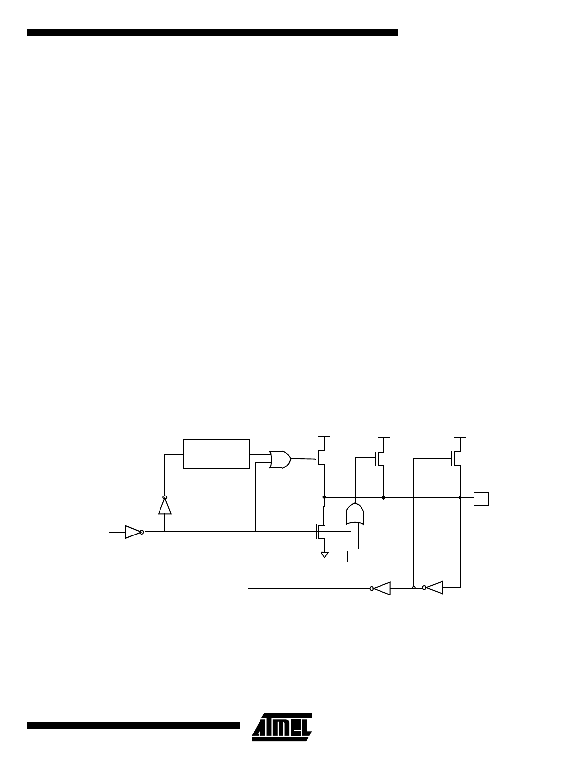
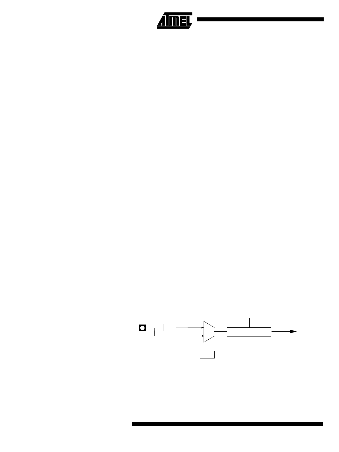
Port Types AT89C51RB2 /RC2 I/O ports (P1, P2, P3) imp lement the quasi-bid irectional o utput that
is com mon on the 8 0C 51 and mos t of its d eriva tive s. This o utp ut ty pe ca n b e used as
both an i nput and ou tput w ithout the need to rec onfigure the port. This is p ossible
because when the port outputs a logic high, it is weakly driven, allowing an external
device to pull the pin low. When the pin is pulled low, it is dri ven strongly and able to sink
a fairly large current. These features are somew hat similar to an open drain output
except that there are three pull-up transistors in the quasi-bidirectional output that serve
different purposes. One of these pul l-ups, called the "weak " pull-up, is turned on whenever the port latch for the pin contains a logic 1. The weak pull-up sources a very small
current that will pull the pin high if it is left floating. A second pull-up, called the "medium"
pull-up, is turned on when the port latch for the pin contains a logic 1 and the pin itself is
also at a logic 1 level. This pull-up provides the primary s ource current for a quas i-bidirectional pin that is outputting a 1. If a pin that has a logic 1 on it is pulled low by an
external device, the medi um pull-up turn s off, and only the we ak pull-up remains on . In
order to pull the pin low under these conditions, the external device has to sink enough
current to overpow er the me dium pull -up and take the voltage on the port pi n below its
input threshold.
The third pull-up is referred to as the "strong" pull-up. This pull-up is used to speed up
low-to-high transitions on a quasi-bidirectional port pin when the port latch changes from
a logic 0 to a logic 1. When this occurs, the strong pu ll-up turns on for a brief time, two
CPU clocks, in order to pull the port pin high quickly. Then it turns off again.
The DPU bit (bit 7 in AUXR register) allows to disable the perman ent we ak pull up of all
ports when latch data is logical 0.
The quasi-bidirectional port configuration is shown in Figure 3.
Figure 3. Quasi-Bidire ction al Output
Port Latch
Data
2 CPU
Clock Delay
Input
Data
P
N
Strong
PP
Weak
DPU
AUXR.7
Medium
Pin
4180E–8051–10/06
13
Page 14

AT89C51RB2/RC2
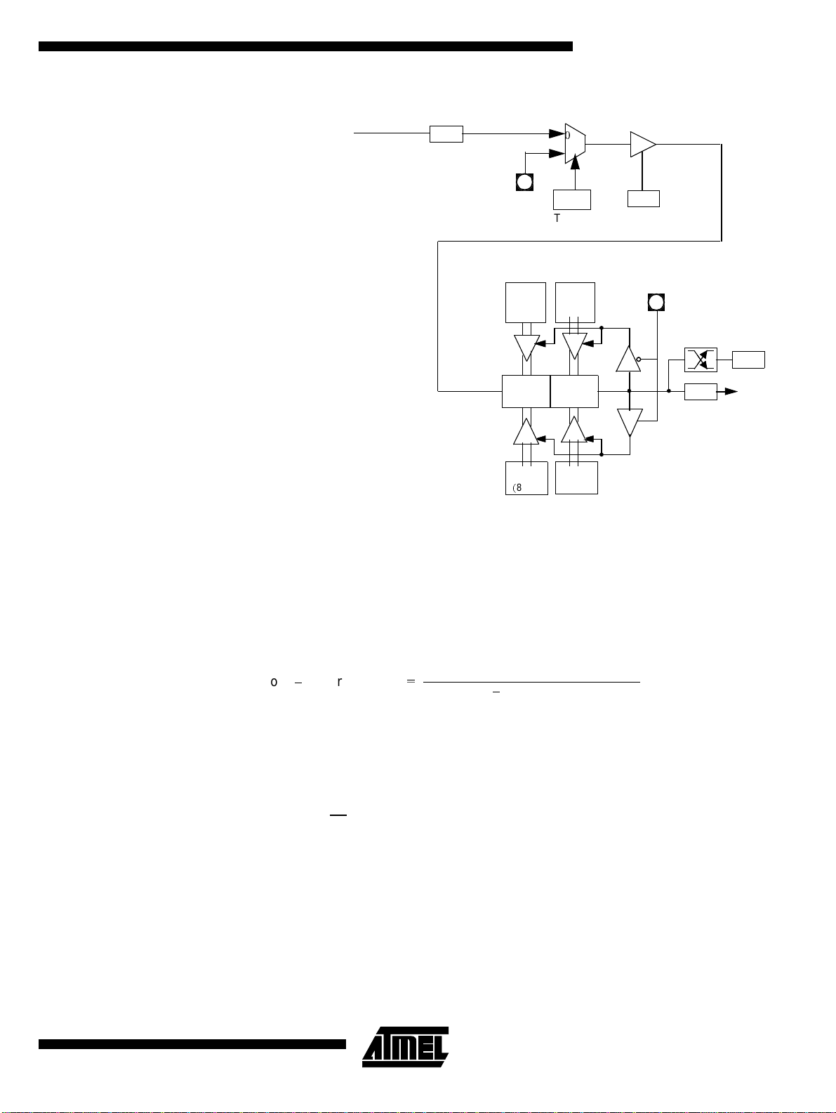
Oscillator To optim ize t he p ower c onsu mpti on an d e xecu tion ti me n eede d fo r a sp ecific task, an
internal, prescaler feature has been implemented between the oscillator and the CPU
and peripherals.
Registers Table 13. CKRL Register
CKRL – Clock Reload Register (97h)
76543210
CKRL7 CKRL6 CKRL5 CKRL4 CKRL3 CKRL2 CKRL1 CKRL0
Bit Number Mnemonic Description
7:0 CKRL
Clock Reload Register
Prescaler value
Reset Value = 1111 1111b
Not bit addressable
Table 14. PCON Register
PCON – Power Control Register (87h)
76543210
SMOD1 SMOD0 - POF GF1 GF0 PD IDL
Bit Number Bit Mnemonic Description
7SMOD1
6SMOD0
5-
4POF
Serial Port Mode bit 1
Set to select double baud rate in mode 1, 2 or 3.
Serial Port Mode bit 0
Clear ed to sel ec t SM0 bi t in SC ON r e gist er.
Set to select FE bit in SCON register.
Reserved
The value read from this bit is indeterminate. Do not set this bit.
Power-off Flag
Cleared to recognize next reset type.
Set by har dwa re wh en V
also be set by software.
rises fr om 0 to it s nomi na l volt a ge . Can
CC
14
General-pu r pos e Flag
3GF1
2GF0
1PD
0IDL
Cleared by software for general-purpose usage.
Set by software f o r ge ne r al- pu rpos e usa ge .
General-pu r pos e Flag
Cleared by software for general-purpose usage.
Set by software f o r ge ne r al- pu rpos e usa ge .
Power-down Mode bit
Cleared by hardware when reset occurs.
Set to enter power-down mode.
Idle Mode bit
Cleared by hardware when interrupt or reset occurs.
Set to enter idle mode.
Reset Value = 00X1 0000b Not bit addressable
4180E–8051–10/06
Page 15
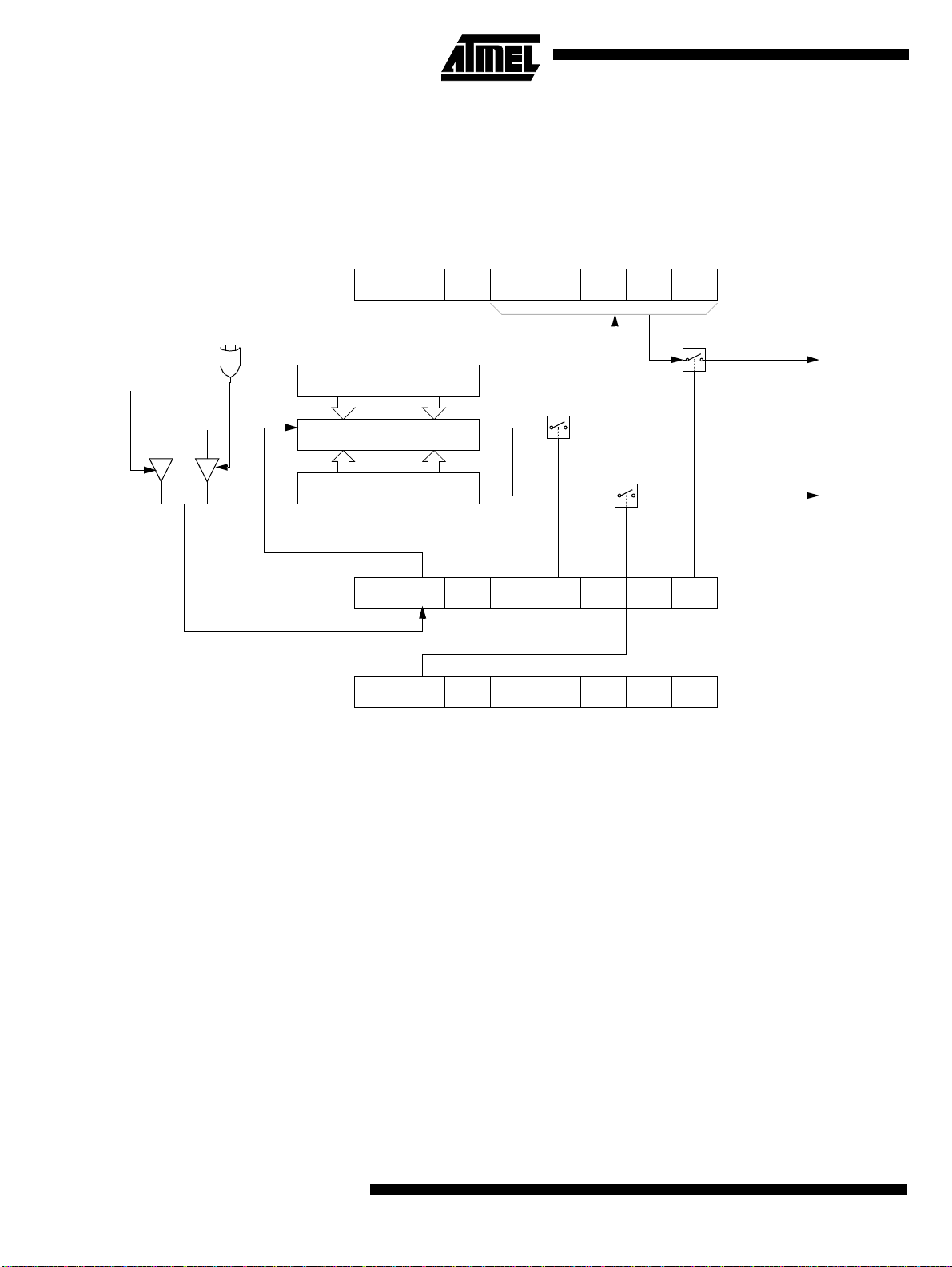
Funct ional Block
F
F
---
F
F
---
Diagram
Figure 4. Functional Oscillator Block Diagram
AT89C51RB2/RC2
Reload
8-bit
Prescaler-Divider
1
0
CKRL = 0xFF?
CLK
PERIPH
CLK
CPU
Idle
Xtal1
Xtal2
Osc
Reset
CKRL
F
OSC
1
:2
0
X2
CKCON0
Prescaler Divider • A hardware RESET puts the prescaler divider in the following state:
•CKRL = FFh: F
CLK CPU
= F
CLK PERIPH
= F
/2 (Standard C51 feature)
OSC
• Any value between F Fh down to 00h can be written by software into CKRL register
in order to divide frequency of the selected osc illator:
• CKRL = 00h: minimum frequency
F
CLK CPU
F
CLK CPU
= F
CLK PERIPH
= F
CLK PERIPH
= F
= F
/1020 (Standard Mode)
OSC
/510 (X2 Mode)
OSC
• CKRL = FFh: maximum frequenc y
F
CLK CPU
F
CLK CPU
F
CLK CPU
and F
= F
CLK PERIPH
= F
CLK PERIPH
CLK PERIPH
= F
= F
/2 (Standard Mode)
OSC
(X2 Mode)
OSC
Peripheral Clock
CPU clock
4180E–8051–10/06
In X2 Mode, for CKRL<>0xFF:
CPU
F=
CLKPERIPH
=
-------------------------------------------2 255 CKRL
OSC
–
()×
In X1 Mode, for CKRL<>0xFF then:
CPU
F=
CLKPERIPH
=
-------------------------------------------4 255 CKRL
OSC
–
()×
15
Page 16
AT89C51RB2/RC2
Enhanced Features In comparison to the original 80C52, the AT89C51RB 2/RC2 im plement s some new fea-
tures, which are
• X2 option
• Dual Data Pointer
• Extended RAM
• Programmable Counter Array (PCA)
• Hardware Watchdog
• SPI interface
• 4-level interrupt priority system
• power-off flag
• ONCE mode
• AL E disabling
• Some enha nc ed features are also located in the UART and the timer 2
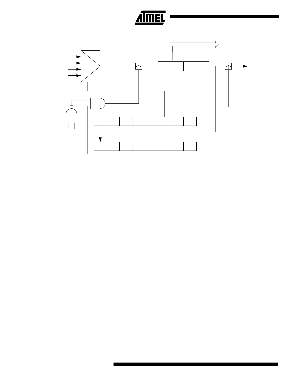
X2 Feature The AT89C51RB2/RC2 core needs only 6 clock periods per machine cycle. This feature
called ‘X2’ provides the following advantages:
• Divide frequency crystals by 2 (cheaper crystals) while keeping same CPU power.
• Save power consumption while keeping same CPU power (oscillator power saving).
• Sa ve power consum ption by dividing dynam ical ly the operating frequency by 2 in
operating and idle modes.
• Increase CPU power by 2 while keeping same crystal frequency.
:
In order to keep the original C51 compatibility, a divider by 2 is inserted between the
XTAL1 signal and the main clock input of the core (phase generator). This divider m ay
be disabled by software.
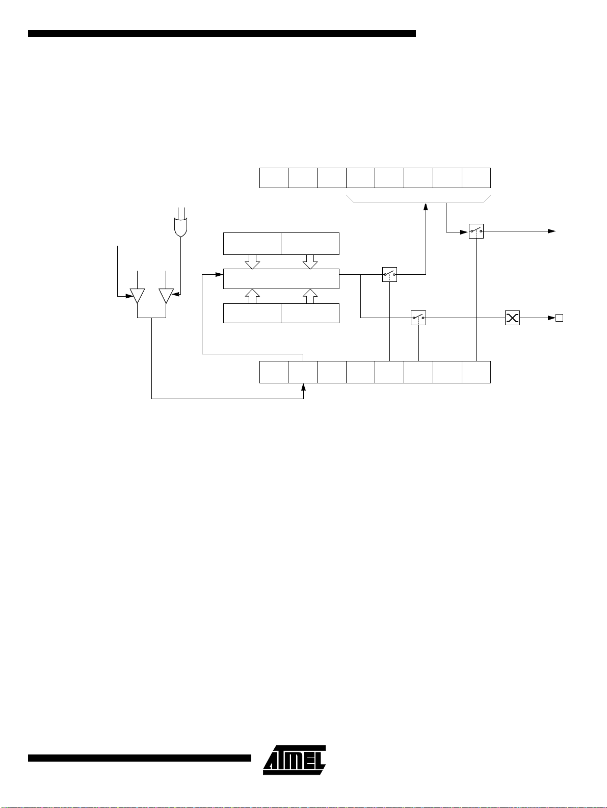
Description The clock for the w hole ci rcuit a nd peri pherals i s first divi ded by 2 before being used by
the CPU core and the peripherals.
This allows any cyclic ratio to be accepted on XTAL1 input. In X2 mode, as this divider is
bypassed, the signals on XTAL1 must have a cyclic ratio between 40 to 60%.
Figure 5 shows the clock generation block diagram. X2 bit is validated on the rising edge
of the XTAL1÷2 to avoid g litches whe n swi tching f rom X2 t o X1 mod e. Figure 6 show s
the switching mode waveforms.
Figure 5. Clock Generation Diagram
CKRL
F
X2
OSC
0
1
8 bit Pre scaler
F
CLK CPU
F
CLK PER IP H
XTAL1
FXTAL
XTAL1:2
2
CKCON0
16
4180E–8051–10/06
Page 17
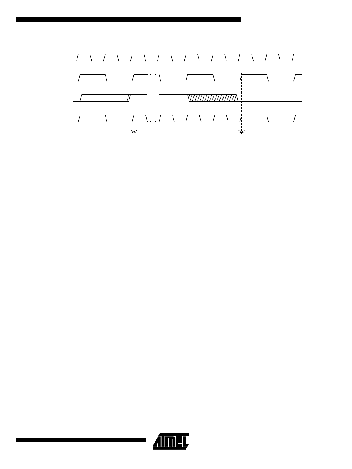
Figure 6. Mode Switching Waveforms
XTAL1
XTAL1:2
X2 Bit
CPU Clock
The X2 bit in the CKCON0 register (see Table 15) allows a switch from 12 clock periods
per instruction to 6 clo ck periods and vice versa. At reset , t he speed is set according to
X2 bit of Hardware Security Byte (HSB). By default, Standard mode is active. Setting the
X2 bit activates the X2 feature (X2 mode).
The T0X2, T1X2, T2X2, UARTX2, PCAX2, and WDX 2 bits in the CKCON0 register
(Table 15) and SPIX2 bit in the CKCON1 register (see Table 16) allow a switch from
standard peri phera l spee d ( 12 clo ck p eriod s per p eriph eral clock cyc le) to fa st pe ripheral speed (6 clock periods per peripheral clock cycle). These bits are active only in X2
mode.
AT89C51RB2/RC2
F
OSC
X2 Modex1 Mode X1 Mode
4180E–8051–10/06
17
Page 18

AT89C51RB2/RC2
Table 15. CKCON0 Register
CKCON0 - Clock Control Register (8Fh)
76543210
- WDX2 PCAX2 SIX2 T2X2 T1X2 T0X2 X2
Bit
Number
7 Reserved
6WDX2
5PCAX2
4SIX2
3T2X2
Bit
Mnemonic Description
Watchdog Clock
(This con tr ol bi t is va li da ted when t he CP U cl ock X2 i s s et ; whe n X2 is lo w, this bit
has no effect).
Cleared to select 6 clock periods per peripheral clock cycle.
Set to select 12 clock periods per peripheral clock cycle.
Programmable Counter Array Clock
(This con tr ol bi t is va li da ted when t he CP U cl ock X2 i s s et ; whe n X2 is lo w, this bit
has no effect).
Cleared to select 6 clock periods per peripheral clock cycle. Set to select 12 clock
periods per peripheral clock cycl e.
Enhanced UART Clock (Mode 0 and 2)
(This con tr ol bi t is va li da ted when t he CP U cl ock X2 i s s et ; whe n X2 is lo w, this bit
has no effect).
Cleared to select 6 clock periods per peripheral clock cycle. Set to select 12 clock
periods per peripheral clock cycl e.
Timer 2 Clock
(This con tr ol bi t is va li da ted when t he CP U cl ock X2 i s s et ; whe n X2 is lo w, this bit
has no effect).
Cleared to select 6 clock periods per peripheral clock cycle.
Set to select 12 clock periods per peripheral clock cycle.
Timer 1 Clock
2T1X2
1T0X2
0X2
(This con tr ol bi t is va li da ted when t he CP U cl ock X2 i s s et ; whe n X2 is lo w, this bit
has no effect).
Cleared to select 6 clock periods per peripheral clock cycle. Set to select 12 clock
periods per peripheral clock cycl e.
Timer0 Clock
(This con tr ol bi t is va li da ted when t he CP U cl ock X2 i s s et ; whe n X2 is lo w, this bit
has no effect).
Cleared to select 6 clock periods per peripheral clock cycle. Set to select 12 clock
periods per peripheral clock cycl e.
CPU Clock
Cleared to select 12 clock periods per machine cycle (STD, X1 mode) for CPU
and all the peripherals. Set to select 6 clock periods per machine cycle (X2
mode) and to enable the individual peripherals’X2’ bits . Programmed by
hardware after Power-up regarding Hardware Security Byte (HSB), Default
setting, X2 is cleared.
Reset Value = 0000 000’HSB. X2’b (see Table 65 “Hardware Security Byte”)
Not bit addressable
18
4180E–8051–10/06
Page 19

AT89C51RB2/RC2
Table 16. CKCON1 Register
CKCON1 - Clock Control Register (AFh)
76543210
-------SPIX2
Bit
Number
7-Reserved
6-Reserved
5-Reserved
4-Reserved
3-Reserved
2-Reserved
1-Reserved
0SPIX2
Bit
Mnemonic Description
SPI (This control bit is validated when the CPU clock X2 is set; when X2 is low,
this bit has no effect).
Clear to select 6 clock periods per peripheral clock cycle.
Set to select 12 clock periods per peripheral clock cycle.
Reset Value = XXXX XXX0b
Not bit addressable
4180E–8051–10/06
19
Page 20

AT89C51RB2/RC2
Dual Data Pointer
External Data Memory
Register (DPTR)
Figure 7. Use of Dual Pointer
AUXR1(A2H)
The addi tion al da ta poin ter ca n be u sed t o spe ed up code exe cuti on and reduc e cod e
size.
The dual D PT R st ru c tur e is a way by w h ic h the c hip will s p e c if y the address of an exter nal data memory location. There are two 16-bit DPTR registers that address the external
memory, and a single bit called DPS = AUXR1.0 (see Table 17) that allows the program
code to switch between them (see Figure 7).
07
DPS
DPTR1
DPTR0
DPH(83H) DPL(82H)
20
4180E–8051–10/06
Page 21

AT89C51RB2/RC2
Table 17. AUXR1 register
AUXR1- Auxiliary Register 1(0A2h)
76543210
- - ENBOOT - GF3 0 - DPS
Bit
Number
7-
6-
5 ENBOOT
4-
3GF3This bit is a general-purpose user flag.
20Al ways Cleared
1-
0DPS
Bit
Mnemonic Description
Reserved
The value read from this bit is indeterminate. Do not set this bit.
Reserved
The value read from this bit is indeterminate. Do not set this bit.
Enable Boot Flash
Cleare d to disa ble bo ot ROM.
Set to map the boot ROM between F800h - 0FFFFh.
Reserved
The value read from this bit is indeterminate. Do not set this bit.
(1)
Reserved
The value read from this bit is indeterminate. Do not set this bit.
Data Pointer Selection
Cleared to select DPTR0.
Set to select DPTR1.
Reset Value = XXXX XX0X0b
Not bit addressable
Note: 1. Bit 2 stuck at 0; this allows using INC AUXR1 to toggle DPS without chan ging GF3.
4180E–8051–10/06
ASSEMBLY LANGUAGE
; Block move using dual data pointers
; Modifies DPTR0, DPTR1, A and PSW
; note: DPS exits opposite of entry state
; unles s an extra INC AUXR1 is added
;
00A2 AUXR1 EQU 0A2H
;
0000 909000MOV DPTR,#SOURCE ; address of SOURCE
0003 05 A2 INC AUXR1 ; switch data pointers
0005 90 A000 MOV DPTR,#DEST ; address of DEST
0008 LOOP:
0008 05 A2 INC AUXR1 ; switch data pointers
000A E0 MOVX A,@DPTR ; get a Byte from SOURCE
000B A3 INC DPTR ; increment SOURCE address
000C 05A2 INC AUXR1 ; switch data pointers
000E F0 MOVX @DPTR,A ; write the Byte to DEST
000F A3 INC DPTR ; increment DEST address
0010 70 F6JNZ LOOP ; check for 0 t erminator
0012 05A2 INC AUXR1 ; (optional) restore DPS
21
Page 22

AT89C51RB2/RC2
INC is a short (2 Bytes) a nd fast (12 clocks) way to manipulate the DPS bit in the
AUXR1 SFR. However, note t hat the I NC i nstruction does not directly force the DPS bit
to a particular state, but simply toggles it. In simple routines, such as the block move
example, only the fact that DPS is toggled in the proper sequence matters, not its actual
value. In other words, the block move routine works the same whether DPS is '0' or '1'
on entry. Observe that without the last instruction (INC AUXR 1), the routine will ex it with
DPS in the opposite state.
22
4180E–8051–10/06
Page 23
AT89C51RB2/RC2
Expanded RAM (XRAM)
The AT89C51RB2/RC2 provides additional bytes of random access memory (RAM)
space for increased data parameter handling and high-level language usage.
AT89C51RB2/RC2 devices have expanded RAM in external data space; maximu m size
and location are described in Table 18.
Table 18. Expanded RAM
Address
Part Number XRAM Size
AT89C51RB2/RC2 1024 00h 3FFh
Start End
The AT89C51RB2/RC2 has internal data memory that is mapped into four separate
segments.
The four segments are:
1. The Lower 128 Bytes of RAM (addresses 00h to 7Fh) are directly and indirectly
addressable.
2. The Upper 128 Bytes of RAM (addresses 80h to FFh) are indirectly addressable
only.
3. The Special Function Registers, SFRs, (addresses 80h to FFh) are directly
addressable only.
4. The expanded RAM Bytes are indirectly accessed by MOVX instructions, and
with the EXTRAM bit cleared in the AUXR register (see Table 18).
The lower 128 Bytes can be accessed by either direct or indirect addressing. The Upper
128 Bytes can be accessed by indirect addressing only. The Upper 128 Bytes occupy
the same address sp ace as the S FR. Th at means they have the same addres s, but are
physically separate from SFR space.
Figure 8. Internal and External Data Memory Address
0FFh or 3FFh
XRAM
00
0FFh
128 Bytes
Indirect Accesses
80h 80h
7Fh
128 Bytes
Direct or Indirect
00
Accesses
When an instruction ac cesses an i nternal location ab ove addres s 7Fh, the CPU knows
whether the access is to the upper 128 Byte s of data RAM or to SFR space by the
addressing mode used in the instruction.
• Instructions that use direct addressing access SFR space. For example:
MOV 0A0H, # data, accesses the SFR at location 0A0h (which is P2).
Upper
Internal
RAM
Lower
Internal
RAM
0FFh
Special
Function
Register
Direct Accesses
00FFh up to 03FFh
0FFFFh
0000
External
Data
Memory
4180E–8051–10/06
23
Page 24

AT89C51RB2/RC2
• Instruc tions that use indirect addressing access the Upper 128 Bytes of data RAM.
For example: MOV @R0, # data where R0 contains 0A0h, accesses the data Byte
at address 0A0h, rather than P2 (whose address is 0A0h).
• The XRAM Bytes can be accessed by indirect addressing, with EXTRAM bit cleared
and MOVX instructions. This part of memory that is physically located on-chip,
logically occupies the first Bytes of external data memory. The bits XRS0 and XRS1
are used to hide a part of the available XRAM as explained in Table 18. This can be
useful if external peripherals are mapped at addresses already used by the internal
XRAM.
• With EXTRAM = 0,
combination with any of the registers R0, R1 of the selected bank or DPTR. An
access to XRAM will not af fect ports P0, P2, P3 .6 (WR) and P3 .7 (R D) . For
example, with EXTRAM = 0, MOVX @R0, # data where R0 contains 0A0H,
accesses the XRAM at address 0A0H rather than external memory. An access to
external data memory locations higher than the accessible size of the XRAM will be
performed with the MOVX DPTR instructions in the same way as in the standard
80C51, with P0 and P2 as data/address busses, and P3.6 and P3.7 as write and
read timing signals. Accesses to XRAM above 0FFH can only be done by the use of
DPTR.
• With EXTRAM = 1
80C51. MOVX @ Ri will provide an eight-bit address multiplexed with data on Port0
and any output port pins can be used to output higher order address bits. This is to
provide the external pag ing c apa b ili ty. MOVX @ D PTR w ill ge nerate a sixteen-bit
address. Port2 outputs the high-order eight address bits (the contents of DPH) while
Port0 multiplexes the low-order eight address bits (DPL) with data. MOVX @ RI and
MOVX @DPTR will generate either read or write signals on P3.6 (WR
(RD
).
the XRAM is indirectly addressed, using the MOVX instruction in
, MOVX @RI and MOVX @DPTR will be similar to the standard
) and P3.7
The stack pointer (SP) may be located anywhere in the 256 Bytes RAM (lower and
upper RAM) internal data memory. The stack may not be located in the XRAM.
The M0 bit allows to stretc h the XRAM tim ings; if M0 is set, the r ead and wr ite pulses
are extended from 6 to 30 clock periods. This is useful to access externa l slow
peripherals.
24
4180E–8051–10/06
Page 25

Registers Table 19. AUXR Register
AUXR - Auxiliary Register (8Eh)
76543210
DPU - M0 - XRS1 XRS0 EXTRAM AO
AT89C51RB2/RC2
Bit
Number
7DPU
6-
5M0
4-
3XRS1XRAM Size
2XRS0
1 EXTRAM
Bit
Mnemonic Description
Disable Weak Pull-up
Cleared to activate the permanent weak pull up when latch data is logical 1
Set to disactive the weak pull-up (reduce power consumption)
Reserved
The value read from this bit is indeterminate. Do not set this bit.
Pulse Length
Cleared to stretch MOVX control: the RD
periods (default).
Set to stretch MOVX control: the RD
periods.
Reserved
The value read from this bit is indeterminate. Do not set this bit.
XRS1
0 0 256 Bytes (default)
0 1 512 Bytes
1 0 768 Bytes
1 1 1024 Bytes
EXTRAM Bit
Cleared to access internal XRAM using movx @ Ri/ @ DPTR.
Set to access external memory.
Programmed by hardware after Power-up regarding Hardware Security Byte
(HSB), default setting, XRAM selecte d.
and the WR pulse length is 6 clock
and the WR pulse length is 30 clock
XRS0 XRAM size
4180E–8051–10/06
ALE Output Bit
0AO
Clear ed , ALE is em itt e d at a c onst a nt rat e of 1/6 t he osci lla to r freq ue nc y (or 1/3 if
X2 mode is used). (default) Set, ALE is active only during a MOVX or MOVC
instruc tio n is use d.
Reset Value = XX0X 00’HSB. XRAM’0b (see Table 65)
Not bit addressable
25
Page 26

AT89C51RB2/RC2
Timer 2 The Timer 2 in the AT89C51RB2/RC2 is the standard C52 Timer 2.
It is a 16-bit timer/counter: t he count is maintained by two e ight-bit timer registe rs, TH 2
and TL2 are cascaded. It is controlled by T2CON (Table 20) and T2MOD (Table 21)
registers. Timer 2 operation is similar to Timer 0 and Timer 1C/T2
operation) or external pin T2 (counter operation) as the timer clock input. Setting TR2
allows TL2 to increment by the selected input.
Timer 2 has 3 operating modes: capture, autoreload and Ba ud Rate Generator. These
modes are selected by the combination of RCLK, TCLK and CP/RL2
see the Atm el 8-bit Micro control ler Hardw are d escription f or the des criptio n of Cap ture
and Baud Rate Generator Modes.
Timer 2 includes the following enhancements:
• Auto-reload mode with up or down counter
• Programmable clock-output
selects F
(T2CON).
Auto-reload Mode The auto-re load mod e configu res T imer 2 as a 16 -bit time r or eve nt coun ter with aut o-
matic reload . If DCEN b it in T2MOD i s cleared, Timer 2 behaves as in 8 0C52 (see the
Atmel C51 Microcontroller Hardware d escription). If DCEN bit is s et, Timer 2 acts a s an
Up/down timer/counter as shown in Figure 9. In this mode the T2EX pin controls the
direction of count.
When T2EX is hi gh, Timer 2 c ounts up. T im er overf low occurs at F FF Fh which set s t he
TF2 flag and generat es an interrupt reque st. The overflow also caus es the 16-bit val ue
in RCAP2H and RCAP2L registers to be loaded into the timer registers TH2 and TL2.
/12 (timer
OSC
When T2EX is low, Timer 2 counts down. Timer underflow occurs when the count in the
timer registers TH2 and TL2 equals the value stored in RCAP2H and RCAP2L registers.
The underflow sets TF2 flag and reloads FFFFh into the timer registers.
The EXF2 bit toggles when Timer 2 overflows or underflows according to the direction of
the count. EXF2 does not generate any interrupt . This bit can be used to provide 17-bit
resolution.
26
4180E–8051–10/06
Page 27
AT89C51RB2/RC2
T
g
F
Figure 9. Auto-Reload Mode Up/Down Counter (DCEN = 1)
F
CLK PERIPH
:6
T2
0
1
C/T2
T2CON
T2CON
TR2
Programmable Clock-out Mode
(DOWN COUNTING RELOAD VALUE)
FFh
(8-bit)
TL2
(8-bit)
RCAP2L
(
8-bit)
(UP COUNTING RELOAD VALUE)
FFh
(8-bit)
TH2
(8-bit)
RCAP2H
(8-bit)
T2EX:
if DCEN = 1, 1 = UP
if DCEN = 1, 0 = DOWN
if DCEN = 0, up countin
TOGGLE
TF2
T2CON
T2CON
EXF2
TIMER 2
INTERRUP
In the clock-out mode, Timer 2 operates as a 50% duty-cycle, programmable clock generator (see Fi gure 10). The input clock incr emen ts TL2 at freq uenc y F
CLK PERIPH
/2. The
timer repeatedly counts to overflow from a loaded value. At overflow, the contents of
RCAP2H and RCAP2L registers are loaded into TH2 and TL2. In this mode, Timer 2
overflows do not generate interrupts. The formula gives the clock-out frequency as a
function of the system oscillator frequency and the value in the RCAP2H and RCAP2L
registers:
Clock O–utFrequency
-------------------------------------------------------------------------------------------- -
=
4 65536 RCAP2HRCAP2L⁄)
(×
CLKPERIPH
–
4180E–8051–10/06
For a 16 MHz system clock, Timer 2 has a programmable frequency range of 61 Hz
(F
CLK PERIPH
16
/2
) to 4 M H z (F
CLK PERIPH
/4). The generated clock signal is brought out to
T2 pin (P1.0).
Timer 2 is programmed for the clock-out mode as follows:
• Set T2OE bit in T2MOD register.
• Clear C/T 2
bit in T2CON register.
• Determine the 16-bit reload value from the formula and enter it in RCAP2H/RCAP2L
registers.
• Enter a 16-bit initial value in timer registers TH2/TL2. It can be the same as the
reload value or a different one depending on the application.
• T o start the timer, set TR2 run control bit in T2CON register.
It is possible to use Timer 2 as a baud rate generator and a clock generator simulta-
neously. For this configuration, the baud rates and clock frequencies are not
independent since both functions use the values in the RCAP2H and RCAP2L registers.
27
Page 28

AT89C51RB2/RC2
Figure 10. Clock-Out Mode C/T2 = 0
FCLK PERIPH
:6
TR2
T2CON
TL2
(8-bit)
TH2
(8-bit)
OVERFLOW
T2EX
T2
Toggle
QD
EXEN2
T2CON
RCAP2L
(8-bit)
T2MOD
EXF2
T2CON
RCAP2H
(8-bit)
T2OE
TIMER 2
INTERRUPT
28
4180E–8051–10/06
Page 29

Registers Table 20. T 2CON Register
T2CON – Timer 2 Control Register (C8h)
76543210
TF2 EXF2 RCLK TCLK EXEN2 TR2 C/T2# CP/RL2#
AT89C51RB2/RC2
Bit
Number
7 TF2
6EXF2
5 RCLK
4TCLK
3 EXEN2
2TR2
Bit
Mnemonic Description
Timer 2 Overflow Flag
Must be cleared by software.
Set by hardware on Timer 2 overflow, if RCLK = 0 and TCLK = 0.
Timer 2 External Flag
Set whe n a captur e or a reload is caused by a negative transiti on on T2EX pin if
EXEN2 = 1.
When set, causes the CPU to vector to Timer 2 interrupt routine when Timer 2
interrupt is enabled.
Must be cleared by software. EXF2 doesn’t cause an interr upt in Up/down
counter mode (DCEN = 1).
Receive Clock Bit
Cleared to use timer 1 overflow as receive clock for serial port in mode 1 or 3.
Set to use Timer 2 overflow as receive clock for serial port in mode 1 or 3.
Transmit Clock Bit
Cleare d to use time r 1 overflow as tran smit clock f or serial port in mode 1 or 3.
Set to use Timer 2 overflow as transmit clock for serial port in mode 1 or 3.
Timer 2 External Enable Bit
Cleared to ignore events on T2EX pin for Timer 2 operation.
Set to cause a capture or reload when a negative transition on T2EX pin is
detected, if Timer 2 is not used to clock the serial port.
Timer 2 Run Control Bit
Cleared to turn off Timer 2.
Set to turn on Timer 2.
4180E–8051–10/06
Timer/Coun ter 2 Select B it
1C/T2#
0CP/RL2#
Cleare d for timer operati on (input fr om inter nal clock system: F
Set for count er oper at ion (i np ut fr o m T2 inp ut pi n, fa ll i ng edg e tr igg er ). Mus t be 0
for clock out mode.
Timer 2 Capture/Reload Bit
If RCLK = 1 or TCLK = 1, CP/RL2# is ignored and timer is forced to auto-reload
on Timer 2 overflow.
Cleare d to auto-reload on Timer 2 overf lows or negative transitions on T2EX pin
if EXEN2 = 1.
Set to capture on negative transitions on T 2EX pin if EXEN2 = 1.
Reset Value = 0000 0000b
Bit addressable
CLK PERIPH
).
29
Page 30

AT89C51RB2/RC2
Table 21. T2MOD Register
T2MOD – Timer 2 Mode Control Register (C9h)
76543210
------T2OEDCEN
Bit
Number
7-
6-
5-
4-
3-
2-
1T2OE
0 DCEN
Bit
Mnemonic Description
Reserved
The value rea d fro m thi s bit is ind et erm in at e. D o no t set this bit.
Reserved
The value rea d fro m thi s bit is ind et erm in at e. D o no t set this bit.
Reserved
The value rea d fro m thi s bit is ind et erm in at e. D o no t set this bit.
Reserved
The value rea d fro m thi s bit is ind et erm in at e. D o no t set this bit.
Reserved
The value rea d fro m thi s bit is ind et erm in at e. D o no t set this bit.
Reserved
The value rea d fro m thi s bit is ind et erm in at e. D o no t set this bit.
Timer 2 Output Enable Bitt
Cleared to program P1.0/T2 as clock input or I/O port.
Set to program P1.0/T2 as clock output.
Down Counter Enable Bit
Cleare d to disable Timer 2 as up/down counter.
Set to enable Timer 2 as up/down counter.
Reset Value = XXXX XX00b
Not bit addressable
30
4180E–8051–10/06
Page 31

AT89C51RB2/RC2
Programmable Counter Array (PCA)
The PCA provides more timing capabilities with less CPU intervention than the standard
timer/counters. Its adva ntages in clude reduc ed software ove rhead and improve d accuracy. The PCA consis ts of a dedicated tim er/counter which serv es as the time bas e for
an array of five com pare/ca pture Modu les. Its clock i nput can b e program med to count
any one of the following signals:
• Peripheral clock frequen cy (F
• Peripheral clock frequen cy (F
CLK PERIPH
CLK PERIPH
) ÷ 6
) ÷ 2
• Timer 0 overflow
• External input on ECI (P1.2)
Each compare/capture Modules can be programmed in any one of the following modes:
• Rising and/or falling edge capture
• Software timer
• High-speed output
• Pulse width modulat or
Module 4 ca n also be pro grammed as a w atchd og time r (see Se ction "PCA Wa tchdo g
Timer", page 42).
When the compare/capture Modules are programmed in the capture mode, software
timer, or high speed output m ode, an interrupt can be generated when the Module executes its function. All five Module s plus the PCA timer overflow share one interrupt
vector.
The PCA timer/counter and compare/capture modules share Port 1 for external I/O.
These pins a re listed belo w. If one or sev eral bits in the po rt are not used for the PCA,
they can still be used for standard I/O.
PCA Component External I/O Pin
16-bit Counter P1.2/ECI
16-bit Module 0 P1.3/CEX0
16-bit Module 1 P1.4/CEX1
16-bit Module 2 P1.5/CEX2
16-bit Module 3 P1.6/CEX3
The PC A ti mer is a co mm on t ime b as e fo r all f ive M odu les ( see Fig ure 11). The ti mer
count source is determined from the CPS1 and CPS0 bits in the CMOD register
(Table 22) and can be programmed to run at:
• 1/6 the
• 1/2 the
periphera l c loc k f requency (F
periphera l c loc k f requency (F
CLK PERIPH
CLK PERIPH
)
)
• The Timer 0 overflow
• The input on the ECI pin (P1.2)
4180E–8051–10/06
31
Page 32
AT89C51RB2/RC2
Figure 11. PCA Timer/Counter
To PCA
Modules
F
CLK PERIPH
F
CLK PERIPH
T0 OVF
Idle
P1.2
/6
It
CMOD
0xD9
CCON
0xD8
overflow
/2
CIDL CPS1 CPS0 ECF
WDTE
CF CR
CCF4 CCF3 CCF2 CCF1 CCF0
CH CL
16-bit up Counter
32
4180E–8051–10/06
Page 33

Registers Table 22. CM OD Register
CMOD – PCA Counter Mode Register (D9h)
76543210
CIDL WDTE - - - CPS1 CPS0 ECF
AT89C51RB2/RC2
Bit
Number
7CIDL
6WDTE
5-
4-
3-
2 CPS1 PCA Count Pulse Select
1 CPS0
0ECF
Bit
Mnemonic Description
Counter Idle Co ntrol
Cleared to program the PCA Counter to continue functioning during idle Mode.
Set to program PCA to be gated off during idle.
Watchdog Timer Enable
Cleared to disable Watchdog Timer function on PCA Modul e 4.
Set to enable Watchdog Timer function on PCA Module 4.
Reserved
The value read from this bit is indeterminate. Do not set this bit.
Reserved
The value read from this bit is indeterminate. Do not set this bit.
Reserved
The value read from this bit is indeterminate. Do not set this bit.
CPS0 Selected PCA input
CPS1
0 0 Internal clock F
0 1 Internal clock F
1 0 Timer 0 Over flow
1 1 External cl ock at ECI/P1.2 pin (max rate = fCLK PERI PH / 4)
PCA Enable Counter O ve rflow Inte rrupt
Cleared to disable CF bit in CCON to inhibit an interrupt.
Set to enable CF bit in CCON to generate an interrupt.
CLK PERIPH
LK PERIPH
/6
/2
4180E–8051–10/06
Reset Value = 00XX X000b
Not bit addressable
The CMOD register includes three additional bits associated with the PCA.
• The CIDL bit which allows the PCA to stop during idle mode.
• The WDT E bit which enables or disables the watchdog function on Mo dule 4.
• The ECF bit which when set causes an interrupt and the PCA overflow flag CF (in
the CCON SFR) to be set when the PCA timer overflows.
The CCON register contains the run control bit for the PCA and the flags for the PCA
timer (CF) and each Module (see Table 23).
• Bit CR (CCON. 6) must be set by software to run the PCA. The PCA is shut off by
clearing this bit.
• Bit CF: The CF bit (CCON. 7) is set when the PCA counter overflows and an
interrupt will be generated if the ECF bit in the CMOD register is set. The CF bit can
only be cleared by software.
• Bits 0 through 4 are the flags for the Modules (bit 0 for Module 0, bit 1 for Module 1,
etc. ) and are set by hardware when either a match or a capture occurs. These flags
also can only be cleared by software.
33
Page 34

AT89C51RB2/RC2
Table 23. CCON Register
CCON – PCA Counter Control Register (D8h)
76543210
CF CR - CCF4 CCF3 CCF2 CCF1 CCF0
Bit
Number
7CF
6CR
5-
4 CCF4
3 CCF3
2 CCF2
1 CCF1
Bit
Mnemonic Description
PCA Counter Overflow Flag
Set by hardware when the counter rolls over. CF flags an interrupt if bit ECF in
CMOD is set. CF may be set by either hardware or software but can only be
cleared by software.
PCA Counter Run Control Bit
Must be cleared by software to turn the PCA counter off.
Set by software to turn the PCA counter on.
Reserved
The value read from this bit is indeterminate. Do not set this bit.
PCA Module 4 Interrupt Flag
Must be cleared by software.
Set by hardware when a match or capture occurs.
PCA Module 3 Interrupt Flag
Must be cleared by software.
Set by hardware when a match or capture occurs.
PCA Module 2 Interrupt Flag
Must be cleared by software.
Set by hardware when a match or capture occurs.
PCA Module 1 Interrupt Flag
Must be cleared by software.
Set by hardware when a match or capture occurs.
34
PCA Module 0 Interrupt Flag
0 CCF0
Must be cleared by software.
Set by hardware when a match or capture occurs.
Reset Value = 000X 0000b
Bit addressable
The watchdog timer function is implemented in Module 4 (see Figure 14).
The PCA interrupt system is shown in Figure 12.
4180E–8051–10/06
Page 35
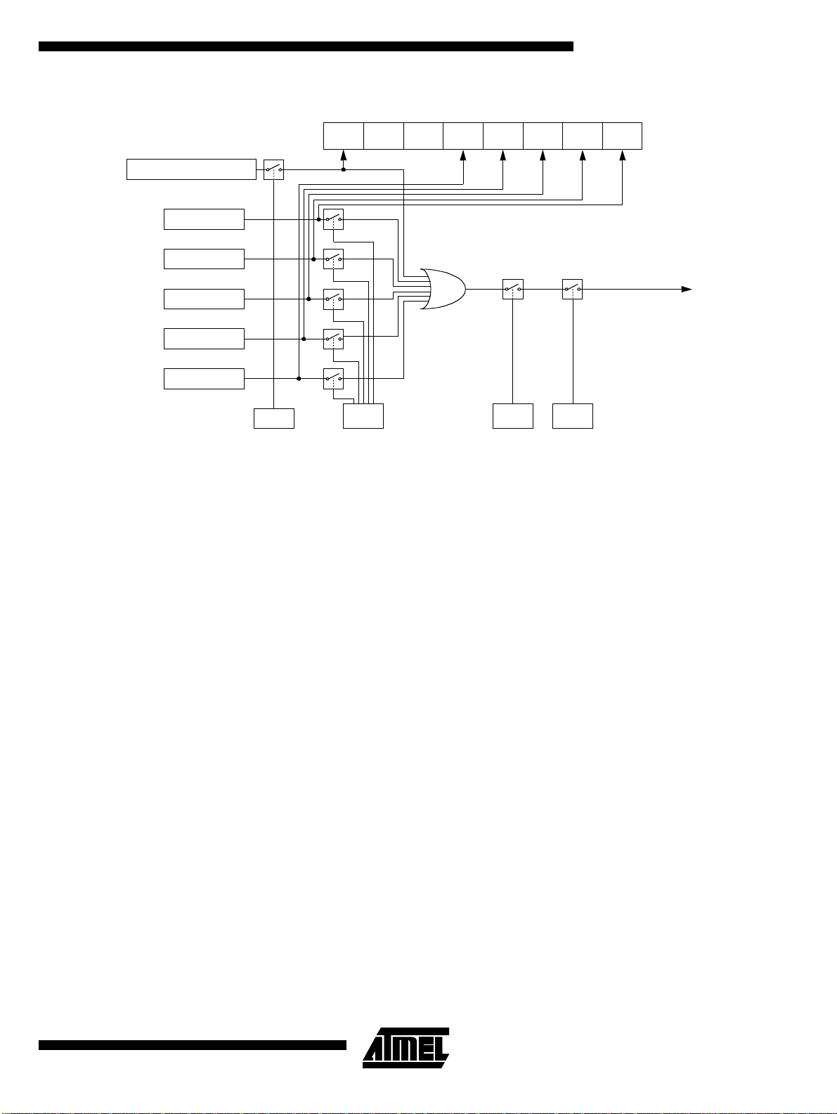
Figure 12. PC A Interru p t System
PCA Timer/Coun ter
Module 0
CF CR
AT89C51RB2/RC2
CCF4 CCF3 CCF2 CCF1 CCF0
CCON
0xD8
Module 1
Module 2
Module 3
Module 4
To Interrupt
Priority Decoder
ECF
ECCFn
CCAPMn. 0CMOD. 0
IEN0. 6 IEN0. 7
EC EA
PCA Modules: each one of th e fiv e com pare /cap ture Mo dule s ha s si x pos sibl e func tions. It can perform:
• 16-bit Capture, positive-edge triggered
• 16-bit Capture, negative-edge triggered
• 16-bit Capture, both positive and negative-ed ge triggered
• 16-bit Software Timer
• 16-bit High-speed Output
• 8-bit Pulse Width Modulator
In addition, Module 4 can be used as a Watchdog Timer.
Each Module in the PCA has a special function register associated with it. These regis-
ters are: CC APM0 f or Modu le 0, CCA PM1 for M odule 1, e tc. (see T able 24). The
registers contain the bits that control the mode that each Module will operate in.
• The ECCF bit (CCAPMn. 0 where n = 0, 1, 2, 3, or 4 depending on the Module)
enables the CCF flag in the CCON SFR to generate an interrupt when a match or
compare occurs in the associated Module.
• PW M (CCAPMn. 1) enables the pulse width modulation mode.
• The TOG bit (CCAPMn. 2) when set causes the CEX output associated with the
Module to toggle when there is a match between the PCA counter and the Module's
capture/compare register.
• The match bit MAT (CCAPMn. 3) when set will cause the CCFn bit in the CCON
register to be set when there is a match between the PCA counter and the Module's
capture/compare register.
• The next two bits CAPN (CCAPMn. 4) and CAPP (CCAPMn. 5) determine the edge
that a capture input will be active on. The CAPN bit enables the negative edge, and
the CAPP bit enables the positive edge. If both bits are set both edges will be
enabled and a capture will occur for either transit ion.
• The last bit in the register ECOM (CCAPMn. 6) when set enables the comparator
function.
4180E–8051–10/06
Table 24 shows the CCAPMn settings for the various PCA functions.
35
Page 36

AT89C51RB2/RC2
Table 24. CCAPMn Registers (n = 0-4)
CCAPM0 – PCA Module 0 Compare/Capture Control Register (0DAh)
CCAPM1 – PCA Module 1 Compare/Capture Control Register (0DBh)
CCAPM2 – PCA Module 2 Compare/Capture Control Register (0DCh)
CCAPM3 – PCA Module 3 Compare/Capture Control Register (0DDh)
CCAPM4 – PCA Module 4 Compare/Capture Control Register (0DEh)
76543210
- ECOMn CAPPn CAPNn MATn TOGn PWMn ECCFn
Bit
Number
7-
6ECOMn
5 CAPPn
4 CAPNn
3MATn
2 TOGn
1PWMn
Bit
Mnemonic Description
Reserved
The value read from this bit is indeterminate. Do not set this bit.
Enable Comparator
Cleared to disable the comparator function.
Set to enable the comparator function.
Capture Positiv e
Cleared to disable positive edge capture.
Set to enable positive edge capture.
Capture Negati ve
Cleared to disable negative edge capture.
Set to enable negative edge capture.
Match
When MATn = 1, a match of the PCA counter with this Module's
compare/capture reg ister cau s es the CCFn bit in CCON to be set, flagging an
interrupt.
Toggle
When TOGn = 1, a match of the PCA counter with this Module's
compare/capture register causes theCEXn pin to toggle.
Pul s e Width Modulation Mode
Cleared to disable the CEXn pin to be used as a pulse width modulated output.
Set to enable the CEXn pin to be used as a pulse width modulated output.
36
Enable CCF Interrupt
0 CCF0
Clear ed to disa bl e comp ar e /cap t ure f la g CCFn in t he CCON regi st er t o ge ne rat e
an interrupt.
Set to enable compare/capture flag CCFn in the CCON register to generate an
interrupt.
Reset Value = X000 0000b
Not bit addressable
4180E–8051–10/06
Page 37

AT89C51RB2/RC2
Table 25. PCA Module Modes (CCAPMn Registers)
ECOMn CAPPn CAPNn MATn TOGn PWMm ECCFn Module Function
0000000 No Operation
X10000X
X01000X
X11000X
100100X
100110X 16-bit High-speed Output
1000010 8-bit PWM
1001X0X Watchdog Timer (Module 4 only)
16-bit capture by a positive-edge
trigger on CEXn
16-bit captur e by a negative trigger
on CEXn
16-bit capture by a transition on
CEXn
16-bit Software Timer/Compare
mode.
There are two a dditiona l regist ers associ ated with eac h of the PCA Mo dules. The y are
CCAPnH and CCAPnL and these are the registers that store the 16-bit count when a
capture oc curs or a com pare shou ld oc cur. W hen a M odul e is used in the P WM mod e
these registers are u sed to control the duty cycle of the output (see Table 26 and
Table 27).
Table 26. CCAPnH Registers (n = 0-4)
CCAP0H – PCA Module 0 Compare/Capture Control Register High (0FAh)
CCAP1H – PCA Module 1 Compare/Capture Control Register High (0FBh)
CCAP2H – PCA Module 2 Compare/Capture Control Register High (0FCh)
CCAP3H – PCA Module 3 Compare/Capture Control Register High (0FDh)
CCAP4H – PCA Module 4 Compare/Capture Control Register High (0FEh)
76543210
--------
Bit
Number
7 - 0 -
Bit
Mnemonic Description
PCA Module n Compare/Capture Control
CCAPnH Value
Reset Value = 0000 0000b
Not bit addressable
4180E–8051–10/06
37
Page 38

AT89C51RB2/RC2
Table 27. CCAPnL Registers (n = 0-4)
CCAP0L – PCA Module 0 Compare/Capture Control Register Low (0EAh)
CCAP1L – PCA Module 1 Compare/Capture Control Register Low (0EBh)
CCAP2L – PCA Module 2 Compare/Capture Control Register Low (0ECh)
CCAP3L – PCA Module 3 Compare/Capture Control Register Low (0EDh)
CCAP4L – PCA Module 4 Compare/Capture Control Register Low (0EEh)
76543210
--------
Bit
Number
7 - 0 -
Bit
Mnemonic Description
PCA Module n Compare/Capture Control
CCAPnL Value
Reset Value = 0000 0000b
Not bit addressable
Table 28. CH Register
CH – PCA Counter Register High (0F9h)
76543210
--------
Bit
Number
7 - 0 -
Bit
Mnemonic Description
PCA Counter
CH Value
Reset Value = 0000 0000b
Not bit addressable
Table 29. CL Register
38
CL – PCA Counter Register Low (0E9h)
76543210
--------
Bit
Number
7 - 0 -
Bit
Mnemonic Description
PCA Counter
CL Value
Reset Value = 0000 0000b
Not bit addressable
4180E–8051–10/06
Page 39
AT89C51RB2/RC2
PCA Capture Mode To use on e of the PCA M odules in the capture m ode either one or bo th of the CCAP M
bits CAPN and CAPP f or that Module must be set. The external CEX input for t he M odule (on po rt 1) is sam pled for a transiti on. Wh en a valid t ransition occurs t he PCA
hardware l oads the value of th e PC A cou nte r regi sters ( CH and CL) i nto th e Mo dule's
capture registers (CCAPnL and CCAP nH). If the CCFn bit for the Modul e in the CCON
SFR and the ECCFn bit in the CCAPMn SFR are set then an interrupt will be generated
(see Figure 1 3).
Figure 13. PCA Capture Mode
Cex. n
CF CR
ECOMn
CCF4 CCF3 CCF2 CCF1 CCF0
Capture
CAPNn MATn TOGn PWMn ECCFnCAPPn
CCON
0xD8
PCA IT
PCA Counter/Timer
CH CL
CCAPnH CCAPnL
CCAPMn, n = 0 to 4
0xDA to 0xDE
4180E–8051–10/06
39
Page 40
AT89C51RB2/RC2
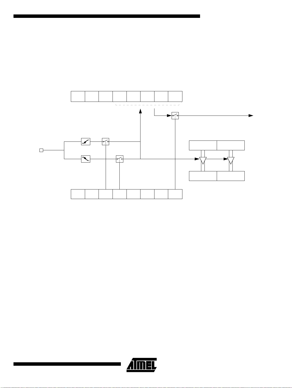
16-bit Software Timer/ Compare Mode
The PCA Modules can be used as software timers by setting both the ECOM and M AT
bits in the Modules CCAPMn register. The PCA timer will be compared to the Module's
capture registers and wh en a ma tch occurs, an i nterrup t will occur if the CCFn (CCO N
SFR) and the ECCFn (CCAPMn SFR) bits for the Module are both set (see Figure 14).
Figure 14. PCA Compare Mode and PCA Wat chdog Timer
CF CCF2 CCF1 CCF0
CR
CCF4
CCF3
CCON
0xD8
Write to
CCAPnH
Write to
CCAPnL
10
Reset
Enable
PCA IT
CCAPnH CCAPnL
Match
16 bit Comparator
(1)
CH CL
PCA Counte r/Timer
ECOMn
CIDL CPS1 CPS0 ECF
WDTE
CAPNn MATn TOGn PWMn ECCFnCAPPn
CCAPMn, n = 0 to 4
0xDA to 0xDE
CMOD
0xD9
RESET
Note: 1. Only for Module 4
Before enabling ECOM b it, CCAPnL and CCAPnH should be set with a non z ero value,
otherwise an unwanted match could occur. Writing to CCAPnH will set the ECOM bit.
40
Once ECOM set, writin g CCAPnL will clear E COM so that an un wanted ma tch doe sn’t
occur while modifying the compare value. Writing to CCAPnH will set ECOM. For this
reason, user software should write CCAPnL first, and then CCAPnH. Of course, the
ECOM bit can still be controlled by accessing to CCAPMn register.
4180E–8051–10/06
Page 41
AT89C51RB2/RC2
High-speed Output Mode In t his mode the CEX output (on port 1) as sociated with the PCA module will toggle
each time a match occurs between the PCA counter and the modules capture registers.
To activate this mode the TOG, MAT, and ECOM bits in the modules CCAPMn SFR
must be set (see Figure 15).
A prior write must be done to CCAPnL and CCAPnH before writing the ECOMn bit.
Figure 15. PCA High-speed Output Mode
CCON
0xD8
PCA IT
Write to
CCAPnH
Write to
CCAPnL
Reset
CF CR
CCAPnH CCAPnL
CCF4 CCF3 CCF2 CCF1 CCF 0
0
1
Enable
16-bit Comparator
CH CL
PCA Counte r/Timer
ECOMn
Match
CAPNn MATn TOGn PWMn ECCFnCAPPn
CEXn
CCAPMn, n = 0 to 4
0xDA to 0xDE
Before enabling ECOM bit, CCAPnL and CCAPnH should be set with a non-zero value,
otherwise an unwanted match could occur.
Once ECOM is set, writing CCAPnL will clear ECOM so that an unwanted match doesn’t
occur while modifying the compare value. Writing to CCAPnH will set ECOM. For this
reason, user software should write CCAPnL first, and then CCAPnH. Of course, the
ECOM bit can still be controlled by accessing to CCAPMn register.
4180E–8051–10/06
41
Page 42

AT89C51RB2/RC2
Pulse Width Modulator Mode
All of the PCA Modules can be used as PWM outputs. Fi gure 16 shows the PW M func tion. The frequency of the output depends on the source for the PCA timer. All of the
Modules will have the sam e freque ncy of output be cause they all share the PCA timer.
The duty cycle of each Module is independently variable using the module's capture
register CCAPLn. When the value of the PCA CL SFR is less than the value in the module's CCAPLn SFR the output will be low, when it is equal to or greater than the output
will be hig h. Wh en CL ov erfl ows f rom FF t o 00 , CC APL n is r eloa de d wi th th e val ue i n
CCAPHn. This allows updat ing the PWM without glitches . The PWM and E COM bits in
the module's CCAPMn register must be set to enable the PWM mode.
Figure 16. PCA PWM Mode
CCAPnH
CCAPnL
8-bit Com p arator
CL
PCA Counter/Timer
“0”
CEXn
“1”
CCAPMn, n = 0 to 4
0xDA to 0xDE
ECOMn
Overflow
Enable
CAPNn MATn TOGn PWMn ECCFnCAPPn
PCA Watchdog Timer An on-board watchdog timer is available with the PCA to improve the reliability of the
system without increasing chip count. Watchdog timers are useful for systems that are
susceptible to noise, power glitches, or electrostatic discharge. Module 4 is the only
PCA Module that can be programmed as a watchdog. Howev er, this Module can s till be
used for other modes if the watchd og is not needed. Figure 14 shows a d iagram of how
the watchdog works. The user pre-loads a 16-bit value in the compare registers. Just
like the other compare modes, this 16-bit value is compared to the PCA timer value. If a
match is allowed to occur, an internal reset will be generated. This will not cause the
RST pin to be driven high.
42
In order to hold off the reset, the user has the following three options:
1. Periodically change the compare value so it will never match the PCA timer.
2. Periodically change the PCA timer value so it will never match the compare
values.
3. Disable the watchdog by clearing the WDTE bit before a match occurs and then
re-enable it.
The first two options are more reliable because th e watchdo g timer is never disabl ed as
in option #3. If the program c ounter ev er g oes ast ray, a ma tch will eventu ally occur and
cause an internal reset. The second option is also not recommended if other PCA Modules are being used. Remember, the PCA timer is the time base for all modules;
4180E–8051–10/06
Page 43

AT89C51RB2/RC2
changing the time base for other Modules would not be a good idea. Thus, in most applications the first solution is the best option.
This watchdog timer won’t generate a reset out on the reset pin.
4180E–8051–10/06
43
Page 44

AT89C51RB2/RC2
Serial I/O Port The serial I/O port in the AT89C51RB2/RC2 is compatible with the serial I/O port in the
80C52.
It provides both synchronous and asynchronous communication modes. It operates as a
Universal Asynchronous Receiver and Transmitter (UART) in three full-duplex modes
(Modes 1, 2 and 3). Asynchronous transmission and reception can occur simultaneously
and at different baud rates
Serial I/O port includes the following enhancements:
• Framing error detection
• Automatic address recognition
Framing Error Detection Framing bi t error de tect ion is pro vid ed for t he three asyn chro nous m odes (m odes 1, 2
and 3). To enable the framing bit error detection feat ure, set SMOD0 bit in PCON register (See Figure 17).
Figure 17. Framing Error Block Diagram
RITIRB8TB8RENSM2SM1SM0/FE
SCON (98h)
Set FE bit if stop bit is 0 (framing error) (SMOD0 = 1)
SM0 to UART mode control (SMOD0 = 0)
PCON (87h)
IDLPDGF 0GF1POF-SMOD0SMOD1
To UART framing error control
When this feature is enabl ed, the receiver chec ks each incoming da ta frame for a valid
stop bit. An invalid stop bit may result from noise on the serial lines or f rom simultaneous
transmissio n by two C PUs . If a valid stop bit is n ot found, t he Frami ng Error bit (FE) in
SCON register (See Table 33.) bit is set.
Software may exam ine FE b it after each reception to check for data errors. O nce set,
only software or a reset can clear FE bi t. Subsequ ently received frames with valid stop
bits cannot clear FE bit. When FE feature is enabled, RI rises on stop bit instead of the
last data bit (See Figure 18. and Figure 19.).
Figure 18. UART Timings in Mode 1
RXD
RI
SMOD0=X
FE
SMOD0=1
Start
bit
Data byte
D7D6D5D4D3D2D1D0
Stop
bit
44
4180E–8051–10/06
Page 45

Figure 19. UART Timings in Modes 2 and 3
AT89C51RB2/RC2
Automatic Address Recognition
RXD
RI
SMOD0=0
RI
SMOD0=1
FE
SMOD0=1
Start
bit
Data byte Ninth
D8D7D6D5D4D3D2D1D0
Stop
bit
bit
The automatic address rec og nition feat ure is e nabled when the multiprocessor comm unication feature is enabled (SM2 bit in SCON register is set).
Implemented in hardw are, auto matic add ress recog nition enh ances the multipro cessor
communication feature by allowing the serial port to examine the address of each
incoming command frame. Only when the serial port recognizes its own address, the
receiver sets RI bit in SCON register to generate an interrupt. This ensures that the CPU
is not interrupted by command frames addressed to other devices.
If desired, the user may ena ble the a utomatic addres s recognit ion feature in m ode 1.In
this configuration, the stop bit takes the place of the ninth data bit. Bit RI is set only when
the received com mand fr ame ad dress matc hes the de vice’s addres s and is term inated
by a valid stop bit.
To support automatic addres s rec ognition, a dev i ce is identified b y a given ad dres s and
a broadcast address.
Note: The multiprocessor communication and automatic address recognition features cannot
be enabled in mode 0 (i. e. sett ing SM2 bit in SCON register in mode 0 has no effect).
Given Address Each de vice has an individual address that is specified in SADDR register; the SADEN
register i s a mask byt e that conta ins don’t-c are bits (d efined b y zeros) to for m the
device’s given address. The don’t-care bits provide the flexibility to address one or more
slaves at a time. The follow ing ex am ple illu str at es how a given address is form ed.
To address a device by its individual address, the SADEN mask byte must be 1111
1111b.
For example:
SADDR0101 0110b
SADEN
1111 110 0b
Given0101 01XXb
The following is an example of how to use given addresses to address different slaves:
Slave A:S A D D R1111 00 01b
SADEN
1111 10 10b
Given1111 0X0Xb
Slave B:SADDR1111 0011b
SADEN
1111 10 01b
Given1111 0XX1b
Slav e C :S ADDR1111 0010b
SADEN
1111 110 1b
Given1111 00X1b
4180E–8051–10/06
45
Page 46

AT89C51RB2/RC2
The SADEN byte is selected so that each slave may be addressed separately.
For slave A, bit 0 (the LSB) is a don’t-care bit; for slaves B and C, bit 0 is a 1.To communicate with slave A only, the master must send an address where bit 0 is clear (e. g.
1111 0000b).
For slave A, bit 1 is a 1; for slaves B and C, bit 1 is a don’t care bit. To communicate with
slaves B and C, but not slave A, the master must send an address with bits 0 and 1 both
set (e. g. 1111 0011b).
To communicate with slaves A, B and C, the master must send an address with bit 0 set,
bit 1 clear, and bit 2 clear (e. g. 1111 0001b).
Broadcast Address A broadcast address is formed from the logical OR of the SADDR and SADEN registers
with zeros defined as don’t-care bits, e. g. :
SADDR0101 0110b
SADE N1111 1100b
Broadcast =SADDR OR SADEN1111 111Xb
The use of don’t-care bits provides flexibility in defining the broadcast address, however
in most applicat ions, a broadc ast addre ss is FFh. The f ollowing is an e xample of us ing
broadcast addresses:
Slave A:S A D D R1111 00 01b
SADEN
1111 10 10b
Broadcast1111 1X11b,
Slave B:SADDR1111 0011b
SADEN
1111 10 01b
Broadcast1111 1X11B,
Slave C: SAD D R =1111 0011b
SADEN
1111 110 1b
Broadcast1111 1111b
For slaves A and B, bit 2 is a don’t care bit; for slave C, bit 2 is set. To communicate with
all of the slaves, the master must send an ad dres s FF h. To com mu nicat e with slaves A
and B, but not slave C, the master can send and address FBh.
Reset Addresses On reset, the SADDR and SADEN registers are initialized to 00h, i. e. the given and
broadcast addresses are XXXX XXXXb (all don’t-care bits). This ensures that the serial
port will reply to any address, and so, that it is backwards compatible with the 80C51
microcontrollers that do not support automatic address recognition.
46
4180E–8051–10/06
Page 47

Registers Table 30. SADEN Register
SADEN - Slave Address Mask Register (B9h)
76543210
Reset Value = 0000 0000b
Not bit addressable
Table 31. SADDR Register
SADDR - Slave Address Register (A9h)
76543210
Reset Value = 0000 0000b
Not bit addressable
AT89C51RB2/RC2
Baud Rate Selection for UART for Mode 1 and 3
The Baud Rate Generator for transmit and receive clocks can be selected separately via
the T2CON and BDRCON registers.
Figure 20. Baud Rate Selection
TIMER1
TIMER2
INT_BRG
TIMER1
TIMER2
INT_BRG
0
1
RCLK
0
1
TCLK
TIMER_BRG_RX
TIMER_BRG_TX
0
1
RBCK
0
1
TBCK
/ 16
/ 16
Rx Clock
Tx Clock
4180E–8051–10/06
47
Page 48

AT89C51RB2/RC2
Table 32. Baud Rate Selection Table UART
Internal Baud Rate Generator
(BRG)
Figure 21. Internal Baud Rate
TCLK
(T2CON)
0000Timer 1Timer 1
1000Timer 2Timer 1
0100Timer 1Timer 2
1100Timer 2Timer 2
X010INT_BRGTimer 1
X110INT_BRGTimer 2
0 X 0 1 Tim er 1 INT_BRG
1 X 0 1 Tim er 2 INT_BRG
X X 1 1 INT_BRG INT_BRG
RCLK
(T2CON)
TBCK
(BDRCON)
RBCK
(BDRCON)
Clock Source
UART Tx
Clock Source
UART Rx
When the internal Baud Rate Generator is used, the Ba ud Rat es are determined by the
BRG overflow dependin g on the BRL re load value , the value of SPD bit (Speed Mode)
in BDRCON register and the value of the SMOD1 bit in PCON register.
F
Clk Periph
÷ 6
0
1
BRG
(8 bits)
Overflow
÷ 2
0
INT_BRG
1
SPD
BDRCON.1
BRR
BDRCON.4
BRL
(8 bits)
• The baud rate for UART is token by formula:
SMOD1
⋅ F
Baud_Rate =
BRL = 256 -
(1-SPD)
6
(1-SPD)
6
2
SMOD1
2
PER
⋅ 32 ⋅ (256 -BRL)
⋅ F
PER
⋅ 32 ⋅ Baud_Rate
SMOD1
PCON.7
48
4180E–8051–10/06
Page 49

AT89C51RB2/RC2
Table 33. SCON Register
SCON - Serial Control Register (98h)
76543210
FE/SM0 SM1 SM2 REN TB8 RB8 TI RI
Bit
Number
7
6SM1
5SM2
4REN
3TB8
Bit
Mnemonic Description
FE
SM0
Framing Error bit (SMOD0=1)
Clear to reset the error state, not cleared by a valid stop bit.
Set by hardware when an inv alid stop bit is dete cted.
SMOD0 must be set to enable access to the FE bit.
Serial port Mode bit 0
Refer to SM1 for serial port mode sele ction.
SMOD0 must be cleared to enable access to the SM0 bit.
Serial port Mode bit 1
SM1 Mode Baud Rate
SM0
0 0 Shift Register F
0 1 8-bit UART Variable
1 0 9-bit UARTF
1 1 9-bit UART Variable
Serial port Mode 2 bit / Multipro cess or Comm un ica tio n Enab le bit
Clear to disabl e multiprocessor communication feature.
Set to en ab le mult i pro ces so r commu ni ca tio n fe at ure in mo de 2 and 3, an d
event ually mode 1.This bit should be cleared in mode 0.
Reception Enable bit
Clear to disable serial reception.
Set to enable serial reception.
Transmitter Bit 8 / Ninth bit to transmit in modes 2 and 3
Clear to transmit a logic 0 in the 9th bit.
Set to t ransmit a logic 1 in the 9th bit.
XTAL
XTAL
/12 (or F
/64 or F
/6 in mode X2)
XTAL
/32
XTAL
4180E–8051–10/06
2RB8
1TI
0RI
Reset Value = 0000 0000b
Bit addressable
Receiver Bit 8 / Ninth bit received in modes 2 and 3
Cleared by hardware if 9th bit received is a logic 0.
Set by hardware if 9th bit received is a logic 1.
In mode 1, if SM2 = 0, RB8 is the received stop bit. In mode 0 RB8 is not
used.
Transmit Interrupt flag
Clear to acknowledge in terrupt.
Set by h ar dw are at the en d o f th e 8 th bi t t ime i n mode 0 o r at t he begi n ni ng
of the stop bit in the other modes.
Receive Inter rupt flag
Clear to acknowledge in terrupt.
Set by hardware at the end of the 8th bit time in mode 0, see Figure 18.
and Figure 19. in the othe r modes.
49
Page 50
AT89C51RB2/RC2
Table 34. Example of Computed Value When X2=1, SMOD1=1, SPD=1
Baud Rates F
115200 247 1.23 243 0.16
57600 238 1.23 230 0.16
38400 229 1.23 217 0.16
28800 220 1.23 204 0.16
19200 203 0.63 178 0.16
9600 149 0.31 100 0.16
4800 43 1.23 - -
= 16. 384 MHz F
OSC
BRL Error (%) BRL Error (%)
= 24MHz
OSC
Table 35. Example of Computed Value When X2=0, SMOD1=0, SPD=0
Baud Rates F
4800 247 1.23 243 0.16
2400 238 1.23 230 0.16
1200 220 1.23 202 3.55
600 185 0.16 152 0.16
= 16. 384 MHz F
OSC
BRL Error (%) BRL Error (%)
= 24MHz
OSC
The baud rate g enerator ca n be used f or mode 1 or 3 (refer to Figure 20 .), but als o for
mode 0 for UART, thanks to the bit SRC located in BDRCON register (Table 42.)
UART Registers Table 36. SADEN Register
SADEN - Slave Address Mask Register for UART (B9h)
76543210
Reset Value = 0000 0000b
Table 37. SADDR Register
SADDR - Slave Address Register for UART (A9h)
76543210
Reset Value = 0000 0000b
50
4180E–8051–10/06
Page 51

AT89C51RB2/RC2
Table 38. SBUF Register
SBUF - Serial Buffer Register for UART (99h)
76543210
Reset Value = XXXX XXXXb
Table 39. BR L Regis ter
BRL - Baud Rate Reload Register for the internal baud rate generator, UART (9Ah)
76543210
Reset Value = 0000 0000b
4180E–8051–10/06
51
Page 52

AT89C51RB2/RC2
Table 40. T2CON Register
T2CON - Timer 2 Control Register (C8h)
76543210
TF2 EXF2 RCLK TCLK EXEN2 TR2 C/T2# CP/RL2#
Bit
Number
7TF2
6EXF2
5RCLK
4TCLK
3EXEN2
2TR2
Bit
Mnemonic Description
Timer 2 overflow Fla g
Must be cleared by software.
Set by hardware on timer 2 overflow, if RCLK = 0 and TCLK = 0.
Timer 2 External Flag
Set when a cap tur e or a r el oad is cau sed by a ne ga ti ve tra nsi tio n on T2EX pi n if
EXEN2=1.
When set, causes the CPU to vector to timer 2 interrupt routine when timer 2
interrupt is enabled.
Must be cleared by software. EXF2 doesn’t cause an interrupt in Up/down
counter mode (DCEN = 1)
Receive Clock bit for UART
Cleare d to use timer 1 overf low as receive clock for seria l port in mode 1 or 3.
Set to use timer 2 overflow as receive clock for serial port in mode 1 or 3.
Transmit Clock bit for UART
Cleare d to use time r 1 overflow as transmit clock for seria l port in mode 1 or 3.
Set to use timer 2 overflow as transmit clock for serial port in mode 1 or 3.
Timer 2 External Enable bit
Cleared to ignore events on T2EX pin for timer 2 operation.
Set to cause a capture or reload when a negative transition on T2EX pin is
detected, if timer 2 is not used to clock the serial port.
Timer 2 Run control bit
Cleared to turn off timer 2.
Set to turn on timer 2.
52
Timer/Counter 2 select bit
1C/T2#
0CP/RL2#
Cleare d for timer op era ti on (i np ut fr om in te rna l cl oc k syst e m: F
Set for counter operation (input from T2 input pin, falling edge tri gger). Must be
0 for clock out mode.
Timer 2 Capture/Reload bit
If RCLK=1 or TCLK=1, CP/RL2# is ignored and timer is forced to auto-reload on
timer 2 ov er fl ow.
Cleare d to aut o-r e load on ti me r 2 over f low s or neg at iv e tr an siti on s on T2EX pin
if EXEN2=1.
Set to capture on negative transitions on T2EX pin if EXEN2=1.
Reset Value = 0000 0000b
Bit addressable
CLK PER IPH
4180E–8051–10/06
).
Page 53

AT89C51RB2/RC2
Table 41. PCON Register
PCON - Power Control Register (87h)
76543210
SMOD1 SMOD0 - POF GF1 GF0 PD IDL
Bit
Number
7SMOD1
6SMOD0
5-
4POF
3GF1
2GF0
1PD
0IDL
Bit
Mnemonic Description
Serial port Mode bit 1 for UART
Set to select double baud rate in mode 1, 2 or 3.
Serial port Mode bit 0 for UART
Cleared to select SM0 bit in SCON register.
Set to se lect FE bi t in SCO N re gi st er.
Reserved
The value r ead fro m thi s bi t is in de te rmi nat e . Do no t set t hi s bi t.
Power-Off Flag
Cleared to recognize next reset type.
Set by hardware when VCC rises from 0 t o its no minal voltage. Can also be set
by software.
General purpose Flag
Cleare d b y u ser f o r gen er a l pur p os e u sag e.
Set by us er f or g en eral p ur po se us ag e.
General purpose Flag
Cleare d b y u ser f o r gen er a l pur p os e u sag e.
Set by us er f or g en eral p ur po se us ag e.
Power-Down mode bit
Cleare d by har d ware w hen r ese t oc cu rs .
Set to enter power-down mode.
Idle mode bit
Cleared by hardware when interrupt or reset occurs.
Set to enter idle mode.
4180E–8051–10/06
Reset Value = 00X1 0000b
Not bit addressable
Power-off flag reset value will be 1 only after a power on (cold reset). A warm reset
doesn’t affect the value of this bit.
53
Page 54

AT89C51RB2/RC2
Table 42. BDRCON Register
BDRCON - Baud Rate Control Register (9Bh)
76543210
- - - BRR TBCK RBCK SPD SRC
Bit
Number
7-
6-
5-
4BRR
3TBCK
2RBCK
1 SPD
0SRC
Bit
Mnemonic Description
Reserved
The value read from this bit is indeterminate. Do not set this bit
Reserved
The value read from this bit is indeterminate. Do not set this bit
Reserved
The value r ead fro m thi s bi t is in de te rmi nat e . Do no t set t hi s bi t.
Baud Rate Run Control bit
Cleared to stop the internal Baud Rate Generator.
Set to start the internal Baud Rate Generator.
Transmission Baud rate Generator Selection bit for UART
Cleared to select Timer 1 or Timer 2 for the Baud Rate Generator.
Set to select internal Baud Rate Generator.
Reception Baud Rate Generator Selection bit for UART
Cleared to select Timer 1 or Timer 2 for the Baud Rate Generator.
Set to select internal Baud Rate Generator.
Baud Rate Speed Control bit for UART
Cleared to select the SLOW Baud Rate Generator.
Set to select the FAST Baud Rate Generator.
Baud Rate Source select bit in Mode 0 for UART
Cleared to select F
mode).
Set to select the internal Baud Rate Generator for UARTs in mode 0.
/12 as the Baud Rate Generator (F
OSC
CLK PERIPH
/6 in X2
54
Reset Value = XXX0 0000b
Not bit addressablef
4180E–8051–10/06
Page 55
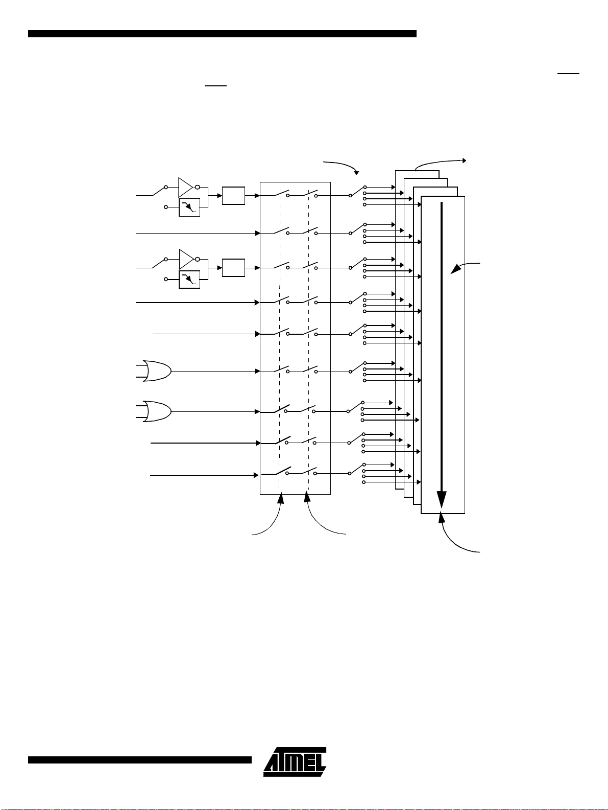
AT89C51RB2/RC2
om
Interrupt S yst em The A T89C51 RB2/RC2 has a tot al of 9 interrupt vectors: two external interrupts (INT0
and INT1), t hree timer i nterrupts ( timers 0, 1 a nd 2), the seria l port interr upt, SP I interrupt, Keyboard interrupt and the PCA global interrupt. These interrupts are shown in
Figure 22.
Figure 22. Interrupt Control System
IPH, IPL
High Priority
Interrupt
INT0
TF0
INT1
TF1
PCA IT
RI
TI
TF2
EXF2
KBD IT
SPI IT
IE0
IE1
3
0
3
0
3
0
3
0
3
0
3
0
3
0
3
0
3
0
Interrupt
Polling
Sequence, Decreasing Fr
High to Low Priority
4180E–8051–10/06
Individual Enable
Global Disable
Low Priority
Interrupt
Each of the interrupt sources can be individually enabled or disabled by setting or clearing a bit in t he Interrupt Enable regist er (Table 45 and Table 47). This register also
contains a global disable bit, which must be cleared to disable all interrupts at once.
Each interrupt source can also be individually programmed to one out of four priority levels by setting or clearing a bit in the Interrupt Priority register (Table 48) and in the
Interrupt Priority High register (Table 46 and Tabl e 47 ) s hows t he bit v alues an d priority
levels associated with each combination.
55
Page 56

AT89C51RB2/RC2
Registers A low-priority interrupt can be interrupted by a high-priority interrupt, but not by another
low-priority inte rrupt. A hig h-priori ty interrupt can’t be i nterrupte d by any ot her inte rrupt
source.
Table 43. Priority Level Bit Values
IPH. x IPL. x Interrupt Le ve l Prior ity
0 0 0 (Lowest)
011
102
113 (Highest)
If two interrupt requests of different priority levels are receiv ed simultaneously, th e
request of higher-priority level is serviced. If interrupt requests of the same priority level
are received simul taneous ly, an in terna l polling sequence determ ines wh ich requ est is
serviced. Thu s within ea ch priority l evel there i s a seco nd priority structure de termine d
by the polling sequence.
56
4180E–8051–10/06
Page 57

AT89C51RB2/RC2
Table 44. IENO Register
IEN0 - Interrupt Enable Register (A8h)
76543210
EA EC ET2 ES ET1 EX1 ET0 EX0
Bit
Number
7EA
6EC
5ET2
4ES
3ET1
2 EX1
1ET0
Bit
Mnemonic Description
Enable All Inter rupt Bit
Cleared to disable all interrupts.
Set to enable all interrupts.
PCA Interrupt Enable Bit
Cleared to disable.
Set to enable.
Timer 2 Overflow Interrupt Enable Bit
Cleared to disable timer 2 overflow interrupt.
Set to enable timer 2 overflow interrupt.
Serial Port Enable Bit
Cleared to disable serial port interrupt.
Set to enable serial port interrupt.
Timer 1 Overflow Interrupt Enable Bit
Cleared to disable timer 1 overflow interrupt.
Set to enable timer 1 overflow interrupt.
External Inter rup t 1 Enable Bit
Cleared to disable external interrupt 1.
Set to enable external interrupt 1.
Timer 0 Overflow Interrupt Enable Bit
Cleared to disable timer 0 overflow interrupt.
Set to enable timer 0 overflow interrupt.
0 EX0
External Inter rup t 0 Enable Bit
Cleared to disable external interrupt 0.
Set to enable external interrupt 0.
Reset Value = 0000 0000b
Bit addressable
4180E–8051–10/06
57
Page 58

AT89C51RB2/RC2
Table 45. IPL0 Register
IPL0 - Interrupt Priority Register (B8h)
76543210
- PPCL PT2L PSL PT1L PX1L PT0L PX0L
Bit
Number
7-
6 PPCL
5PT2L
4 PSL
3PT1L
2PX1L
1PT0L
0PX0L
Bit
Mnemonic Description
Reserved
The value read from this bit is indeterminate. Do not set this bit.
PCA Interrupt Priority Bit
see PPCH for priority level.
Timer 2 Overflow Interrupt Priority Bit
see PT2H for priority level.
Serial Port Priority Bit
see PSH for priority level.
Timer 1 Overflow Interrupt Priority Bit
see PT1H for priority level.
External Interrupt 1 Priority Bit
see PX1H for priority level.
Timer 0 Overflow Interrupt Priority Bit
see PT0H for priority level.
External Interrupt 0 Priority Bit
see PX0H for priority level.
Reset Value = X000 0000b
Bit addressable
58
4180E–8051–10/06
Page 59

AT89C51RB2/RC2
Table 46. IPH0 Register
IPH0 - Interrupt Priority High Register (B7h)
76543210
- PPCH PT2H PSH PT1H PX1H PT0H PX0H
Bit
Number
7-
6 PPCH
5PT2H
4 PSH
3PT1H
Bit
Mnemonic Description
Reserved
The value read from this bit is indeterminate. Do not set this bit.
PCA Interrupt Priority High Bit
PPCH
PPCL Priority Level
00Lowest
01
10
1 1 Highest
Timer 2 Overflow Interrupt Priority High Bit
PT2H
PT2L Priority Level
00Lowest
01
10
1 1 Highest
Serial Port Priority High Bit
PSH
PSL Priority Level
00Lowest
01
10
1 1 Highest
Timer 1 Overflow Interrupt Priority High Bit
PT1H
PT1L Priority Level
00Lowest
01
10
1 1 Highest
4180E–8051–10/06
External Interrupt 1 Priority High Bit
PX1H
2 PX1H
1PT0H
0 PX0H
00Lowest
01
10
1 1 Highest
Timer 0 Overflow Interrupt Priority High Bit
PT0H
00Lowest
01
10
1 1 Highest
External Interrupt 0 Priority High Bit
PX0H
00Lowest
01
10
1 1 Highest
Reset Value = X000 0000b
Not bit addressable
PX1L Priority Level
PT0L Priority Level
PX0L Priority Level
59
Page 60

AT89C51RB2/RC2
Table 47. IEN1 Register
IEN1 - Interrupt Enable Register (B1h)
76543210
-----ESPI-KBD
Bit
Number
7-Reserved
6-Reserved
5-Reserved
4-Reserved
3-Reserved
2ESPI
1-Reserved
0 KBD
Bit
Mnemonic Description
SPI Interrupt Enable Bit
Cleared to disable SPI interrupt.
Set to enable SPI interrupt.
Keyboard Interrupt Enable Bit
Cleared to disable keyboard interrupt.
Set to enable keyboard interrupt.
Reset Value = XXXX X000b
Bit addressable
60
4180E–8051–10/06
Page 61

AT89C51RB2/RC2
Table 48. IPL1 Register
IPL1 - Interrupt Priority Register (B2h)
76543210
- - - - - SPIL - KBDL
Bit
Number
7-
6-
5-
4-
3-
2 SPIL
1-
0 KBDL
Bit
Mnemonic Description
Reserved
The value read from this bit is indeterminate. Do not set this bit.
Reserved
The value read from this bit is indeterminate. Do not set this bit.
Reserved
The value read from this bit is indeterminate. Do not set this bit.
Reserved
The value read from this bit is indeterminate. Do not set this bit.
Reserved
The value read from this bit is indeterminate. Do not set this bit.
SPI Interrupt Priority Bit
see SPIH for priority level.
Reserved
The value read from this bit is indeterminate. Do not set this bit.
Keyboard Interrupt Priority Bit
see KBDH for priority level.
Reset Value = XXXX X000b
Bit addressable
4180E–8051–10/06
61
Page 62

AT89C51RB2/RC2
Table 49. IPH1 Register
IPH1 - Interrupt Priority High Register (B3h)
76543210
- - - - - SPIH - KBDH
Bit
Number
7-
6-
5-
4-
3-
2SPIH
1-
0 KBDH
Bit
Mnemonic Description
Reserved
The value read from this bit is indeterminate. Do not set this bit.
Reserved
The value read from this bit is indeterminate. Do not set this bit.
Reserved
The value read from this bit is indeterminate. Do not set this bit.
Reserved
The value read from this bit is indeterminate. Do not set this bit.
Reserved
The value read from this bit is indeterminate. Do not set this bit.
SPI Interrupt Priority High Bit
SPIH
SPIL Priority Level
00Lowest
01
10
1 1 Highest
Reserved
The value read from this bit is indeterminate. Do not set this bit.
Keyboard Interrupt Priority High Bit
KB DH
KBDL Priority Level
00Lowest
01
10
1 1 Highest
62
Reset Value = XXXX X000b
Not bit addressable
4180E–8051–10/06
Page 63

AT89C51RB2/RC2
Interrupt Sources and V ecto r Addr ess es
Table 50. Interrupt Sources and Vector Addresses
Number Polling Priority Interrupt Source
0 0 Reset 0000h
1 1 INT0 IE0 0003h
2 2 Timer 0 TF0 000Bh
3 3 INT1 IE1 0013h
4 4 Timer 1 IF1 001Bh
5 6 UART RI+TI 0023h
6 7 Timer 2 TF2+EXF2 002Bh
7 5 PCA CF + CCFn (n = 0-4) 0033h
8 8 Keyboard KBDIT 003Bh
9 9 SPI SPIIT 004Bh
Interrupt
Request
Vector
Address
4180E–8051–10/06
63
Page 64
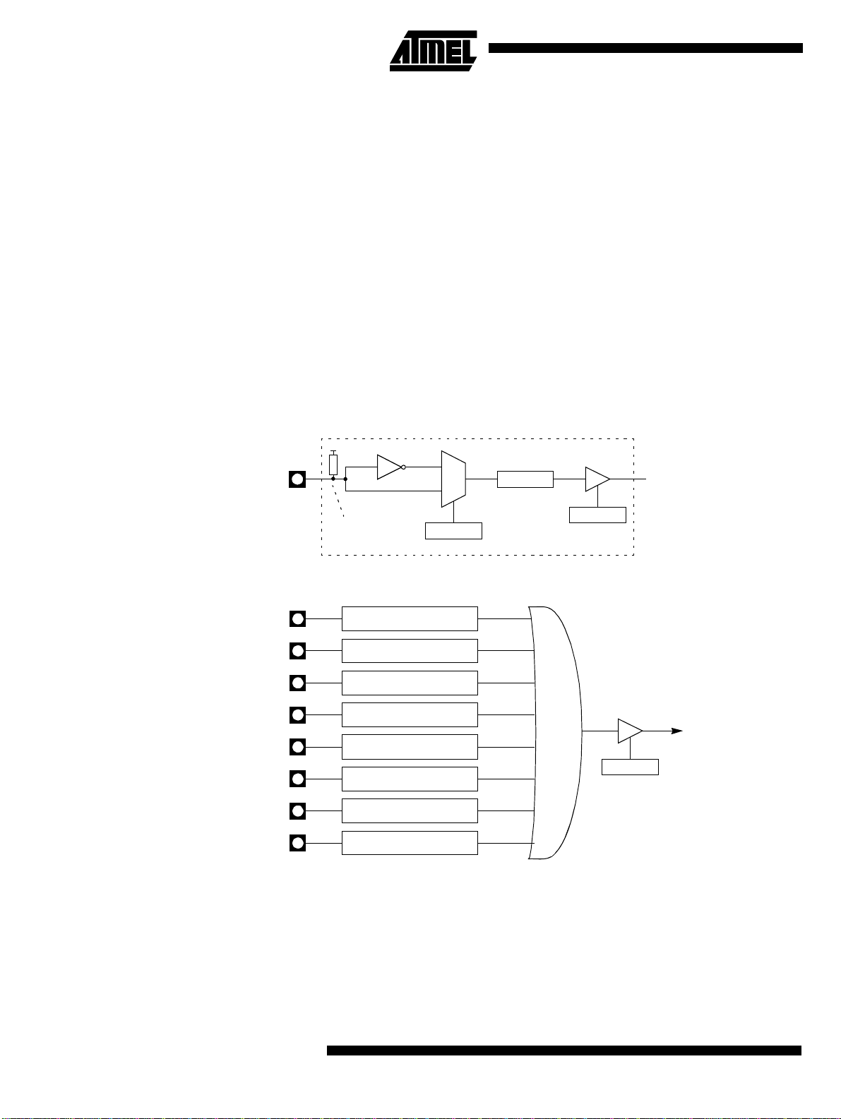
AT89C51RB2/RC2
Keyboard Interface The AT89C51RB2/RC2 implements a keyboard interface allowing the connection of a
P
8 x n matrix keyboard. It is based on 8 inputs with programmable interrupt capability on
both high or low level. These inputs are available as alternate function of P1 and allow to
exit from idle and power-down modes.
The keyboard interfaces with the C51 core through 3 spe cial function reg isters: KBLS,
the Keyboard Level Selection register (Table 5 3), KBE, the Keyboard interrupt Enable
register (Table 52 ), and KBF, the Keyboard Flag register (Table 51).
Interrupt The keyboard inputs are considered as 8 independent interrupt sources sharing the
same interrupt vector. An interrupt enable bit (KBD in IEN1) allows global enable or disable of the ke yboa rd interru pt (see F igure 23). As det ailed i n Figu re 24 each keyboa rd
input has the c apability to de tect a p rogrammab le level acc ordin g to KBLS . x bit value.
Level detection is then reported in interrupt flags KBF. x that can be masked by software
using KBE. x bits.
This structure allows keyboard arrangement from 1 by n to 8 by n matrix and allow
usage of P1 inputs for other purpose.
Figure 23. Keyboard Interface Block Diagram
V
CC
1:x
0
KBF. x
1
Internal Pull-up
KBLS. x
KBE. x
Figure 24. Keyboard Input Circuitry
P1.0
P1.1 Input Circuitry
P1.2 Input Circuitry
P1.3 Input Circuitry
P1.4 Input Circuitry
P1.5 Input Circuitry
P1.6 Input Circuitry
P1.7 Input Circuitry
Input Circuitry
KBD
IEN1
KBDIT
Keyboard Interface
Interrupt Request
Power Reduction Mode P 1 inputs allow exit from idle and power down modes as detailed in Section “Power-
down Mode”, page 82.
64
4180E–8051–10/06
Page 65

Registers Table 51. KBF Register
KBF - Keyboard Flag Register (9Eh)
76543210
KBF7 KBF6 KBF5 KBF4 KBF3 KBF2 KBF1 KBF0
AT89C51RB2/RC2
Bit
Number
7KBF7
6KBF6
5KBF5
4KBF4
3KBF3
2KBF2
Bit
Mnemonic Description
Keyboard Line 7 Flag
Set by har dwa re w he n the Port li ne 7 det e ct s a prog r ammed l ev el . It g ene rat e s a
Keyboard interrupt request if the KBKBIE. 7 bit in KBIE register is set.
Must be c leared by software .
Keyboard Line 6 Flag
Set by har dwa re w he n the Port li ne 6 det e ct s a prog r ammed l ev el . It g ene rat e s a
Keyboard interrupt request if the KBIE. 6 bit in KBIE register is set.
Must be c leared by software .
Keyboard Line 5 Flag
Set by har dwa re w he n the Port li ne 5 det e ct s a prog r ammed l ev el . It g ene rat e s a
Keyboard interrupt request if the KBIE. 5 bit in KBIE register is set.
Must be c leared by software .
Keyboard Line 4 Flag
Set by har dwa re w he n the Port li ne 4 det e ct s a prog r ammed l ev el . It g ene rat e s a
Keyboard interrupt request if the KBIE. 4 bit in KBIE register is set.
Must be c leared by software .
Keyboard Line 3 Flag
Set by har dwa re w he n the Port li ne 3 det e ct s a prog r ammed l ev el . It g ene rat e s a
Keyboard interrupt request if the KBIE. 3 bit in KBIE register is set.
Must be c leared by software .
Keyboard Line 2 Flag
Set by har dwa re w he n the Port li ne 2 det e ct s a prog r ammed l ev el . It g ene rat e s a
Keyboard interrupt request if the KBIE. 2 bit in KBIE register is set.
Must be c leared by software .
4180E–8051–10/06
Keyboard Line 1 Flag
1KBF1
0KBF0
Set by har dwa re w he n the Port li ne 1 det e ct s a prog r ammed l ev el . It g ene rat e s a
Keyboard interrupt request if the KBIE. 1 bit in KBIE register is set.
Must be c leared by software .
Keyboard Line 0 Flag
Set by har dwa re w he n the Port li ne 0 det e ct s a prog r ammed l ev el . It g ene rat e s a
Keyboard interrupt request if the KBIE. 0 bit in KBIE register is set.
Must be c leared by software .
Reset Value = 0000 0000b
This register is read only access , all flags are automatically cleared by readi ng the
register.
65
Page 66

AT89C51RB2/RC2
Table 52. KBE Register
KBE - Keyboard In p ut Enab le Register (9Dh)
76543210
KBE7 KBE6 KBE5 KBE4 KBE3 KBE2 KBE1 KBE0
Bit
Number
7 KBE7
6 KBE6
5 KBE5
4 KBE4
3 KBE3
2 KBE2
1 KBE1
Bit
Mnemonic Description
Keyboard Line 7 Enable Bit
Cleared to enable standard I/O pin.
Set to enable KBF. 7 bit in KBF register to generate an interrupt request.
Keyboard Line 6 Enable Bit
Cleared to enable standard I/O pin.
Set to enable KBF. 6 bit in KBF register to generate an interrupt request.
Keyboard Line 5 Enable Bit
Cleared to enable standard I/O pin.
Set to enable KBF. 5 bit in KBF register to generate an interrupt request.
Keyboard Line 4 Enable Bit
Cleared to enable standard I/O pin.
Set to enable KBF. 4 bit in KBF register to generate an interrupt request.
Keyboard Line 3 Enable Bit
Cleared to enable standard I/O pin.
Set to enable KBF. 3 bit in KBF register to generate an interrupt request.
Keyboard Line 2 Enable Bit
Cleared to enable standard I/O pin.
Set to enable KBF. 2 bit in KBF register to generate an interrupt request.
Keyboard Line 1 Enable Bit
Cleared to enable standard I/O pin.
Set to enable KBF. 1 bit in KBF register to generate an interrupt request.
0 KBE0
Keyboard Line 0 Enable Bit
Cleared to enable standard I/O pin.
Set to enable KBF. 0 bit in KBF register to generate an interrupt request.
Reset Value = 0000 0000b
66
4180E–8051–10/06
Page 67

AT89C51RB2/RC2
Table 53. KBLS Register
KBLS - Keyboard Level Selector Register (9Ch)
76543210
KBLS7 KBLS6 KBLS5 KBLS4 KBLS3 KBLS2 KBLS1 KBLS0
Bit
Number
7KBLS7
6KBLS6
5KBLS5
4KBLS4
3KBLS3
2KBLS2
1KBLS1
Bit
Mnemonic Description
Keyboard Line 7 Level Selection Bit
Cleared to enable a low level detection on Port line 7.
Set to enable a hi gh level detection on Port line 7.
Keyboard Line 6 Level Selection Bit
Cleared to enable a low level detection on Port line 6.
Set to enable a hi gh level detection on Port line 6.
Keyboard Line 5 Level Selection Bit
Cleared to enable a low level detection on Port line 5.
Set to enable a hi gh level detection on Port line 5.
Keyboard Line 4 Level Selection Bit
Cleared to enable a low level detection on Port line 4.
Set to enable a hi gh level detection on Port line 4.
Keyboard Line 3 Level Selection Bit
Cleared to enable a low level detection on Port line 3.
Set to enable a hi gh level detection on Port line 3.
Keyboard Line 2 Level Selection Bit
Cleared to enable a low level detection on Port line 2.
Set to enable a hi gh level detection on Port line 2.
Keyboard Line 1 Level Selection Bit
Cleared to enable a low level detection on Port line 1.
Set to enable a hi gh level detection on Port line 1.
0KBLS0
Keyboard Line 0 Level Selection Bit
Cleared to enable a low level detection on Port line 0.
Set to enable a hi gh level detection on Port line 0.
Reset Value = 0000 0000b
4180E–8051–10/06
67
Page 68
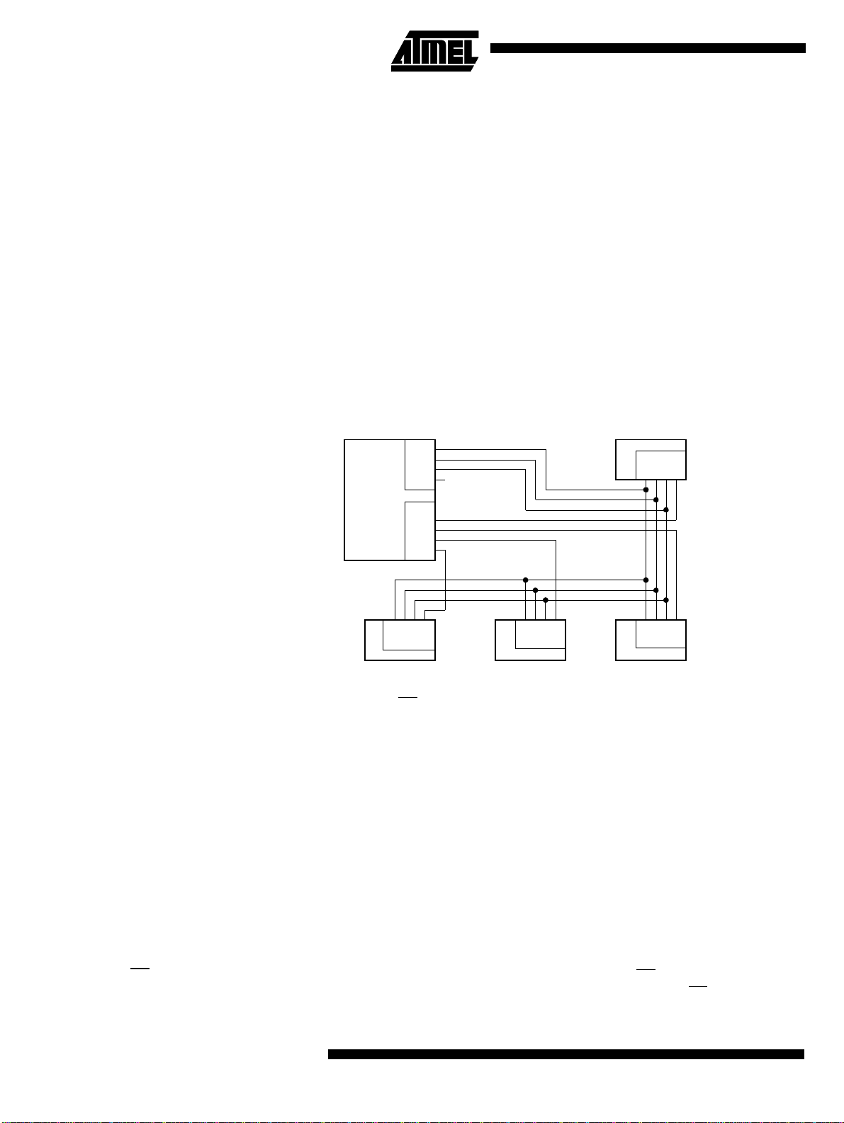
AT89C51RB2/RC2
Serial Port Interface (SPI)
The Serial Peripheral Interface Module (SPI) allows full-duplex, synchronous, serial
communication between the MCU and peripheral devices, including other MCUs.
Features Features of the SPI Module include the following:
• Full-duplex, three-wire synchronous transfers
• Master or Slave operation
• Eight programmable Master clock rates
• Serial clock with programma ble polarity and phase
• Master Mode fault error flag with MCU interrupt capability
• Writ e co llis ion flag prot ec ti o n
Signal Description Figure 25 shows a typical SPI bus configura tion usi ng one M aster con troller and m any
Slave peripherals. The bus is made of three wires connecting all the devices.
Figure 25. SPI Master/Slaves Interconnection
Master Output Slave Input
(MOSI)
Master Input Slave Output
(MISO)
MISO
MOSI
SCK
SS
VDD
Slave 1
MISO
MOSI
SCK
SS
Master
0
1
PORT
2
3
MISO
MOSI
SCK
MISO
MOSI
Slave 4
MISO
MOSI
SCK
SCK
SS
Slave 3
SS
SS
Slave 2
The Mast er de vi ce se lects the ind ivid ual S lave dev ices by u sin g fo ur pin s of a paral lel
port to control the four SS
pins of the Slave devices.
This 1-bit s igna l is direct ly conne cted b etwe en the Mast er Devi ce an d a Slave Devi ce.
The MOSI line is used to transfer data in series from the Master to the Slave. Therefore,
it is an output signal from the Master, and an input signal to a Slave. A Byte (8-bit word)
is transmitted most significant bit (MSB) first, least significant bit (LSB) last.
This 1-bit s ignal i s direct ly conne cted b etwe en the Slave De vice and a M aste r Device.
The MISO line is used to transfer data in series from the Slave to the Master. Therefore,
it is an output signal from the Slave, and an input signal to the Master. A Byte (8-bit
word) is transmitted most significant bit (MSB) first, least significant bit (LSB) last.
SPI Serial Clock (SCK) This signal is used to synchronize the data movement both in and out of the devices
through their MOSI and MISO lines. It is driven by the Master for eight clock cycles
which allows to exchange one Byte on the serial lines.
Slave Select (SS
) Each Slave peripheral is selected by one Slave Select pin (SS). This signal m ust stay
low for any message for a S lave. It is obvious t hat only one M aster (SS
high level) can
68
4180E–8051–10/06
Page 69

AT89C51RB2/RC2
drive the network. The Master may select each Slave device by software through port
pins (Figure 26). To prevent bus conflicts on the MISO line, only one slave should be
selected at a time by the Master for a transmission.
In a Master co nfiguration, t he S S
line can be us ed i n conj unc tion wi th the M ODF flag i n
the SPI Status register (SPSTA) to prevent multiple masters from driving MOSI and
SCK (see Error conditions).
A high level on the SS
The SS
pin could be used as a general-purpose if the following conditions are met:
pin puts the MISO line of a Slave SPI in a high-impedance state.
• The device is configured as a Master and the SSDIS control bit in SPCON is set.
This kind of configuration can be found when only one Master is driving the network
and there is no way that the SS
the SPSTA will never be set
• The Device is configured as a Slave with CPHA and SSDIS control bits set
pin could be pulled low. Therefore, the MODF flag in
(1)
.
(2)
. This
kind of configuration can happen when the system comprises one Master and one
Slave only. Therefore, the device should always be selected and there is no reason
that the Master uses the SS
Note: 1. Clearing SSDIS control bit does not clear MO DF.
2. Special care should be taken not to set SSDIS control bit when CPHA = ’0’ because
in this mode, the SS
pin to select the communicating Slave device.
is used to start the tr ansm ission.
Baud Rate In Master mode, the baud rate can be selected from a baud rate generator which is con-
trolled by three bits in the SPCON register: SPR2, SPR1 and SPR0.The Master clock is
selected from one of seven clock rates resulting from the division of the internal clock by
2, 4, 8, 16, 32, 64 or 128.
Table 54 gives the different clock rates selected by SPR2:SPR1:SPR0.
Table 54. SPI Master Baud Rate Selection
SPR2 SPR1 SPR0 Clock Rate Baud Rate Divisor (BD)
000 F
001 F
010 F
011 F
100 F
101 F
110 F
1 1 1 D on’t Use No BRG
CLK PERIPH
CLK PERIPH
CLK PERIPH
CLK PERIPH
CLK PERIPH
CLK PERIPH
CLK PER IP H
/2 2
/4 4
/8 8
/16 16
/32 32
/64 64
/128 128
4180E–8051–10/06
69
Page 70
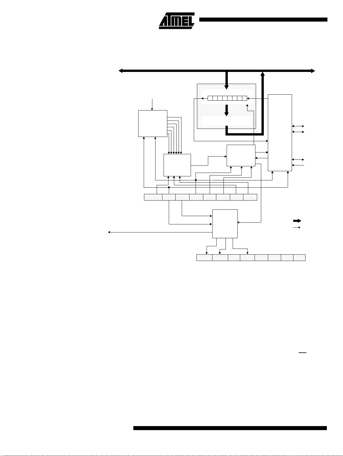
AT89C51RB2/RC2
Functional Description Figure 26 shows a detailed structure of the SPI Module.
l
Figure 26. SPI Module Block Diagram
Internal Bus
SPDAT
FCLK PERIPH
Clock
Divider
SPR2
SPI Interrupt Request
/128
/8
/16
/32
/64
/4
Clock
Select
Shift R e gi s te r
234567
01
Receive Data Register
Clock
Logic
CPHA SPR0SPR1CPOLMSTRSSDISSPEN
SPCON
SPI
Control
WCOL MODFSPIF
-----
Pin
Control
Logic
M
S
MOSI
MISO
SCK
SS
8-bit bus
1-bit signa
SPSTA
Operating Modes The Serial Peripheral Interface can be configured in on e of the two mod es: Master
mode or Slave mode. The configuration and initialization of the SPI Module is made
through one register:
• The Serial Peripheral Control register (SPCON)
Once the SPI is configured, the data exchange is made using:
•SPCON
• The Serial Peripheral STAtus register (SPSTA)
• The Serial Peripheral DATa register (SPDAT)
During an SPI transmission, data is simultaneous ly transmitte d (shifted ou t serially) and
received (shifted in serially). A serial clock line (SCK) synchronizes shifting and sampling on the two serial data lines (MOSI and MISO). A Slave Select line (SS
) allows
individual selection of a Slave SPI device; Slave devices that are not selected do not
interfere with SPI bus activities.
When the Master device transmits data to the Slave device via the MOS I line, the Slave
device responds by sending data to the Master device via the MISO line. This implies
full-duplex transmission with both data out and data in synchronized with the same clock
(Figure 27).
70
4180E–8051–10/06
Page 71

Figure 27. Full-Duplex Master-Slave Interconnection
AT89C51RB2/RC2
MISOMISO
MOSI
VSS
8-bit Shift register
SSSS
Slave MCU
SPI
Clock Generator
Master MCU
8-bit Shift register
MOSI
SCK SCK
VDD
Master Mo de The SPI operates in Master mode when the Master bit, MSTR
is set. Only one Master SPI device can initiate transmissions. Software begins the transmission from a Master SPI Module by writing to the Serial Peripheral Data Register
(SPDAT). If the shift reg ister is e mpty, th e Byte i s immedia tely tra nsferred to the sh ift
register. The Byte begi ns shifting out on M OSI pin under the con trol of the serial clock,
SCK. S imultan eou sly, a nother B yte shifts i n fro m the S lave on th e Mas ter’s MISO pi n.
The transmission ends w hen the Se rial Periphera l transfer da ta flag, SPIF , in SPSTA
becomes set. At the same time that SPIF becomes set, the received Byte from the Slave
is tran sfe rred t o th e recei ve data re giste r in S PDA T. Soft war e c lear s SPI F by r eadin g
the Serial Peripheral Status register (SPSTA) with the SPIF bit set, and then reading the
SPDAT.
Slave Mode The SPI operates in Slave mode when the Master bit, MSTR
(2)
cleared. Bef ore a data tran smission occu rs, the Slave Select pin, SS
device must be set to ’0’. SS
must remain low until the transmission is complete.
In a Slave SPI Mod ule, da ta enters the s hift registe r under th e control of the S CK from
the Master SPI Module. After a Byte enters the shift register, it is immediately transferred to the receive data register in SPDAT, and the SPIF bit is set. To prevent an
overflow condition, Slav e software must then read the SPDAT before anothe r Byte
enters the shift register
(3)
. A Slave SPI must complete the write to the SPDAT (shift register) at least one bus cycle before the Master SPI starts a transmission. If the write to
the data register is late, the SPI transmits the dat a already in the shift reg ister from the
previous transmission. The maximum SCK frequency allowed in slave mode is
/4.
(1)
, in the SPCON register
, in the SPCON register is
, of the Slave
F
CLK PERIPH
Transmission Formats Software c an selec t any of fo ur c omb inati ons of seri al cl ock ( SCK) ph ase an d p olar ity
using two bits in the SPCON: the Clock Polarity (CPOL
(CPHA
4
). CPOL defines the default SCK line level in idle state. It has no significant
(4)
) and the Clock Phase
effect on the transmission format. CPHA defines the edges on which the input data are
sampled and the edges on which the output data are shifted (Figure 28 and Figure 29).
The clock phase and polarity should be identical for the Master SPI device and the communicating Slave device.
1. The SPI Module should be configured as a Master before it is enabled (SPEN set). Also,
the Master SPI should be confi gured before the Slave SPI.
2. The SPI Module should be configured as a Slav e before it is enabled (SPEN set).
3. The maximum frequency of the SCK for an SPI configured as a Slave is the bus clock
speed.
4. Before writing to the CPOL and CPHA bits, the SPI should be disabl ed (SPEN = ’0’).
71
4180E–8051–10/06
Page 72
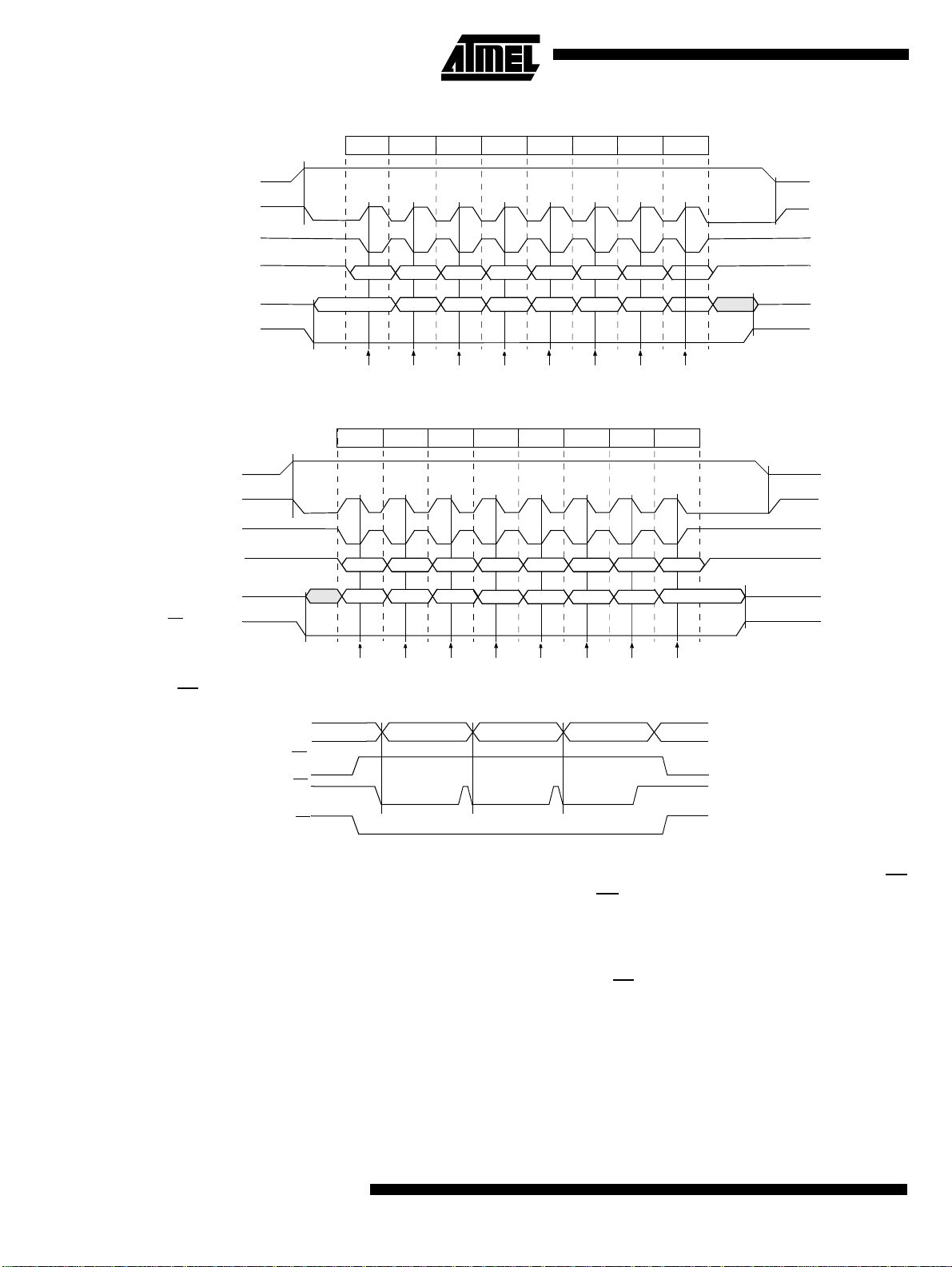
AT89C51RB2/RC2
Figure 28. Data Transmission Format (CPHA = 0)
SCK Cycle Number
SPEN (Internal)
SCK (CPOL = 0)
SCK (CPOL = 1)
132 45678
MOSI (from Master)
MISO (from Sla ve)
SS (to Slave)
Capture Point
MSB bit6 bit5 bit4 bit3 bit2 bit1 LSB
Figure 29. Data Transmission Format (CPHA = 1)
SCK Cycle Number
SPEN (Internal)
SCK (CPOL = 0)
SCK (CPOL = 1)
MOSI (from Master)
MISO (from Slave)
SS
(to Slave)
Capture Point
Figure 30. CPHA/SS
Timin g
MISO/MOSI
132 45678
MSB bit6 bit5 bit4 bit3 bit2 bit1 LSB
MSB LSB
bit6 bit5 bit4 bit3 bit2 bit1MSB
bit6 bit5 bit4 bit3 bit2 bit1
Byte 1 Byte 2
Byte 3
LSB
72
Master SS
Slave SS
(CPHA = 0)
Slave SS
(CPHA = 1)
As shown in Figure 28, the first SCK edge is the MSB capture strobe. Therefore, the
Slave must begin driving its data before the first SCK edge, and a falling edge on the SS
pin is used to start the transmission. The SS pin must be toggled high and then low
between each Byte transmitted (Figure 30).
Figure 29 shows an SPI transmission in which CPHA is ’1’. In this case, the Master
begins driving its MOSI pin on the first SCK edge. Therefore, the Slave uses the first
SCK edge as a start transmission signal. The SS
pin can remain low between transmissions (Figure 30). This format may be preffered in systems having only one Master and
only one Slave driving the MISO data line.
4180E–8051–10/06
Page 73

AT89C51RB2/RC2
Error Conditions The following flags in the SPSTA signal SPI error conditions:
Mode Fault (MODF) Mode Fault e rror in Ma ster m ode S PI indi cate s that t he le vel on the Sl ave S elect (S S
pin is inconsistent with the actua l mode of th e device. MO DF is set to warn th at there
may be a multi-master conflict for system control. In this case, the SPI system is
affected in the following ways:
• An SPI receiver/error CPU interrupt request is generated
• The SP EN bit in SPCON is cleared. This disables the SPI
• The MST R bit in SPCON is cleared
When SS
when the SS
However, as stated before, for a system with one Master, if the SS
Disable (SSDIS) bit in the SPCON register is cleared, the MODF flag is set
signal becomes ’0’.
pin of the Master
device is pulled low, there is no way that another Master attemp ts to drive the network.
In this case, to prevent the MODF flag from being set, software can set the SSD IS bit in
the SPCON register and therefore making the SS
pin as a general-purpose I/O pin.
Clearing the MODF bit is accomplished b y a read of SPSTA regi s ter with MODF bit s et,
followed by a write to the SPCON register. SPEN Control bit may be restored to its original set state after the MODF bit has been cleared.
Write Collis ion (WCOL) A Write Collision (WCOL) flag in the SPSTA is set when a write to the SPDAT register is
done during a transmit sequence.
WCOL does not cause an interruption, and the transfer continues uninterrupted.
Clearing the WCOL bit is done through a software sequence of an access to SPSTA
and an access to SPDAT.
)
Overrun Condition A n ove rrun co ndition occu rs when the M aster device tries to send s evera l data Byte s
and the Slave devise has not cleared the SPIF bit issuing from the previous data Byte
transmitted. In this case, the receiver buffer contains the Byte sent after the SPIF bit was
last cleared. A read of the SPDAT returns this Byte. All others Bytes are lost.
This condition is not detected by the SPI peripheral.
SS Error Flag (SSERR) A Synchronous Serial Slave Error occurs when SS
goes high before the end of a
received data in sl ave m ode. SSERR d oes n ot cau se in i nterrupt ion, thi s bit is c leare d
by writing 0 to SPEN bit (reset of the SPI state machine).
Interrupts Two SPI status flags can generate a CPU interrupt requests:
Table 55. SPI Interru p ts
Flag Request
SPIF (SP data transfer) SPI Transmitter Interrupt request
MODF (Mode Fault) SPI Receiver/Error Interrupt Request (if SSDIS = ’0’)
Serial Peripheral data transfer flag, SPIF: This bit is set by hardware when a transfer
has been completed. SPIF bit generates transmitter CPU interrupt requests.
Mode Fault flag, MODF: This bit becomes set to indicate that the level on the SS is
inconsistent with the mode of the SPI. MODF with SSDIS reset, generates receiver/error
CPU interrupt requests. When SSDIS is set, no MODF interrupt request is generated.
4180E–8051–10/06
Figure 31 gives a logical view of the above statements.
73
Page 74

AT89C51RB2/RC2
Figure 31. SPI Interrupt Requests Generation
Registers
Serial Peripheral Control
Register (SPCON)
SPIF
MODF
SSDIS
There are three registers in the Module that provide control, status and data storage functions. These registers
are desc r i be s in the followi ng par ag raphs.
SPI Transmitter
CPU Interrupt Request
SPI Receiver/error
CPU Interrupt Request
SPI
CPU Interrupt Request
• The Serial Peripheral Control Register does the following:
• Se lects one of the Master clock rates
• Conf igure the SPI Module as Master or Slave
• Selects serial clock polarity and phase
• En ables the SPI Module
• Frees the SS pin for a general-purpose
Table 56 describes this register and explains the use of each bit
Table 56. SPCON Register
SPCON - Serial Peripheral Control Register (0C3H)
76543210
SPR2 SPEN SSDIS MSTR CPOL CPHA SPR1 SPR0
Bit Number Bit Mnemonic Description
7 SPR2
6 SPEN
5SSDIS
4MSTR
3CPOL
2CPHA
Serial Peripheral Rate 2
Bit with SPR1 and SPR0 define the clock rate.
Serial Peripheral Enable
Cleared to disable the SPI interface.
Set to enable th e SPI interface.
Disable
SS
Cleared to enable SS
Set to disable SS
this bit has no effect if CPHA =’0’. When SSDIS is set, no MODF
interrupt request is generated
Seria l Peripher al Master
Cleared to configure the SPI as a Sla v e.
Set to configure the SPI as a Master.
Clock Polarity
Cleared to have the SCK set to ’0’ in idle state.
Set to have the SCK set to ’1’ in idle low.
Clock Phase
Cleared to have the data s ampled when the SCK l eaves the idle
state (see CPOL).
Set to h ave the dat a sa mp le d wh en th e SCK r etur ns t o i dl e s tat e (s ee
CPOL).
in both Master and Slave modes.
in both Master and Slave modes. In Slave mode,
.
74
4180E–8051–10/06
Page 75

Bit Number Bit Mnemonic Description
SPR2
SPR1 SPR0 Serial Peripheral Rate
1
0 SPR0
SPR1
00 0F
00 1 F
01 0 F
01 1F
10 0F
10 1F
11 0F
1 1 1 Invalid
Reset Value = 0001 0100b
Not bit addressable
AT89C51RB2/RC2
CLK PERIPH
CLK PERIPH
CLK PERIPH
CLK PERIPH
CLK PERIPH
CLK PERIPH
CLK PERIPH
/2
/4
/8
/16
/32
/64
/128
Serial Peripheral Status Register
(SPSTA)
The Serial Peripheral Status Register contains flags to signal the following conditions:
• Data transfer complete
• Writ e co llis ion
• Inconsi stent logic level on SS
pin (mode fault error)
Table 57 describes the SPSTA register and explains the use of every bit in the register.
Table 57. SPSTA Register
SPSTA - Serial Peripheral Status and Control register (0C4H)
76543210
SPIF WCOL SSERR MODF - - - -
Bit
Number
7 SPIF
6WCOL
Bit
Mnemonic Description
Serial Peripheral Data Transfer Flag
Cleared by hardware to indicate data transfer is in progress or has been
approved by a clearing sequence.
Set by hardware to indicate that the data transfer has been completed.
Write Collision Flag
Cleared by hardw are to indicate th at no collision has occurred or has been
approved by a clearing sequence.
Set by hardware to indicate that a collision has been detected.
4180E–8051–10/06
Synchronous Serial Slave Error Flag
5 SSERR
4MODF
3-
2-
Set by hardware when SS
Cleared by disabling the SPI (clearing SPEN bit in SPCON).
Mode Fault
Cleared by hardware to indicate that the SS
has been approved by a clearing sequence.
Set by hardware to indicate that the SS
Reserved
The valu e read from thi s bit is ind et er m in at e. Do not set this bit
Reserved
The valu e read from thi s bit is ind et er m in at e. Do not set this bit.
is deasse rted before the end of a received data .
pin is at appropriate logic level, or
pin is at inappropriate logic level.
75
Page 76

AT89C51RB2/RC2
Bit
Number
Bit
Mnemonic Description
Serial Peripheral DATa Register
(SPDAT)
1-
0-
Reserved
The valu e read from thi s bit is ind et er m in at e. Do not set this bit.
Reserved
The valu e read from thi s bit is ind et er m in at e. Do not set this bit.
Reset Value = 00X0 XXXXb
Not Bit addressable
The Serial Peripheral Data Register (Table 58) is a read/write buffer for the receive data
register. A write to SPDAT places data directly into the shift register. No transmit buff er i s
available in this model.
A Read of the SPDAT returns the value located in the receive buffer and not the content
of the shift register.
Table 58. SPDAT Register
SPDAT - Serial Peripheral Data Register (0C5H)
76543210
R7 R6 R5 R4 R3 R2 R1 R0
Reset Valu e = In determinate
R7:R0: Receive data bits
SPCON, SPSTA and SPD AT registers may be read and written at any time while there
is no on-going ex chang e. Howeve r, spec ial care sh ould be take n whe n writing to them
while a transmission is on-going:
• Do not change SP R2, SP R1 and SPR0
• Do not change CPHA and CPOL
• Do not change M STR
• Clearing SPEN would immediately disable the per ipheral
• Writing to the SPDAT will cause an overflow.
76
4180E–8051–10/06
Page 77

AT89C51RB2/RC2
Hardware Watchdog Timer
The WDT is intended as a recovery method in situations where the CPU may be subjected to software upset. The WDT consists of a 14-bit counter and the Watchdog Timer
Reset (WDTRST) SFR. The WDT is by default disabled from exiting reset. To enable
the WDT, user m ust write 01 EH and 0 E1H in se quence t o the WD TRST, S FR locatio n
0A6H. When WDT is enab led, it will increment every machine cycle while the oscillator
is running and there is no way to disable the WDT except through reset (either hardware
reset or WDT overflow reset). When WDT overflows, it will drive an output RESET HIGH
puls e at the RST -pin.
Using the WDT To enable the WDT, user must write 01EH and 0E1H in sequence to the WDTRST, SFR
location 0A6H. When WDT is enabled, the user needs to service it by writing to 01EH
and 0E1H to WDTRST to avoid WDT overflow. The 14-bit counter overflows when it
reaches 16383 (3FFFH) and this will reset the device. When WDT is enabled, it will
increment every machine cycle while the oscillator is running. This means the user must
reset the WDT at least every 16383 machine cycle. To reset the WDT the user must
write 01EH and 0E1H to WDT RST . WDT R ST is a write only reg ister. Th e WDT count er
cannot be read or written. When WDT overflows, it will generate an output RESET pulse
at the RST-pin. The RESET pulse duration is 96 x T
. To make the best use of the WDT, it should be serviced in those sections of code
PERIPH
CLK PER IPH
that will periodically be executed within the time required to prevent a WDT reset.
7
To have a more powerful WDT, a 2
capability , rank ing fro m 16 ms to 2 s @ F
counter has been added to extend the Time-out
= 12 MHz. T o ma na ge this f eat ure, se e
OSCA
WDTPRG register description, Table 59.
, where T
CLK PERIPH
= 1/F
CLK
Table 59. WDTRST Register
WDTRST - Watchdog Reset Register (0A6h)
76543210
--------
Reset Value = XXXX XXXXb
Write only, this SFR is used to reset/enable the WDT by writing 01EH then 0E1H in
sequence.
4180E–8051–10/06
77
Page 78

AT89C51RB2/RC2
Table 60. WDTPRG Register
WDTPRG - Watchdog Timer Out Register (0A7h)
76543210
- - - - - S2 S1 S0
Bit
Number
765432S2WDT Time-out Select Bit 2
1S1WDT Time-out Select Bit 1
0S0WDT Time-out Select Bit 0
Bit
Mnemonic Description
Reserved
The value read from this bit is undetermined. Do not try to set this bit.
S2
S1 S0Selected Time-out
000(2
001(2
010 (2
011(2
100(2
101 (2
110(2
111 (2
Reset Value = XXXX X000
14
- 1) machin e cy c les , 16. 3 ms @ F
15
- 1) machin e cy c les , 32.7 ms @ F
16
- 1) machin e cycles, 65. 5 ms @ F
17
- 1) machine cycles, 131 ms @ F
18
- 1) machine cycles, 262 ms @ F
19
- 1) machine cycles, 542 ms @ F
20
- 1) machin e cy c les , 1. 0 5 s @ F
21
- 1) machine cycles, 2 .09 s @ F
OSCA
OSCA
OSCA
OSCA
OSCA
OSCA
OSCA
OSCA
= 12 MHz
= 12 MHz
= 12 MHz
= 12 MHz
= 12 MHz
= 12 MHz
= 12 MHz
= 12 MHz
WDT During Power-down and Idle
78
In Powe r- down mo de t he osc illato r s tops , wh ich mea ns the WDT al so s tops. Wh ile in
Power-down mode the user does not need to service the WDT. There are two m et hods
of exiting Power-down mode: by a hardware reset or via a level activated external interrupt which is enabled prior to entering Power-down mode. When Power-down is exited
with hardware reset, servicing the WDT should occur as it normally should whenever the
AT89C51 RB2/RC 2 is reset. Exiting P ower-d own with a n interru pt is signi ficant ly different. The interrupt is held low long enough for the oscillator to stabilize. When the
interrupt is brought high, the interrupt is serviced. To prevent the WDT from resetting the
device while the interrupt pin is held low, the WDT is not started until the interrupt is
pulled high. It is suggested that the WDT be reset during the interrupt service routine.
To ensure that the WDT does not overflow within a few states of exiting of power-down,
it is better to reset the WDT just before entering power-down.
In the Idle mode, the oscillator co ntinues to run. To preven t the WDT from resetting t he
AT89C51RB2/RC2 while in Idle mode, the user should always set up a timer that will
periodically exit Idle, service the WDT, and re-enter Idle mode.
4180E–8051–10/06
Page 79

AT89C51RB2/RC2
ONCE™ Mode (O N Chip Emulation)
The ONCE mode facilitates testing and debugging of systems using AT89C51RB2/RC2
without removing the circuit f rom the board. The ONCE m ode is i nv oked b y driving certain pins of the AT89C51RB2/RC2; the following sequence must be exercised:
• Pull ALE low while the device is in reset (RST high) and PSEN
• Hold ALE low as RST is deactivated.
While the AT89C51RB2/RC2 is in ONCE mode, an emulator or test CPU can be used to
drive the circuit. Table 61 shows the status of the port pins during ONCE mode.
Normal operation is restored when normal reset is applied.
Table 61. External Pin Status during ONCE Mode
ALE PSEN Port 0 Port 1 Port 2 Port 3 XTAL1/2
Weak pull-up Weak pull-up Float Weak pull-up Weak pull-up Weak pull-up Active
is high.
4180E–8051–10/06
79
Page 80

AT89C51RB2/RC2
Power Mana gement Two powe r reduction modes are implemented in the AT89C51RB2/RC2: th e Idle mode
and the Power-down mode. These modes are detailed in the following sections. In addition to these power reduction modes, the clocks of the core and peripherals can be
dynamically divided by 2 using the X2 mode detailed in Section “X2 Feature”.
Reset In order to start-up (cold reset) or to restart (warm reset) properly the microcontroller, an
high level has to be applied on the RST pin. A bad level leads to a wrong initialization of
the internal registers like SFRs, Program Counter… and to unpredictable behavior of
the microcontroller. A proper device reset initializes the AT89C51RB2/RC2 and vectors
the CPU to add ress 0000h. RST in put has a pull-down resistor allowing po wer-on reset
by simply conn ec ting an ex ternal ca pacitor t o V
can be applied either directly on the RST pin or indirectly by an internal reset source
such as the watchdog timer. Resistor value and input characteristics are discussed in
the Section “DC Characteristics” of the AT89C51RB2/RC2 datasheet.
Figure 32. Reset Circuitry and Power-On Reset
VDD
P
RST
RST
R
VSS
as shown in Figure 32. A warm reset
DD
From Internal
Reset Source
To CPU Core
and Peripherals
VDD
+
RST
Cold Reset 2 conditions are required before enabling a CPU start-up:
•V
must reach the specified VDD range
DD
• The level on X1 input pin must be outside the specification (V
If one of these 2 conditions are not met, the microcontroller does not start correctly and
can exe cu te a n ins truc tion f etc h fr om any wh ere in th e prog ra m sp ace . An acti ve le vel
applied on the R ST pin mu st be maintain ed till both of the above con ditions are m et. A
reset is active when the level V
period of time where V
and the oscillator are n ot stabilize d. 2 parameters have to be
DD
is reached and when the p ulse width covers th e
IH1
taken into account to determine the reset pulse width:
•V
rise time,
DD
• O s c illator startup time.
To determine the capacitor value to implement, the highest value of these 2 parameters
has to be chosen. Table 1 gives some capacitor values examples for a minimum R
50 KΩ and different oscillator startup and V
rise times.
DD
Power-on ResetRST inpu t c ircui try
IH
, VIL)
RST
of
80
4180E–8051–10/06
Page 81
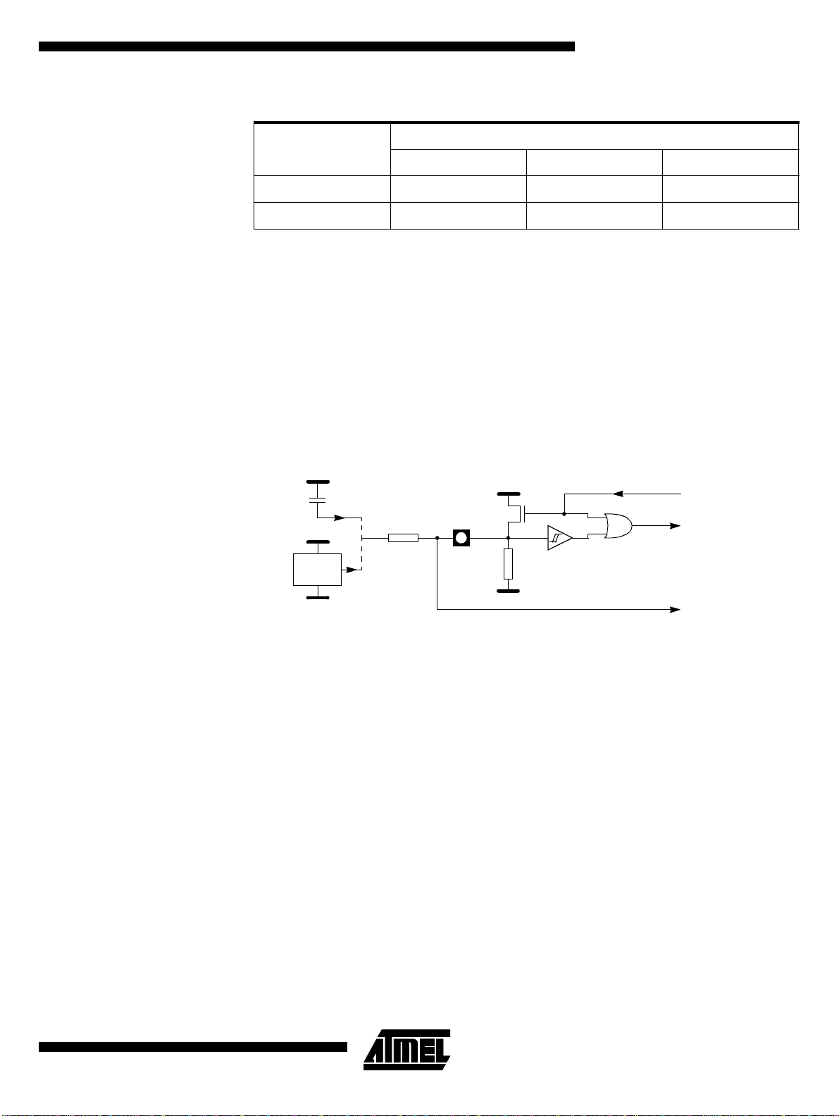
AT89C51RB2/RC2
Table 1. Minimum Reset Capacitor Value for a 50 kΩ Pull-down Resistor
(1)
VDD Rise Time
Oscillator
Start-Up Time
1 ms 10 ms 100 ms
5 ms 820 nF 1.2 µF 12 µF
20 ms 2.7 µF 3.9 µF 12 µF
Note: These values assume VDD starts from 0V to the nominal value. If the time between 2
on/off sequences is too fast, the power-supply de-coupling capacitors may not be fully
discharged, le ading to a bad reset sequence.
Warm Reset To achieve a valid reset, the reset signal must be maintained for at least 2 machine
cycles (24 o scil lator cl ock p eriods) w hile the o scillato r is runn ing. Th e n umber of clock
periods is mode independent (X2 or X1).
Watchdog Reset As detailed in Section “Hardware Watchdo g Timer”, page 77, the WDT generates a 96-
clock period pulse on the RST pin. In order to properly propagate this pulse to the rest of
the appl ication in case of ext ernal capac itor or pow er-supp ly su perv isor circ uit, a 1 kΩ
resistor must be added as shown Figure 33.
Figure 33. Reset Circuitry for WDT Reset-out Usage
VDD
VDD
+
RST
1K
VDD
From WDT
Reset Source
P
To CPU Core
and Peripherals
VSS
RST
VSS
RST
R
To Other
On-board
Circuitry
4180E–8051–10/06
81
Page 82

AT89C51RB2/RC2
Reset Recommendation to Prevent Flash Corruption
An example of bad initialization situation may occur in an instance where the bit
ENBOOT in AUXR1 register is initialized from the hardwa re bit BLJB upon reset. Since
this bit allows mapping of the bootloader in the code area, a reset failure can be critical.
If one w ants th e EN BOOT cleare d in o rde r to unm ap t he boo t from the code a rea (yet
due to a bad reset) the bit ENBOOT in SFRs may be set. If the value of Program
Counter i s ac cidentl y in t he ran ge of the boo t m emory addres ses t hen a Flash acc ess
(write or erase) may corrupt the Flash on-chip memory.
It is recommended to use an external reset circuitry featuring power supply monitoring to
prevent system malfunction during periods of insufficient pow er supply voltage (p ower
supply failure, power supply switched off).
Idle Mode An instruction that sets PCON.0 indicates that it is the last instruction to be executed
before going into Idle mode. In Idle mode, the internal clock signal is gated off to the
CPU, but not t o the i nterrup t, Ti mer, a nd Seri al Po rt func tion s. The CPU status is pr eserved in its entirety: th e Stack Pointer , Program Coun ter, Program Status W ord,
Accumulator and all other registers maintain their data during idle. The port pins hold the
logical states they had at the time Idle was activated. AL E and PSEN hold at logic high
level.
There are tw o ways to t erminat e the I dle mode. Activa tion of a ny enabl ed interru pt will
cause PCON.0 to be cleared by hardware, termi nating the Idle mode . The interrupt will
be serviced , and fol lowin g RETI th e next ins tructio n to be ex ecut ed will be the one following the instruction that put the device into idle.
The flag bits GF0 and GF1 can be used to give an indication if an interrupt occurred during normal operation or during idle. For example, an instruction that activates idle can
also set one or both flag bits . When idle is terminated by an interrupt, the interrupt service routine can examine the flag bits.
The other way of terminating the Idle mode is with a hardware reset. Since the clock
oscillator is still running, the hardware reset needs to be held active for only two
machine cycles (24 oscillato r p e riods ) to co mplete the reset.
Power-down Mode To save maximum power, a Power-do wn mode can be invoked by software (see Table
14, PCON register).
In Power-down mode, the os cillator is stopped a nd the instructi on tha t invoked P ower-
down mode is the last instruction executed. The internal RAM and SFRs retain their
value until the Power-down mode is terminated. V
power. Eith er a ha rdwa re reset o r an exte rnal interru pt ca n ca use an e xit fro m Powe rdown. To pr operly terminat e Pow er-down, t he reset or ext ernal interr upt sho uld no t be
executed before V
long enough for the oscillator to res ta rt and stabi liz e.
Only external interrupts INT0
Power-down. For that, interrupt must be enabled and c onfigured as level or edge s ensitive interrupt input. When Keyboard Interrupt occurs after a power down mode, 1024
clocks are necessary to exit to power down mode and enter in operating mode.
Holding the pin low restarts the oscillator but bringing the pi n high com pl etes the exit as
detailed in F igure 34. W hen both interrupt s are ena bled, the oscilla tor restart s as soon
as one of the two inputs is held low and power down exit will be completed when the first
input will be released. In this case, the higher priority interrupt service routine is executed. Once the interrupt is serviced, the next instruction to be executed after RETI will
is restored to its normal operating level and must be held active
CC
, INT1 and Keyboard Interrupts are useful to exit from
can be lowered to save further
CC
82
4180E–8051–10/06
Page 83
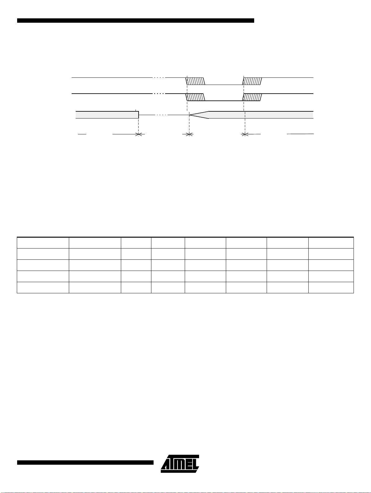
be the one following the instruction that puts the AT89C51RB2/RC2 into Power-down
mode.
Figure 34. Power-down Exit Waveform
INT0
INT1
XTALA
or
XTALB
Exit from Power-d own by reset re defines all the SFRs , exit from Power-down by external interrupt does no affect the SFRs.
Exit from Power-down by either reset or external interrupt or keyboard interrupt does not
affect the inter n al RAM cont en t.
Note: If idle mode is activated with Power-down mode (IDL and PD bits set), the exit sequen ce
AT89C51RB2/RC2
Power-down Phase Oscillator Restart Phase Active PhaseActive Phase
is unchanged, when execution is vectored to interrupt, PD and IDL bits are cleared and
idle mode is not entered.
Table 62 shows the state of ports during idle and power-down modes.
Table 62. State of Ports
Mode Program Memory ALE PSEN PORT0 PORT1 PORT2 PORT3
Idle Internal 1 1 Port Data
Idle Exte r nal 1 1 Float ing P ort D ata Address Port Data
Power Down Internal 0 0 Port Data
Power Down Exte rnal 0 0 Floating Port Data Port Data Port Data
Port 0 can force a 0 level. A "one" will leav e port floating.
(1)
(1)
Port Data Port Data P ort Data
Port Data Port Data P ort Data
4180E–8051–10/06
83
Page 84

AT89C51RB2/RC2
Power-off Flag The Power-off flag allows the user to distinguish between a “cold start” reset and a
“warm start” reset.
A cold start reset is the one indu ced by V
V
is still applied to the device and could be generated by an exit from Power-down.
CC
switch-on. A warm start reset occurs while
CC
The P ower- off f la g (P OF) is lo cated in P CO N r egis ter (Tab le 63). PO F is set by ha rdware when V
rises fr om 0 to i ts n omi nal volt age. T he P OF can be set o r cle are d by
CC
software allowing the user to determine the type of reset.
Table 63. PCON Register
PCON - Power Control Register (87h)
76543210
SMOD1 SMOD0 - POF GF1 GF0 PD IDL
Bit
Number
7SMOD1
6SMOD0
5-
4POF
Bit
Mnemonic Description
Serial port Mode Bit 1
Set to select double baud rate in mode 1, 2 or 3.
Serial port Mode Bit 0
Cleared to select SM0 bit in SCON register.
Set to select FE bit in SCON register.
Reserved
The value read from this bit is indeterminate. Do not set this bit.
Power-off Flag
Cleared to recognize next reset type.
Set by hardware when V
software.
rises fr om 0 to i t s nomi na l v ol tag e. Can al so be s et by
CC
General-purpose Flag
3GF1
2GF0
1PD
0IDL
Cleare d by user for genera l-pur pos e usage .
Set by user for general-purpose usage.
General-purpose Flag
Cleare d by user for genera l-pur pos e usage .
Set by user for general-purpose usage.
Power-down mode bit
Cleare d by hardwar e when r eset occu rs.
Set to e nter pow er- d own mo de .
Idle Mode Bit
Cleared by hardware when interrupt or reset occurs.
Set to enter idle mode.
Reset Value = 00X1 0000b
Not bit addressable
84
4180E–8051–10/06
Page 85

AT89C51RB2/RC2
Reduced EMI Mode The ALE signal is used to demultiplex address and data buses on port 0 when used with
external program or data memory. Nevertheless, during internal code execution, ALE
signal is s till gen erate d. In o rder to red uce EMI , ALE s ign al can be disa bl ed by set ting
AO bit.
The AO bit is l ocated in AUXR register at bit location 0.As s oon as AO is set, ALE is no
longer output but remains active during MOVX and MOVC instructions and external
fetches. During ALE disabling, ALE pin is weakly pulled high.
Table 64. AUXR Register
AUXR - Auxiliary Register (8Eh)
76543210
DPU - M0 - XRS1 XRS0 EXTRAM AO
Bit
Number
7DPU
6-
5M0
4-
3XRS1XRAM Size
2XRS0
1 EXTRAM
Bit
Mnemonic Description
Disabl e Weak Pull-up
Cleared to activate the permanent weak pull up when latch data is logic 1
Set to disactive the weak pull-up.
Reserved
The valu e read from thi s bi t is ind et er m in at e. Do not set this bit.
Pulse Lengt h
Cleared to stretch MOVX control: the RD
periods (default).
Set to stretch MOVX control: the RD
periods.
Reserved
The valu e read from thi s bi t is ind et er m in at e. Do not set this bit.
XRS1
0 0 256 Bytes (default)
0 1 512 Bytes
1 0 768 Bytes
1 1 1024 Bytes
EXTRAM Bit
Cleared to access internal XRAM using movx @ Ri
Set to access external memory.
Programmed by hardware after Power-up regarding Hardware Security Byte
(HSB), default setting, XRAM selected.
and the WR pulse length is 6 clock
and the WR pulse length is 30 clock
XRS0 XRAM size
@ DPTR.
4180E–8051–10/06
ALE Output Bit
0AO
Cleared, ALE is emitted at a constant rate of 1/6 the oscillator frequency (or 1/3 if
X2 mode is used). (default) Set, ALE is active only durin g a MOVX or MOVC
instru ction is used.
85
Page 86

AT89C51RB2/RC2
Flash EEPROM Memory
The Flash memory increases EPROM and ROM functionality with in-circuit electrical
erasure and programming. It contains 16K or 32K Bytes of program memory organi zed
in 128 or 256 pages of 128 Bytes. This memory is both parallel and serial In-system Programmable (ISP). ISP allows devices to alter their own program memory in the actual
end product under software control. A default serial loader (bootloader) program allows
ISP of the Flash.
The program mi ng doe s not re quire e xterna l dedi cated pro gramm ing vo lta ge. The n ecessary high programming voltage is generated on-chip using the standard V
the microcontroller.
Features • Flash EEPROM internal program memory.
• Boot vector allows user provided Flash loader code to reside anywhere in the Flash
memory spa c e. T his configurati on pr o v ide s flex ibility to the user.
• Default loader in Boot ROM allows programming via the serial port without the need
of a user-provided loader.
• Up to 64K Byte external program memory if the internal program memory is
disabled (EA = 0).
• Programming and erase voltage with standard 5V or 3V V
• Read/ Programming/Erase:
– Byte-wise read without wait state
– Byte or page erase and programming (10 ms)
• Typical programming time (32K Bytes) in 10 s
• Para llel programming with 87C51 compatible hardware interface to programmer
• Programmable security for the code in the Flash
• 100K write cycles
• 10 years data retention
supply.
CC
pins of
CC
Flash Programming and Erasure
The 16K or 32K Bytes Flash is programmed by Bytes or by pages of 128 Bytes. It is not
necessary to erase a Byte or a pa ge befo re program ming. The pro grammin g of a Byt e
or a page includes a self erase before programming.
There are three methods of programming the Flash memory:
• First, the on-chip ISP bootloader may be invoked which will use low level routines to
program the pages. The interface used for serial downloading of Flash is the UART.
• Second, the Flash may be programmed or erased in the end-user application by
calling low-level routines through a common entry point in the Boot ROM.
• Third, the Flash may be programmed using the parallel method by using a
conventional EPROM programmer. The parallel programming method used by
these devices is similar to that used by EPROM 87C51 but it is not identical and the
commercially available programmers need to have support for the
AT89C51RB2/RC2. The bootloader and the Application Programming Interface
(API) routines are located in the BOOT ROM.
86
4180E–8051–10/06
Page 87

AT89C51RB2/RC2
Flash Registers and Memory Map
The AT89C51RB2/RC2 Flash memory uses several registers for its management:
• Hardware regist ers can only be accessed through the parallel programming modes
which are handled by the parallel programmer.
• Software registers are in a special page of the Flash memory which can be
accessed through the API or with the parallel programming modes. This page,
called "Extra Flash Memory", is not in the internal Flash program memory
addressing space.
Hardware Register The onl y hard ware regi ster of the A T89C51RB 2/RC2 is c alled Ha rdware S ecurity B yte
(HSB).
Table 65. Hardw a r e Securi ty Byte (HSB)
76543210
X2 BLJB - - XRAM LB2 LB1 LB0
Bit
Number
7X2
6BLJB
Bit
Mnemonic Description
X2 Mode
Programmed (‘0’ value) to force X2 mode (6 clocks per instruction) after reset.
Unprogrammed (‘1’ Value) to force X1 mode, Standard Mode, after reset
(Default).
Boot Loader Jump Bit
Unprogrammed ( ‘1’ value) to start the user’s application on next reset at address
0000h.
Program med (‘ 0’ value ) to sta rt th e bo ot loa de r at ad dre ss F8 00 h on ne xt re se t
(Default).
5-Reserved
4-Reserved
XRAM Config Bit (only programmable by programmer tools)
3XRAM
2-0 LB2-0
Programmed to inhibit XRAM after reset.
Unprogrammed, this bit to valid XRAM after reset (Default).
User Memory Lock Bits (only programmable by programmer tools)
See Table 66.
Boot Loader Jump Bit (BLJB)
One bit of the HSB, the BLJB bit, is used to force the boot address:
• When t his bit is programmed (‘1’ value) the boot address is 0000h.
• When t his bit is unprogrammed (‘1’ value) the boot address is F800h. By default,
this bit is unprogrammed and the ISP is enabled.
Flash Memory Lock Bits T he t hree loc k bits provid e diff erent le vels of prot ection f or the o n-ch ip cod e an d data,
when programmed as shown in Table 66.
4180E–8051–10/06
87
Page 88

AT89C51RB2/RC2
Table 66. Program Lock Bits
Program Lock Bit s
Security
Level LB0 LB1 LB2
1 U U U No program lock features enabled.
2PUU
3XPU
4 X X P Same as 3, also external execution is disabled. (Default)
Note: U: unprogrammed or "one" level.
P: programmed or "zero" level.
X: don’t care
WARNING: Security level ‘2’ and ‘3‘ should only be programmed after Flash and code
verification.
Protection Des crip tion
MOVC instruction executed from external program memory is disabled
from fetching code Bytes from internal memory, EA
latc hed on rese t, and further parallel programming of the Flash is
disab led. ISP and software programming with API are still allowed.
Same as 2, also verify through par allel pro gramming interface is
disabled.
is sampled and
These security bits protect the code access through the parallel programm ing interface.
They are set by default to l ev el 4 . The code access through the I SP i s s till possi ble a nd
is controlled by the "s oftware sec urity bits" whic h are stored in the extra Flash m emory
accessed by the ISP firmware.
To load a new application with the parallel programmer, a chip erase must first be done.
This w ill s et the HSB in it s i nac tive s ta te and will erase the F las h m em or y. The part reference can always be read using Flash parallel programming modes.
Default Values The default value of the HSB provides parts ready to be programmed with ISP:
• BLJB: Programmed force ISP operation.
• X2: Unprogrammed to force X1 mode (Standard Mode).
• XRAM: Unprogrammed to valid XRAM
• LB2-0: Security level four to protect the code from a parallel access with maximum
security.
Software Registers Several registers are used, in factory and by parallel programmers, to make copies of
hardware registers contents. These values are used by Atmel ISP.
These registers are in the "Extra Flash Memory" part of the Flash memory. This block is
also called "XAF" or eXtra Array Flash. They are accessed in the following ways:
• Com man ds issued by the parallel memory programmer.
• Com man ds issued by the ISP software.
• Calls of API issued by the application software.
Several software registers are described in Table 67.
88
4180E–8051–10/06
Page 89

AT89C51RB2/RC2
Table 67. Default Values
Mnemonic Definition Default value Descr iption
SBV Software Boot Vec tor FCh
HSB Hardware security Byte 101x 1011b
BSB Boot Status Byte 0FFh
SSB Software Security Byte FFh
Copy of the Manufacturer Code 58h ATMEL
Copy of the Device ID #1: Family Code D7h C51 X2, Electrically Erasable
Copy of the Device ID #2: memories F7h AT89C51RB2/RC2 32KB
size and type FBh AT89C51RB2/RC2 16 KB
Copy of the Device ID #3: name and
revision
EFh
FFh
AT89C51RB2/RC2 32KB,
Revision 0
AT89C51RB2/RC2 16 KB,
Revision 0
After programming the part by ISP, the BSB must be cleared (00h) in order to allow the
application to boot at 0000h.
The content of the Software Security Byte (SSB) is described in Table 67 and Table 69.
To assure code prote ction from a parallel access, the HSB must also be at t he requi red
level.
Table 68. Softw a r e Se c u r ity Byt e
76543210
------LB1LB0
Bit
Number
7-
6-
Bit
Mnemonic Description
Reserved
Do not clear this bit.
Reserved
Do not clear this bit.
4180E–8051–10/06
5-
4-
3-
2-
1-0 LB1-0
Reserved
Do not clear this bit.
Reserved
Do not clear this bit.
Reserved
Do not clear this bit.
Reserved
Do not clear this bit.
User Memory Lock Bits
see Table 69
The two lock bits provide different levels of protection for the on-chip code and data,
when programmed as shown in Table 69.
89
Page 90

AT89C51RB2/RC2
Table 69. Program Lock Bits of the SSB
Program Lock Bits
Security
level
1 U U No program lock features enabled.
2 P U ISP programming of the Flash is disabled.
3 X P Same as 2, also verify through ISP programming interface is disabled.
Note: U: unprogrammed or "one" level.
LB0 LB1
P: programmed or "zero" level.
X: don’t care
WARNING: Security level 2 and 3 should only be programmed after Flash and code
verification.
Protection Des cri ptio n
Flash Memory Status AT89C51RB2/RC2 part s are delivered in standard with the ISP boot in the Flash mem-
ory. After I SP or p arall el pro grammi ng, th e poss ible c ontent s of the Fla sh me mory a re
summarized on Figure 35.
Figure 35. Flash Memory Possible Contents
7FFFh
3FFFh
T89C51RC2 32KB
T89C51RB2 16KB
Virgin
Virgin
or
Application
Dedicated
ISP
ApplicationApplication
Virgin
or
Application
Dedicated
ISP
0000h
Default
After ISP
After ISP
After Parallel
Programming
After Parallel
Programming
Memory Organization In the AT89C51RB2/RC2, the lowest 16K or 32K of the 64 KB program memory address
space is filled by internal Flash.
90
When the EA
pin is high, the processor fetches instructions from internal program Flash.
Bus expansion for accessing program memory from 16K or 32K upward automatic since
external instruction fetches occur automatically when the program counter exceeds
3FFFh (16K) or 7FFFh (32K ). If the EA
pin is tied low, all program memory f etches are
from external memory.
4180E–8051–10/06
Page 91
AT89C51RB2/RC2
ry
Bootload er Architecture
Introduction The bootloader manages a communication according to a specific defined protocol to
provide the whole access and service on F lash m emo ry. Furtherm ore, all access es and
routines can be called from the user application.
Figure 36. Diagram Context Description
Access via
Specific
Protocol
Access From
User
Application
Bootloader
Flash Memo
Acronyms ISP: In-system Programming
SBV: Software Boot Vector
BSB: Boot Status Byte
SSB: Software Security Bit
HW : Hardware Byte
4180E–8051–10/06
91
Page 92

AT89C51RB2/RC2
Functional Description
Figure 37. Bootloader Functional Description
Exernal Host with
Specific Protocol
Communication
ISP Communic ation
Management
User
Application
User Call
Management (API )
Flash Memory
Management
Flash
Memory
92
On the above diagram, the on-chip bootloader processes are:
• ISP Communication Management
The purpose of this process is to manag e the com muni cation and its protoco l between
the on-chip bootloader and a external dev ice. The on-chip R OM imp lement a serial protocol (see section Bootloader Protocol). This process translate serial communication
frame (UART) into Flash memory acess (read, write, erase ...).
• User Call Management
Several Application Program Interface (API) calls are available for use by an application
program to permit selective erasing and programming of Flash pages. All calls are made
through a common in terface (A P I ca lls), included in the ROM bootloader. The programming functions are selected by setting up the microcontroller’s registers before making a
call to a common entry point (0 xFFF0). Re sults are return ed in the re gisters. The p urpose on this process is to translate the registers values into internal Flash Memory
Management.
• Flash Mem ory Managem ent
This process manages low level access to Flash memory (performs read and write
access).
4180E–8051–10/06
Page 93

Bootloader Functi onality
Introduction
The bootloader can be activated by two means: Hardware conditions or regular boot
process.
The Hardwa re co nditi ons ( EA = 1 , PSE N = 0) du ring t he Re set# fa llin g edge force th e
on-chip bootloader execution. This allows an application to be built that will normally
execute the end user’s code but can be manually forced into default ISP operation.
As PSEN is an output port in no rmal operating mode (running user applica tion or boorloader code) after reset, it is recommended to release PSEN after falling edge of reset
signal. The hardware conditions are sampled at reset signa l falling edge, thus they can
be released at any time when reset input is low.
To ensure correct microcontroller startup, the PSEN pin should not be tied to ground
during power-on (See Figure 38).
Figure 38. Hardware conditions typical sequence during power-on.
VCC
AT89C51RB2/RC2
PSEN
RST
The on-chip bootloader boot process is shown in Figure 39.
Purpose
Hardware Conditions
BLJB
SBV
The Hardware Conditions force the bootloader execution whatever BLJB, BSB
and SBV va lues.
The Boot Loader Jum p B it for c e s the app lic ation exec ut io n.
BLJB = 0 => Boot loader execution.
BLJB = 1 => Application execution.
The BLJB is a fuse bit in the Hardware Byte.
That can be modified by hardware (programmer) or by software (API).
Note:
The BLJB t est is perform by hardware to prevent any program execution.
The Software Boot Vector contains the high address of custumer bootloader
stored in the application.
SBV = FCh (default value) if no custumer bootloader in user Flash.
Note:
The costumer bootloader is called by JMP [SBV]0 0h instruction.
4180E–8051–10/06
93
Page 94

AT89C51RB2/RC2
Boot Process
Figure 39. Bootloader process
RESET
If BLJB = 0 then ENBOOT bit (AUXR1) is set
else ENBOOT bit (AUXR1) is cleared
Yes (PSEN = 0, EA = 1, and ALE = 1 or not connected)
Hardware
Condition?
FCON = 00h
Software
Hardware
BLJB = 1
ENBOOT = 0
BLJB!= 0
FCON = F0h
?
BLJB = 0
ENBOOT = 1
F800h
FCON = 00h
?
BSB = 00h
?
yes = hardware boot
conditions
PC = 0000h
USER APPLICATION
94
SBV = FCh
?
Atmel BOOT LOADERUSER BOOT LOADER
PC= [SBV]00h
4180E–8051–10/06
Page 95

AT89C51RB2/RC2
ISP Protocol Description
Physical Layer The UART used to transmit information has the following configuration:
• Charac ter: 8-bit data
• Parity: none
• Stop: 1 bit
• Flow control: none
• Ba ud rate: autobaud is performed by the bootloade r to compute the baud rate
choosen by the host.
Frame Description The Serial Protocol is based on the Intel Hex-type records.
Intel Hex records consist of ASCII characters used to represent hexadecimal values and
are summarized below.
Table 70. Intel Hex Type Frame
Record Mark ‘:’ Reclen Load Offset Record Type Data or Info Checksum
1 byte 1 byte 2 bytes 1 bytes n byte 1 byte
• Record Mark:
– Record Mark is the start of frame. This field must contain ’:’.
• Rec len:
– Reclen specifies the number of Bytes of information or data which follows
the Record Type field of the record.
• Load Offset:
– Load Offset specifies the 16-bit starting load offset of the data Bytes,
therefore this field is used only for
– Data Program Record (see Section “ISP Commands Summary”).
• Record Ty pe:
– Record Type specifies the command type. This field is used to interpret the
remaining information within the frame. The encoding for all the current
record types is described in Section “ISP Commands Summary”.
• Data/Info:
– Data/Info is a variable length field. It consists of zero or more Bytes encoded
as pairs of hexadecimal digits. The meaning of data depends on the Record
Type.
• Checksum:
– The two’s complement of the 8-bit Bytes that result from converting each pair
of ASCII hexadecimal digits to one Byte of binary, and including the Reclen
field to and including the last Byte of the Data/Info field. Therefore, the sum
of all the ASCII pairs in a record after converting to binary, from the Reclen
field to and including the Checksum field, is zero.
4180E–8051–10/06
95
Page 96

AT89C51RB2/RC2
Functional Description
Software Security Bits (SSB) The SSB protects any Flash access from ISP command.
The command "Program Software Security bit" can only write a higher priority level.
There are three levels of security:
• level 0: NO_SECURITY (FFh)
This is the default level.
From level 0, one can write level 1 or level 2.
• level 1: WRITE_SECURITY (FEh )
For this level it is impossible to write in the Flash memory, BSB and SBV.
The Bootloader returns ’P’ on write access.
From level 1, one can write only level 2.
• level 2: RD_WR_SECURITY (FCh
The leve l 2 forbids all read and write accesses to/from the Flash/EEPROM memory.
The Bootloader returns ’L’ on read or write access.
Only a full chip erase in parallel mode (using a programmer) or ISP command can reset
the software security bits.
From level 2, one cannot read and write anything.
Table 71. Softw a r e Se c u r ity Byt e Be havior
Level 0 Level 1 Level 2
Flash/EEPROM Any ac cess allowed Read only access allowed Any access not al lowed
Fuse Bit Any access allowed Read onl y access allowed Any access not allowed
BSB & SBV Any access allowed Read only access allowed Any access not allowed
SSB Any access allowed Write level 2 allowed Read only access allowed
Manufacturer
Info
Bootloader Info Read only access allowed Read only access allowed Read only access allowed
Erase Block Allowed Not allowed Not allowed
Full-chip Erase Allowed Allowed Allowed
Blank Check Allowed Allowed Allowed
Read only access allowed Read only access allowed Read only access allowed
96
4180E–8051–10/06
Page 97
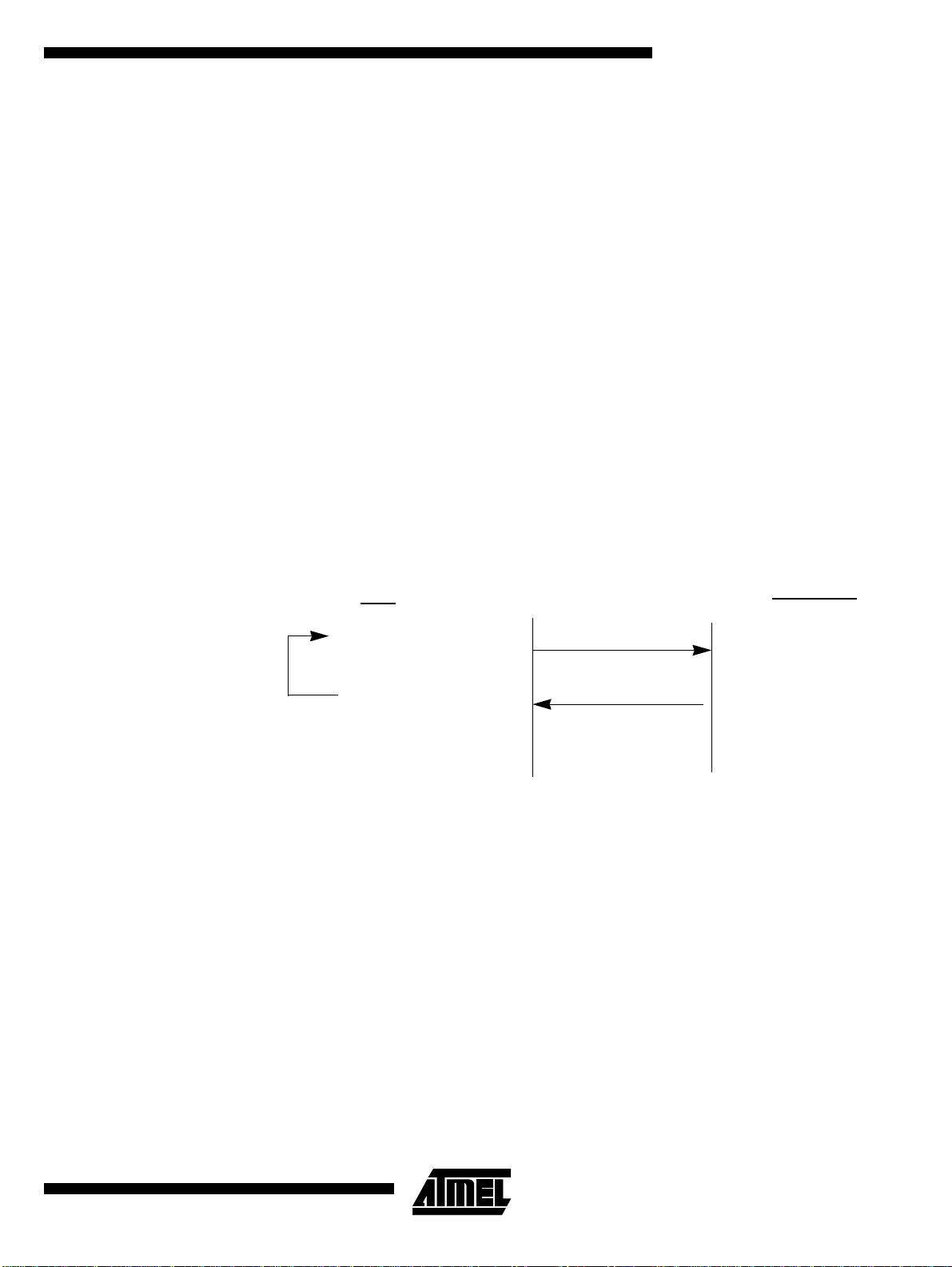
AT89C51RB2/RC2
Bootloader
r
Full Chip Erase The ISP command "Full Chip Erase " erases al l User Flash mem ory (fills with F Fh) and
sets some Bytes used by the bootloader at their default values:
• BSB = FFh
• SBV = FCh
• SSB = FFh and finally erase the Software Security Bits
The Full Chip Erase does not affect the bootloader.
Checksum Error When a checksum error is detected send ‘X’ followed with CR&LF.
Flow Description
Overview An initialization step must be performed after each Reset. After microcontroller reset,
the bootloader waits for an autobaud sequence ( see section ‘autobaud performance’).
When the comm unication is initialized the protocol depends on the record type
requested by the host.
FLIP, a so ftware u tility to im plemen t ISP p rogram ming with a PC , is avai lable from the
Atmel the web site.
Communication Initialization T he hos t initializes the comm unication by s ending a ’U’ character to help the bootloader
to compute the baudrate (autobaud).
Figure 40. Initialization
Host
Init Communication
If (not received "U")
Else
Communication Opened
"U"
"U"
Performs Autobaud
Sends Back ‘U’ Characte
4180E–8051–10/06
97
Page 98

AT89C51RB2/RC2
Autobau d Pe rf orm ances The ISP feature allows a wide range of baud rates in the user application. It is also
adaptable to a wide range of oscillator frequencies. This is accomplished by measuring
the bit-time of a sing le bit in a recei ved cha racter. This information is then used to program the baud rate in terms of timer counts based on the oscillator frequenc y. The ISP
feature requires that an initial character (an uppercase U) be sent to the
AT89C51RB2/RC2 to establish the baud rate. Table 72 shows the autobaud capability.
Table 72. Autobaud Performances
Frequency (M H z)
Baudrate (bit/s) 1.8432 2 2.4576 3 3.6864 4 5 6 7.3728 8
2400 OK OK OK OK OK OK OK OK OK OK
4800 OK - OKOKOKOKOKOKOKOK
9600 OK - OKOKOKOKOKOKOKOK
19200 OK - OK OK OK - - OK OK OK
38400 - - OK OK - OK OK OK
57600 ----OK---OK
115200 --------OK
Frequency (M H z)
Baudrate (bit/s) 10 11.0592 12 14.318 14.746 16 20 24 26.6
2400 OK OK OK OK OK OK OK OK OK
4800 OK OK OK OK OK OK OK OK OK
9600 OK OK OK OK OK OK OK OK OK
19200 OKOKOKOKOKOKOKOKOK
38400 - OK OK OK OK OK OK OK OK
57600 - OK - OKOKOKOKOKOK
115200 -OK-OKOK----
Command Data Stream
Protocol
98
All commands are sen t using the same flow. E ach frame sent by th e host is echoed by
the bootloader.
4180E–8051–10/06
Page 99
Figure 41. Command Flow
ec
AT89C51RB2/RC2
Host
Sends first character of the
Frame
":"
":"
Sends frame (made of 2 ASCII
characters per Byte)
Echo analysis
Write/Program Commands This flow is common to the following frames:
• Flash/EE PROM Programmi ng Data Frame
• EOF or Atmel Frame (only Programming Atmel Frame)
• Conf ig Byte Programming Data Frame
• Baud Rate Frame
Description
Bootloader
If (not received ":")
Else
Sends echo and start
reception
Gets frame, and sends back
for each received Byte
Figure 42. Write/Program Flow
Host
Send Write Command
OR
Wait Checksum Error
COMMAND ABORTED
OR
Wait Security Error
COMMAND ABORTED
Wait COMMAND_OK
COMMAND FINISHED
Write Command
’X’ & CR & LF
’P’ & CR & LF
’.’ & CR & LF
Bootloader
Wait Write Comman d
Checksum error
Send Checksum error
NO_SECURITY
Send Security error
Wait Programming
Send COMMAND_OK
4180E–8051–10/06
99
Page 100

AT89C51RB2/RC2
Example
Programming Data (write 55h at address 0010h in the Flash)
HOST : 01 0010 00 55 9A
BOOTLOADER : 01 0010 00 55 9A . CR LF
Programming Atmel function (write SSB to level 2)
HOST : 02 0000 03 05 01 F5
BOOTLOA DER : 02 0000 03 05 01 F5. CR LF
Writing Frame (write BSB to 55h)
HOST : 03 0000 03 06 00 55 9F
BOOTLOA DER : 03 0000 03 06 00 55 9F . CR LF
100
4180E–8051–10/06
 Loading...