


BDTIC www.bdtic.com/ATMEL
Features
• 80C52X2 Core (6 Clocks per Instruction)
– Maximum Core Frequency 48 MHz in X1 Mode, 24 MHz in X2 Mode
– Dual Data Pointer
– Full-duplex Enhanced UART (EUART)
– Three 16-bit Timer/Counters: T0, T1 and T2
– 256 Bytes of Scratchpad RAM
• 16/32-Kbyte On-chip Flash EEPROM In-System Programming through USB
– Byte and Page (128 bytes) Erase and Write
– 100k Write Cycles
• 3-KbyteFlash EEPROM for Bootloader
– Byte and Page (128 bytes) Erase and Write
– 100k Write Cycles
• 1-Kbyte EEPROM Data (
– Byte and Page (128 bytes) Erase and Write
– 100k Write Cycles
• On-chip Expanded RAM (ERAM): 1024 Bytes
• Integrated Power Monitor (POR/PFD) to Supervise Internal Power Supply
• USB 1.1 and 2.0 Full Speed Compliant Module with Interrupt on Transfer Completion
– Endpoint 0 for Control Transfers: 32-byte FIFO
– 6 Programmable Endpoints with In or Out Directions and with Bulk, Interrupt or
Isochronous Transfers
• Endpoint 1, 2, 3: 32-byte FIFO
• Endpoint 4, 5: 2 x 64-byte FIFO with Double Buffering (Ping-pong Mode)
• Endpoint 6: 2 x 512-byte FIFO with Double Buffering (Ping-pong Mode)
– Suspend/Resume Interrupts
– Power-on Reset and USB Bus Reset
– 48 MHz DPLL for Full-speed Bus Operation
– USB Bus Disconnection on Microcontroller Request
• 5 Channels Programmable Counter Array (PCA) with 16-bit Counter, High-speed
Output, Compare/Capture, PWM and Watchdog Timer Capabilities
• Programmable Hardware Watchdog Timer (One-time Enabled with Reset-out): 50 ms to
6s at 4 MHz
• Keyboard Interrupt Interface on Port P1 (8 Bits)
• TWI (Two Wire Interface) 400Kbit/s
• SPI Interface (Master/Slave Mode)
• 34 I/O Pins
• 4 Direct-drive LED Outputs with Programmable Current Sources: 2-6-10 mA Typical
• 4-level Priority Interrupt System (11 sources)
• Idle and Power-down Modes
• 0 to 32 MHz On-chip Oscillator with Analog PLL for 48 MHz Synthesis
• Industrial Temperature Range
• Low Voltage Range Supply: 2.7V to 3.6V (3.0V to 3.6V required for USB)
• Packages: SO28, PLCC52, VQFP64
8-bit Flash
Microcontroller
with Full Speed
USB Device
AT89C5131A-L
Rev. 4338F–USB–08/07

AT89C5131A-L
Description
AT89C5131A-L is a high-performance Flash version of the 80C51 single-chip 8-bit
microcontrollers with full speed USB functions.
AT89C5131A-L features a full-speed USB module compatible with the USB specifications Version 1.1 and 2.0. This module integrates the USB transceivers with a 3.3V
voltage regulator and the Serial Interface Engine (SIE) with Digital Phase Locked Loop
and 48 MHz clock recovery. USB Event detection logic (Reset and Suspend/Resume)
and FIFO buffers supporting the mandatory control Endpoint (EP0) and up to 6 versatile
Endpoints (EP1/EP2/EP3/EP4/EP5/EP6) with minimum software overhead are also part
of the USB module.
AT89C5131A-L retains the features of the Atmel 80C52 with extended Flash capacity
(3 2 -Kbyt e), 256 b ytes of int ernal R AM, a 4-l evel int errup t syste m, two 16 -bit
timer/counters (T0/ T1), a full duplex enhanced U ART (EUART) and an on-chip
oscillator.
In addition, AT89C5131A-L has an on-chip expanded RAM of 1024 bytes (ERAM), a
dual- data pointer, a 16-bit up/down Timer (T2), a Programmable Counter Array (PCA),
up to 4 programmable LED current sources, a programmable hardware watchdog and a
power-on reset.
AT89C5131A-L has two software-selectable modes of reduced activity for further reduction in power consumption. In the idle mode the CPU is frozen while the timers, the
serial ports and the interrupt system are still operating. In the power-down mode the
RAM is saved, the peripheral clock is frozen, but the device has full wake-up capability
through USB events or external interrupts.
2
4338F–USB–08/07
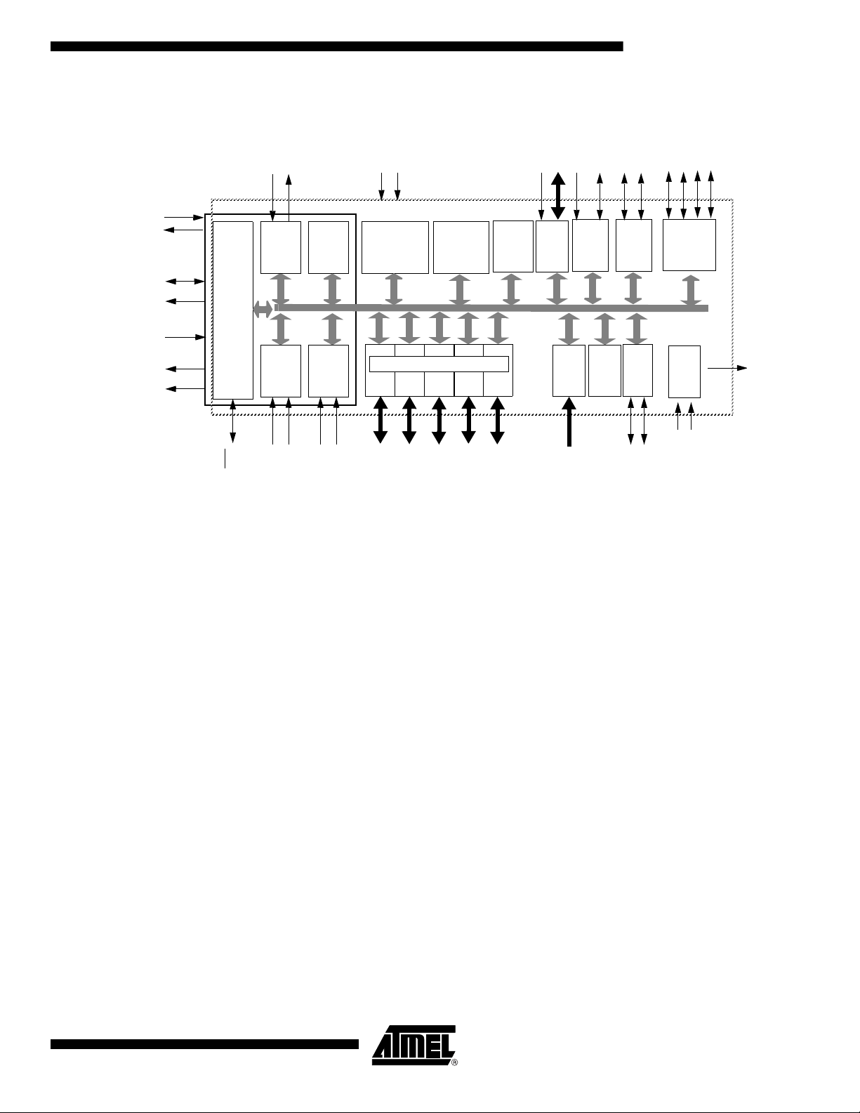
Block Diagram
Timer 0
INT
RAM
256x8
T0
T1
RxD
TxD
WR
RD
EA
PSEN
ALE
XTAL2
XTAL1
EUART
CPU
Timer 1
INT1
Ctrl
INT0
(2)
(2)
C51
CORE
(2) (2) (2) (2)
Port 0P0Port 1
Port 2
Port 3
Parallel I/O Ports & Ext. Bus
P1
P2
P3
ERAM
1Kx8
PCA
RST
Watch
Dog
CEX
ECI
VSS
VDD
(2)(2)
(1)(1)
Timer2
T2EX
T2
(1)
(1)
Port 4
P4
32Kx8 Flash
+
BRG
USB
D -
D +
VREF
Regu-
Key
Board
KIN
lator
AVSS
EEPROM
4Kx8
SPI
MISO
MOSI
SCK
(1) (1) (1)
SS
(1)
AVDD
TWI
SCL
SDA
AT89C5131A-L
Notes: 1. Alternate function of Port 1
2. Alternate function of Port 3
3. Alternate function of Port 4
4338F–USB–08/07
3
AT89C5131A-L
Pinout Description
21 22 26252423 292827 30 31
5 4 3 2 1 6
52 51 50 49 48
8
9
10
11
12
13
14
15
16
17
18
46
45
44
43
42
41
40
39
38
37
36
PLCC52
7
47
19
20
32 33
34
35
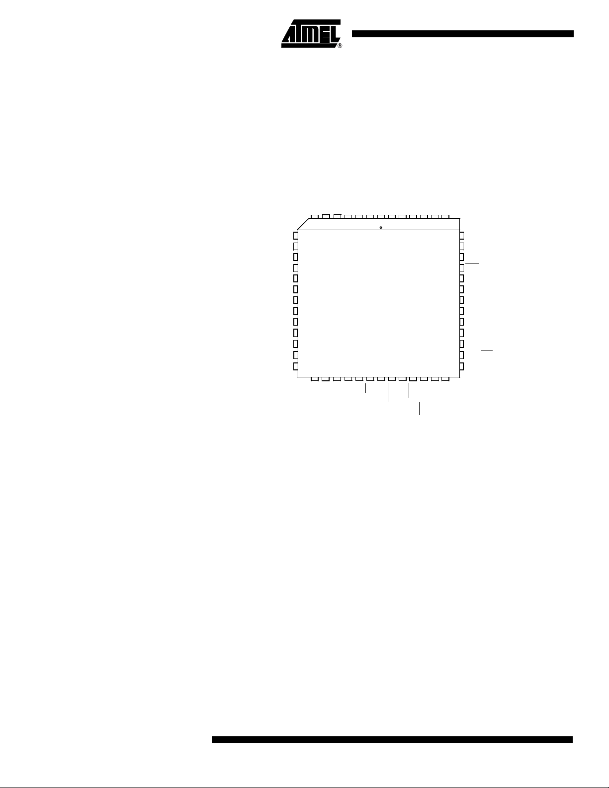
P1.1/T2EX/KIN1/SS
P1.0/T2/KIN0
P0.6/AD6
ALE
P0.7/AD7
EA
PSEN
P1.7/CEX4/KIN7/MOSI
P1.3/CEX0/KIN3
P1.5/CEX2/KIN5/MISO
P1.6/CEX3/KIN6/SCK
PLLF
P3.0/RxD
AVSS
P2.6/A14
XTAL1
P2.5/A13
P0.3/AD3
P0.5/AD5
P0.4/AD4
VREF
P0.2/AD2
P0.0/AD0
P0.1/AD1
AVDD
NC
P3.2/INT0
P3.6/WR/LED2
XTAL2
RST
P3.1/TxD
P3.3/INT1/LED0
P3.7/RD/LED3
D-
P2.0/A8
P2.1/A9
P2.2/A10
P2.3/A11
VSS
P2.4/A12
P4.1/SDA
D+
P4.0/SCL
P1.2/ECI/KIN2
P1.4/CEX1/KIN4
P3.4/T0
P3.5/T1/LED1
NC
NC
VDD
NC
P2.7/A15
Pinout
Figure 1. AT89C5131A-L 52-pin PLCC Pinout
4
4338F–USB–08/07
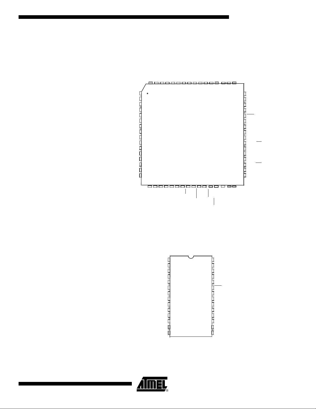
Figure 2. AT89C5131A-L 64-pin VQFP Pinout
17 18 22212019 252423 26 27
62 61 60 59 58 63
57 56 55 54 53
1
2
3
4
5
6
7
8
9
10
11
48
47
46
45
44
43
42
41
40
39
38
VQFP64
64
52
12
13
28
29
36
37
51 50
49
35
33
34
14
15
16
30
31 32
P1.1/T2EX/KIN1/SS
ALE
EA
PSEN
P1.7/CEX4/KIN7/MOSI
P1.3/CEX0/KIN3
P1.5/CEX2/KIN5/MISO
P1.6/CEX3/KIN6/SCK
P2.7/A15
P2.6/A14
P4.1/SDA
P1.2/ECI/KIN2
P1.4/CEX1/KIN4
P1.0/T2/KIN0
PLLF
NC
XTAL2
RST
P3.7/RD/LED3
P2.0/A8
P2.1/A9
P2.2/A10
P2.3/A11
P2.4/A12
NC
NC
P3.0/RxD
NC
VREF
P0.0/AD0
AVSS
P3.2/INT0
P3.6/WR/LED2
P3.1/TxD
P3.3/INT1/LED0
VSS
P3.4/T0
P3.5/T1/LED1
NC
P0.6/AD6
P0.7/AD7
P2.5/A13
P0.3/AD3
P0.5/AD5
P0.4/AD4
P0.2/AD2
P0.1/AD1
D-
D+
P4.0/SCL
XTAL1
AVDD
NC
NC
NC
NC
NC
NC
NC
NC
NC
NC
NC
VDD
P1.1/T2EX/KIN1/SS
PLLF
P3.0/RxD
P1.0/T2/KIN0
AVSS
VDD
XTAL1
XTAL2
P3.2/INT0
P3.5/T1/LED1
P3.6/WR/LED2
P3.7/RD/LED3
D-
P1.4/CEX1/KIN4
VSS
D+
P1.2/ECI/KIN2
P1.3/CEX0/KIN3
P1.5/CEX2/KIN5/MISO
RST
P1.6/CEX3/KIN6/SCK
P1.7/CEX4/KIN7/MOSI
P4.0/SCL
VREF P3.1/TxD
P3.4/T0
1
2
3
4
5
6
7
8
9
10
11
12
28
27
26
25
24
23
22
21
20
19
18
17
SO28
13
14
16
15
P4.1/SDA
P3.3/INT1/LED0
AT89C5131A-L
4338F–USB–08/07
Figure 3. AT89C5131A-L 28-pin SO Pinout
5

AT89C5131A-L
Signals
All the AT89C5131A-L signals are detailed by functionality on Table 1 through Table 12.
Table 1. Keypad Interface Signal Description
Signal
Name Type Description
KIN[7:0) I
Keypad Input Lines
Holding one of these pins high or low for 24 oscillator periods triggers a
keypad interrupt if enabled. Held line is reported in the KBCON register.
Table 2. Programmable Counter Array Signal Description
Signal
Name Type Description
ECI I External Clock Input P1.2
Capture External Input
CEX[4:0] I/O
Compare External Output
Table 3. Serial I/O Signal Description
Signal
Name Type Description
RxD I
Serial Input
The serial input for Extended UART.
Alternate
Function
P1[7:0]
Alternate
Function
P1.3
P1.4
P1.5
P1.6
P1.7
Alternate
Function
P3.0
TxD O
Serial Output
The serial output for Extended UART.
Table 4. Timer 0, Timer 1 and Timer 2 Signal Description
Signal
Name Type Description
Timer 0 Gate Input
INT0 serves as external run control for timer 0, when selected by GATE0
bit in TCON register.
INT0 I
INT1 I
External Interrupt 0
INT0 input set IE0 in the TCON register. If bit IT0 in this register is set, bits
IE0 are set by a falling edge on INT0. If bit IT0 is cleared, bits IE0 is set by
a low level on INT0.
Timer 1 Gate Input
INT1 serves as external run control for Timer 1, when selected by GATE1
bit in TCON register.
External Interrupt 1
INT1 input set IE1 in the TCON register. If bit IT1 in this register is set, bits
IE1 are set by a falling edge on INT1. If bit IT1 is cleared, bits IE1 is set by
a low level on INT1.
P3.1
Alternate
Function
P3.2
P3.3
6
4338F–USB–08/07
AT89C5131A-L
Table 4. Timer 0, Timer 1 and Timer 2 Signal Description (Continued)
Signal
Name Type Description
Alternate
Function
T0 I
T1 I
T2
T2EX I Timer/Counter 2 Reload/Capture/Direction Control Input P1.1
Timer Counter 0 External Clock Input
When Timer 0 operates as a counter, a falling edge on the T0 pin
increments the count.
Timer/Counter 1 External Clock Input
When Timer 1 operates as a counter, a falling edge on the T1 pin
increments the count.
IOTimer/Counter 2 External Clock Input
Timer/Counter 2 Clock Output
Table 5. LED Signal Description
Signal
Name Type Description
Direct Drive LED Output
LED[3:0] O
These pins can be directly connected to the Cathode of standard LEDs
without external current limiting resistors. The typical current of each
output can be programmed by software to 2, 6 or 10 mA. Several outputs
can be connected together to get higher drive capabilities.
Table 6. TWI Signal Description
Signal
Name Type Description
P3.4
P3.5
P1.0
Alternate
Function
P3.3
P3.5
P3.6
P3.7
Alternate
Function
SCL I/O
SDA I/O
SCL: TWI Serial Clock
SCL output the serial clock to slave peripherals.
SCL input the serial clock from master.
SDA: TWI Serial Data
SCL is the bidirectional TWI data line.
Table 7. SPI Signal Description
Signal
Name Type Description
SS I/O SS: SPI Slave Select P1.1
MISO: SPI Master Input Slave Output line
MISO I/O
SCK I/O
MOSI
When SPI is in master mode, MISO receives data from the slave
peripheral. When SPI is in slave mode, MISO outputs data to the master
controller.
SCK: SPI Serial Clock
SCK outputs clock to the slave peripheral or receive clock from the master
MOSI: SPI Master Output Slave Input line
I/O
When SPI is in master mode, MOSI outputs data to the slave peripheral.
When SPI is in slave mode, MOSI receives data from the master controller
P4.0
P4.1
Alternate
Function
P1.5
P1.6
P1.7
4338F–USB–08/07
7

AT89C5131A-L
Table 8. Ports Signal Description
Signal
Name Type Description Alternate Function
Port 0
P0 is an 8-bit open-drain bidirectional I/O port. Port 0
P0[7:0] I/O
P1[7:0] I/O
pins that have 1s written to them float and can be used
as high impedance inputs. To avoid any parasitic current
consumption, Floating P0 inputs must be pulled to V
VSS.
Port 1
P1 is an 8-bit bidirectional I/O port with internal pull-ups.
DD
or
AD[7:0]
KIN[7:0]
T2
T2EX
ECI
CEX[4:0]
P2[7:0] I/O
P3[7:0] I/O
P4[1:0] I/O
Port 2
P2 is an 8-bit bidirectional I/O port with internal pull-ups.
Port 3
P3 is an 8-bit bidirectional I/O port with internal pull-ups.
Port 4
P4 is an 2-bit open port.
Table 9. Clock Signal Description
Signal
Name Type Description
XTAL1 I
XTAL2 O
Input to the on-chip inverting oscillator amplifier
To use the internal oscillator, a crystal/resonator circuit is connected to this
pin. If an external oscillator is used, its output is connected to this pin.
Output of the on-chip inverting oscillator amplifier
To use the internal oscillator, a crystal/resonator circuit is connected to this
pin. If an external oscillator is used, leave XTAL2 unconnected.
A[15:8]
LED[3:0]
RxD
TxD
INT0
INT1
T0
T1
WR
RD
SCL
SDA
Alternate
Function
-
-
8
PLLF I
PLL Low Pass Filter input
Receives the RC network of the PLL low pass filter (See Figure 4 on page
11 ).
4338F–USB–08/07
-
Table 10. USB Signal Description
AT89C5131A-L
Signal
Name Type Description
D+ I/O
D- I/O
VREF O
USB Data + signal
Set to high level under reset.
USB Data - signal
Set to low level under reset.
USB Reference Voltage
Connect this pin to D+ using a 1.5 kΩ resistor to use the Detach function.
Table 11. System Signal Description
Signal
Name Type Description
AD[7:0] I/O
A[15:8] I/O
RD I/O
WR I/O
Multiplexed Address/Data LSB for external access
Data LSB for Slave port access (used for 8-bit and 16-bit modes)
Address Bus MSB for external access
Data MSB for Slave port access (used for 16-bit mode only)
Read Signal
Read signal asserted during external data memory read operation.
Control input for slave port read access cycles.
Write Signal
Write signal asserted during external data memory write operation.
Control input for slave write access cycles.
Alternate
Function
-
-
-
Alternate
Function
P0[7:0]
P2[7:0]
P3.7
P3.6
RST I/O
ALE O
PSEN O
EA I
Reset
Holding this pin low for 64 oscillator periods while the oscillator is running
resets the device. The Port pins are driven to their reset conditions when a
voltage lower than VIL is applied, whether or not the oscillator is running.
This pin has an internal pull-up resistor which allows the device to be reset
by connecting a capacitor between this pin and VSS.
Asserting RST when the chip is in Idle mode or Power-down mode returns
the chip to normal operation.
This pin is set to 0 for at least 12 oscillator periods when an internal reset
occurs (hardware watchdog or Power monitor).
Address Latch Enable Output
The falling edge of ALE strobes the address into external latch. This signal
is active only when reading or writing external memory using MOVX
instructions.
Program Strobe Enable / Hardware conditions Input for ISP
Used as input under reset to detect external hardware conditions of ISP
mode
External Access Enable
This pin must be held low to force the device to fetch code from external
program memory starting at address 0000h. It is latched during reset and
cannot be dynamically changed during operation.
-
-
-
-
4338F–USB–08/07
9

AT89C5131A-L
Table 12. Power Signal Description
Signal
Name Type Description
Alternate
Function
AVSS GND
AVDD PWR
VSS GND
VDD PWR
VREF O
Alternate Ground
AVSS is used to supply the on-chip PLL and the USB PAD.
Alternate Supply Voltage
AVDD is used to supply the on-chip PLL and the USB PAD.
Digital Ground
VSS is used to supply the buffer ring and the digital core.
Digital Supply Voltage
VDD is used to supply the buffer ring on all versions of the device.
It is also used to power the on-chip voltage regulator of the Standard
versions or the digital core of the Low Power versions.
USB pull-up Controlled Output
VREF is used to control the USB D+ 1.5 kΩ pull up.
The Vref output is in high impedance when the bit DETACH is set in the
USBCON register.
-
-
-
-
-
10
4338F–USB–08/07
Typical Application
VSS
XTAL1
XTAL2
Q
22pF
22pF
VSS
PLLF
100R
10nF
2.2nF
VSS
VSS
AVSS
VSS
D-
D+
27R
27R
VRef
1.5K
USB
D+
D-
VBUS
GND
VSS
VDD
AVDD
VDD
4.7µF
VSS
100nF
VSS
100nF
VSS
AT89C5131A-L
Recommended External components
All the external components described in the figure below must be implemented as
close as possible from the microcontroller package.
The following figure represents the typical wiring schematic.
Figure 4. Typical Application
AT89C5131A-L
4338F–USB–08/07
11
AT89C5131A-L
PCB Recommandations
D+
VRef
D-
USB Connector
Wires must be routed in Parallel and
Components must be
If possible, isolate D+ and D- signals from other signals
with ground wires
must be as short as possible
close to the
microcontroller
PLLFAVss
Components must be
Isolate filter components
with a ground wire
microcontroller
close to the
C2
C1
R
Figure 5. USB Pads
Figure 6. USB PLL
12
4338F–USB–08/07
Clock Controller
X1
X2
PD
PCON.1
IDL
PCON.0
Peripheral
CPU Core
0
1
X2
CKCON.0
÷
2
Clock
Clock
EXT48
PLLCON.2
0
1
PLL
USB
Clock
AT89C5131A-L
Introduction
Figure 7. Oscillator Block Diagram
The AT89C5131A-L clock controller is based on an on-chip oscillator feeding an on-chip
Phase Lock Loop (PLL). All the internal clocks to the peripherals and CPU core are generated by this controller.
The AT89C5131A-L X1 and X2 pins are the input and the output of a single-stage onchip inverter (see Figure 7) that can be configured with off-chip components as a Pierce
oscillator (see Figure 8). Value of capacitors and crystal characteristics are detailed in
the section “DC Characteristics”.
The X1 pin can also be used as input for an external 48 MHz clock.
The clock controller outputs three different clocks as shown in Figure 7:
• a clock for the CPU core
• a clock for the peripherals which is used to generate the Timers, PCA, WD, and Port
sampling clocks
• a clock for the USB controller
These clocks are enabled or disabled depending on the power reduction mode as
detailed in Section “Power Management”, page 152.
Oscillator
4338F–USB–08/07
Two clock sources are available for CPU:
• Crystal oscillator on X1 and X2 pins: Up to 32 MHz
• External 48 MHz clock on X1 pin
In order to optimize the power consumption, the oscillator inverter is inactive when the
PLL output is not selected for the USB device.
13
AT89C5131A-L
Figure 8. Crystal Connection
VSS
X1
X2
Q
C1
C2
PLLEN
PLLCON.1
N3:0
N divider
R divider
VCO USB Clock
US Bclk
OSCclk R 1+( )×
N 1+
-----------------------------------------------=
OSC
CLOCK
PFLD
PLOCK
PLLCON.0
PLLF
CHP
Vref
Up
Down
R3:0
USB
CLOCK
USB Clock Symbol
VSS
PLLF
R
C1
C2
VSS
PLL
PLL Description The AT89C5131A-L PLL is used to generate internal high frequency clock (the USB
Clock) synchronized with an external low-frequency (the Peripheral Clock). The PLL
clock is used to generate the USB interface clock. Figure 9 shows the internal structure
of the PLL.
The PFLD block is the Phase Frequency Comparator and Lock Detector. This block
makes the comparison between the reference clock coming from the N divider and the
reverse clock coming from the R divider and generates some pulses on the Up or Down
signal depending on the edge position of the reverse clock. The PLLEN bit in PLLCON
register is used to enable the clock generation. When the PLL is locked, the bit PLOCK
in PLLCON register (see Figure 9) is set.
The CHP block is the Charge Pump that generates the voltage reference for the VCO by
injecting or extracting charges from the external filter connected on PLLF pin (see
Figure 10 ) . Value o f the fil ter c o m p onents a r e d etailed i n t h e Section “ D C
Characteristics”.
Figure 9. PLL Block Diagram and Symbol
The VCO block is the Voltage Controlled Oscillator controlled by the voltage V
duced by the charge pump. It generates a square wave signal: the PLL clock.
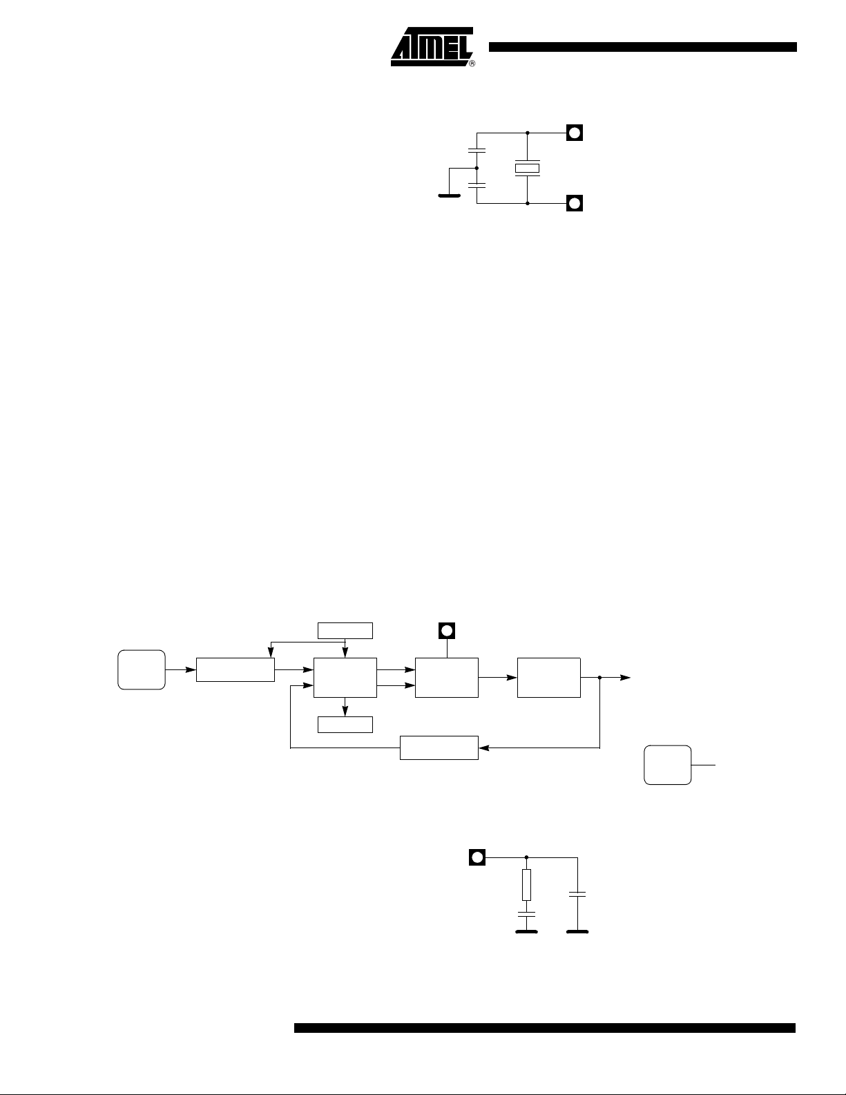
Figure 10. PLL Filter Connection
The typical values are: R = 100 Ω, C1 = 10 nf, C2 = 2.2 nF.
REF
pro-
14
4338F–USB–08/07
AT89C5131A-L
PLL
Programming
Configure Dividers
N3:0 = xxxxb
R3:0 = xxxxb
Enable PLL
PLLEN = 1
PLL Locked?
LOCK = 1?
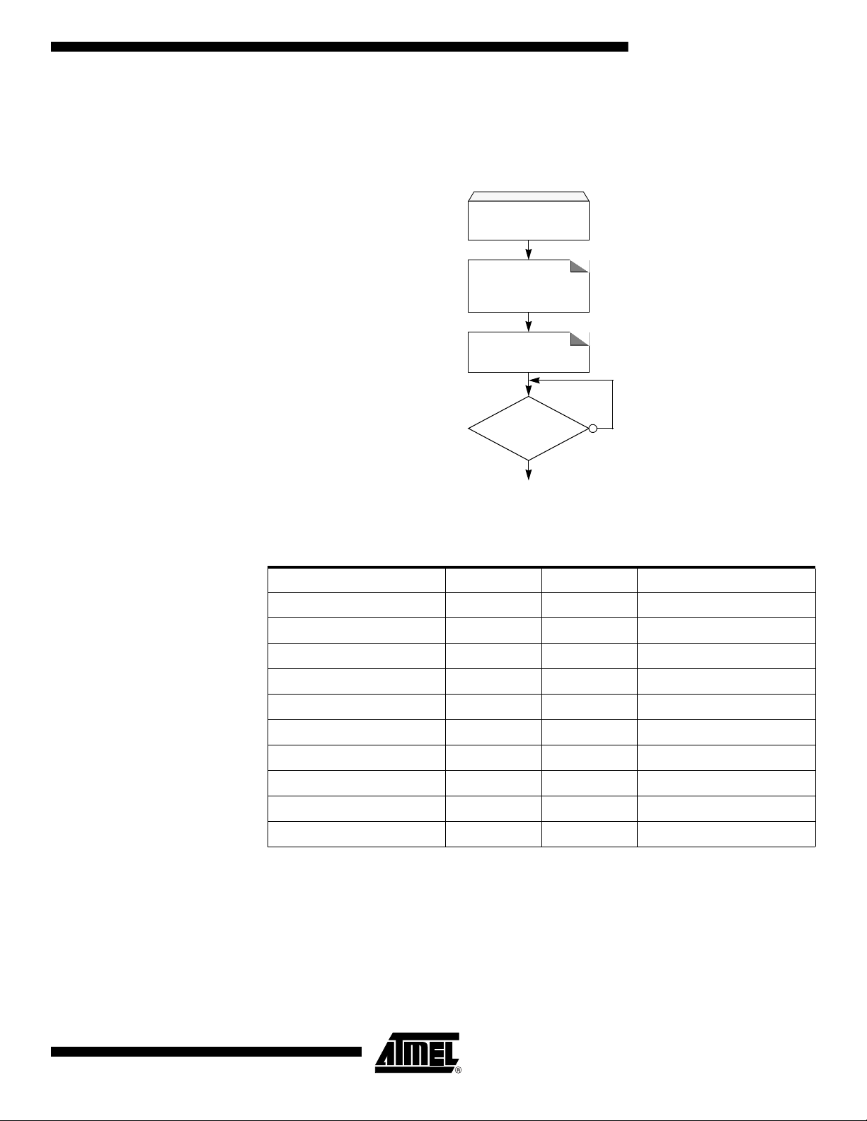
PLL Programming The PLL is programmed using the flow shown in Figure 11. As soon as clock generation
is enabled user must wait until the lock indicator is set to ensure the clock output is
stable.
Figure 11. PLL Programming Flow
Divider Values To generate a 48 MHz clock using the PLL, the divider values have to be configured fol-
lowing the oscillator frequency. The typical divider values are shown in Table 13.
Table 13. Typical Divider Values
Oscillator Frequency R+1 N+1 PLLDIV
3 MHz 16 1 F0h
6 MHz 8 1 70h
8 MHz 6 1 50h
12 MHz 4 1 30h
16 MHz 3 1 20h
18 MHz 8 3 72h
20 MHz 12 5 B4h
24 MHz 2 1 10h
32 MHz 3 2 21h
40 MHz 12 10 B9h
4338F–USB–08/07
15

AT89C5131A-L
Registers
Table 14. CKCON0 (S:8Fh)
Clock Control Register 0
7 6 5 4 3 2 1 0
TWIX2 WDX2 PCAX2 SIX2 T2X2 T1X2 T0X2 X2
Bit Number
7 TWIX2
6 WDX2
5 PCAX2
4 SIX2
3 T2X2
Bit
Mnemonic Description
TWI Clock
This control bit is validated when the CPU clock X2 is set. When X2 is low,
this bit has no effect.
Clear to select 6 clock periods per peripheral clock cycle.
Set to select 12 clock periods per peripheral clock cycle.
Watchdog Clock
This control bit is validated when the CPU clock X2 is set. When X2 is low,
this bit has no effect.
Clear to select 6 clock periods per peripheral clock cycle.
Set to select 12 clock periods per peripheral clock cycle.
Programmable Counter Array Clock
This control bit is validated when the CPU clock X2 is set. When X2 is low,
this bit has no effect.
Clear to select 6 clock periods per peripheral clock cycle.
Set to select 12 clock periods per peripheral clock cycle.
Enhanced UART Clock (Mode 0 and 2)
This control bit is validated when the CPU clock X2 is set. When X2 is low,
this bit has no effect.
Clear to select 6 clock periods per peripheral clock cycle.
Set to select 12 clock periods per peripheral clock cycle.
Timer2 Clock
This control bit is validated when the CPU clock X2 is set. When X2 is low,
this bit has no effect.
Clear to select 6 clock periods per peripheral clock cycle.
Set to select 12 clock periods per peripheral clock cycle.
16
Timer1 Clock
2 T1X2
1 T0X2
0 X2
This control bit is validated when the CPU clock X2 is set. When X2 is low,
this bit has no effect.
Clear to select 6 clock periods per peripheral clock cycle.
Set to select 12 clock periods per peripheral clock cycle.
Timer0 Clock
This control bit is validated when the CPU clock X2 is set. When X2 is low,
this bit has no effect.
Clear to select 6 clock periods per peripheral clock cycle.
Set to select 12 clock periods per peripheral clock cycle.
System Clock Control bit
Clear to select 12 clock periods per machine cycle (STD mode, F
F
OSC
Set to select 6 clock periods per machine cycle (X2 mode, F
Reset Value = 0000 0000b
= F
CPU
/
2).
CPU = FPER = FOSC
PER =
).
4338F–USB–08/07
AT89C5131A-L
Table 15. CKCON1 (S:AFh)
Clock Control Register 1
7 6 5 4 3 2 1 0
- - - - - - - SPIX2
Bit Number
7-1 -
0 SPIX2
Bit
Mnemonic Description
Reserved
The value read from this bit is always 0. Do not set this bit.
SPI Clock
This control bit is validated when the CPU clock X2 is set. When X2 is low,
this bit has no effect.
Clear to select 6 clock periods per peripheral clock cycle.
Set to select 12 clock periods per peripheral clock cycle.
Reset Value = 0000 0000b
Table 16. PLLCON (S:A3h)
PLL Control Register
7 6 5 4 3 2 1 0
- - - - - EXT48 PLLEN PLOCK
Bit Number
7-3 -
2 EXT48
Bit
Mnemonic Description
Reserved
The value read from this bit is always 0. Do not set this bit.
External 48 MHz Enable Bit
Set this bit to bypass the PLL and disable the crystal oscillator.
Clear this bit to select the PLL output as USB clock and to enable the crystal
oscillator.
4338F–USB–08/07
PLL Enable Bit
1 PLLEN
0 PLOCK
Set to enable the PLL.
Clear to disable the PLL.
PLL Lock Indicator
Set by hardware when PLL is locked.
Clear by hardware when PLL is unlocked.
Reset Value = 0000 0000b
Table 17. PLLDIV (S:A4h)
PLL Divider Register
7 6 5 4 3 2 1 0
R3 R2 R1 R0 N3 N2 N1 N0
Bit Number
7-4 R3:0 PLL R Divider Bits
3-0 N3:0 PLL N Divider Bits
Bit
Mnemonic Description
Reset Value = 0000 0000
17

AT89C5131A-L
SFR Mapping
The Special Function Registers (SFRs) of the AT89C5131A-L fall into the following
categories:
• C51 core registers: ACC, B, DPH, DPL, PSW, SP
• I/O port registers: P0, P1, P2, P3, P4
• Timer registers: T2CON, T2MOD, TCON, TH0, TH1, TH2, TMOD, TL0, TL1, TL2,
RCAP2L, RCAP2H
• Serial I/O port registers: SADDR, SADEN, SBUF, SCON
• PCA (Programmable Counter Array) registers: CCON, CMOD, CCAPMx, CL, CH,
CCAPxH, CCAPxL (x: 0 to 4)
• Power and clock control registers: PCON
• Hardware Watchdog Timer registers: WDTRST, WDTPRG
• Interrupt system registers: IEN0, IPL0, IPH0, IEN1, IPL1, IPH1
• Keyboard Interface registers: KBE, KBF, KBLS
• LED register: LEDCON
• Two Wire Interface (TWI) registers: SSCON, SSCS, SSDAT, SSADR
• Serial Port Interface (SPI) registers: SPCON, SPSTA, SPDAT
• USB registers: Uxxx (17 registers)
• PLL registers: PLLCON, PLLDIV
• BRG (Baud Rate Generator) registers: BRL, BDRCON
• Flash register: FCON (FCON access is reserved for the Flash API and ISP
software)
• EEPROM register: EECON
• Others: AUXR, AUXR1, CKCON0, CKCON1
18
4338F–USB–08/07

Table 18. SFR Descriptions
Reserved
Bit
Addressable Non-Bit Addressable
0/8 1/9 2/A 3/B 4/C 5/D 6/E 7/F
AT89C5131A-L
The table below shows all SFRs with their address and their reset value.
F8h
F0h
E8h
E0h
D8h
D0h
C8h
C0h
B8h
B0h
UEPINT
0000 0000
B
0000 0000
ACC
0000 0000
CCON
00X0 0000
PSW
0000 0000
T2CON
0000 0000
P4
XXXX 1111
IPL0
X000 000
P3
1111 1111
CH
0000 0000
LEDCON
0000 0000
CL
0000 0000
CMOD
00XX X000
FCON (1)
XXXX 0000
T2MOD
XXXX XX00
SADEN
0000 0000
IEN1
X0XX X000
CCAP0H
XXXX XXXX
CCAP0L
XXXX XXXX
UBYCTLX
0000 0000
CCAPM0
X000 0000
EECON
XXXX XX00
RCAP2L
0000 0000
UEPIEN
0000 0000
UFNUML
0000 0000
IPL1
X0XX X000
CCAP1H
XXXX XXXX
CCAP1L
XXXX XXXX
UBYCTHX
0000 0000
CCAPM1
X000 0000
RCAP2H
0000 0000
SPCON
0001 0100
UFNUMH
0000 0000
IPH1
X0XX X000
CCAP2H
XXXX XXXX
CCAP2L
XXXX XXXX
CCAPM2
X000 0000
UEPCONX
1000 0000
TL2
0000 0000
SPSTA
0000 0000
USBCON
0000 0000
CCAP3H
XXXX XXXX
CCAP3L
XXXX XXXX
CCAPM3
X000 0000
UEPRST
0000 0000
TH2
0000 0000
SPDAT
XXXX XXXX
USBINT
0000 0000
CCAP4H
XXXX XXXX
CCAP4L
XXXX XXXX
CCAPM4
X000 0000
UEPSTAX
0000 0000
USBADDR
1000 0000
USBIEN
0000 0000
UEPDATX
0000 0000
UEPNUM
0000 0000
IPH0
X000 0000
FFh
F7h
EFh
E7h
DFh
D7h
CFh
C7h
BFh
B7h
A8h
A0h
98h
90h
88h
80h
IEN0
0000 0000
P2
1111 1111
SCON
0000 0000
P1
1111 1111
TCON
0000 0000
P0
1111 1111
0/8 1/9 2/A 3/B 4/C 5/D 6/E 7/F
SADDR
0000 0000
SBUF
XXXX XXXX
TMOD
0000 0000
SP
0000 0111
AUXR1
XXXX X0X0
BRL
0000 0000
TL0
0000 0000
DPL
0000 0000
PLLCON
XXXX XX00
BDRCON
XXX0 0000
SSCON
0000 0000
TL1
0000 0000
DPH
0000 0000
0000 0000
0000 0000
1111 1000
0000 0000
Note: 1. FCON access is reserved for the Flash API and ISP software.
PLLDIV
KBLS
SSCS
TH0
KBE
0000 0000
SSDAT
1111 1111
TH1
0000 0000
WDTRST
XXXX XXXX
KBF
0000 0000
SSADR
1111 1110
AUXR
XX0X 0000
CKCON1
0000 0000
WDTPRG
XXXX X000
CKCON0
0000 0000
PCON
00X1 0000
AFh
A7h
9Fh
97h
8Fh
87h
4338F–USB–08/07
19

AT89C5131A-L
The Special Function Registers (SFRs) of the AT89C5131 fall into the following
categories:
Table 19. C51 Core SFRs
Mnemonic Add Name 7 6 5 4 3 2 1 0
ACC E0h Accumulator
B F0h B Register
PSW D0h
SP 81h
DPL 82h
DPH 83h
Program Status
Word
Stack Pointer
LSB of SPX
Data Pointer
Low byte
LSB of DPTR
Data Pointer
High byte
MSB of DPTR
Table 20. I/O Port SFRs
Mnemonic Add Name 7 6 5 4 3 2 1 0
P0 80h Port 0
P1 90h Port 1
P2 A0h Port 2
P3 B0h Port 3
P4 C0h Port 4 (2bits)
20
4338F–USB–08/07

AT89C5131A-L
Table 21. Timer SFR’s
Mnemonic Add Name 7 6 5 4 3 2 1 0
TH0 8Ch Timer/Counter 0 High byte
TL0 8Ah Timer/Counter 0 Low byte
TH1 8Dh Timer/Counter 1 High byte
TL1 8Bh Timer/Counter 1 Low byte
TH2 CDh Timer/Counter 2 High byte
TL2 CCh Timer/Counter 2 Low byte
TCON 88h
TMOD 89h
T2CON C8h Timer/Counter 2 control TF2 EXF2 RCLK TCLK EXEN2 TR2 C/T2# CP/RL2#
T2MOD C9h Timer/Counter 2 Mode T2OE DCEN
RCAP2H CBh
RCAP2L CAh
WDTRST A6h WatchDog Timer Reset
WDTPRG A7h WatchDog Timer Program S2 S1 S0
Timer/Counter 0 and 1
control
Timer/Counter 0 and 1
Modes
Timer/Counter 2
Reload/Capture High byte
Timer/Counter 2
Reload/Capture Low byte
TF1 TR1 TF0 TR0 IE1 IT1 IE0 IT0
GATE1 C/T1# M11 M01 GATE0 C/T0# M10 M00
Table 22. Serial I/O Port SFR’s
Mnemonic Add Name 7 6 5 4 3 2 1 0
SCON 98h Serial Control FE/SM0 SM1 SM2 REN TB8 RB8 TI RI
SBUF 99h Serial Data Buffer
SADEN B9h Slave Address Mask
SADDR A9h Slave Address
Table 23. Baud Rate Generator SFR’s
Mnemonic Add Name 7 6 5 4 3 2 1 0
BRL 9Ah Baud Rate Reload
BDRCON 9Bh Baud Rate Control BRR TBCK RBCK SPD SRC
4338F–USB–08/07
21

AT89C5131A-L
Table 24. PCA SFR’s
Mnemonic Add Name 7 6 5 4 3 2 1 0
CCON D8h PCA Timer/Counter Control CF CR CCF4 CCF3 CCF2 CCF1 CCF0
CMOD D9h PCA Timer/Counter Mode CIDL WDTE CPS1 CPS0 ECF
CL E9h PCA Timer/Counter Low byte
CH F9h PCA Timer/Counter High byte
CCAPM0
CCAPM1
CCAPM2
CCAPM3
CCAPM4
CCAP0H
CCAP1H
CCAP2H
CCAP3H
CCAP4H
CCAP0L
CCAP1L
CCAP2L
CCAP3L
CCAP4L
DAh
PCA Timer/Counter Mode 0
DBh
PCA Timer/Counter Mode 1
DCh
PCA Timer/Counter Mode 2
DDh
PCA Timer/Counter Mode 3
DEh
PCA Timer/Counter Mode 4
FAh
PCA Compare Capture Module 0 H
FBh
PCA Compare Capture Module 1 H
FCh
PCA Compare Capture Module 2 H
FDh
PCA Compare Capture Module 3 H
FEh
PCA Compare Capture Module 4 H
EAh
PCA Compare Capture Module 0 L
EBh
PCA Compare Capture Module 1 L
ECh
PCA Compare Capture Module 2 L
EDh
PCA Compare Capture Module 3 L
EEh
PCA Compare Capture Module 4 L
CCAP0H7
CCAP1H7
CCAP2H7
CCAP3H7
CCAP4H7
CCAP0L7
CCAP1L7
CCAP2L7
CCAP3L7
CCAP4L7
ECOM0
ECOM1
ECOM2
ECOM3
ECOM4
CCAP0H6
CCAP1H6
CCAP2H6
CCAP3H6
CCAP4H6
CCAP0L6
CCAP1L6
CCAP2L6
CCAP3L6
CCAP4L6
CAPP0
CAPP1
CAPP2
CAPP3
CAPP4
CCAP0H5
CCAP1H5
CCAP2H5
CCAP3H5
CCAP4H5
CCAP0L5
CCAP1L5
CCAP2L5
CCAP3L5
CCAP4L5
CAPN0
CAPN1
CAPN2
CAPN3
CAPN4
CCAP0H4
CCAP1H4
CCAP2H4
CCAP3H4
CCAP4H4
CCAP0L4
CCAP1L4
CCAP2L4
CCAP3L4
CCAP4L4
MAT0
MAT1
MAT2
MAT3
MAT4
CCAP0H3
CCAP1H3
CCAP2H3
CCAP3H3
CCAP4H3
CCAP0L3
CCAP1L3
CCAP2L3
CCAP3L3
CCAP4L3
TOG0
TOG1
TOG2
TOG3
TOG4
CCAP0H2
CCAP1H2
CCAP2H2
CCAP3H2
CCAP4H2
CCAP0L2
CCAP1L2
CCAP2L2
CCAP3L2
CCAP4L2
PWM0
PWM1
PWM2
PWM3
PWM4
CCAP0H1
CCAP1H1
CCAP2H1
CCAP3H1
CCAP4H1
CCAP0L1
CCAP1L1
CCAP2L1
CCAP3L1
CCAP4L1
ECCF0
ECCF1
ECCF2
ECCF3
ECCF4
CCAP0H0
CCAP1H0
CCAP2H0
CCAP3H0
CCAP4H0
CCAP0L0
CCAP1L0
CCAP2L0
CCAP3L0
CCAP4L0
Table 25. Interrupt SFR’s
Mnemonic Add Name 7 6 5 4 3 2 1 0
IEN0 A8h Interrupt Enable Control 0 EA EC ET2 ES ET1 EX1 ET0 EX0
IEN1 B1h Interrupt Enable Control 1 EUSB ESPI ETWI EKB
IPL0 B8h Interrupt Priority Control Low 0 PPCL PT2L PSL PT1L PX1L PT0L PX0L
IPH0 B7h Interrupt Priority Control High 0 PPCH PT2H PSH PT1H PX1H PT0H PX0H
IPL1 B2h Interrupt Priority Control Low 1 PUSBL PSPIL PTWIL PKBL
IPH1 B3h Interrupt Priority Control High 1 PUSBH PSPIH PTWIH PKBH
Table 26. PLL SFRs
Mnemonic Add Name 7 6 5 4 3 2 1 0
PLLCON A3h PLL Control EXT48 PLLEN PLOCK
PLLDIV A4h PLL Divider R3 R2 R1 R0 N3 N2 N1 N0
22
4338F–USB–08/07

AT89C5131A-L
Table 27. Keyboard SFRs
Mnemonic Add Name 7 6 5 4 3 2 1 0
KBF 9Eh
KBE 9Dh
KBLS 9Ch
Keyboard Flag
Register
Keyboard Input Enable
Register
Keyboard Level
Selector Register
KBF7 KBF6 KBF5 KBF4 KBF3 KBF2 KBF1 KBF0
KBE7 KBE6 KBE5 KBE4 KBE3 KBE2 KBE1 KBE0
KBLS7 KBLS6 KBLS5 KBLS4 KBLS3 KBLS2 KBLS1 KBLS0
Table 28. TWI SFRs
Mnemonic Add Name 7 6 5 4 3 2 1 0
SSCON 93h
SSCS 94h
SSDAT 95h
SSADR 96h
Synchronous Serial
Control
Synchronous Serial
Control-Status
Synchronous Serial
Data
Synchronous Serial
Address
CR2 SSIE STA STO SI AA CR1 CR0
SC4 SC3 SC2 SC1 SC0 - - -
SD7 SD6 SD5 SD4 SD3 SD2 SD1 SD0
A7 A6 A5 A4 A3 A2 A1 A0
Table 29. SPI SFRs
Mnemonic Add Name 7 6 5 4 3 2 1 0
SPCON C3h
SPSTA C4h
SPDAT C5h Serial Peripheral Data R7 R6 R5 R4 R3 R2 R1 R0
Serial Peripheral
Control
Serial Peripheral
Status-Control
SPR2 SPEN SSDIS MSTR CPOL CPHA SPR1 SPR0
SPIF WCOL SSERR MODF - - - -
Table 30. USB SFR’s
Mnemonic Add Name 7 6 5 4 3 2 1 0
USBCON BCh USB Global Control USBE SUSPCLK SDRMWUP DETACH UPRSM RMWUPE CONFG FADDEN
USBADDR C6h USB Address FEN UADD6 UADD5 UADD4 UADD3 UADD2 UADD1 UADD0
USBINT BDh USB Global Interrupt - - WUPCPU EORINT SOFINT - - SPINT
USBIEN BEh
UEPNUM C7h USB Endpoint Number - - - - EPNUM3 EPNUM2 EPNUM1 EPNUM0
UEPCONX D4h USB Endpoint X Control EPEN - - - DTGL EPDIR EPTYPE1 EPTYPE0
UEPSTAX CEh USB Endpoint X Status DIR RXOUTB1 STALLRQ TXRDY STLCRC RXSETUP RXOUTB0 TXCMP
UEPRST D5h USB Endpoint Reset - EP6RST EP5RST EP4RST EP3RST EP2RST EP1RST EP0RST
UEPINT F8h USB Endpoint Interrupt - EP6INT EP5INT EP4INT EP3INT EP2INT EP1INT EP0INT
USB Global Interrupt
Enable
- - EWUPCPU EEORINT ESOFINT - - ESPINT
4338F–USB–08/07
23

AT89C5131A-L
Table 30. USB SFR’s
Mnemonic Add Name 7 6 5 4 3 2 1 0
UEPIEN C2h
UEPDATX CFh USB Endpoint X FIFO Data FDAT7 FDAT6 FDAT5 FDAT4 FDAT3 FDAT2 FDAT1 FDAT0
UBYCTLX E2h
UBYCTHX E3h
UFNUML BAh USB Frame Number Low FNUM7 FNUM6 FNUM5 FNUM4 FNUM3 FNUM2 FNUM1 FNUM0
UFNUMH BBh USB Frame Number High - - CRCOK CRCERR - FNUM10 FNUM9 FNUM8
USB Endpoint Interrupt
Enable
USB Byte Counter Low (EP
X)
USB Byte Counter High
(EP X)
- EP6INTE EP5INTE EP4INTE EP3INTE EP2INTE EP1INTE EP0INTE
BYCT7 BYCT6 BYCT5 BYCT4 BYCT3 BYCT2 BYCT1 BYCT0
- - - - - BYCT10 BYCT9 BYCT8
Table 31. Other SFR’s
Mnemonic Add Name 7 6 5 4 3 2 1 0
PCON 87h Power Control SMOD1 SMOD0 - POF GF1 GF0 PD IDL
AUXR 8Eh Auxiliary Register 0 DPU - M0 - XRS1 XRS2 EXTRAM A0
AUXR1 A2h Auxiliary Register 1 - - ENBOOT - GF3 - - DPS
CKCON0 8Fh Clock Control 0 TWIX2 WDX2 PCAX2 SIX2 T2X2 T1X2 T0X2 X2
CKCON1 AFh Clock Control 1 - - - - - - - SPIX2
LEDCON F1h LED Control LED3 LED2 LED1 LED0
FCON D1h Flash Control FPL3 FPL2 FPL1 FPL0 FPS FMOD1 FMOD0 FBUSY
EECON D2h EEPROM Contol EEPL3 EEPL2 EEPL1 EEPL0 - - EEE EEBUSY
24
4338F–USB–08/07
AT89C5131A-L
External Data Memory
AUXR1(A2H)
DPS
DPH(83H) DPL(82H)
07
DPTR0
DPTR1
Dual Data Pointer Register
Figure 12. Use of Dual Pointer
The additional data pointer can be used to speed up code execution and reduce code
size.
The dual DPTR structure is a way by which the chip will specify the address of an external data memory location. There are two 16-bit DPTR registers that address the external
memory, and a single bit called DPS = AUXR1.0 (see Table 32) that allows the program
code to switch between them (see Figure 12).
Table 32. AUXR1 Register
AUXR1- Auxiliary Register 1(0A2h)
7 6 5 4 3 2 1 0
- - ENBOOT - GF3 0 - DPS
Bit
Number
7 -
6 -
5 ENBOOT
4 -
3 GF3 This bit is a general-purpose user flag.
2 0 Always cleared.
1 -
0 DPS
Bit
Mnemonic Description
Reserved
The value read from this bit is indeterminate. Do not set this bit.
Reserved
The value read from this bit is indeterminate. Do not set this bit.
Enable Boot Flash
Cleared to disable boot ROM.
Set to map the boot ROM between F800h - 0FFFFh.
Reserved
The value read from this bit is indeterminate. Do not set this bit.
Reserved
The value read from this bit is indeterminate. Do not set this bit.
Data Pointer Selection
Cleared to select DPTR0.
Set to select DPTR1.
Reset Value = XX[BLJB]X X0X0b
Not bit addressable
4338F–USB–08/07
a. Bit 2 stuck at 0; this allows to use INC AUXR1 to toggle DPS without changing GF3.
25

AT89C5131A-L
ASSEMBLY LANGUAGE
; Block move using dual data pointers
; Modifies DPTR0, DPTR1, A and PSW
; note: DPS exits opposite of entry state
; unless an extra INC AUXR1 is added
;
00A2 AUXR1 EQU 0A2H
;
0000 909000MOV DPTR,#SOURCE ; address of SOURCE
0003 05A2 INC AUXR1 ; switch data pointers
0005 90A000 MOV DPTR,#DEST ; address of DEST
0008 LOOP:
0008 05A2 INC AUXR1 ; switch data pointers
000A E0 MOVX A,@DPTR ; get a byte from SOURCE
000B A3 INC DPTR ; increment SOURCE address
000C 05A2 INC AUXR1 ; switch data pointers
000E F0 MOVX @DPTR,A ; write the byte to DEST
000F A3 INC DPTR ; increment DEST address
0010 70F6JNZ LOOP ; check for 0 terminator
0012 05A2 INC AUXR1 ; (optional) restore DPS
INC is a short (2 bytes) and fast (12 clocks) way to manipulate the DPS bit in the AUXR1
SFR. However, note that the INC instruction does not directly force the DPS bit to a particular state, but simply toggles it. In simple routines, such as the block move example,
only the fact that DPS is toggled in the proper sequence matters, not its actual value. In
other words, the block move routine works the same whether DPS is '0' or '1' on entry.
Observe that without the last instruction (INC AUXR1), the routine will exit with DPS in
the opposite state.
26
4338F–USB–08/07
AT89C5131A-L
0000h
32 Kbytes
7FFFh
Flash
32 Kbytes
External Code
FFFFh
AT89C5131A-L
8000h
Flash
EPROM
AT89C5131
P2
P0
AD7:0
A15:8
A7:0
A15:8
D7:0
A7:0
ALE
Latch
OEPSEN
Program/Code Memory
The AT89C5131A-L implement 32 Kbytes of on-chip program/code memory. Figure 13
shows the split of internal and external program/code memory spaces depending on the
product.
The Flash memory increases EPROM and ROM functionality by in-circuit electrical erasure and programming. Thanks to the internal charge pump, the high voltage needed for
programming or erasing Flash cells is generated on-chip using the standard VDD voltage. Thus, the Flash Memory can be programmed using only one voltage and allows Inapplication Software Programming commonly known as IAP. Hardware programming
mode is also available using specific programming tool.
Figure 13. Program/Code Memory Organization
Note: If the program executes exclusively from on-chip code memory (not from external mem-
ory), beware of executing code from the upper byte of on-chip memory (7FFFh) and
thereby disrupting I/O Ports 0 and 2 due to external prefetch. Fetching code constant
from this location does not affect Ports 0 and 2.
External Code Memory Access
Memory Interface The external memory interface comprises the external bus (Port 0 and Port 2) as well as
the bus control signals (PSEN, and ALE).
Figure 14 shows the structure of the external address bus. P0 carries address A7:0
while P2 carries address A15:8. Data D7:0 is multiplexed with A7:0 on P0. Table 33
describes the external memory interface signals.
Figure 14. External Code Memory Interface Structure
4338F–USB–08/07
27
AT89C5131A-L
Table 33. External Data Memory Interface Signals
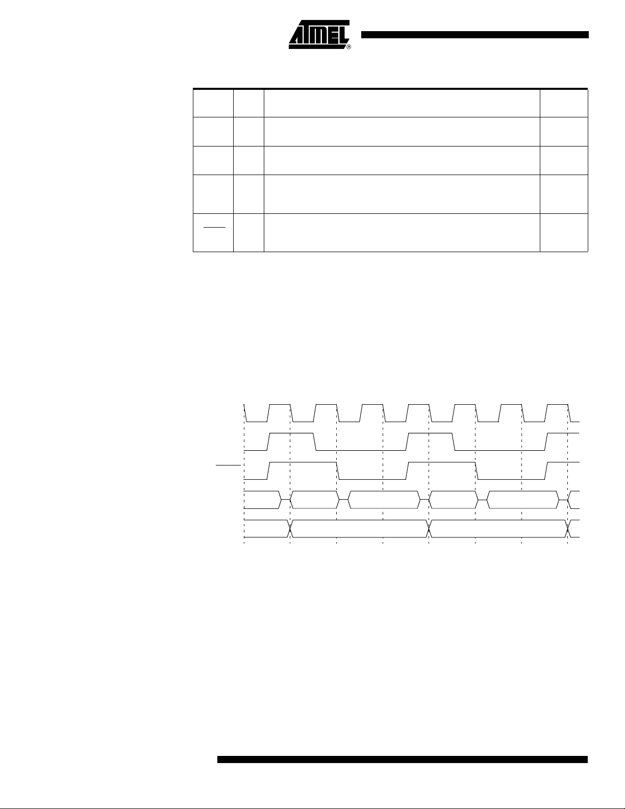
ALE
P0
P2
PSEN
PCL
PCHPCH
PCLD7:0 D7:0
PCH
D7:0
CPU Clock
Signal
Name Type Description
A15:8 O
AD7:0 I/O
ALE O
PSEN O
Address Lines
Upper address lines for the external bus.
Address/Data Lines
Multiplexed lower address lines and data for the external memory.
Address Latch Enable
ALE signals indicates that valid address information are available on lines
AD7:0.
Program Store Enable Output
This signal is active low during external code fetch or external code read
(MOVC instruction).
Alternate
Function
P2.7:0
P0.7:0
-
-
External Bus Cycles This section describes the bus cycles the AT89C5131A-L executes to fetch code (see
Figure 15) in the external program/code memory.
External memory cycle takes 6 CPU clock periods. This is equivalent to 12 oscillator
clock periods in standard mode or 6 oscillator clock periods in X2 mode. For further
information on X2 mode (see the clock Section).
For simplicity, the accompanying figure depicts the bus cycle waveforms in idealized
form and do not provide precise timing information.
Figure 15. External Code Fetch Waveforms
Flash Memory Architecture
28
AT89C5131A-L features two on-chip Flash memories:
• Flash memory FM0:
containing 32 Kbytes of program memory (user space) organized into 128-byte
pages,
• Flash memory FM1:
3 Kbytes for bootloader and Application Programming Interfaces (API).
The FM0 supports both parallel programming and Serial In-System Programming (ISP)
whereas FM1 supports only parallel programming by programmers. The ISP mode is
detailed in the “In-System Programming” section.
All Read/Write access operations on Flash memory by user application are managed by
a set of API described in the “In-System Programming” section.
4338F–USB–08/07

Figure 16. Flash Memory Architecture
7FFFh
32 Kbytes
Flash Memory
FM0
0000h
Hardware Security (1 Byte)
Column Latches (128 Bytes)
User Space
Extra Row (128 Bytes)
3 Kbytes
Flash Memory
FM1
Boot Space
FFFFh
F400h
FM1 mapped between FFFFh and
F400h when bit ENBOOT is set in
AUXR1 register
FM0 Memory Architecture The Flash memory is made up of 4 blocks (see Figure 16):
1. The memory array (user space) 32 Kbytes
2. The Extra Row
3. The Hardware security bits
4. The column latch registers
AT89C5131A-L
User Space This space is composed of a 32 Kbytes Flash memory organized in 256 pages of 128
bytes. It contains the user’s application code.
Extra Row (XRow) This row is a part of FM0 and has a size of 128 bytes. The extra row contains informa-
tion for bootloader usage. (see Table 39.Software Registers, page 39)
Hardware Security Space The hardware security space is a part of FM0 and has a size of 1 byte.
The 4 MSB can be read/written by software. The 4 LSB can only be read by software
and written by hardware in parallel mode.
Column Latches The column latches, also part of FM0, have a size of full page (128 bytes).
The column latches are the entrance buffers of the three previous memory locations
(user array, XRow and Hardware security byte).
Overview of FM0 Operations
The CPU interfaces to the Flash memory through the FCON register and AUXR1
register.
These registers are used to:
• Map the memory spaces in the adressable space
• Launch the programming of the memory spaces
• Get the status of the Flash memory (busy/not busy)
• Select the Flash memory FM0/FM1.
Mapping of the Memory Space By default, the user space is accessed by MOVC instruction for read only. The column
latches space is made accessible by setting the FPS bit in FCON register. Writing is
possible from 0000h to 7FFFh, address bits 6 to 0 are used to select an address within a
4338F–USB–08/07
page while bits 14 to 7 are used to select the programming address of the page.
Setting this bit takes precedence on the EXTRAM bit in AUXR register.
29
AT89C5131A-L
The other memory spaces (user, extra row, hardware security) are made accessible in
the code segment by programming bits FMOD0 and FMOD1 in FCON register in accordance with Table 34. A MOVC instruction is then used for reading these spaces.
Table 34. FM0 Blocks Select Bits
FMOD1 FMOD0 FM0 Adressable Space
0 0 User (0000h-FFFFh)
0 1 Extra Row(FF80h-FFFFh)
1 0 Hardware Security (0000h)
1 1 reserved
Launching Programming FPL3:0 bits in FCON register are used to secure the launch of programming. A specific
sequence must be written in these bits to unlock the write protection and to launch the
programming. This sequence is 5 followed by A. Table 35 summarizes the memory
spaces to program according to FMOD1:0 bits.
Table 35. Programming Spaces
Write to FCON
OperationFPL3:0 FPS FMOD1 FMOD0
5 X 0 0 No action
User
Extra Row
Security
Space
Reserved
A X 0 0
5 X 0 1 No action
A X 0 1
5 X 1 0 No action
A X 1 0 Write the fuse bits space
5 X 1 1 No action
A X 1 1 No action
Write the column latches in user
space
Write the column latches in extra row
space
The Flash memory enters a busy state as soon as programming is launched. In this
state, the memory is not available for fetching code. Thus to avoid any erratic execution
during programming, the CPU enters Idle mode. Exit is automatically performed at the
end of programming.
Note: Interrupts that may occur during programming time must be disabled to avoid any spuri-
ous exit of the idle mode.
Status of the Flash Memory The bit FBUSY in FCON register is used to indicate the status of programming.
FBUSY is set when programming is in progress.
Selecting FM0/FM1 The bit ENBOOT in AUXR1 register is used to choose between FM0 and FM1 mapped
30
up to F800h.
4338F–USB–08/07

AT89C5131A-L
Column Latches
Loading
Data Load
DPTR = Address
ACC = Data
Exec: MOVX @DPTR, A
Last Byte
to load?
Column Latches Mapping
FPS = 1
Data memory Mapping
FPS = 0
Loading the Column Latches Any number of data from 1 byte to 128 bytes can be loaded in the column latches. This
provides the capability to program the whole memory by byte, by page or by any number
of bytes in a page.
When programming is launched, an automatic erase of the locations loaded in the column latches is first performed, then programming is effectively done. Thus, no page or
block erase is needed and only the loaded data are programmed in the corresponding
page.
The following procedure is used to load the column latches and is summarized in
Figure 17:
• Map the column latch space by setting FPS bit.
• Load the DPTR with the address to load.
• Load Accumulator register with the data to load.
• Execute the MOVX @DPTR, A instruction.
• If needed loop the three last instructions until the page is completely loaded.
Figure 17. Column Latches Loading Procedure
Programming the Flash Spaces
User The following procedure is used to program the User space and is summarized in
Figure 18:
• Load data in the column latches from address 0000h to 7FFFh
(1)
.
• Disable the interrupts.
• Launch the programming by writing the data sequence 50h followed by A0h in
FCON register.
The end of the programming indicated by the FBUSY flag cleared.
• Enable the interrupts.
Note: 1. The last page address used when loading the column latch is the one used to select
the page programming address.
31
4338F–USB–08/07

AT89C5131A-L
Extra Row The following procedure is used to program the Extra Row space and is summarized in
Flash Spaces
Programming
Disable IT
EA = 0
Launch Programming
FCON = 5xh
FCON = Axh
End Programming
Enable IT
EA = 1
Column Latches Loading
see Figure 17
FBusy
Cleared?
Erase Mode
FCON = 00h
Figure 18:
• Load data in the column latches from address FF80h to FFFFh.
• Disable the interrupts.
• Launch the programming by writing the data sequence 52h followed by A2h in
FCON register.
The end of the programming indicated by the FBUSY flag cleared.
• Enable the interrupts.
Figure 18. Flash and Extra Row Programming Procedure
32
4338F–USB–08/07

AT89C5131A-L
Flash Spaces
Programming
Disable IT
EA = 0
Launch Programming
FCON = 54h
FCON = A4h
End Programming
Enable IT
EA = 1
FBusy
Cleared?
Erase Mode
FCON = 00h
Data Load
DPTR = 00h
ACC = Data
Exec: MOVX @DPTR, A
FCON = 0Ch
Hardware Security The following procedure is used to program the Hardware Security space and is sum-
marized in Figure 19:
• Set FPS and map Hardware byte (FCON = 0x0C)
• Disable the interrupts.
• Load DPTR at address 0000h.
• Load Accumulator register with the data to load.
• Execute the MOVX @DPTR, A instruction.
• Launch the programming by writing the data sequence 54h followed by A4h in
FCON register.
The end of the programming indicated by the FBusy flag cleared.
• Enable the interrupts.
Figure 19. Hardware Programming Procedure
4338F–USB–08/07
33

AT89C5131A-L
Reading the Flash Spaces
Flash Spaces Reading
Flash Spaces Mapping
FCON = 00000xx0b
Data Read
DPTR = Address
ACC = 0
Exec: MOVC A, @A+DPTR
Erase Mode
FCON = 00h
User The following procedure is used to read the User space and is summarized in Figure 20:
• Map the User space by writing 00h in FCON register.
• Read one byte in Accumulator by executing MOVC A, @A+DPTR with A = 0 &
DPTR = 0000h to FFFFh.
Extra Row The following procedure is used to read the Extra Row space and is summarized in
Figure 20:
• Map the Extra Row space by writing 02h in FCON register.
• Read one byte in Accumulator by executing MOVC A, @A+DPTR with A = 0 &
DPTR = FF80h to FFFFh.
Hardware Security The following procedure is used to read the Hardware Security space and is summa-
rized in Figure 20:
• Map the Hardware Security space by writing 04h in FCON register.
• Read the byte in Accumulator by executing MOVC A, @A+DPTR with A = 0 &
DPTR = 0000h.
Figure 20. Reading Procedure
34
4338F–USB–08/07

AT89C5131A-L
Registers
Table 36. FCON (S:D1h)
Flash Control Register
7 6 5 4 3 2 1 0
FPL3 FPL2 FPL1 FPL0 FPS FMOD1 FMOD0 FBUSY
Bit Number
7-4 FPL3:0
3 FPS
2-1 FMOD1:0
0 FBUSY
Bit
Mnemonic Description
Programming Launch Command Bits
Write 5Xh followed by AXh to launch the programming according to FMOD1:0.
(see Table 35.)
Flash Map Program Space
Set to map the column latch space in the data memory space.
Clear to re-map the data memory space.
Flash Mode
See Table 34 or Table 35.
Flash Busy
Set by hardware when programming is in progress.
Clear by hardware when programming is done.
Can not be cleared by software.
Reset Value = 0000 0000b
4338F–USB–08/07
35

AT89C5131A-L
Flash EEPROM Memory
General Description
Features
The Flash memory increases EPROM functionality with in-circuit electrical erasure and
programming. It contains 32 Kbytes of program memory organized in 256 pages of 128
bytes, respectively. This memory is both parallel and serial In-System Programmable
(ISP). ISP allows devices to alter their own program memory in the actual end product
under software control. A default serial loader (bootloader) program allows ISP of the
Flash.
The programming does not require 12V external programming voltage. The necessary
high programming voltage is generated on-chip using the standard VCC pins of the
microcontroller.
• Flash EEPROM internal program memory.
• Boot vector allows user-provided Flash loader code to reside anywhere in the Flash
memory space. This configuration provides flexibility to the user.
• Default loader in Boot EEPROM allows programming via the serial port without the
need of a user provided loader.
• Up to 64K bytes external program memory if the internal program memory is
disabled (EA = 0).
• Programming and erase voltage with standard power supply.
• Read/Program/Erase:
• Byte-wise read (without wait state).
• Byte or page erase and programming (10 ms).
• Typical programming time (32 Kbytes) in 10 sec.
• Parallel programming with 87C51 compatible hardware interface to programmer.
• Programmable security for the code in the Flash.
• 100K write cycles
• 10 years data retention
Flash Programming and Erasure
36
The 32 Kbytes Flash is programmed by bytes or by pages of 128 bytes. It is not necessary to erase a byte or a page before programming. The programming of a byte or a
page includes a self erase before programming.
There are three methods of programming the Flash memory:
1. The on-chip ISP bootloader may be invoked which will use low level routines to
program the pages. The interface used for serial downloading of Flash is the
USB.
2. The Flash may be programmed or erased in the end-user application by calling
low-level routines through a common entry point in the Boot Flash.
3. The Flash may be programmed using the parallel method .
The bootloader and the Application Programming Interface (API) routines are located in
the Flash Bootloader.
4338F–USB–08/07

AT89C5131A-L
Flash Registers and Memory Map
The AT89C5131A-L Flash memory uses several registers:
• Hardware register can be accessed with a parallel programmer.Some bits of the
hardware register can be changed, also, by API (i.e. X2 and BLJB bits of Hardware
security Byte) or ISP.
• Software registers are in a special page of the Flash memory which can be
accessed through the API or with the parallel programming modes. This page,
called “Extra Flash Memory”, is not in the internal Flash program memory
addressing space.
Hardware Registers The only hardware register of the AT89C5131A-L is called Hardware Security Byte
(HSB).
Table 37. Hardware Security Byte (HSB)
7 6 5 4 3 2 1 0
X2 BLJB OSCON1 OSCON0 - LB2 LB1 LB0
Bit
Number
7 X2
6 BLJB
Bit
Mnemonic Description
X2 Mode
Cleared to force X2 mode (6 clocks per instruction)
Set to force X1 mode, Standard Mode (Default).
Bootloader Jump Bit
Set this bit to start the user’s application on next reset at address 0000h.
Cleared this bit to start the bootloader at address F400h (default).
Oscillator Control Bits
These two bits are used to control the oscillator in order to reduce consumption.
5-4 OSCON1-0
3 - Reserved
2-0 LB2-0
OSCON1 OSCON0 Description
1 1 The oscillator is configured to run from 0 to 32 MHz
1 0 The oscillator is configured to run from 0 to 16 MHz
0 1 The oscillator is configured to run from 0 to 8 MHz
0 0 This configuration shouldn’t be set
User Memory Lock Bits
See Table 38
Bootloader Jump Bit (BLJB) One bit of the HSB, the BLJB bit, is used to force the boot address:
• When this bit is set the boot address is 0000h.
• When this bit is reset the boot address is F400h. By default, this bit is cleared and
the ISP is enabled.
Flash Memory Lock Bits The three lock bits provide different levels of protection for the on-chip code and data,
when programmed as shown in Table 38.
4338F–USB–08/07
37

AT89C5131A-L
Table 38. Program Lock bits
Program Lock Bits
Protection DescriptionSecurity level LB0 LB1 LB2
1 U U U No program lock features enabled.
MOVC instruction executed from external
program memory is disabled from fetching code
2 P U U
3 X P U
4 X X P Same as 3, also external execution is disabled.
Notes: 1. U: unprogrammed or “one” level.
2. P: programmed or “zero” level.
3. X: don’t care
4. WARNING: Security level 2 and 3 should only be programmed after verification.
bytes from any internal memory, EA is sampled
and latched on reset, and further parallel
programming of the Flash and of the EEPROM
(boot and Xdata) is disabled. ISP and software
programming with API are still allowed.
Same as 2, also verify through parallel
programming interface is disabled and serial
programming ISP is still allowed.
These security bits protect the code access through the parallel programming interface.
They are set by default to level 4. The code access through the ISP is still possible and
is controlled by the “software security bits” which are stored in the extra Flash memory
accessed by the ISP firmware.
To load a new application with the parallel programmer, a chip erase must be done first.
This will set the HSB in its inactive state and will erase the Flash memory. The part reference can always be read using Flash parallel programming modes.
Default Values The default value of the HSB provides parts ready to be programmed with ISP:
• BLJB: Cleared to force ISP operation.
• X2: Set to force X1 mode (Standard Mode)
• OSCON1-0: Set to start with 32 MHz oscillator configuration value.
• LB2-0: Security level four to protect the code from a parallel access with maximum
security.
Software Registers Several registers are used, in factory and by parallel programmers, to make copies of
hardware registers contents. These values are used by Atmel ISP (see Section “In-System Programming (ISP)”).
These registers are in the “Extra Flash Memory” part of the Flash memory. This block is
also called ”XAF” or eXtra Array Flash. They are accessed in the following ways:
• Commands issued by the parallel memory programmer.
• Commands issued by the ISP software.
• Calls of API issued by the application software.
Several software registers are described in Table 39.
38
4338F–USB–08/07

AT89C5131A-L
Table 39. Software Registers
Address Mnemonic Description Default value
01 SBV Software Boot Vector FFh –
00 BSB Boot Status Byte 0FFh –
05 SSB Software Security Byte FFh –
30 –
31 –
60 –
61 –
Copy of the Manufacturer
Code
Copy of the Device ID #1:
Family Code
Copy of the Device ID #2:
Memories
Copy of the Device ID #3:
Name
58h Atmel
D7h
F7h AT89C5131A-L 32 Kbyte
DFh
C51 X2, Electrically
Erasable
AT89C5131A-L 32 Kbyte,
revision 0
After programming the part by ISP, the BSB must be cleared (00h) in order to allow the
application to boot at 0000h.
The content of the Software Security Byte (SSB) is described in Table 40
and
Table 41.
To assure code protection from a parallel access, the HSB must also be at the required
level.
Table 40. Software Security Byte (SSB)
7 6 5 4 3 2 1 0
- - - - - - LB1 LB0
Bit
Number
7 -
Bit
Mnemonic Description
Reserved
Do not clear this bit.
4338F–USB–08/07
6 -
5 -
4 -
3 -
2 -
1-0 LB1-0
Reserved
Do not clear this bit.
Reserved
Do not clear this bit.
Reserved
Do not clear this bit.
Reserved
Do not clear this bit.
Reserved
Do not clear this bit.
User Memory Lock Bits
See Table 41
The two lock bits provide different levels of protection for the on-chip code and data,
when programmed as shown to Table 41.
39

AT89C5131A-L
Table 41. Program Lock Bits of the SSB
0000h
Virgin
Default
Virgin
After ISP
After parallel
programming
After parallel
programming
After parallel
programming
ApplicationApplication
After ISP
or
Dedicated
ISP
Dedicated
ISP
7FFFh
AT89C5131A-M
Application
Virgin
or
Application
Virgin
or
Application
Program Lock Bits
Security
Level LB0 LB1
1 U U No program lock features enabled.
2 P U ISP programming of the Flash is disabled.
3 P P Same as 2, also verify through ISP programming interface is disabled.
Notes: 1. U: unprogrammed or "one" level.
2. P: programmed or “zero” level.
3. WARNING: Security level 2 and 3 should only be programmed after Flash and code
verification.
Protection Description
Flash Memory Status
AT89C5131A-L parts are delivered with the ISP boot in the Flash memory. After ISP or
parallel programming, the possible contents of the Flash memory are summarized in
Figure 21:
Figure 21. Flash Memory Possible Contents
Memory Organization
40
In the AT89C5131A-L, the lowest 32K of the 64 Kbyte program memory address space
is filled by internal Flash.
When the EA is pin high, the processor fetches instructions from internal program Flash.
Bus expansion for accessing program memory from 32K upward is automatic since
external instruction fetches occur automatically when the program counter exceeds
7FFFh (32K). If the EA pin is tied low, all program memory fetches are from external
memory. If all storage is on chip, then byte location 7FFFh (32K) should be left vacant to
prevent and undesired pre-fetch from external program memory address 8000h (32K).
4338F–USB–08/07

EEPROM Data Memory
AT89C5131A-L
Description
Write Data in the Column Latches
The 1-Kbyte on-chip EEPROM memory block is located at addresses 0000h to 03FFh of
the ERAM memory space and is selected by setting control bits in the EECON register.
A read in the EEPROM memory is done with a MOVX instruction.
A physical write in the EEPROM memory is done in two steps: write data in the column
latches and transfer of all data latches into an EEPROM memory row (programming).
The number of data written on the page may vary from 1 to 128 bytes (the page size).
When programming, only the data written in the column latch is programmed and a ninth
bit is used to obtain this feature. This provides the capability to program the whole memory by bytes, by page or by a number of bytes in a page. Indeed, each ninth bit is set
when the writing the corresponding byte in a row and all these ninth bits are reset after
the writing of the complete EEPROM row.
Data is written by byte to the column latches as for an external RAM memory. Out of the
11 address bits of the data pointer, the 4 MSBs are used for page selection (row) and 7
are used for byte selection. Between two EEPROM programming sessions, all the
addresses in the column latches must stay on the same page, meaning that the 4 MSB
must not be changed.
The following procedure is used to write to the column latches:
• Set bit EEE of EECON register
• Load DPTR with the address to write
• Store A register with the data to be written
• Execute a MOVX @DPTR, A
• If needed, loop the three last instructions until the end of a 128 bytes page
Programming
Read Data
The EEPROM programming consists on the following actions:
• Writing one or more bytes of one page in the column latches. Normally, all bytes
must belong to the same page; if not, the first page address will be latched and the
others discarded.
• Launching programming by writing the control sequence (52h followed by A2h) to
the EECON register.
• EEBUSY flag in EECON is then set by hardware to indicate that programming is in
progress and that the EEPROM segment is not available for reading.
• The end of programming is indicated by a hardware clear of the EEBUSY flag.
The following procedure is used to read the data stored in the EEPROM memory:
• Set bit EEE of EECON register
• Stretch the MOVX to accommodate the slow access time of the column latch (Set bit
M0 of AUXR register)
• Load DPTR with the address to read
• Execute a MOVX A, @DPTR
4338F–USB–08/07
41

AT89C5131A-L
Registers
Table 42. EECON (S:0D2h)
EECON Register
7 6 5 4 3 2 1 0
EEPL3 EEPL2 EEPL1 EEPL0 - - EEE EEBUSY
Bit
Bit Number
Mnemonic Description
7-4 EEPL3-0
3 -
2 -
1 EEE
0 EEBUSY
Programming Launch command bits
Write 5Xh followed by AXh to EEPL to launch the programming.
Reserved
The value read from this bit is indeterminate. Do not set this bit.
Reserved
The value read from this bit is indeterminate. Do not set this bit.
Enable EEPROM Space bit
Set to map the EEPROM space during MOVX instructions (Write in the column
latches)
Clear to map the ERAM space during MOVX.
Programming Busy flag
Set by hardware when programming is in progress.
Cleared by hardware when programming is done.
Cannot be set or cleared by software.
Reset Value = XXXX XX00b
Not bit addressable
42
4338F–USB–08/07

AT89C5131A-L
F400h
7FFFh
32K Bytes
Flash Memory
3K Bytes IAP
Bootloader
FM0
FM1
Custom
Bootloader
[SBV]00h
FFFFh
FM1 Mapped between F400h and FFFFh
when API Called
0000h
In-System Programming (ISP)
Flash Programming and Erasure
With the implementation of the User Space (FM0) and the Boot Space (FM1) in Flash
technology the AT89C5131 allows the system engineer the development of applications
with a very high level of flexibility. This flexibility is based on the possibility to alter the
customer program at any stages of a product’s life:
• Before mounting the chip on the PCB, FM0 flash can be programmed with the
application code. FM1 is always preprogrammed by Atmel with a USB bootloader.
• Once the chip is mounted on the PCB, it can be programmed by serial mode via the
USB bus.
Note: 1. The user can also program his own bootloader in FM1.
This ISP allows code modification over the total lifetime of the product.
Besides the default Bootloaders Atmel provide customers all the needed ApplicationProgramming-Interfaces (API) which are needed for the ISP. The API are located in the
Boot memory.
This allow the customer to have a full use of the 32-Kbyte user memory.
There are three methods for programming the Flash memory:
• The Atmel bootloader located in FM1 is activated by the application. Low level API
routines (located in FM1)will be used to program FM0. The interface used for serial
downloading to FM0 is the USB. API can be called also by user’s bootloader located
in FM0 at [SBV]00h.
• A further method exist in activating the Atmel boot loader by hardware activation.
See the Section “Hardware Registers”.
• The FM0 can be programmed also by the parallel mode using a programmer.
(1)
Figure 22. Flash Memory Mapping
4338F–USB–08/07
43

AT89C5131A-L
Boot Process
RESET
BLJB == 0
?
Hardware
Software
Bootloader
in FM1
Application
in FM0
bit ENBOOT in AUXR1 Register
Is Initialized with BLJB Inverted.
ENBOOT = 0
PC = 0000h
ENBOOT = 1
PC = F400h
Example, if BLJB=0, ENBOOT
is set (=1) during reset, thus the
bootloader is executed after the
reset.
Software Boot Process
Example
Many algorithms can be used for the software boot process. Below are descriptions of
the different flags and Bytes.
Boot Loader Jump bit (BLJB):
- This bit indicates if on RESET the user wants to jump to this application at address
@0000h on FM0 or execute the boot loader at address @F400h on FM1.
- BLJB = 0 (i.e. bootloader FM1 executed after a reset) is the default Atmel factory pro-
gramming.
-To read or modify this bit, the APIs are used.
Boot Vector Address (SBV):
- This byte contains the MSB of the user boot loader address in FM0.
- The default value of SBV is FFh (no user boot loader in FM0).
- To read or modify this byte, the APIs are used.
Extra Byte (EB) & Boot Status Byte (BSB):
- These Bytes are reserved for customer use.
- To read or modify these Bytes, the APIs are used.
Figure 23. Hardware Boot Process Algorithm
44
4338F–USB–08/07

AT89C5131A-L
ALE
EA
VCC
/PSEN
/RST
GND
1K
Unconnected
VCC
VSS
VCC
GND
GND
C1
C2
Crystal
GND
XTAL2
XTAL1
Bootloader
GND
ApplicationProgramming-Interface
XROW Bytes
Hardware Conditions
Several Application Program Interface (API) calls are available for use by an application
program to permit selective erasing and programming of Flash pages. All calls are made
by functions.
All these APIs are described in detail in the following document on the Atmel web site.
– Datasheet Bootloader USB AT89C5131.
The EXTRA ROW (XROW) includes 128 bytes. Some of these bytes are used for specific purpose in conjonction with the bootloader.
Table 43. XROW Mapping
Description Default Value Address
Copy of the Manufacturer Code 58h 30h
Copy of the Device ID#1: Family code D7h 31h
Copy of the Device ID#2: Memories size and type BBh 60h
Copy of the Device ID#3: Name and Revision FFh 61h
It is possible to force the controller to execute the bootloader after a Reset with hardware conditions. Depending on the product type (low pin count or high pin count
package), there are two methods to apply the hardware conditions.
High Pin Count Hardware
Conditions (PLCC52, QFP64)
For high pin count packages, the hardware conditons (EA = 1, PSEN = 0) are sampled
during the RESET rising edge to force the on-chip bootloader execution (See Figure 82
on page 172). In this way the bootloader can be carried out regardless of the user Flash
memory content. It is recommended to pull the PSEN pin down to ground though a 1K
resistor to prevent the PSEN pin from being damaged (See Figure 24 below).
Figure 24. ISP Hardware conditions
4338F–USB–08/07
45

AT89C5131A-L
As PSEN is an output port in normal operating mode (running user application or bootloader code) after reset, it is recommended to release PSEN after rising edge of reset
signal.
Low Pin Count Hardware
Conditions (SOIC28)
Low pin count products do not have PSEN signal, thus for these products, the bootloader is always executed after reset thanks to the BLJB bit. The Hardware Conditions
are detected at the begining of the bootloader execution from reset.
The default factory Hardware Condition is assigned to port P1.
• P1 must be equal to FEh
In order to offer the best flexibility, the user can define its own Hardware Condition on
one of the following Ports:
• Port1
• Port3
• Port4 (only bit0 and bit1)
The Hardware Conditions configuration is stored in three bytes called P1_CF, P3_CF,
P4_CF.
These bytes can be modified by the user through a set of API or through an ISP
command.
Note: 1. The BLJB must be at 0 (programmed) to be able to restart the bootloader.
2. BLJB can always be changed by the means of API, whether it's a low or high pin
count package.But for a low pin count version, if BLJB=1, no ISP via the Bootloader
is further possible (because the HW conditions are never evaluated, as described in
the USB Bootloader Datasheet). To go back to ISP, BLJB needs to be changed by a
parallel programmer(or by the APIs).
See a detailed description in the applicable Document.
– Datasheet Bootloader USB AT89C5131.
46
4338F–USB–08/07

AT89C5131A-L
ERAM
Upper
128 bytes
Internal
RAM
Lower
128 bytes
Internal
RAM
Special
Function
Register
80h 80h
00
0FFh or 3FFh(*)
0FFh
00
0FFh
External
Data
Memory
0000
00FFh up to 03FFh (*)
0FFFFh
indirect accesses
direct accesses
direct or indirect
accesses
7Fh
(*) Depends on XRS1..0
On-chip Expanded RAM (ERAM)
The AT89C5131A-L provides additional Bytes of random access memory (RAM) space
for increased data parameters handling and high level language usage.
AT89C5131A-L devices have an expanded RAM in the external data space; maximum
size and location are described in Table 44.
Table 44. Description of Expanded RAM
Address
Part Number ERAM Size
AT89C5131A-L 1024 00h 3FFh
Start End
The AT89C5131A-L has on-chip data memory which is mapped into the following four
separate segments.
1. The Lower 128 bytes of RAM (addresses 00h to 7Fh) are directly and indirectly
addressable.
2. The Upper 128 bytes of RAM (addresses 80h to FFh) are indirectly addressable
only.
3. The Special Function Registers, SFRs, (addresses 80h to FFh) are directly
addressable only.
4. The expanded RAM bytes are indirectly accessed by MOVX instructions, and
with the EXTRAM bit cleared in the AUXR register (see Table 44)
The lower 128 bytes can be accessed by either direct or indirect addressing. The Upper
128 bytes can be accessed by indirect addressing only. The Upper 128 bytes occupy
the same address space as the SFR. That means they have the same address, but are
physically separate from SFR space.
Figure 25. Internal and External Data Memory Address
4338F–USB–08/07
47

AT89C5131A-L
When an instruction accesses an internal location above address 7Fh, the CPU knows
whether the access is to the upper 128 bytes of data RAM or to SFR space by the
addressing mode used in the instruction.
• Instructions that use direct addressing access SFR space. For example: MOV
0A0H, # data, accesses the SFR at location 0A0h (which is P2).
• Instructions that use indirect addressing access the Upper 128 bytes of data RAM.
For example: MOV atR0, # data where R0 contains 0A0h, accesses the data byte at
address 0A0h, rather than P2 (whose address is 0A0h).
• The ERAM bytes can be accessed by indirect addressing, with EXTRAM bit cleared
and MOVX instructions. This part of memory which is physically located on-chip,
logically occupies the first bytes of external data memory. The bits XRS0 and XRS1
are used to hide a part of the available ERAM as explained in Table 44. This can be
useful if external peripherals are mapped at addresses already used by the internal
ERAM.
• With EXTRAM = 0, the ERAM is indirectly addressed, using the MOVX instruction in
combination with any of the registers R0, R1 of the selected bank or DPTR. An
access to ERAM will not affect ports P0, P2, P3.6 (WR) and P3.7 (RD). For
example, with EXTRAM = 0, MOVX atR0, # data where R0 contains 0A0H,
accesses the ERAM at address 0A0H rather than external memory. An access to
external data memory locations higher than the accessible size of the ERAM will be
performed with the MOVX DPTR instructions in the same way as in the standard
80C51, with P0 and P2 as data/address busses, and P3.6 and P3.7 as write and
read timing signals. Accesses to ERAM above 0FFH can only be done by the use of
DPTR.
• With EXTRAM = 1, MOVX @Ri and MOVX @DPTR will be similar to the standard
80C51. MOVX at Ri will provide an eight-bit address multiplexed with data on Port0
and any output port pins can be used to output higher order address bits. This is to
provide the external paging capability. MOVX @DPTR will generate a sixteen-bit
address. Port2 outputs the high-order eight address bits (the contents of DPH) while
Port0 multiplexes the low-order eight address bits (DPL) with data. MOVX at Ri and
MOVX @DPTR will generate either read or write signals on P3.6 (WR) and P3.7
(RD).
48
The stack pointer (SP) may be located anywhere in the 256 bytes RAM (lower and
upper RAM) internal data memory. The stack may not be located in the ERAM.
The M0 bit allows to stretch the ERAM timings; if M0 is set, the read and write pulses
are extended from 6 to 30 clock periods. This is useful to access external slow
peripherals.
4338F–USB–08/07

AT89C5131A-L
Table 45. AUXR Register
AUXR - Auxiliary Register (8Eh)
7 6 5 4 3 2 1 0
DPU - M0 - XRS1 XRS0 EXTRAM AO
Bit
Number
7 DPU
6 -
5 M0
4 -
3 XRS1
2 XRS0
1 EXTRAM
Mnemonic Description
Bit
Disable Weak Pull Up
Cleared to enabled weak pull up on standard Ports.
Set to disable weak pull up on standard Ports.
Reserved
The value read from this bit is indeterminate. Do not set this bit
Pulse length
Cleared to stretch MOVX control: the RD and the WR pulse length is 6 clock
periods (default).
Set to stretch MOVX control: the RD and the WR pulse length is 30 clock
periods.
Reserved
The value read from this bit is indeterminate. Do not set this bit
ERAM Size
XRS1XRS0 ERAM size
0 0 256 bytes
0 1 512 bytes
1 0 768 bytes
1 1 1024 bytes (default)
EXTRAM bit
Cleared to access internal ERAM using MOVX at Ri at DPTR.
Set to access external memory.
4338F–USB–08/07
ALE Output bit
0 AO
Cleared, ALE is emitted at a constant rate of 1/6 the oscillator frequency (or
1/3 if X2 mode is used) (default).
Set, ALE is active only when a MOVX or MOVC instruction is used.
Reset Value = 0X0X 1100b
Not bit addressable
49

AT89C5131A-L
Timer 2
Th e Timer 2 in the AT 89C5131A -L is t he standard C52 Time r 2. It is a 16 -bit
timer/counter: the count is maintained by two cascaded eight-bit timer registers, TH2
and TL2. It is controlled by T2CON (Table 46) and T2MOD (Table 47) registers. Timer 2
operation is similar to Timer 0 and Timer 1. C/T2 selects F
external pin T2 (counter operation) as the timer clock input. Setting TR2 allows TL2 to
be incremented by the selected input.
Timer 2 has 3 operating modes: capture, auto reload and Baud Rate Generator. These
modes are selected by the combination of RCLK, TCLK and CP/RL2 (T2CON).
Refer to the Atmel 8-bit microcontroller hardware documentation for the description of
Capture and Baud Rate Generator Modes.
Timer 2 includes the following enhancements:
• Auto-reload mode with up or down counter
• Programmable Clock-output
/12 (timer operation) or
OSC
Auto-reload Mode
The Auto-reload mode configures Timer 2 as a 16-bit timer or event counter with automatic reload. If DCEN bit in T2MOD is cleared, Timer 2 behaves as in 80C52 (refer to
the Atmel 8-bit microcontroller hardware description). If DCEN bit is set, Timer 2 acts as
an Up/down timer/counter as shown in Figure 26. In this mode the T2EX pin controls the
direction of count.
When T2EX is high, Timer 2 counts up. Timer overflow occurs at FFFFh which sets the
TF2 flag and generates an interrupt request. The overflow also causes the 16-bit value
in RCAP2H and RCAP2L registers to be loaded into the timer registers TH2 and TL2.
When T2EX is low, Timer 2 counts down. Timer underflow occurs when the count in the
timer registers TH2 and TL2 equals the value stored in RCAP2H and RCAP2L registers.
The underflow sets TF2 flag and reloads FFFFh into the timer registers.
The EXF2 bit toggles when Timer 2 overflows or underflows according to the direction of
the count. EXF2 does not generate any interrupt. This bit can be used to provide 17-bit
resolution.
50
4338F–USB–08/07

Figure 26. Auto-reload Mode Up/Down Counter (DCEN = 1)
(DOWN COUNTING RELOAD VALUE)
C/T2
TF2
TR2
T2
EXF2
TH2
(8-bit)
TL2
(8-bit)
RCAP2H
(8-bit)
RCAP2L
(8-bit)
FFh
(8-bit)
FFh
(8-bit)
TOGGLE
(UP COUNTING RELOAD VALUE)
Timer 2
INTERRUPT
F
CLK PERIPH
0
1
T2CON
T2CON
T2CON
T2CON
T2EX:
if DCEN = 1, 1 = UP
if DCEN = 1, 0 = DOWN
if DCEN = 0, up counting
: 6
Cl ock Ou tFreque ncy–
F
CL KPE RIP H
4 65536 R CAP2H– RCAP 2L⁄( )×
-----------------------------------------------------------------------------------------
=
AT89C5131A-L
Programmable Clock Output
In the Clock-out mode, Timer 2 operates as a 50%-duty-cycle, programmable clock generator (See Figure 27). The input clock increments TL2 at frequency F
timer repeatedly counts to overflow from a loaded value. At overflow, the contents of
RCAP2H and RCAP2L registers are loaded into TH2 and TL2. In this mode, Timer 2
overflows do not generate interrupts. The following formula gives the Clock-out frequency as a function of the system oscillator frequency and the value in the RCAP2H
and RCAP2L registers
For a 16 MHz system clock, Timer 2 has a programmable frequency range of 61 Hz
(F
CLK PERIPH
T2 pin (P1.0).
Timer 2 is programmed for the Clock-out mode as follows:
16)
/2
to 4 MHz (F
• Set T2OE bit in T2MOD register.
• Clear C/T2 bit in T2CON register.
• Determine the 16-bit reload value from the formula and enter it in RCAP2H/RCAP2L
registers.
• Enter a 16-bit initial value in timer registers TH2/TL2. It can be the same as the
reload value or a different one depending on the application.
• To start the timer, set TR2 run control bit in T2CON register.
CLK PERIPH
/4). The generated clock signal is brought out to
CLK PERIPH
/2. The
4338F–USB–08/07
51

AT89C5131A-L
It is possible to use Timer 2 as a baud rate generator and a clock generator simulta-
: 6
EXF2
TR2
OVERFLOW
T2EX
TH2
(8-bit)
TL2
(8-bit)
Timer 2
RCAP2H
(8-bit)
RCAP2L
(8-bit)
T2OE
T2
F
CLK PERIPH
T2CON
T2CON
T2CON
T2MOD
INTERRUPT
Q D
Toggle
EXEN2
ne ously . For t his c onfigurat ion, t he bau d rat es and clock frequ enci es are not
independent since both functions use the values in the RCAP2H and RCAP2L registers.
Figure 27. Clock-out Mode C/T2 = 0
52
4338F–USB–08/07

AT89C5131A-L
Table 46. T2CON Register
T2CON - Timer 2 Control Register (C8h)
7 6 5 4 3 2 1 0
TF2 EXF2 RCLK TCLK EXEN2 TR2 C/T2# CP/RL2#
Bit
Number
7 TF2
6 EXF2
5 RCLK
4 TCLK
3 EXEN2
2 TR2
Bit
Mnemonic Description
Timer 2 overflow Flag
Must be cleared by software.
Set by hardware on Timer 2 overflow, if RCLK = 0 and TCLK = 0.
Timer 2 External Flag
Set when a capture or a reload is caused by a negative transition on T2EX pin if
EXEN2 = 1.
When set, causes the CPU to vector to Timer 2 interrupt routine when Timer 2
interrupt is enabled.
Must be cleared by software. EXF2 doesn’t cause an interrupt in Up/down
counter mode (DCEN = 1).
Receive Clock bit
Cleared to use Timer 1 overflow as receive clock for serial port in mode 1 or 3.
Set to use Timer 2 overflow as receive clock for serial port in mode 1 or 3.
Transmit Clock bit
Cleared to use Timer 1 overflow as transmit clock for serial port in mode 1 or 3.
Set to use Timer 2 overflow as transmit clock for serial port in mode 1 or 3.
Timer 2 External Enable bit
Cleared to ignore events on T2EX pin for Timer 2 operation.
Set to cause a capture or reload when a negative transition on T2EX pin is
detected, if Timer 2 is not used to clock the serial port.
Timer 2 Run control bit
Cleared to turn off Timer 2.
Set to turn on Timer 2.
4338F–USB–08/07
Timer/Counter 2 select bit
1 C/T2#
0 CP/RL2#
Cleared for timer operation (input from internal clock system: F
Set for counter operation (input from T2 input pin, falling edge trigger). Must be
0 for clock out mode.
Timer 2 Capture/Reload bit
If RCLK = 1 or TCLK = 1, CP/RL2# is ignored and timer is forced to Auto-reload
on Timer 2 overflow.
Cleared to Auto-reload on Timer 2 overflows or negative transitions on T2EX
pin if EXEN2 = 1.
Set to capture on negative transitions on T2EX pin if EXEN2 = 1.
Reset Value = 0000 0000b
Bit addressable
CLK PERIPH
).
53

AT89C5131A-L
Table 47. T2MOD Register
T2MOD - Timer 2 Mode Control Register (C9h)
7 6 5 4 3 2 1 0
- - - - - - T2OE DCEN
Bit
Number
7 -
6 -
5 -
4 -
3 -
2 -
1 T2OE
0 DCEN
Bit
Mnemonic Description
Reserved
The value read from this bit is indeterminate. Do not set this bit.
Reserved
The value read from this bit is indeterminate. Do not set this bit.
Reserved
The value read from this bit is indeterminate. Do not set this bit.
Reserved
The value read from this bit is indeterminate. Do not set this bit.
Reserved
The value read from this bit is indeterminate. Do not set this bit.
Reserved
The value read from this bit is indeterminate. Do not set this bit.
Timer 2 Output Enable bit
Cleared to program P1.0/T2 as clock input or I/O port.
Set to program P1.0/T2 as clock output.
Down Counter Enable bit
Cleared to disable Timer 2 as up/down counter.
Set to enable Timer 2 as up/down counter.
Reset Value = XXXX XX00b
Not bit addressable
54
4338F–USB–08/07

AT89C5131A-L
Programmable Counter Array (PCA)
The PCA provides more timing capabilities with less CPU intervention than the standard
timer/counters. Its advantages include reduced software overhead and improved accuracy. The PCA consists of a dedicated timer/counter which serves as the time base for
an array of five compare/capture modules. Its clock input can be programmed to count
any one of the following signals:
• Peripheral clock frequency (F
• Peripheral clock frequency (F
CLK PERIPH
CLK PERIPH
) ÷ 6
) ÷ 2
• Timer 0 overflow
• External input on ECI (P1.2)
Each compare/capture modules can be programmed in any one of the following modes:
• rising and/or falling edge capture,
• software timer
• high-speed output, or
• pulse width modulator
Module 4 can also be programmed as a watchdog timer (see Section "PCA Watchdog
Timer", page 65).
When the compare/capture modules are programmed in the capture mode, software
timer, or high speed output mode, an interrupt can be generated when the module executes its function. All five modules plus the PCA timer overflow share one interrupt
vector.
The PCA timer/counter and compare/capture modules share Port 1 for external I/O.
These pins are listed below. If the port pin is not used for the PCA, it can still be used for
standard I/O.
PCA Component External I/O Pin
16-bit Counter P1.2/ECI
16-bit Module 0 P1.3/CEX0
16-bit Module 1 P1.4/CEX1
16-bit Module 2 P1.5/CEX2
16-bit Module 3 P1.6/CEX3
16-bit Module 4 P1.7/CEX4
The PCA timer is a common time base for all five modules (see Figure 28). The timer
count source is determined from the CPS1 and CPS0 bits in the CMOD register
(Table 48) and can be programmed to run at:
• 1/6 the
• 1/2 the
peripheral clock frequency (F
peripheral clock frequency (F
CLK PERIPH
CLK PERIPH
)
.
)
.
• The Timer 0 overflow
• The input on the ECI pin (P1.2)
4338F–USB–08/07
55

AT89C5131A-L
Figure 28. PCA Timer/Counter
CIDL CPS1 CPS0 ECF
It
CH CL
16 Bit Up Counter
To PCA
modules
F
CLK PERIPH
/6
F
CLK PERIPH
/2
T0 OVF
P1.2
Idle
CMOD
0xD9
WDTE
CF CR
CCON
0xD8
CCF4 CCF3 CCF2 CCF1 CCF0
overflow
Table 48. CMOD Register
CMOD - PCA Counter Mode Register (D9h)
7 6 5 4 3 2 1 0
CIDL WDTE - - - CPS1 CPS0 ECF
56
Bit
Number
Bit
Mnemonic Description
Counter Idle Control
7 CIDL
Cleared to program the PCA Counter to continue functioning during idle Mode.
Set to program PCA to be gated off during idle.
Watchdog Timer Enable
6 WDTE
Cleared to disable Watchdog Timer function on PCA Module 4.
Set to enable Watchdog Timer function on PCA Module 4.
5 -
4 -
3 -
2 CPS1
1 CPS0
Reserved
The value read from this bit is indeterminate. Do not set this bit.
Reserved
The value read from this bit is indeterminate. Do not set this bit.
Reserved
The value read from this bit is indeterminate. Do not set this bit.
PCA Count Pulse Select
CPS1CPS0 Selected PCA input
0 0 Internal clock f
0 1 Internal clock f
1 0 Timer 0 Overflow
1 1 External clock at ECI/P1.2 pin (max rate = f
PCA Enable Counter Overflow Interrupt
0 ECF
Cleared to disable CF bit in CCON to inhibit an interrupt.
Set to enable CF bit in CCON to generate an interrupt.
Reset Value = 00XX X000b
Not bit addressable
CLK PERIPH
CLK PERIPH
/6
/2
CLK PERIPH
/ 4)
4338F–USB–08/07

AT89C5131A-L
The CMOD regis ter includes three additional bits associated with the PCA (See
Figure 28 and Table 48).
• The CIDL bit allows the PCA to stop during idle mode.
• The WDTE bit enables or disables the watchdog function on module 4.
• The ECF bit when set causes an interrupt and the PCA overflow flag CF (in the
CCON SFR) to be set when the PCA timer overflows.
The CCON register contains the run control bit for the PCA and the flags for the PCA
timer (CF) and each module (see Table 49).
• Bit CR (CCON.6) must be set by software to run the PCA. The PCA is shut off by
clearing this bit.
• Bit CF: The CF bit (CCON.7) is set when the PCA counter overflows and an
interrupt will be generated if the ECF bit in the CMOD register is set. The CF bit can
only be cleared by software.
• Bits 0 through 4 are the flags for the modules (bit 0 for module 0, bit 1 for module 1,
etc.) and are set by hardware when either a match or a capture occurs. These flags
can only be cleared by software.
Table 49. CCON Register
CCON - PCA Counter Control Register (D8h)
7 6 5 4 3 2 1 0
CF CR
Bit
Number
Mnemonic Description
7 CF
6 CR
5 –
4 CCF4
3 CCF3
2 CCF2
1 CCF1
0 CCF0
Bit
–
PCA Counter Overflow flag
Set by hardware when the counter rolls over. CF flags an interrupt if bit ECF in
CMOD is set. CF may be set by either hardware or software but can only be cleared
by software.
PCA Counter Run control bit
Must be cleared by software to turn the PCA counter off.
Set by software to turn the PCA counter on.
Reserved
The value read from this bit is indeterminate. Do not set this bit.
PCA Module 4 interrupt flag
Must be cleared by software.
Set by hardware when a match or capture occurs.
PCA Module 3 interrupt flag
Must be cleared by software.
Set by hardware when a match or capture occurs.
PCA Module 2 interrupt flag
Must be cleared by software.
Set by hardware when a match or capture occurs.
PCA Module 1 Interrupt Flag
Must be cleared by software.
Set by hardware when a match or capture occurs.
PCA Module 0 Interrupt Flag
Must be cleared by software.
Set by hardware when a match or capture occurs.
CCF4 CCF3 CCF2 CCF1 CCF0
4338F–USB–08/07
Reset Value = 000X 0000b
Not bit addressable
57

AT89C5131A-L
Figure 29. PCA Interrupt System
CF CR
CCON
0xD8
CCF4 CCF3 CCF2 CCF1 CCF0
Module 4
Module 3
Module 2
Module 1
Module 0
ECF
PCA Timer/Counter
ECCFn
CCAPMn.0CMOD.0
IE.6 IE.7
To Interrupt
priority decoder
EC EA
The watchdog timer function is implemented in module 4 (See Figure 31).
The PCA interrupt system is shown in Figure 29.
PCA Modules: each one of the five compare/capture modules has six possible functions. It can perform:
• 16-bit capture, positive-edge triggered
• 16-bit capture, negative-edge triggered
• 16-bit capture, both positive and negative-edge triggered
• 16-bit Software Timer
• 16-bit High-speed Output
• 8-bit Pulse Width Modulator
In addition, module 4 can be used as a Watchdog Timer.
Each module in the PCA has a special function register associated with it. These registers are: CCAPM0 for module 0, CCAPM1 for module 1, etc. (see Table 50). The
registers contain the bits that control the mode that each module will operate in.
• The ECCF bit (CCAPMn.0 where n = 0, 1, 2, 3, or 4 depending on the module)
enables the CCF flag in the CCON SFR to generate an interrupt when a match or
compare occurs in the associated module.
• PWM (CCAPMn.1) enables the pulse width modulation mode.
• The TOG bit (CCAPMn.2) when set causes the CEX output associated with the
module to toggle when there is a match between the PCA counter and the module's
capture/compare register.
• The match bit MAT (CCAPMn.3) when set will cause the CCFn bit in the CCON
register to be set when there is a match between the PCA counter and the module's
capture/compare register.
• The next two bits CAPN (CCAPMn.4) and CAPP (CCAPMn.5) determine the edge
that a capture input will be active on. The CAPN bit enables the negative edge, and
58
4338F–USB–08/07

AT89C5131A-L
the CAPP bit enables the positive edge. If both bits are set both edges will be
enabled and a capture will occur for either transition.
• The last bit in the register ECOM (CCAPMn.6) when set enables the comparator
function.
Table 51 shows the CCAPMn settings for the various PCA functions.
Table 50. CCAPMn Registers (n = 0-4)
CCAPM0 - PCA Module 0 Compare/Capture Control Register (0DAh)
CCAPM1 - PCA Module 1 Compare/Capture Control Register (0DBh)
CCAPM2 - PCA Module 2 Compare/Capture Control Register (0DCh)
CCAPM3 - PCA Module 3 Compare/Capture Control Register (0DDh)
CCAPM4 - PCA Module 4 Compare/Capture Control Register (0DEh)
7 6 5 4 3 2 1 0
- ECOMn CAPPn CAPNn MATn TOGn PWMn ECCFn
Bit
Number
7 -
6 ECOMn
5 CAPPn
4 CAPNn
3 MATn
2 TOGn
1 PWMn
Bit
Mnemonic Description
Reserved
The value read from this bit is indeterminate. Do not set this bit.
Enable Comparator
Cleared to disable the comparator function.
Set to enable the comparator function.
Capture Positive
Cleared to disable positive edge capture.
Set to enable positive edge capture.
Capture Negative
Cleared to disable negative edge capture.
Set to enable negative edge capture.
Match
When MATn = 1, a match of the PCA counter with this module's
compare/capture register causes the
CCFn bit in CCON to be set, flagging an interrupt.
Toggle
When TOGn = 1, a match of the PCA counter with this module's
compare/capture register causes the CEXn pin to toggle.
Pulse Width Modulation Mode
Cleared to disable the CEXn pin to be used as a pulse width modulated output.
Set to enable the CEXn pin to be used as a pulse width modulated output.
4338F–USB–08/07
Enable CCF Interrupt
Cleared to disable compare/capture flag CCFn in the CCON register to
0 ECCFn
generate an interrupt.
Set to enable compare/capture flag CCFn in the CCON register to generate an
interrupt.
Reset Value = X000 0000b
Not bit addressable
59

AT89C5131A-L
Table 51. PCA Module Modes (CCAPMn Registers)
PWMmECCF
ECOMn CAPPn CAPNn MATn TOGn
0 0 0 0 0 0 0 No Operation
n Module Function
X 1 0 0 0 0 X
X 0 1 0 0 0 X
X 1 1 0 0 0 X
1 0 0 1 0 0 X
1 0 0 1 1 0 X 16-bit High Speed Output
1 0 0 0 0 1 0 8-bit PWM
1 0 0 1 X 0 X
16-bit capture by a positiveedge trigger on CEXn
16-bit capture by a negative
trigger on CEXn
16-bit capture by a transition on
CEXn
16-bit Software Timer/Compare
mode.
Watchdog Timer (module 4
only)
There are two additional registers associated with each of the PCA modules. They are
CCAPnH and CCAPnL and these are the registers that store the 16-bit count when a
capture occurs or a compare should occur. When a module is used in the PWM mode
these registers are used to control the duty cycle of the output (see Table 52 and
Table 53)
60
4338F–USB–08/07

AT89C5131A-L
Table 52. CCAPnH Registers (n = 0-4)
CCAP0H - PCA Module 0 Compare/Capture Control Register High (0FAh)
CCAP1H - PCA Module 1 Compare/Capture Control Register High (0FBh)
CCAP2H - PCA Module 2 Compare/Capture Control Register High (0FCh)
CCAP3H - PCA Module 3 Compare/Capture Control Register High (0FDh)
CCAP4H - PCA Module 4 Compare/Capture Control Register High (0FEh)
7 6 5 4 3 2 1 0
- - - - - - - -
Bit
Number
7 - 0 -
Bit
Mnemonic Description
PCA Module n Compare/Capture Control
CCAPnH Value
Reset Value = XXXX XXXXb
Not bit addressable
Table 53. CCAPnL Registers (n = 0-4)
CCAP0L - PCA Module 0 Compare/Capture Control Register Low (0EAh)
CCAP1L - PCA Module 1 Compare/Capture Control Register Low (0EBh)
CCAP2L - PCA Module 2 Compare/Capture Control Register Low (0ECh)
CCAP3L - PCA Module 3 Compare/Capture Control Register Low (0EDh)
CCAP4L - PCA Module 4 Compare/Capture Control Register Low (0EEh)
7 6 5 4 3 2 1 0
- - - - - - - -
Bit
Number
7 - 0 -
Bit
Mnemonic Description
PCA Module n Compare/Capture Control
CCAPnL Value
Reset Value = XXXX XXXXb
Not bit addressable
4338F–USB–08/07
Table 54. CH Register
CH - PCA Counter Register High (0F9h)
7 6 5 4 3 2 1 0
- - - - - - - -
Bit
Number
7 - 0 -
Bit
Mnemonic Description
PCA counter
CH Value
Reset Value = 0000 0000b
Not bit addressable
61

AT89C5131A-L
Table 55. CL Register
CF CR
CCON
0xD8
CH CL
CCAPnH CCAPnL
CCF4 CCF3 CCF2 CCF1 CCF0
PCA IT
PCA Counter/Timer
ECOMn
CCAPMn, n = 0 to 4
0xDA to 0xDE
CAPNn MATn TOGn PWMn ECCFnCAPPn
Cex.n
Capture
CL - PCA Counter Register Low (0E9h)
7 6 5 4 3 2 1 0
- - - - - - - -
PCA Capture Mode
Figure 30. PCA Capture Mode
Bit
Number
7 - 0 -
Bit
Mnemonic Description
PCA Counter
CL Value
Reset Value = 0000 0000b
Not bit addressable
To use one of the PCA modules in the capture mode either one or both of the CCAPM
bits CAPN and CAPP for that module must be set. The external CEX input for the module (on port 1) is sampled for a transition. When a valid transition occurs the PCA
hardware loads the value of the PCA counter registers (CH and CL) into the module's
capture registers (CCAPnL and CCAPnH). If the CCFn bit for the module in the CCON
SFR and the ECCFn bit in the CCAPMn SFR are set then an interrupt will be generated
(see Figure 30).
16-bit Software Timer/Compare Mode
62
The PCA modules can be used as software timers by setting both the ECOM and MAT
bits in the modules CCAPMn register. The PCA timer will be compared to the module's
capture registers and when a match occurs an interrupt will occur if the CCFn (CCON
SFR) and the ECCFn (CCAPMn SFR) bits for the module are both set (see Figure 31).
4338F–USB–08/07

Figure 31. PCA Compare Mode and PCA Watchdog Timer
CH CL
CCAPnH CCAPnL
ECOMn
CCAPMn, n = 0 to 4
0xDA to 0xDE
CAPNn MATn TOGn PWMn ECCFnCAPPn
16-bit Comparator
Match
CCON
0xD8
PCA IT
Enable
PCA Counter/Timer
RESET
(1)
CIDL CPS1 CPS0 ECF
CMOD
0xD9
WDTE
Reset
Write to
CCAPnL
Write to
CCAPnH
CF CCF2 CCF1 CCF0
CR
CCF3
CCF4
1 0
AT89C5131A-L
High Speed Output Mode
Note: 1. Only for Module 4
Before enabling ECOM bit, CCAPnL and CCAPnH should be set with a non zero value,
otherwise an unwanted match could happen. Writing to CCAPnH will set the ECOM bit.
Once ECOM set, writing CCAPnL will clear ECOM so that an unwanted match doesn’t
occur while modifying the compare value. Writing to CCAPnH will set ECOM. For this
reason, user software should write CCAPnL first, and then CCAPnH. Of course, the
ECOM bit can still be controlled by accessing to CCAPMn register.
In this mode, the CEX output (on port 1) associated with the PCA module will toggle
each time a match occurs between the PCA counter and the module's capture registers.
To activate this mode the TOG, MAT, and ECOM bits in the module's CCAPMn SFR
must be set (see Figure 32).
A prior write must be done to CCAPnL and CCAPnH before writing the ECOMn bit.
4338F–USB–08/07
63

AT89C5131A-L
Figure 32. PCA High-speed Output Mode
CH CL
CCAPnH CCAPnL
ECOMn
CCAPMn, n = 0 to 4
0xDA to 0xDE
CAPNn MATn TOGn PWMn ECCFnCAPPn
16-bit Comparator
Match
CF CR
CCON
0xD8
CCF4 CCF3 CCF2 CCF1 CCF0
PCA IT
Enable
CEXn
PCA counter/timer
Write to
CCAPnH
Reset
Write to
CCAPnL
1
0
Before enabling ECOM bit, CCAPnL and CCAPnH should be set with a non zero value,
otherwise an unwanted match could happen.
Once ECOM set, writing CCAPnL will clear ECOM so that an unwanted match doesn’t
occur while modifying the compare value. Writing to CCAPnH will set ECOM. For this
reason, user software should write CCAPnL first, and then CCAPnH. Of course, the
ECOM bit can still be controlled by accessing to CCAPMn register.
Pulse Width Modulator Mode
All of the PCA modules can be used as PWM outputs. Figure 33 shows the PWM function. The frequency of the output depends on the source for the PCA timer. All of the
modules will have the same frequency of output because they all share the PCA timer.
The duty cycle of each module is independently variable using the module's capture
register CCAPLn. When the value of the PCA CL SFR is less than the value in the module's CCAPLn SFR the output will be low, when it is equal to or greater than the output
will be high. When CL overflows from FF to 00, CCAPLn is reloaded with the value in
CCAPHn. This allows updating the PWM without glitches. The PWM and ECOM bits in
the module's CCAPMn register must be set to enable the PWM mode.
64
4338F–USB–08/07
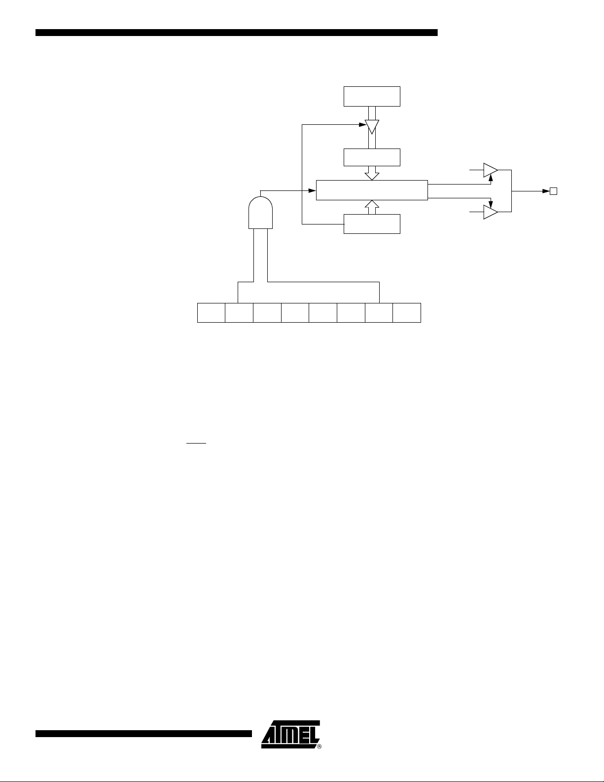
Figure 33. PCA PWM Mode
CL
CCAPnH
CCAPnL
ECOMn
CCAPMn, n = 0 to 4
0xDA to 0xDE
CAPNn MATn TOGn PWMn ECCFnCAPPn
8-bit Comparator
CEXn
“0”
“1”
≥
<
Enable
PCA Counter/Timer
Overflow
AT89C5131A-L
PCA Watchdog Timer
An on-board watchdog timer is available with the PCA to improve the reliability of the
system without increasing chip count. Watchdog timers are useful for systems that are
susceptible to noise, power glitches, or electrostatic discharge. Module 4 is the only
PCA module that can be programmed as a watchdog. However, this module can still be
used for other modes if the watchdog is not needed. Figure 31 shows a diagram of how
the watchdog works. The user pre-loads a 16-bit value in the compare registers. Just
like the other compare modes, this 16-bit value is compared to the PCA timer value. If a
match is allowed to occur, an internal reset will be generated. This will not cause the
RST pin to be driven low.
In order to hold off the reset, the user has three options:
1. Periodically change the compare value so it will never match the PCA timer
2. Periodically change the PCA timer value so it will never match the compare values, or
3. Disable the watchdog by clearing the WDTE bit before a match occurs and then
re-enable it
The first two options are more reliable because the watchdog timer is never disabled as
in option #3. If the program counter ever goes astray, a match will eventually occur and
cause an internal reset. The second option is also not recommended if other PCA modules are being used. Remember, the PCA timer is the time base for all modules;
changing the time base for other modules would not be a good idea. Thus, in most applications the first solution is the best option.
This watchdog timer won’t generate a reset out on the reset pin.
4338F–USB–08/07
65

AT89C5131A-L
Serial I/O Port
RITIRB8TB8RENSM2SM1SM0/FE
IDLPDGF0GF1POF-SMOD0SMOD1
To UART Framing Error Control
SM0 to UART Mode Control (SMOD0 = 0)
Set FE Bit if Stop Bit is 0 (framing error) (SMOD0 = 1)
SCON (98h)
PCON (87h)
Data Byte
RI
SMOD0 = X
Stop
Bit
Start
Bit
RXD
D7D6D5D4D3D2D1D0
FE
SMOD0 = 1
The serial I/O port in the AT89C5131A-L is compatible with the serial I/O port in the
80C52.
It provides both synchronous and asynchronous communication modes. It operates as
an Universal Asynchronous Receiver and Transmitter (UART) in three full-duplex
modes (modes 1, 2 and 3). Asynchronous transmission and reception can occur simultaneously and at different baud rates.
Serial I/O port includes the following enhancements:
• Framing error detection
• Automatic address recognition
Framing Error Detection
Framing bit error detection is provided for the three asynchronous modes (modes 1, 2
and 3). To enable the framing bit error detection feature, set SMOD0 bit in PCON register (see Figure 34).
Figure 34. Framing Error Block Diagram
When this feature is enabled, the receiver checks each incoming data frame for a valid
stop bit. An invalid stop bit may result from noise on the serial lines or from simultaneous
transmission by two CPUs. If a valid stop bit is not found, the Framing Error bit (FE) in
SCON register (See Table 56) bit is set.
Software may examine FE bit after each reception to check for data errors. Once set,
only software or a reset can clear FE bit. Subsequently received frames with valid stop
bits cannot clear FE bit. When FE feature is enabled, RI rises on stop bit instead of the
last data bit (See Figure 35 and Figure 36).
Figure 35. UART Timings in Mode 1
66
4338F–USB–08/07

Figure 36. UART Timings in Modes 2 and 3
RI
SMOD0 = 0
Data Byte Ninth
Bit
Stop
Bit
Start
Bit
RXD
D8D7D6D5D4D3D2D1D0
RI
SMOD0 = 1
FE
SMOD0 = 1
AT89C5131A-L
Automatic Address Recognition
The automatic address recognition feature is enabled when the multiprocessor communication feature is enabled (SM2 bit in SCON register is set).
Implemented in hardware, automatic address recognition enhances the multiprocessor
communication feature by allowing the serial port to examine the address of each
incoming command frame. Only when the serial port recognizes its own address, the
receiver sets RI bit in SCON register to generate an interrupt. This ensures that the CPU
is not interrupted by command frames addressed to other devices.
If desired, you may enable the automatic address recognition feature in mode 1. In this
configuration, the stop bit takes the place of the ninth data bit. Bit RI is set only when the
received command frame address matches the device’s address and is terminated by a
valid stop bit.
To support automatic address recognition, a device is identified by a given address and
a broadcast address.
Note: The multiprocessor communication and automatic address recognition features cannot
be enabled in mode 0 (i.e., setting SM2 bit in SCON register in mode 0 has no effect).
Given Address Each device has an individual address that is specified in SADDR register; the SADEN
register is a mask byte that contains don’t care bits (defined by zeros) to form the
device’s given address. The don’t care bits provide the flexibility to address one or more
slaves at a time. The following example illustrates how a given address is formed.
To address a device by its individual address, the SADEN mask byte must be 1111
1111b.
For example:
SADDR0101 0110b
SADEN1111 1100b
Given0101 01XXb
4338F–USB–08/07
The following is an example of how to use given addresses to address different slaves:
Slave A:SADDR1111 0001b
SADEN1111 1010b
Given1111 0X0Xb
Slave B:SADDR1111 0011b
SADEN1111 1001b
Given1111 0XX1b
Slave C:SADDR1111 0011b
SADEN1111 1101b
Given1111 00X1b
67

AT89C5131A-L
The SADEN byte is selected so that each slave may be addressed separately.
For slave A, bit 0 (the LSB) is a don’t care bit; for slaves B and C, bit 0 is a 1. To communicate with slave A only, the master must send an address where bit 0 is clear (e.g.
1111 0000b).
For slave A, bit 1 is a 1; for slaves B and C, bit 1 is a don’t care bit. To communicate with
slaves B and C, but not slave A, the master must send an address with bits 0 and 1 both
set (e.g. 1111 0011b).
To communicate with slaves A, B and C, the master must send an address with bit 0 set,
bit 1 clear, and bit 2 clear (e.g. 1111 0001b).
Broadcast Address A broadcast address is formed from the logical OR of the SADDR and SADEN registers
with zeros defined as don’t care bits, e.g.:
SADDR0101 0110b
SADEN1111 1100b
Broadcast = SADDR OR SADEN1111 111Xb
The use of don’t care bits provides flexibility in defining the broadcast address, in most
applications, a broadcast address is FFh. The following is an example of using broadcast addresses:
Slave A:SADDR1111 0001b
SADEN1111 1010b
Broadcast1111 1X11b,
Slave B:SADDR1111 0011b
SADEN1111 1001b
Broadcast1111 1X11B,
Slave C:SADDR = 1111 0011b
SADEN1111 1101b
Broadcast1111 1111b
For slaves A and B, bit 2 is a don’t care bit; for slave C, bit 2 is set. To communicate with
all of the slaves, the master must send an address FFh. To communicate with slaves A
and B, but not slave C, the master can send and address FBh.
Reset Addresses On reset, the SADDR and SADEN registers are initialized to 00h, i.e. the given and
broadcast addresses are XXXX XXXXb (all don’t care bits). This ensures that the serial
port will reply to any address, and so, that it is backwards compatible with the 80C51
microcontrollers that do not support automatic address recognition.
SADEN - Slave Address Mask Register (B9h)
7 6 5 4 3 2 1 0
Reset Value = 0000 0000b
Not bit addressable
68
4338F–USB–08/07

AT89C5131A-L
RCLK
/ 16
RBCK
INT_BRG
0
1
TIMER1
0
1
0
1
TIMER2
INT_BRG
TIMER1
TIMER2
TIMER_BRG_RX
Rx Clock
/ 16
0
1
TIMER_BRG_TX
Tx Clock
TBCK
TCLK
SADDR - Slave Address Register (A9h)
7 6 5 4 3 2 1 0
Reset Value = 0000 0000b
Not bit addressable
Baud Rate Selection for UART for Mode 1 and 3
Baud Rate Selection Table for
UART
The Baud Rate Generator for transmit and receive clocks can be selected separately via
the T2CON and BDRCON registers.
Figure 37. Baud Rate Selection
TCLK
(T2CON)
0 0 0 0 Timer 1 Timer 1
RCLK
(T2CON)
TBCK
(BDRCON)
RBCK
(BDRCON)
Clock Source
UART Tx
Clock Source
UART Rx
Internal Baud Rate Generator
(BRG)
4338F–USB–08/07
1 0 0 0 Timer 2 Timer 1
0 1 0 0 Timer 1 Timer 2
1 1 0 0 Timer 2 Timer 2
X 0 1 0 INT_BRG Timer 1
X 1 1 0 INT_BRG Timer 2
0 X 0 1 Timer 1 INT_BRG
1 X 0 1 Timer 2 INT_BRG
X X 1 1 INT_BRG INT_BRG
When the internal Baud Rate Generator is used, the Baud Rates are determined by the
BRG overflow depending on the BRL reload value, the value of SPD bit (Speed Mode)
in BDRCON register and the value of the SMOD1 bit in PCON register.
69

AT89C5131A-L
Figure 38. Internal Baud Rate
BRG
0
1
/6
BRL
/2
0
1
INT_BRG
SPD
BRR
SMOD1
auto reload counter
overflow
Peripheral Clock
Baud_Rate =
2
SMOD1
x FCLK PERIPH
2 x 6
(1-SPD)
x 16 x [256 - (BRL)]
(BRL) = 256
-
2
SMOD1
x F
CLK PERIPH
2 x 6
(1-SPD)
x 16 x Baud_Rate
• The baud rate for UART is token by formula:
70
4338F–USB–08/07

AT89C5131A-L
Table 56. SCON Register – SCON Serial Control Register (98h)
7 6 5 4 3 2 1 0
FE/SM0 SM1 SM2 REN TB8 RB8 TI RI
Bit
Number
7
6 SM1
5 SM2
4 REN
3 TB8
Bit
Mnemonic Description
Framing Error bit (SMOD0 = 1
FE
SM0
Clear to reset the error state, not cleared by a valid stop bit.
Set by hardware when an invalid stop bit is detected.
SMOD0 must be set to enable access to the FE bit
Serial port Mode bit 0
Refer to SM1 for serial port mode selection.
SMOD0 must be cleared to enable access to the SM0 bit
Serial port Mode bit 1
SM0SM1ModeDescriptionBaud Rate
0 0 0 Shift RegisterF
0 1 1 8-bit UARTVariable
1 0 2 9-bit UARTF
1 1 3 9-bit UART Variable
Serial port Mode 2 bit/Multiprocessor Communication Enable bit
Clear to disable multiprocessor communication feature.
Set to enable multiprocessor communication feature in mode 2 and 3, and
eventually mode 1. This bit should be cleared in mode 0.
Reception Enable bit
Clear to disable serial reception.
Set to enable serial reception.
Transmitter Bit 8/Ninth bit to Transmit in Modes 2 and 3
Clear to transmit a logic 0 in the 9th bit.
Set to transmit a logic 1 in the 9th bit.
CPU PERIPH
CPU PERIPH/
)
/6
32 or/16
Receiver Bit 8/Ninth bit received in modes 2 and 3
2 RB8
1 TI
0 RI
Cleared by hardware if 9th bit received is a logic 0.
Set by hardware if 9th bit received is a logic 1.
In mode 1, if SM2 = 0, RB8 is the received stop bit. In mode 0 RB8 is not used.
Transmit Interrupt flag
Clear to acknowledge interrupt.
Set by hardware at the end of the 8th bit time in mode 0 or at the beginning of the
stop bit in the other modes.
Receive Interrupt flag
Clear to acknowledge interrupt.
Set by hardware at the end of the 8th bit time in mode 0, see Figure 35. and
Figure 36. in the other modes.
Reset Value = 0000 0000b
Bit addressable
4338F–USB–08/07
71

AT89C5131A-L
Example of computed value when X2 = 1, SMOD1 = 1, SPD = 1
F
= 16.384 MHz F
Baud Rates
115200 247 1.23 243 0.16
57600 238 1.23 230 0.16
38400 229 1.23 217 0.16
28800 220 1.23 204 0.16
19200 203 0.63 178 0.16
9600 149 0.31 100 0.16
4800 43 1.23 - -
OSC
BRL Error (%) BRL Error (%)
OSC
Example of computed value when X2 = 0, SMOD1 = 0, SPD = 0
F
= 16.384 MHz F
OSC
Baud Rates
4800 247 1.23 243 0.16
2400 238 1.23 230 0.16
1200 220 1.23 202 3.55
BRL Error (%) BRL Error (%)
OSC
= 24 MHz
= 24 MHz
UART Registers
600 185 0.16 152 0.16
The baud rate generator can be used for mode 1 or 3 (refer to Figure 37.), but also for
mode 0 for UART, thanks to the bit SRC located in BDRCON register (Table 59.)
SADEN - Slave Address Mask Register for UART (B9h)
7 6 5 4 3 2 1 0
– – – – – – – –
Reset Value = 0000 0000b
SADDR - Slave Address Register for UART (A9h)
7 6 5 4 3 2 1 0
– – – – – – – –
Reset Value = 0000 0000b
SBUF - Serial Buffer Register for UART (99h)
7 6 5 4 3 2 1 0
– – – – – – – –
Reset Value = XXXX XXXXb
72
4338F–USB–08/07

AT89C5131A-L
BRL - Baud Rate Reload Register for the internal baud rate generator, UART (9Ah)
7 6 5 4 3 2 1 0
– – – – – – – –
Reset Value = 0000 0000b
Table 57. T2CON Register
T2CON - Timer 2 Control Register (C8h)
7 6 5 4 3 2 1 0
TF2 EXF2 RCLK TCLK EXEN2 TR2 C/T2# CP/RL2#
Bit
Number
7 TF2
6 EXF2
5 RCLK
4 TCLK
3 EXEN2
2 TR2
Bit
Mnemonic Description
Timer 2 overflow Flag
Must be cleared by software.
Set by hardware on Timer 2 overflow, if RCLK = 0 and TCLK = 0.
Timer 2 External Flag
Set when a capture or a reload is caused by a negative transition on T2EX pin if
EXEN2 = 1.
When set, causes the CPU to vector to Timer 2 interrupt routine when Timer 2
interrupt is enabled.
Must be cleared by software. EXF2 doesn’t cause an interrupt in Up/down
counter mode (DCEN = 1)
Receive Clock bit for UART
Cleared to use Timer 1 overflow as receive clock for serial port in mode 1 or 3.
Set to use Timer 2 overflow as receive clock for serial port in mode 1 or 3.
Transmit Clock bit for UART
Cleared to use Timer 1 overflow as transmit clock for serial port in mode 1 or 3.
Set to use Timer 2 overflow as transmit clock for serial port in mode 1 or 3.
Timer 2 External Enable bit
Cleared to ignore events on T2EX pin for Timer 2 operation.
Set to cause a capture or reload when a negative transition on T2EX pin is
detected, if Timer 2 is not used to clock the serial port.
Timer 2 Run control bit
Cleared to turn off Timer 2.
Set to turn on Timer 2.
4338F–USB–08/07
Timer/Counter 2 select bit
1 C/T2#
0 CP/RL2#
Cleared for timer operation (input from internal clock system: F
Set for counter operation (input from T2 input pin, falling edge trigger). Must be 0
for clock out mode.
Timer 2 Capture/Reload bit
If RCLK = 1 or TCLK = 1, CP/RL2# is ignored and timer is forced to Auto-reload
on Timer 2 overflow.
Cleared to Auto-reload on Timer 2 overflows or negative transitions on T2EX pin
if EXEN2 = 1.
Set to capture on negative transitions on T2EX pin if EXEN2 = 1.
Reset Value = 0000 0000b
Bit addressable
CLK PERIPH
).
73

AT89C5131A-L
Table 58. PCON Register
PCON - Power Control Register (87h)
7 6 5 4 3 2 1 0
SMOD1 SMOD0 - POF GF1 GF0 PD IDL
Bit
Number
7 SMOD1
6 SMOD0
5 -
4 POF
3 GF1
2 GF0
1 PD
0 IDL
Bit
Mnemonic Description
Serial port Mode bit 1 for UART
Set to select double baud rate in mode 1, 2 or 3.
Serial port Mode bit 0 for UART
Cleared to select SM0 bit in SCON register.
Set to select FE bit in SCON register.
Reserved
The value read from this bit is indeterminate. Do not set this bit.
Power-Off Flag
Cleared to recognize next reset type.
Set by hardware when VCC rises from 0 to its nominal voltage. Can also be set by
software.
General-purpose Flag
Cleared by user for general-purpose usage.
Set by user for general-purpose usage.
General-purpose Flag
Cleared by user for general-purpose usage.
Set by user for general-purpose usage.
Power-down Mode Bit
Cleared by hardware when reset occurs.
Set to enter power-down mode.
Idle Mode Bit
Cleared by hardware when interrupt or reset occurs.
Set to enter idle mode.
74
Reset Value = 00X1 0000b
Not bit addressable
Power-off flag reset value will be 1 only after a power on (cold reset). A warm reset
doesn’t affect the value of this bit.
4338F–USB–08/07

AT89C5131A-L
Table 59. BDRCON Register
BDRCON - Baud Rate Control Register (9Bh)
7 6 5 4 3 2 1 0
- - - BRR TBCK RBCK SPD SRC
Bit
Number
7 -
6 -
5 -
4 BRR
3 TBCK
2 RBCK
1 SPD
0 SRC
Bit
Mnemonic Description
Reserved
The value read from this bit is indeterminate. Do not set this bit
Reserved
The value read from this bit is indeterminate. Do not set this bit
Reserved
The value read from this bit is indeterminate. Do not set this bit.
Baud Rate Run Control bit
Cleared to stop the internal Baud Rate Generator.
Set to start the internal Baud Rate Generator.
Transmission Baud rate Generator Selection bit for UART
Cleared to select Timer 1 or Timer 2 for the Baud Rate Generator.
Set to select internal Baud Rate Generator.
Reception Baud Rate Generator Selection bit for UART
Cleared to select Timer 1 or Timer 2 for the Baud Rate Generator.
Set to select internal Baud Rate Generator.
Baud Rate Speed Control bit for UART
Cleared to select the SLOW Baud Rate Generator.
Set to select the FAST Baud Rate Generator.
Baud Rate Source select bit in Mode 0 for UART
Cleared to select F
mode).
Set to select the internal Baud Rate Generator for UARTs in mode 0.
/12 as the Baud Rate Generator (F
OSC
CLK PERIPH
/6 in X2
4338F–USB–08/07
Reset Value = XXX0 0000b
Not bit addressable
75

AT89C5131A-L
Interrupt System
IE1
0
3
High priority
interrupt
Interrupt
Polling
Sequence, Decreasing From
High-to-Low Priority
Low Priority
Interrupt
Global DisableIndividual Enable
EXF2
TF2
TI
RI
TF0
INT0
INT1
TF1
IPH, IPL
IE0
0
3
0
3
0
3
0
3
0
3
0
3
PCA IT
KBD IT
SPI IT
0
3
0
3
0
3
UEPINT
USBINT
0
3
TWI IT
1
1
0
0
IT0
TCON.0
IT1
TCON.2
Overview
Figure 39. Interrupt Control System
The AT89C5131A-L has a total of 11 interrupt vectors: two external interrupts (INT0 and
INT1), three timer interrupts (timers 0, 1 and 2), the serial port interrupt, SPI interrupt,
Keyboard interrupt, USB interrupt and the PCA global interrupt. These interrupts are
shown in Figure 39.
76
4338F–USB–08/07

AT89C5131A-L
Each of the interrupt sources can be individually enabled or disabled by setting or clearing a bit in the Interrupt Enable register (Table 61). This register also contains a global
disable bit, which must be cleared to disable all interrupts at once.
Each interrupt source can also be individually programmed to one out of four priority levels by setting or clearing a bit in the Interrupt Priority register (Table 62.) and in the
Interrupt Priority High register (Table 63). Table 60. shows the bit values and priority levels associated with each combination.
Registers
The PCA interrupt vector is located at address 0033H, the SPI interrupt vector is located
at address 004BH and Keyboard interrupt vector is located at address 003BH. All other
vectors addresses are the same as standard C52 devices.
Table 60. Priority Level Bit Values
IPH.x IPL.x Interrupt Level Priority
0 0 0 (Lowest)
0 1 1
1 0 2
1 1 3 (Highest)
A low-priority interrupt can be interrupted by a high priority interrupt, but not by another
low-priority interrupt. A high-priority interrupt can’t be interrupted by any other interrupt
source.
If two interrupt requests of different priority levels are received simultaneously, the
request of higher priority level is serviced. If interrupt requests of the same priority level
are received simultaneously, an internal polling sequence determines which request is
serviced. Thus within each priority level there is a second priority structure determined
by the polling sequence.
4338F–USB–08/07
77

AT89C5131A-L
Table 61. IEN0 Register
IEN0 - Interrupt Enable Register (A8h)
7 6 5 4 3 2 1 0
EA EC ET2 ES ET1 EX1 ET0 EX0
Bit
Number
7 EA
6 EC
5 ET2
4 ES
3 ET1
2 EX1
1 ET0
Bit
Mnemonic Description
Enable All interrupt bit
Cleared to disable all interrupts.
Set to enable all interrupts.
PCA interrupt enable bit
Cleared to disable.
Set to enable.
Timer 2 overflow interrupt Enable bit
Cleared to disable Timer 2 overflow interrupt.
Set to enable Timer 2 overflow interrupt.
Serial port Enable bit
Cleared to disable serial port interrupt.
Set to enable serial port interrupt.
Timer 1 overflow interrupt Enable bit
Cleared to disable Timer 1 overflow interrupt.
Set to enable Timer 1 overflow interrupt.
External interrupt 1 Enable bit
Cleared to disable external interrupt 1.
Set to enable external interrupt 1.
Timer 0 overflow interrupt Enable bit
Cleared to disable timer 0 overflow interrupt.
Set to enable timer 0 overflow interrupt.
0 EX0
External interrupt 0 Enable bit
Cleared to disable external interrupt 0.
Set to enable external interrupt 0.
Reset Value = 0000 0000b
Bit addressable
78
4338F–USB–08/07

AT89C5131A-L
Table 62. IPL0 Register
IPL0 - Interrupt Priority Register (B8h)
7 6 5 4 3 2 1 0
- PPCL PT2L PSL PT1L PX1L PT0L PX0L
Bit
Number
7 -
6 PPCL
5 PT2L
4 PSL
3 PT1L
2 PX1L
1 PT0L
0 PX0L
Bit
Mnemonic Description
Reserved
The value read from this bit is indeterminate. Do not set this bit.
PCA interrupt Priority bit
Refer to PPCH for priority level.
Timer 2 overflow interrupt Priority bit
Refer to PT2H for priority level.
Serial port Priority bit
Refer to PSH for priority level.
Timer 1 overflow interrupt Priority bit
Refer to PT1H for priority level.
External interrupt 1 Priority bit
Refer to PX1H for priority level.
Timer 0 overflow interrupt Priority bit
Refer to PT0H for priority level.
External interrupt 0 Priority bit
Refer to PX0H for priority level.
Reset Value = X000 0000b
Bit addressable
4338F–USB–08/07
79

AT89C5131A-L
Table 63. IPH0 Register
IPH0 - Interrupt Priority High Register (B7h)
7 6 5 4 3 2 1 0
- PPCH PT2H PSH PT1H PX1H PT0H PX0H
Bit
Number
7 -
6 PPCH
5 PT2H
4 PSH
3 PT1H
Bit
Mnemonic Description
Reserved
The value read from this bit is indeterminate. Do not set this bit.
PCA interrupt Priority high bit.
PPCHPPCLPriority Level
0 0Lowest
0 1
1 0
1 1Highest
Timer 2 overflow interrupt Priority High bit
PT2HPT2LPriority Level
0 0Lowest
0 1
1 0
1 1Highest
Serial port Priority High bit
PSHPSLPriority Level
0 0Lowest
0 1
1 0
1 1Highest
Timer 1 overflow interrupt Priority High bit
PT1HPT1LPriority Level
0 0Lowest
0 1
1 0
1 1Highest
80
External interrupt 1 Priority High bit
PX1HPX1LPriority Level
2 PX1H
1 PT0H
0 PX0H
0 0Lowest
0 1
1 0
1 1Highest
Timer 0 overflow interrupt Priority High bit
PT0HPT0LPriority Level
0 0Lowest
0 1
1 0
1 1Highest
External interrupt 0 Priority High bit
PX0HPX0LPriority Level
0 0Lowest
0 1
1 0
1 1Highest
Reset Value = X000 0000b
Not bit addressable
4338F–USB–08/07

AT89C5131A-L
Table 64. IEN1 Register
IEN1 - Interrupt Enable Register (B1h)
7 6 5 4 3 2 1 0
- EUSB - - - ESPI ETWI EKB
Bit
Number
7 - Reserved
6 EUSB
5 - Reserved
4 - Reserved
3 - Reserved
2 ESPI
1 ETWI
0 EKB
Bit
Mnemonic Description
USB Interrupt Enable bit
Cleared to disable USB interrupt.
Set to enable USB interrupt.
SPI interrupt Enable bit
Cleared to disable SPI interrupt.
Set to enable SPI interrupt.
TWI interrupt Enable bit
Cleared to disable TWI interrupt.
Set to enable TWI interrupt.
Keyboard interrupt Enable bit
Cleared to disable keyboard interrupt.
Set to enable keyboard interrupt.
Reset Value = X0XX X000b
Not bit addressable
4338F–USB–08/07
81

AT89C5131A-L
Table 65. IPL1 Register
IPL1 - Interrupt Priority Register (B2h)
7 6 5 4 3 2 1 0
- PUSBL - - - PSPIL PTWIL PKBDL
Bit
Number
7 -
6 PUSBL
5 -
4 -
3 -
2 PSPIL
1 PTWIL
0 PKBL
Bit
Mnemonic Description
Reserved
The value read from this bit is indeterminate. Do not set this bit.
USB Interrupt Priority bit
Refer to PUSBH for priority level.
Reserved
The value read from this bit is indeterminate. Do not set this bit.
Reserved
The value read from this bit is indeterminate. Do not set this bit.
Reserved
The value read from this bit is indeterminate. Do not set this bit.
SPI Interrupt Priority bit
Refer to PSPIH for priority level.
TWI Interrupt Priority bit
Refer to PTWIH for priority level.
Keyboard Interrupt Priority bit
Refer to PKBH for priority level.
Reset Value = X0XX X000b
Not bit addressable
82
4338F–USB–08/07

AT89C5131A-L
Table 66. IPH1 Register
IPH1 - Interrupt Priority High Register (B3h)
7 6 5 4 3 2 1 0
- PUSBH - - - PSPIH PTWIH PKBH
Bit
Number
7 -
6 PUSBH
5 -
4 -
3 -
2 PSPIH
1 PTWIH
Bit
Mnemonic Description
Reserved
The value read from this bit is indeterminate. Do not set this bit.
USB Interrupt Priority High bit
PUSBHPUSBLPriority Level
0 0Lowest
0 1
1 0
1 1Highest
Reserved
The value read from this bit is indeterminate. Do not set this bit.
Reserved
The value read from this bit is indeterminate. Do not set this bit.
Reserved
The value read from this bit is indeterminate. Do not set this bit.
SPI Interrupt Priority High bit
PSPIHPSPILPriority Level
0 0Lowest
0 1
1 0
1 1Highest
TWI Interrupt Priority High bit
PTWIHPTWILPriority Level
0 0Lowest
0 1
1 0
1 1Highest
4338F–USB–08/07
Keyboard Interrupt Priority High bit
PKBHPKBLPriority Level
0 PKBH
0 0Lowest
0 1
1 0
1 1Highest
Reset Value = X0XX X000b
Not bit addressable
83

AT89C5131A-L
Interrupt Sources and Vector Addresses
Table 67. Vector Table
Number
0 0 Reset 0000h
1 1 INT0 IE0 0003h
2 2 Timer 0 TF0 000Bh
3 3 INT1 IE1 0013h
4 4 Timer 1 IF1 001Bh
5 6 UART RI+TI 0023h
6 7 Timer 2 TF2+EXF2 002Bh
7 5 PCA CF + CCFn (n = 0-4) 0033h
8 8 Keyboard KBDIT 003Bh
9 9 TWI TWIIT 0043h
10 10 SPI SPIIT 004Bh
11 11 0053h
12 12 005Bh
13 13 0063h
Polling
Priority
Interrupt
Source
Interrupt
Request
Vector
Address
14 14 USB UEPINT + USBINT 006Bh
15 15 0073h
84
4338F–USB–08/07
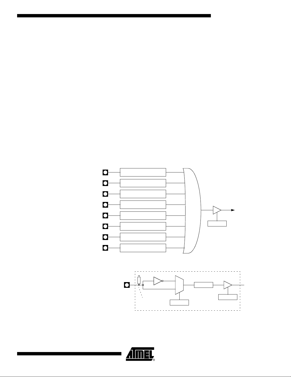
Keyboard Interface
P1.0
Keyboard Interface
Interrupt Request
KBD
IE1.0
Input Circuitry
P1.1 Input Circuitry
P1.2 Input Circuitry
P1.3 Input Circuitry
P1.4 Input Circuitry
P1.5 Input Circuitry
P1.6 Input Circuitry
P1.7 Input Circuitry
KBDIT
P1:x
KBE.x
KBF.x
KBLS.x
0
1
Vcc
Internal Pull-up
AT89C5131A-L
Introduction
The AT89C5131A-L implements a keyboard interface allowing the connection of a 8 x n
matrix keyboard. It is based on 8 inputs with programmable interrupt capability on both
high or low level. These inputs are available as an alternate function of P1 and allow to
exit from idle and power down modes.
Description
The keyboard interface communicates with the C51 core through 3 special function registers: KBLS, the Keyboard Level Selection register (Table 70), KBE, The Keyboard
interrupt Enable register (Table 69), and KBF, the Keyboard Flag register (Table 68).
Interrupt The keyboard inputs are considered as 8 independent interrupt sources sharing the
same interrupt vector. An interrupt enable bit (KBD in IE1) allows global enable or disable of the keyboard interrupt (see Figure 40). As detailed in Figure 41 each keyboard
input has the capability to detect a programmable level according to KBLS.x bit value.
Level detection is then reported in interrupt flags KBF.x that can be masked by software
using KBE.x bits.
This structure allow keyboard arrangement from 1 by n to 8 by n matrix and allow usage
of P1 inputs for other purpose.
Figure 40. Keyboard Interface Block Diagram
4338F–USB–08/07
Figure 41. Keyboard Input Circuitry
85

AT89C5131A-L
Power Reduction Mode P1 inputs allow exit from idle and power down modes as detailed in section “Power-
down Mode”.
Registers
Table 68. KBF Register
KBF - Keyboard Flag Register (9Eh)
7 6 5 4 3 2 1 0
KBF7 KBF6 KBF5 KBF4 KBF3 KBF2 KBF1 KBF0
Bit
Number
7 KBF7
6 KBF6
5 KBF5
4 KBF4
Bit
Mnemonic Description
Keyboard line 7 flag
Set by hardware when the Port line 7 detects a programmed level. It generates a
Keyboard interrupt request if the KBKBIE.7 bit in KBIE register is set.
Cleared by hardware when reading KBF SFR by software.
Keyboard line 6 flag
Set by hardware when the Port line 6 detects a programmed level. It generates a
Keyboard interrupt request if the KBIE.6 bit in KBIE register is set.
Cleared by hardware when reading KBF SFR by software.
Keyboard line 5 flag
Set by hardware when the Port line 5 detects a programmed level. It generates a
Keyboard interrupt request if the KBIE.5 bit in KBIE register is set.
Cleared by hardware when reading KBF SFR by software.
Keyboard line 4 flag
Set by hardware when the Port line 4 detects a programmed level. It generates a
Keyboard interrupt request if the KBIE.4 bit in KBIE register is set.
Cleared by hardware when reading KBF SFR by software.
Keyboard line 3 flag
3 KBF3
2 KBF2
1 KBF1
0 KBF0
Set by hardware when the Port line 3 detects a programmed level. It generates a
Keyboard interrupt request if the KBIE.3 bit in KBIE register is set.
Cleared by hardware when reading KBF SFR by software.
Keyboard line 2 flag
Set by hardware when the Port line 2 detects a programmed level. It generates a
Keyboard interrupt request if the KBIE.2 bit in KBIE register is set.
Must be cleared by software.
Keyboard line 1 flag
Set by hardware when the Port line 1 detects a programmed level. It generates a
Keyboard interrupt request if the KBIE.1 bit in KBIE register is set.
Cleared by hardware when reading KBF SFR by software.
Keyboard line 0 flag
Set by hardware when the Port line 0 detects a programmed level. It generates a
Keyboard interrupt request if the KBIE.0 bit in KBIE register is set.
Cleared by hardware when reading KBF SFR by software.
Reset Value = 0000 0000b
86
4338F–USB–08/07

AT89C5131A-L
Table 69. KBE Register
KBE - Keyboard Input Enable Register (9Dh)
7 6 5 4 3 2 1 0
KBE7 KBE6 KBE5 KBE4 KBE3 KBE2 KBE1 KBE0
Bit
Number
7 KBE7
6 KBE6
5 KBE5
4 KBE4
3 KBE3
2 KBE2
1 KBE1
Bit
Mnemonic Description
Keyboard line 7 Enable bit
Cleared to enable standard I/O pin.
Set to enable KBF.7 bit in KBF register to generate an interrupt request.
Keyboard line 6 Enable bit
Cleared to enable standard I/O pin.
Set to enable KBF.6 bit in KBF register to generate an interrupt request.
Keyboard line 5 Enable bit
Cleared to enable standard I/O pin.
Set to enable KBF.5 bit in KBF register to generate an interrupt request.
Keyboard line 4 Enable bit
Cleared to enable standard I/O pin.
Set to enable KBF.4 bit in KBF register to generate an interrupt request.
Keyboard line 3 Enable bit
Cleared to enable standard I/O pin.
Set to enable KBF.3 bit in KBF register to generate an interrupt request.
Keyboard line 2 Enable bit
Cleared to enable standard I/O pin.
Set to enable KBF.2 bit in KBF register to generate an interrupt request.
Keyboard line 1 Enable bit
Cleared to enable standard I/O pin.
Set to enable KBF.1 bit in KBF register to generate an interrupt request.
0 KBE0
Keyboard line 0 Enable bit
Cleared to enable standard I/O pin.
Set to enable KBF.0 bit in KBF register to generate an interrupt request.
Reset Value = 0000 0000b
4338F–USB–08/07
87

AT89C5131A-L
Table 70. KBLS Register
KBLS-Keyboard Level Selector Register (9Ch)
7 6 5 4 3 2 1 0
KBLS7 KBLS6 KBLS5 KBLS4 KBLS3 KBLS2 KBLS1 KBLS0
Bit
Number
7 KBLS7
6 KBLS6
5 KBLS5
4 KBLS4
3 KBLS3
2 KBLS2
1 KBLS1
Bit
Mnemonic Description
Keyboard line 7 Level Selection bit
Cleared to enable a low level detection on Port line 7.
Set to enable a high level detection on Port line 7.
Keyboard line 6 Level Selection bit
Cleared to enable a low level detection on Port line 6.
Set to enable a high level detection on Port line 6.
Keyboard line 5 Level Selection bit
Cleared to enable a low level detection on Port line 5.
Set to enable a high level detection on Port line 5.
Keyboard line 4 Level Selection bit
Cleared to enable a low level detection on Port line 4.
Set to enable a high level detection on Port line 4.
Keyboard line 3 Level Selection bit
Cleared to enable a low level detection on Port line 3.
Set to enable a high level detection on Port line 3.
Keyboard line 2 Level Selection bit
Cleared to enable a low level detection on Port line 2.
Set to enable a high level detection on Port line 2.
Keyboard line 1 Level Selection bit
Cleared to enable a low level detection on Port line 1.
Set to enable a high level detection on Port line 1.
0 KBLS0
Keyboard line 0 Level Selection bit
Cleared to enable a low level detection on Port line 0.
Set to enable a high level detection on Port line 0.
Reset Value = 0000 0000b
88
4338F–USB–08/07

AT89C5131A-L
Programmable LED
AT89C5131A-L have up to 4 programmable LED current sources, configured by the
register LEDCON.
Table 71. LEDCON Register
LEDCON (S:F1h) LED Control Register
7 6 5 4 3 2 1 0
LED3 LED2 LED1 LED0
Bit
Number
7:6 LED3
5:4 LED2
3:2 LED1
Bit
Mnemonic Description
PortLED3Configuration
0 0Standard C51 Port
0 1 2 mA current source when P3.7 is low
1 0 4 mA current source when P3.7 is low
1 1 10 mA current source when P3.7 is low
Port/LED2Configuration
0 0 Standard C51 Port
0 1 2 mA current source when P3.6 is low
1 0 4 mA current source when P3.6 is low
1 1 10 mA current source when P3.6 is low
Port/LED1Configuration
0 0 Standard C51 Port
0 1 2 mA current source when P3.5 is low
1 0 4 mA current source when P3.5 is low
1 1 10 mA current source when P3.5 is low
1:0 LED0
Reset Value = 00h
Port/LED0Configuration
0 0 Standard C51 Port
0 1 2 mA current source when P3.3 is low
1 0 4 mA current source when P3.3 is low
1 1 10 mA current source when P3.3 is low
4338F–USB–08/07
89

AT89C5131A-L
Serial Peripheral
Slave 1
MISO
MOSI
SCK
SS
MISO
MOSI
SCK
SS
PORT
0
1
2
3
Slave 3
MISO
MOSI
SCK
SS
Slave 4
MISO
MOSI
SCK
SS
Slave 2
MISO
MOSI
SCK
SS
VDD
Master
Interface (SPI)
The Serial Peripheral Interface module (SPI) allows full-duplex, synchronous, serial
communication between the MCU and peripheral devices, including other MCUs.
Features
Signal Description
Features of the SPI module include the following:
• Full-duplex, three-wire synchronous transfers
• Master or Slave operation
• Eight programmable Master clock rates
• Serial clock with programmable polarity and phase
• Master mode fault error flag with MCU interrupt capability
• Write collision flag protection
Figure 42 shows a typical SPI bus configuration using one Master controller and many
Slave peripherals. The bus is made of three wires connecting all the devices:
Figure 42. SPI Master/Slaves Interconnection
Master Output Slave Input
(MOSI)
Master Input Slave Output
(MISO)
SPI Serial Clock (SCK) This signal is used to synchronize the data movement both in and out the devices
Slave Select (SS) Each Slave peripheral is selected by one Slave Select pin (SS). This signal must stay
90
The Master device selects the individual Slave devices by using four pins of a parallel
port to control the four SS pins of the Slave devices.
This 1-bit signal is directly connected between the Master Device and a Slave Device.
The MOSI line is used to transfer data in series from the Master to the Slave. Therefore,
it is an output signal from the Master, and an input signal to a Slave. A byte (8-bit word)
is transmitted most significant bit (MSB) first, least significant bit (LSB) last.
This 1-bit signal is directly connected between the Slave Device and a Master Device.
The MISO line is used to transfer data in series from the Slave to the Master. Therefore,
it is an output signal from the Slave, and an input signal to the Master. A byte (8-bit
word) is transmitted most significant bit (MSB) first, least significant bit (LSB) last.
through their MOSI and MISO lines. It is driven by the Master for eight clock cycles
which allows to exchange one byte on the serial lines.
low for any message for a Slave. It is obvious that only one Master (SS high level) can
drive the network. The Master may select each Slave device by software through port
4338F–USB–08/07

AT89C5131A-L
pins (Figure 42). To prevent bus conflicts on the MISO line, only one slave should be
selected at a time by the Master for a transmission.
In a Master configuration, the SS line can be used in conjunction with the MODF flag in
the SPI Status register (SPSTA) to prevent multiple masters from driving MOSI and
SCK (see Section “Error Conditions”, page 95).
A high level on the SS pin puts the MISO line of a Slave SPI in a high-impedance state.
The SS pin could be used as a general-purpose if the following conditions are met:
• The device is configured as a Master and the SSDIS control bit in SPCON is set.
This kind of configuration can be found when only one Master is driving the network
and there is no way that the SS pin could be pulled low. Therefore, the MODF flag in
the SPSTA will never be set
• The Device is configured as a Slave with CPHA and SSDIS control bits set
kind of configuration can happen when the system comprises one Master and one
Slave only. Therefore, the device should always be selected and there is no reason
that the Master uses the SS pin to select the communicating Slave device.
Notes: 1. Clearing SSDIS control bit does not clear MODF.
2. Special care should be taken not to set SSDIS control bit when CPHA =’0’ because in
this mode, the SS is used to start the transmission.
(1)
.
(2)
This
Baud Rate In Master mode, the baud rate can be selected from a baud rate generator which is con-
trolled by three bits in the SPCON register: SPR2, SPR1 and SPR0. The Master clock is
chosen from one of seven clock rates resulting from the division of the internal clock by
2, 4, 8, 16, 32, 64 or 128.
Table 72 gives the different clock rates selected by SPR2:SPR1:SPR0:
Table 72. SPI Master Baud Rate Selection
SPR2 SPR1 SPR0 Clock Rate Baud Rate Divisor (BD)
0 0 0 Don’t Use No BRG
0 0 1 F
0 1 0 F
0 1 1 F
1 0 0 F
1 0 1 F
1 1 0 F
1 1 1 Don’t Use No BRG
CLK PERIPH
CLK PERIPH
CLK PERIPH
CLK PERIPH
CLK PERIPH
CLK PERIPH
/4 4
/8 8
/16 16
/32 32
/64 64
/128 128
4338F–USB–08/07
91

AT89C5131A-L
Functional Description
Shift Register
01
234567
Internal Bus
Pin
Control
Logic
MISO
MOSI
SCK
M
S
Clock
Logic
Clock
Divider
Clock
Select
/4
/64
/128
SPI Interrupt Request
8-bit bus
1-bit signal
SS
FCLK PERIPH
/32
/8
/16
Receive Data Register
SPDAT
SPI
Control
SPSTA
CPHA
SPR0
SPR1
CPOLMSTRSSDISSPEN
SPR2
SPCON
WCOL MODFSPIF
- - - -
SSERR
Figure 43 shows a detailed structure of the SPI module.
Figure 43. SPI Module Block Diagram
Operating Modes The Serial Peripheral Interface can be configured as one of the two modes: Master
92
mode or Slave mode. The configuration and initialization of the SPI module is made
through one register:
• The Serial Peripheral CONtrol register (SPCON)
Once the SPI is configured, the data exchange is made using:
• SPCON
• The Serial Peripheral STAtus register (SPSTA)
• The Serial Peripheral DATa register (SPDAT)
During an SPI transmission, data is simultaneously transmitted (shifted out serially) and
received (shifted in serially). A serial clock line (SCK) synchronizes shifting and sampling on the two serial data lines (MOSI and MISO). A Slave Select line (SS) allows
individual selection of a Slave SPI device; Slave devices that are not selected do not
interfere with SPI bus activities.
When the Master device transmits data to the Slave device via the MOSI line, the Slave
device responds by sending data to the Master device via the MISO line. This implies
full-duplex transmission with both data out and data in synchronized with the same clock
(Figure 44).
4338F–USB–08/07

Figure 44. Full-duplex Master/Slave Interconnection
8-bit Shift Register
SPI
Clock Generator
Master MCU
8-bit Shift Register
MISOMISO
MOSI
MOSI
SCK SCK
VSS
VDD
SSSS
Slave MCU
AT89C5131A-L
Master Mode The SPI operates in Master mode when the Master bit, MSTR
is set. Only one Master SPI device can initiate transmissions. Software begins the transmission from a Master SPI module by writing to the Serial Peripheral Data Register
(SPDAT). If the shift register is empty, the byte is immediately transferred to the shift
register. The byte begins shifting out on MOSI pin under the control of the serial clock,
SCK. Simultaneously, another byte shifts in from the Slave on the Master’s MISO pin.
The transmission ends when the Serial Peripheral transfer data flag, SPIF, in SPSTA
becomes set. At the same time that SPIF becomes set, the received byte from the Slave
is transferred to the receive data register in SPDAT. Software clears SPIF by reading
the Serial Peripheral Status register (SPSTA) with the SPIF bit set, and then reading the
SPDAT.
Slave Mode The SPI operates in Slave mode when the Master bit, MSTR
(2)
cleared. Before a data transmission occurs, the Slave Select pin, SS, of the Slave
device must be set to’0’. SS must remain low until the transmission is complete.
In a Slave SPI module, data enters the shift register under the control of the SCK from
the Master SPI module. After a byte enters the shift register, it is immediately transferred
to the receive data register in SPDAT, and the SPIF bit is set. To prevent an overflow
condition, Slave software must then read the SPDAT before another byte enters the
shift register
(3)
. A Slave SPI must complete the write to the SPDAT (shift register) at
least one bus cycle before the Master SPI starts a transmission. If the write to the data
register is late, the SPI transmits the data already in the shift register from the previous
transmission.
(1)
, in the SPCON register
, in the SPCON register is
Transmission Formats Software can select any of four combinations of serial clock (SCK) phase and polarity
using two bits in the SPCON: the Clock POLarity (CPOL
(4)
) and the Clock PHAse
(CPHA4). CPOL defines the default SCK line level in idle state. It has no significant
effect on the transmission format. CPHA defines the edges on which the input data are
sampled and the edges on which the output data are shifted (Figure 45 and Figure 46).
The clock phase and polarity should be identical for the Master SPI device and the communicating Slave device.
1. The SPI module should be configured as a Master before it is enabled (SPEN set). Also
the Master SPI should be configured before the Slave SPI.
2. The SPI module should be configured as a Slave before it is enabled (SPEN set).
3. The maximum frequency of the SCK for an SPI configured as a Slave is the bus clock
speed.
4338F–USB–08/07
4. Before writing to the CPOL and CPHA bits, the SPI should be disabled (SPEN =’0’).
93

AT89C5131A-L
Figure 45. Data Transmission Format (CPHA = 0)
MSB bit6 bit5 bit4 bit3 bit2 bit1 LSB
bit6 bit5 bit4 bit3 bit2 bit1MSB LSB
1 32 4 5 6 7 8
Capture point
SS (to Slave)
MISO (from Slave)
MOSI (from Master)
SCK (CPOL = 1)
SCK (CPOL = 0)
SPEN (internal)
SCK cycle number
MSB bit6 bit5 bit4 bit3 bit2 bit1 LSB
bit6 bit5 bit4 bit3 bit2 bit1
MSB LSB
1 32 4 5 6 7 8
Capture point
SS (to Slave)
MISO (from Slave)
MOSI (from Master)
SCK (CPOL = 1)
SCK (CPOL = 0)
SPEN (internal)
SCK cycle number
Byte 1 Byte 2
Byte 3
MISO/MOSI
Master SS
Slave SS
(CPHA = 1)
Slave SS
(CPHA = 0)
Figure 46. Data Transmission Format (CPHA = 1)
Figure 47. CPHA/SS Timing
94
As shown in Figure 46, the first SCK edge is the MSB capture strobe. Therefore the
Slave must begin driving its data before the first SCK edge, and a falling edge on the SS
pin is used to start the transmission. The SS pin must be toggled high and then low
between each byte transmitted (Figure 43).
Figure 47 shows an SPI transmission in which CPHA is’1’. In this case, the Master
begins driving its MOSI pin on the first SCK edge. Therefore the Slave uses the first
SCK edge as a start transmission signal. The SS pin can remain low between transmissions (Figure 42). This format may be preferable in systems having only one Master and
only one Slave driving the MISO data line.
4338F–USB–08/07

AT89C5131A-L
Error Conditions The following flags in the SPSTA signal SPI error conditions:
Mode Fault (MODF) Mode Fault error in Master mode SPI indicates that the level on the Slave Select (SS)
pin is inconsistent with the actual mode of the device. MODF is set to warn that there
may have a multi-master conflict for system control. In this case, the SPI system is
affected in the following ways:
• An SPI receiver/error CPU interrupt request is generated,
• The SPEN bit in SPCON is cleared. This disable the SPI,
• The MSTR bit in SPCON is cleared
When SS DISable (SSDIS) bit in the SPCON register is cleared, the MODF flag is set
when the SS signal becomes “0”.
However, as stated before, for a system with one Master, if the SS pin of the Master
device is pulled low, there is no way that another Master attempt to drive the network. In
this case, to prevent the MODF flag from being set, software can set the SSDIS bit in the
SPCON register and therefore making the SS pin as a general-purpose I/O pin.
Clearing the MODF bit is accomplished by a read of SPSTA register with MODF bit set,
followed by a write to the SPCON register. SPEN Control bit may be restored to its original set state after the MODF bit has been cleared.
Write Collision (WCOL) A Write Collision (WCOL) flag in the SPSTA is set when a write to the SPDAT register is
done during a transmit sequence.
WCOL does not cause an interruption, and the transfer continues uninterrupted.
Clearing the WCOL bit is done through a software sequence of an access to SPSTA
and an access to SPDAT.
Overrun Condition An overrun condition occurs when the Master device tries to send several data bytes
and the Slave devise has not cleared the SPIF bit issuing from the previous data byte
transmitted. In this case, the receiver buffer contains the byte sent after the SPIF bit was
last cleared. A read of the SPDAT returns this byte. All others bytes are lost.
This condition is not detected by the SPI peripheral.
Interrupts Two SPI status flags can generate a CPU interrupt requests:
Table 73. SPI Interrupts
Flag Request
SPIF (SP Data Transfer) SPI Transmitter Interrupt request
MODF (Mode Fault) SPI Receiver/Error Interrupt Request (if SSDIS = “0”)
Serial Peripheral data transfer flag, SPIF: This bit is set by hardware when a transfer
has been completed. SPIF bit generates transmitter CPU interrupt requests.
4338F–USB–08/07
Mode Fault flag, MODF: This bit becomes set to indicate that the level on the SS is
inconsistent with the mode of the SPI. MODF with SSDIS reset, generates receiver/error
CPU interrupt requests.
Figure 48 gives a logical view of the above statements.
95

AT89C5131A-L
Figure 48. SPI Interrupt Requests Generation
SSDIS
MODF
CPU Interrupt Request
SPI Receiver/Error
CPU Interrupt Request
SPI Transmitter
SPI
CPU Interrupt Request
SPIF
Registers There are three registers in the module that provide control, status and data storage
functions. These registers are describes in the following paragraphs.
Serial Peripheral Control
Register (SPCON)
• The Serial Peripheral Control Register does the following:
– Selects one of the Master clock rates
– Configure the SPI module as Master or Slave
– Selects serial clock polarity and phase
– Enables the SPI module
– Frees the SS pin for a general-purpose
Table 74 describes this register and explains the use of each bit.
Table 74. SPCON Register
7 6 5 4 3 2 1 0
SPR2 SPEN SSDIS MSTR CPOL CPHA SPR1 SPR0
Bit
Number Bit Mnemonic Description
7 SPR2
6 SPEN
5 SSDIS
Serial Peripheral Rate 2
Bit with SPR1 and SPR0 define the clock rate.
Serial Peripheral Enable
Cleared to disable the SPI interface.
Set to enable the SPI interface.
SS Disable
Cleared to enable SS in both Master and Slave modes.
Set to disable SS in both Master and Slave modes. In Slave mode, this bit has
no effect if CPHA = “0”.
96
5 MSTR
4 CPOL
3 CPHA
Serial Peripheral Master
Cleared to configure the SPI as a Slave.
Set to configure the SPI as a Master.
Clock Polarity
Cleared to have the SCK set to “0” in idle state.
Set to have the SCK set to “1” in idle state.
Clock Phase
Cleared to have the data sampled when the SCK leaves the idle state (see
CPOL).
Set to have the data sampled when the SCK returns to idle state (see CPOL).
4338F–USB–08/07

Bit
Number Bit Mnemonic Description
SPR2 SPR1 SPR0 Serial Peripheral Rate
2 SPR1
1 SPR0
000Reserved
00 1F
CLK PERIPH/
010 F
CLK PERIPH/
011F
CLK PERIPH/
100F
CLK PERIPH/
10 1F
CLK PERIPH/
110F
CLK PERIPH/
1 11Reserved
Reset Value = 0001 0100b
Not bit addressable
AT89C5131A-L
4
8
16
32
64
128
Serial Peripheral Status Register
(SPSTA)
The Serial Peripheral Status Register contains flags to signal the following conditions:
• Data transfer complete
• Write collision
• Inconsistent logic level on SS pin (mode fault error)
Table 75 describes the SPSTA register and explains the use of every bit in the register.
Table 75. SPSTA Register
SPSTA - Serial Peripheral Status and Control register (0C4H)
Table 1.
7 6 5 4 3 2 1 0
SPIF WCOL SSERR MODF - - - -
Bit
Number
7 SPIF
6 WCOL
Bit
Mnemonic Description
Serial Peripheral data transfer flag
Cleared by hardware to indicate data transfer is in progress or has been
approved by a clearing sequence.
Set by hardware to indicate that the data transfer has been completed.
Write Collision flag
Cleared by hardware to indicate that no collision has occurred or has been
approved by a clearing sequence.
Set by hardware to indicate that a collision has been detected.
4338F–USB–08/07
5 SSERR
4 MODF
3 -
Synchronous Serial Slave Error flag
Set by hardware when SS is de-
asserted before the end of a received data.
Cleared by disabling the SPI (clearing SPEN bit in SPCON).
Mode Fault
Cleared by hardware to indicate that the SS pin is at appropriate logic level, or
has been approved by a clearing sequence.
Set by hardware to indicate that the SS pin is at inappropriate logic level.
Reserved
The value read from this bit is indeterminate. Do not set this bit
97

AT89C5131A-L
Bit
Number
Bit
Mnemonic Description
Serial Peripheral Data Register
(SPDAT)
2 -
1 -
0 -
Reserved
The value read from this bit is indeterminate. Do not set this bit
Reserved
The value read from this bit is indeterminate. Do not set this bit.
Reserved
The value read from this bit is indeterminate. Do not set this bit.
Reset Value = 00X0 XXXXb
Not Bit addressable
The Serial Peripheral Data Register (Table 76) is a read/write buffer for the receive data
register. A write to SPDAT places data directly into the shift register. No transmit buffer is
available in this model.
A Read of the SPDAT returns the value located in the receive buffer and not the content
of the shift register.
Table 76. SPDAT Register
SPDAT - Serial Peripheral Data Register (0C5H)
Table 2.
7 6 5 4 3 2 1 0
R7 R6 R5 R4 R3 R2 R1 R0
Reset Value = Indeterminate
R7:R0: Receive data bits
SPCON, SPSTA and SPDAT registers may be read and written at any time while there
is no on-going exchange. However, special care should be taken when writing to them
while a transmission is on-going:
• Do not change SPR2, SPR1 and SPR0
• Do not change CPHA and CPOL
• Do not change MSTR
• Clearing SPEN would immediately disable the peripheral
• Writing to the SPDAT will cause an overflow
98
4338F–USB–08/07

AT89C5131A-L
SCL
SDA
device2device1 deviceNdevice3
...
Two Wire Interface (
TWI
)
This section describes the 2-wire interface. The 2-wire bus is a bi-directional 2-wire
serial communication standard. It is designed primarily for simple but efficient integrated
circuit (IC) control. The system is comprised of two lines, SCL (Serial Clock) and SDA
(Serial Data) that carry information between the ICs connected to them. The serial data
transfer is limited to 100 Kbit/s in standard mode. Various communication configuration
can be designed using this bus. Figure 49 shows a typical 2-wire bus configuration. All
the devices connected to the bus can be master and slave.
Figure 49. 2-wire Bus Configuration
4338F–USB–08/07
99

AT89C5131A-L
Figure 50. Block Diagram
Address Register
Comparator
Timing &
Control
logic
Arbitration &
Sink Logic
Serial clock
generator
Shift Register
Control Register
Status Register
Status
Decoder
Input
Filter
Output
Stage
Input
Filter
Output
Stage
ACK
Status
Bits
8
8
7
8
Internal Bus
Timer 1
overflow
F
CLK PERIPH
/4
Interrupt
SDA
SCL
SSADR
SSCON
SSDAT
SSCS
100
4338F–USB–08/07
 Loading...