

Atmel AT89C5131A Hardware User's Manual

AT89C5131A Starter Kit
..............................................................................................
Hardware User Guide

Table of Contents
Section 1
Introduction...........................................................................................1-1
1.1 Features....................................................................................................1-1
Section 2
Hardware Description...........................................................................2-3
2.1 Block Diagram .... ....... ...... ...... ....... ...... ....... ...... ....... ...................................2-3
2.2 Power Supply............................................................................................2-4
2.3 C51 Standard Settings..............................................................................2-5
2.4 Feature Description...................................................................................2-6
2.5 External Connectors .................................................................................2-8
Section 3
Device Programming............................................................................3-9
3.1 In-System Programming ...........................................................................3-9
3.2 Using a Programmer.................................................................................3-9
Section 4
Appendix.............................................................................................4-11
4.1 Electrical Schematics..............................................................................4-12
4.2 Component Placement .......................................... ...... ....... ...... ....... ...... .4-16
4.3 Mechanical Outlines................................................................................4-17
4.4 Bill of Materials........................................................................................4-17
1 AT89C5131A Starter Kit Hardware User User Guide
4245A–USB–11/04

Introduction
This document des cribes the AT8 9C5131A St arter Kit Eval uation Boar d dedicated to
the AT89C5131A USB mi crocon troller . This b oard is d esigned to allow a n easy evaluation of the product using demonstration software (refer to Software Guide).
1.1 Features The AT89C5131A evaluation board provides the following features:
Possibility to choose between two packages for the AT89C5131A
– PLCC 52-pin package
– VQFP 64-pin package
On-board power supply circuitry
– from an external power connector
– from an external battery
– from the USB line via the USB on-board connector
Section 1
On-board reset, INT0, LEDs, EA, ISP and programming interface
Power, ALE, RS232 Rx and Tx LEDs
External system clock connector
PCA clock connector
USB, TWI, SPI and RS232 hardware connectors
Two Connectors available for extended board
AT89C5131A Starter Kit Hardware User Guide 1-1
Rev. 4245A–USB–11/04
Introduction
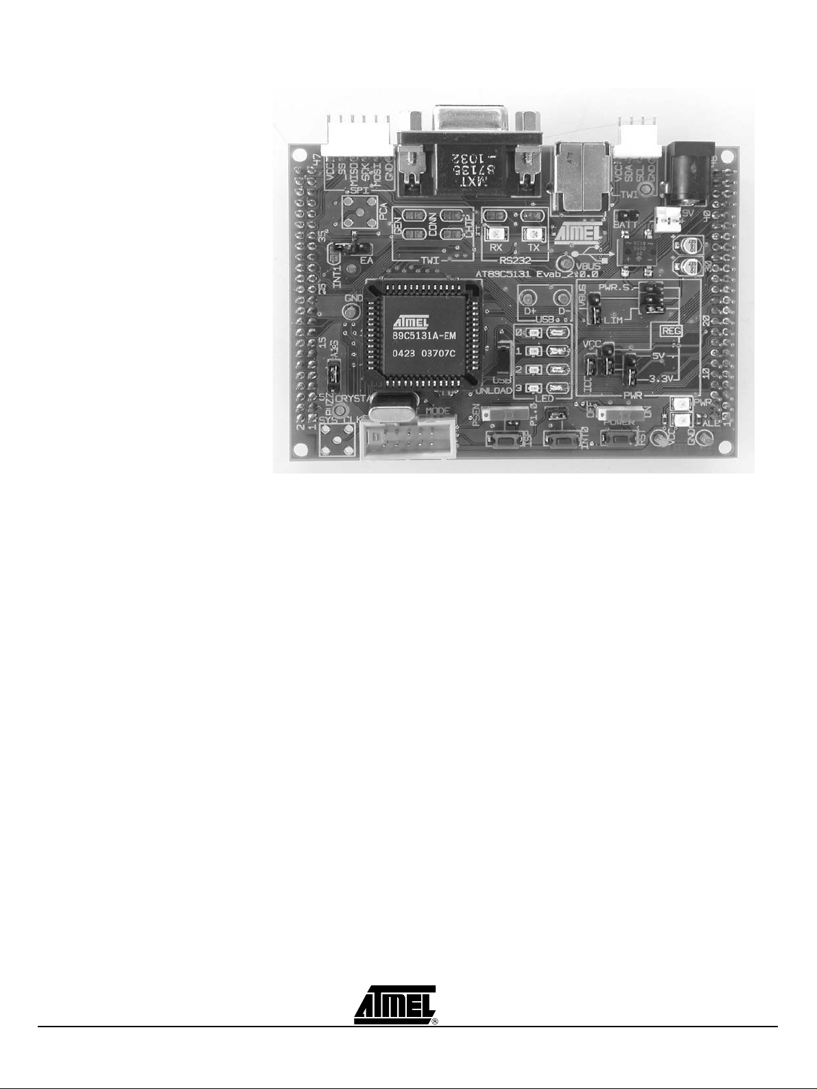
Figure 1-1. AT89C5131A Evaluation Board
1-2 AT89C5131A Starter Kit Hardware User Guide
4245A–USB–11/04
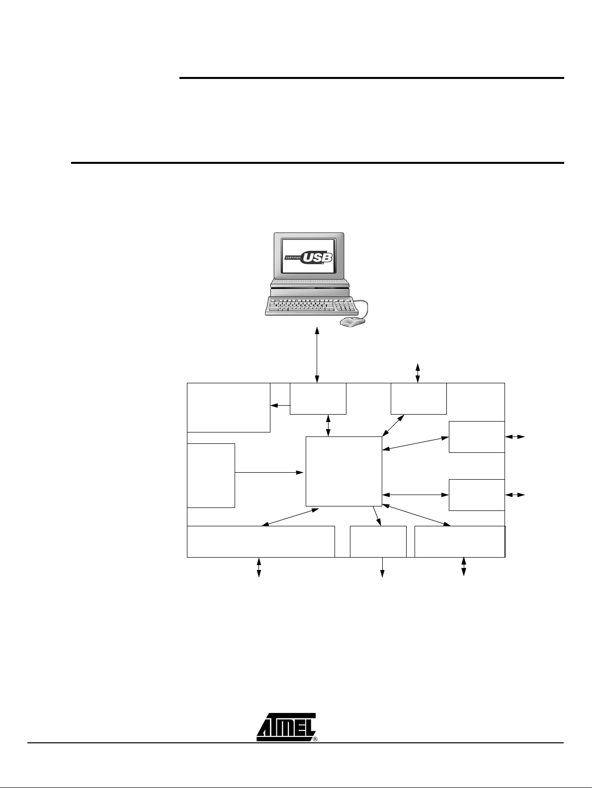
2.1 Block Diagram
...
Hardware Description
Section 2
Hardware Description
Figure 2-1. AT89C5131A Evaluation Board Components
Power
Supply
Reset
ISP
EA
INT0
C51 Generic Board Interface
C51 Generic Board
USB TWI
AT89C5131A
LED
Human
Device
SPI
RS232
Programming
Interface
Specific Device
Device
Host,
Device
AT89C5131A Starter Kit Hardware User Guide 2-3
4245A–USB–11/04
Hardware Description
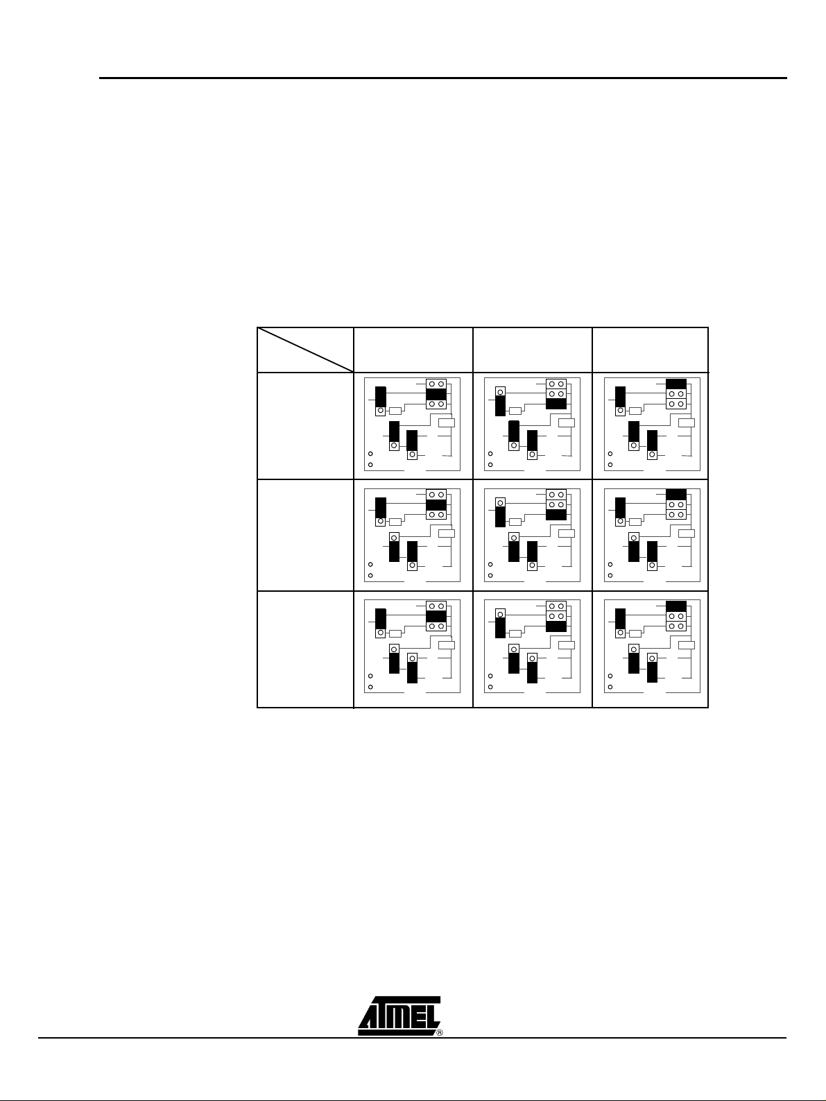
2.2 Power Supply The on-board power supply circuitry allows various power supply configurations.
The power source can be:
–V
–V
– External power supply (from 6 to 12V) or 9V battery
The voltage output can be the direct power source, regulated at 5V or 3.3V.
The power supply selection is performed using the JP2, JP3, JP4 and JP5 jumpers.
The power supply can be turned on/off using the “power” switch (SW6). Once the power
is established, the power LED (D9) is lit.
Figure 2-2. Different Power Configurations
Regulation
Direct Input
from USB (5V)
BUS
from USB (5V) through the current limiter
BUS
Power
Source
VBUS VBUS and
Current Limiter
VCC
PWR.S.
VBUS
LIM
ICC
REG
5V
3.3V
PWR
PWR.S.
VBUS
LIM
VCC
ICC
PWR
5V
3.3V
REG
VBUS
VCC
ICC
External
PWR.S.
LIM
REG
5V
3.3V
PWR
5V Regulate
3.3V Regulate
VCC
VCC
PWR.S.
VBUS
LIM
ICC
PWR.S.
VBUS
LIM
ICC
REG
5V
3.3V
PWR
REG
5V
3.3V
PWR
VCC
VCC
PWR.S.
VBUS
LIM
ICC
PWR.S.
VBUS
LIM
ICC
REG
5V
3.3V
PWR
REG
5V
3.3V
PWR
VCC
VCC
PWR.S.
VBUS
LIM
ICC
PWR.S.
VBUS
LIM
ICC
REG
5V
3.3V
PWR
REG
5V
3.3V
PWR
2-4 AT89C5131A Starter Kit Hardware User Guide
4245A–USB–11/04
Hardware Description
2.3 C51 Standard Settings
2.3.1 Reset The external Reset push-button (SW3) is provided to easily generate a warm reset. This
button is used for ISP process. The Reset applied is active low.
2.3.2 Clock A crystal can be eas ily in st all ed on the Y1 socket. The clock can als o be pr ovid ed us in g
the J8 connector instead of the crystal.
Note: Remove the clock generators before the using the programmer.
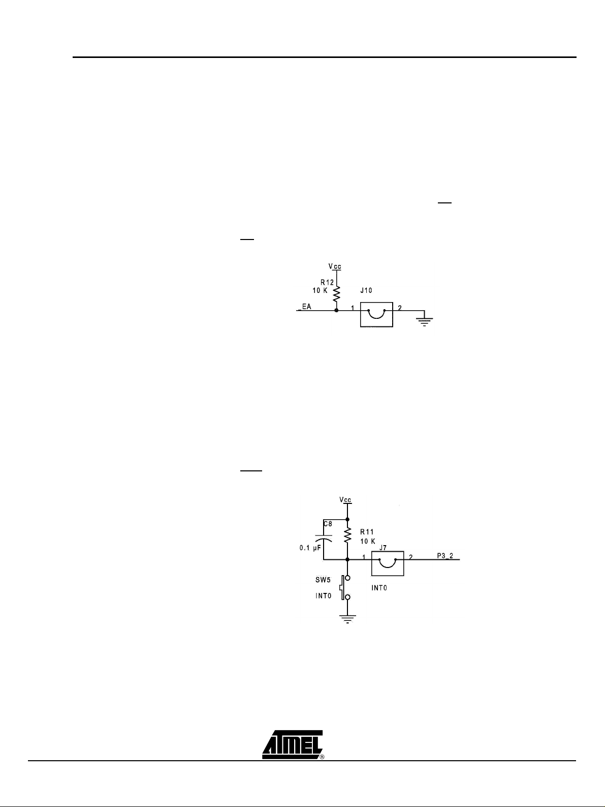
2.3.3 EA Place a jumper on the EA connector (J 10) to force the EA
pin to ground and execute
external code. Otherwise internal code will be executed. Figure 2-3. EA
Circuitry
2.3.4 INT0 In order to use the on-board INT0 circuitry, connect the J7 Jumper to the AT89C5131A.
When you press the INT0 button (SW5), the P3.2 pin will go low which induces an interrupt event.
Note: Remove the J7 jumper before using the programmer. Otherwise the program-
mer will not function.
Figure 2-4. INT0
Circuitry
AT89C5131A Starter Kit Hardware User Guide 2-5
4245A–USB–11/04
 Loading...