

Page 1

Features
®
• AVR
• USB Hub with One Attached and Two External Ports
• USB Function with Three Programmable End-points
• 24 KB Program Memory, 1 KB Data SRAM
• 32 x 8 General-purpose Working Registers
• 27 Programmable I/O Port Pins
• 12-channel 10-bit ADC
• Master/Slave SPI Serial Interface
• One 8-bit Timer/Counter with Separate Pre-scaler
• One 16-bit Timer/Counter with Separate Pre-scaler and Two PWMs
• External and Internal Interrupt Sources
• Programmable Watchdog Timer
• 6 MHz Oscillator with On-chip PLL
• 5V Operation with On-chip 3.3V Power Supply
• 64-lead LQFP Package
8-bit RISC Microcontroller with 83 ns Instruction Cycle Time
Full-speed
USB
Microcontroller
with Embedded
Description
The Atmel AT43USB355 is an 8-bit microcontroller based on the AVR RISC architecture. By executing powerful instructions in a single clock cycle, the AT43USB355
achieves throughputs approaching 12 MIPS. The AVR core combines a rich instruction set with 32 general-purpose working registers. All 32 registers are directly
connected to the ALU allowing two independent registers to be accessed in one single
instruction executed in one clock cycle. The resulting architecture is more code efficient while achieving throughputs up to ten times faster than conventional CISC
microcontrollers.
Furthermore, the AT43USB355 features an on-chip 24-Kbyte program memory and
1-Kbyte of data memory. It is supported by a standard set of peripherals such as
timer/counter modules, watchdog timer and internal and external interrupt sources.
The major peripheral included in the AT43USB355 is a full-speed USB 2.0 Hub with
an embedded function and a 12-channel Analog-to-Digital Converter (ADC) for use in
applications such as game controllers.
Hub, ADC and
PWM
AT43USB355
2603G–USB–04/06
1
Page 2
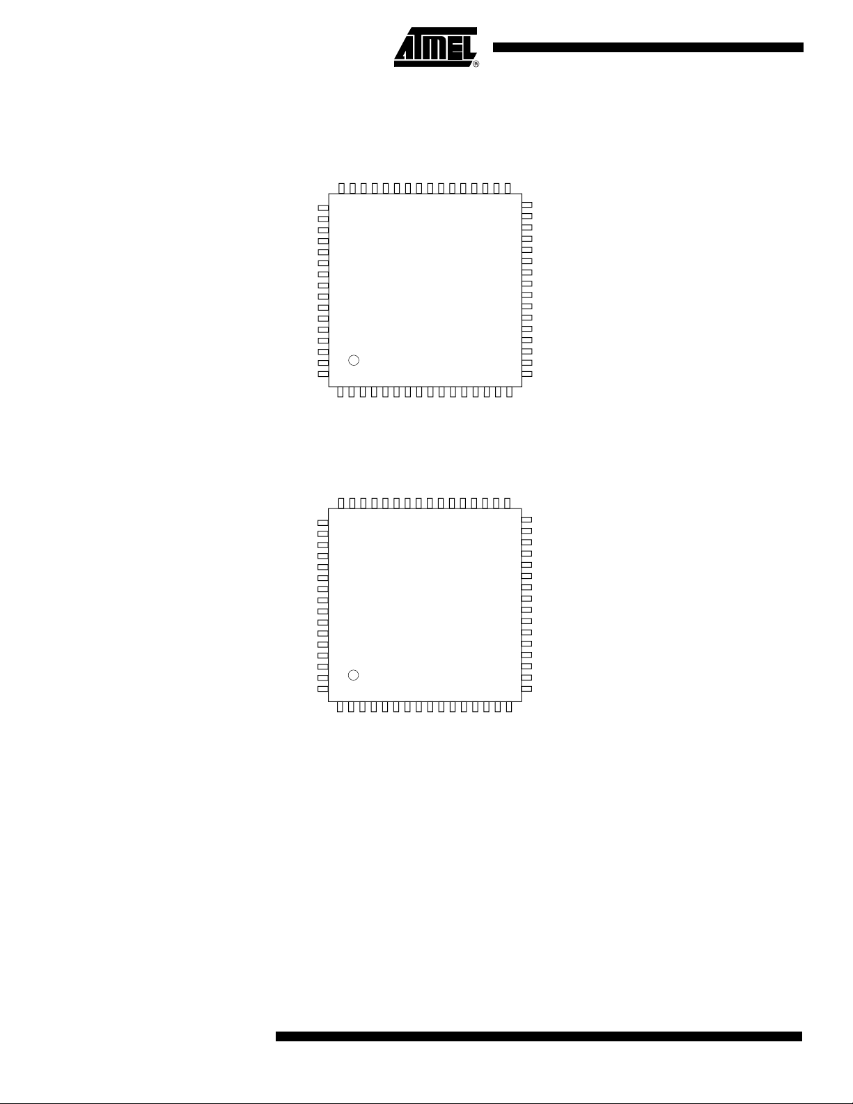
Pin Configuration
Figure 1. AT43USB355E 64-lead LQFP
Figure 2. AT43USB355M 64-lead LQFP
SCK
SSN
MOSI
MISO
CEXT3
VCC3
VSS3
PD7
PD6
PD5
XTAL1
XTAL2
PD4
PD3
PD2
PF1
PF2
PF3
CEXT3
VCC3
VSS3
PD7
PD6
PD5
XTAL1
XTAL2
PD4
PD3
PD2
VREF
VSSA
CEXTA
VCCA
ADC0
ADC1
ADC2
ADC3
ADC4
ADC5
ADC6
ADC7
ADC8
ADC9
ADC10
ADC11
33
34
35
36
37
38
39
40
41
42
43
44
45
46
47
48
49
50
51
52
53
54
55
56
57
58
59
60
61
LFT
62
63
64
1
PD1
VREF
48
49
50
NC
51
52
53
54
55
56
57
58
59
60
61
LFT
62
63
64
1
AT43USB355E-AC
2345678910111213141516
PD0
VSSA
47
DP3
CEXTA
46
DM3
VCCA
45
DP2
ADC0
44
DM2
ADC1
43
DP0
ADC2
42
DM0
ADC3
41
CEXT2
ADC4
40
VCC2
ADC5
39
VSS2
ADC6
38
PB7
ADC7
37
AT43USB355M-AC
2345678910111213141516
PB6
ADC8
36
PB5
ADC9
35
PB4
ADC10
34
32
31
30
29
28
27
26
25
24
23
22
21
20
19
18
17
PB3
ADC11
33
32
31
30
29
28
27
26
25
24
23
22
21
20
19
18
17
TEST
RESETN
PA0
PA1
PA2
PA3
CEXT1
VCC1
VSS1
PA4
PA5
PA6
PA7
PB0
PB1
PB2
TEST
RESETN
PA0
PA1
PA2
PA3
CEXT1
VCC1
VSS1
PA4
PA5
PA6
PA7
PB0
PB1
PB2
PB7
PB6
PB5
PB4
PD1
DP3
DP2
DM3
DM2
DP0
DM0
VSS2
VCC2
CEXT2
PD0
2
AT43USB355
PB3
2603G–USB–04/06
Page 3

AT43USB355
Pin Assignment
Pin# Signal Type Pin# Signal Type
1 PD1 Bi-directional 33 ADC11 Input
2 PD0 Bi-directional 34 ADC10 Input
3 DP3 Bi-directional 35 ADC9 Input
4 DM3 Bi-directional 36 ADC8 Input
5 DP2 Bi-directional 37 ADC7 Input
6 DM2 Bi-directional 38 ADC6 Input
7 DP0 Bi-directional 39 ADC5 Input
8 DM0 Bi-directional 40 ADC4 Input
9 CEXT2 Power Supply/Ground 41 ADC3 Input
10 VCC2 Power Supply/Ground 42 ADC2 Input
11 VSS2 Power Supply/Ground 43 ADC1 Input
12 PB7 Bi-directional 44 ADC0 Input
13 PB6 Bi-directional 45 VCCA Power Supply/Ground
14 PB5 Bi-directional 46 CEXTA Power Supply/Ground
15 PB4 Bi-directional 47 VSSA Power Supply/Ground
16 PB3 Bi-directional 48 VREF Input
17 PB2 Bi-directional 49 SCK/PF1 Bi-directional
18 PB1 Bi-directional 50 SSN/NC –
19 PB0 Bi-directional 51 MOSI/PF2 Bi-directional
20 PA7 Bi-directional 52 MISO/PF3 Bi-directional
21 PA6 Bi-directional 53 CEXT3 Power Supply/Ground
22 PA5 Bi-directional 54 VCC3 Power Supply/Ground
23 PA4 Bi-directional 55 VSS3 Power Supply/Ground
24 VSS1 Power Supply/Ground 56 PD7 Bi-directional
25 VCC1 Power Supply/Ground 57 PD6 Bi-directional
26 CEXT1 Power Supply/Ground 58 PD5 Bi-directional
27 PA3 Bi-directional 59 XTAL1 Input
28 PA2 Bi-directional 60 XTAL2 Output
29 PA1 Bi-directional 61 LFT Output
30 PA0 Bi-directional 62 PD4 Bi-directional
31 RESETN Input 63 PD3 Bi-directional
32 TEST Input 64 PD2 Bi-directional
2603G–USB–04/06
3
Page 4

Signal Description
Name Type Function
V
CC1, 2, 3
V
CCA
V
V
CEXT1, 2, 3 Power Supply/Ground
CEXTA Power Supply/Ground
XTAL1 Input Oscillator Input – Input to the inverting oscillator amplifier.
XTAL2 Output Oscillator Output – Output of the inverting oscillator amplifier.
LFT Input
DPO Bi-directional
DMO Bi-directional Upstream Minus USB I/O
DP[2,3] Bi-directional
DM[2,3] Bi-directional
PA[0:7] Bi-directional
Power Supply/Ground Digital Ground
SS1, 2, 3
SSA
Power Supply/Ground 5V Digital Power Supply
Power Supply/Ground 5V Power Supply for the ADC
Power Supply/Ground Ground for the ADC
External Capacitors for Power Supplies – High quality 2.2 µF capacitors must be
connected to CEXT1, 2 and 3 for proper operation of the chip.
External Capacitor for Analog Power Supply – A high quality 0.33 µF capacitor
must be connected to CEXTA for proper operation of the chip.
PLL Filter – For proper operation of the PLL, this pin should be connected through
a 0.01 µF capacitor in parallel with a 100Ω resistor in series with a 0.1 µF capacitor
to ground (VSS). Both capacitors must be high quality ceramic.
Upstream Plus USB I/O – This pin should be connected to CEXT1 through an
external 1.5 kΩ.
Downstream Plus USB I/O – Each of these pins should be connected to VSS
through an external 15 kΩ resistor. DP[2,3] and DM[2,3] are the differential signal
pin pairs to connect downstream USB devices.
Downstream Minus USB I/O – Each of these pins should be connected to VSS
through an external 15 kΩ resistor.
Port A[0:7] – Bi-directional 8-bit I/O port with 2 mA drive strength and a
programmable pull-up resistor.
PB[0:7] Bi-directional
4
AT43USB355
Port B[0:7] – Bi-directional 8-bit I/O port with 2 mA drive strength and a
programmable pull-up resistor. PB[0,1,4:7] have dual functions as shown below:
Port Pin Alternate Function
PB0 T0, Timer/Counter0 External Input
PB1 T1, Timer/Counter1 External Input
PB4 SSN, SPI Slave Port Select or SCL, I2C Serial Bus Clock
PB5 MOSI, SPI Slave Port Select Input
PB6 MISO, SPI Master Data In, Slave Data Out
PB7 SCK, SPI Master Clock Out, Slave Clock In
2603G–USB–04/06
Page 5

Signal Description (Continued)
Name Type Function
Port D[0:7] – Bi-directional I/O ports with 2 mA drive strength and a programmable
pull-up resistor. PortD[2,3,5,6] have dual functions as shown below:
Port Pin Alternate Function
AT43USB355
PD[0:7] Bi-directional
PF[1:3] Bi-directional
SSN/NC Output
ADC[0:11] Input ADC Input[0:11] – 12-bit input pins for the ADC.
AREF Input Analog Reference – Input for the ADC.
TEST Input Test Pin – This pin should be tied to ground.
RESETN Input Reset – Active Low.
PD2 INT0, External Interrupt 0
PD3 INT1, External Interrupt 1
PD5 OC1A Timer/Counter1 Output Compare A
PD6 OC1B Timer/Counter1 Output Compare B
Port F[1:3] – Bi-directional 3-bit I/O port with 2 mA drive strength and a
programmable pull-up resistor. In the AT43USB355E, PF[1:3] pins have dual
functions as the interface pins to the serial EEPROM. After program memory
downloading is complete, PF3 has a third function as Timer/Counter1 Input
Capture, ICP.
Port Pin Alternate Function
PF1 SCK, SPI Master Clock Out
PF2 MOSI, SPI Slave Data Input
PF3 MISO, SPI Slave Data Out. ICP after download complete
Slave Select – In the AT43USB355E, this pin enables the external serial memory.
In the AT43USB355M, this pin has no function and can be left floating or connected
to VCEXT.
2603G–USB–04/06
5
Page 6
Figure 3. AT43USB355 Enhanced RISC Architecture
12K x 16
Program
Memory
Instruction
Register
Instruction
Decoder
Control
Lines
Program
Counter
Status and
Control
32 x 8
General-purpose
Registers
ALU
1024 x 8
SRAM
27 GPIO
Lines
Interrupt
Unit
8-bit
Timer/Counter
16-bit
Timer/Counter
Watchdog
Timer
SPI Unit
ADC
USB
Hub and
Function
6
AT43USB355
2603G–USB–04/06
Page 7

AT43USB355
Architectural Overview
The AT43USB355 is available in 2 versions. The program memory of the AT43USB355E is an
SRAM that is automatically written from an external serial EEPROM during power-on. The
AT43USB355M has a masked ROM program memory. The two versions are pin, function and
binary compatible.
The peripherals and features of the AT43USB355 microcontroller are similar to those of the
AT90S8515, with the exception of the following modifications:
• The AT43USB355E has a downloadable SRAM and the AT43USB355M has a masked
ROM for program memory
• No EEPROM
• No external data memory accesses
•No UART
• Idle mode not supported
• USB Hub with attached function
• On-chip ADC
The embedded USB hardware of the AT43USB355 is a compound device, consisting of a 3
port hub with a permanently attached function on one port. The hub and attached function are
two independent USB devices, each having its own device addresses and control end-points.
The hub has its dedicated interrupt end-point, while the USB function has 3 additional programmable end-points with separate FIFOs. Two of the FIFOs are 64 bytes deep and the third
is 8 bytes deep.
The microcontroller always runs from a 12 MHz clock that is generated by the USB hardware.
While the nominal and average period of this clock is 83.3 ns, it may have single cycles that
deviate by ±20.8 ns during a phase adjustment by the SIE's clock/data separator of the USB
hardware.
The microcontroller shares most of the control and status registers of the megaAVR Microcontroller Family. The registers for managing the USB operations are mapped into its SRAM
space. The I/O section on page 16 summarizes the available I/O registers. The “AVR Register
Set” on page 37 covers the AVR registers. Please refer to the Atmel AVR manual for more
information.
The fast-access register file concept contains 32 x 8-bit general-purpose working registers
with a single clock cycle access time. This means that during one single clock cycle, one Arithmetic Logic Unit (ALU) operation is executed. Two operands are output from the register file,
the operation is executed, and the result is stored back in the register file – in one clock cycle.
Six of the 32 registers can be used as three 16-bit indirect address register pointers for Data
Space addressing - enabling efficient address calculations. One of the three address pointers
is also used as the address pointer for look-up tables in program memory. These added function registers are the 16-bit X-, Y- and Z-registers.
The ALU supports arithmetic and logic operations between registers or between a constant
and a register. Single register operations are also executed in the ALU. Figure 3 on page 6
shows the AT43USB355 AVR Enhanced RISC microcontroller architecture.
In addition to the register operation, the conventional memory addressing modes can be used
on the register file as well. This is enabled by the fact that the register file is assigned the 32
lowest Data Space addresses ($00 - $1 F), allowing them to be accessed as though they were
ordinary memory locations.
The I/O memory space contains 64 addresses for CPU peripheral functions as Control Registers, Timer/Counters, and other I/O functions. The I/O Memory can be accessed directly, or as
the Data Space locations following those of the register file, $20 - $5F.
2603G–USB–04/06
7
Page 8

The AVR uses a Harvard architecture concept – with separate memories and buses for program and data. The program memory is executed with a single-level pipelining. While one
instruction is being executed, the next instruction is pre-fetched from the program memory.
This concept enables instructions to be executed in every clock cycle. The program memory is
a downloadable SRAM or a mask programmed ROM.
With the relative jump and call instructions, the whole 24K address space is directly accessed.
Most AVR instructions have a single 16-bit word format. Every program memory address contains a 16- or 32-bit instruction.
During interrupts and subroutine calls, the return address Program Counter (PC) is stored on
the stack. The stack is effectively allocated in the general data SRAM, and consequently, the
stack size is only limited by the total SRAM size and the usage of the SRAM. All user programs must initialize the Stack Pointer (SP) in the reset routine (before subroutines or
interrupts are executed). The 10-bit SP is read/write accessible in the I/O space.
The 1-Kbyte data SRAM can be easily accessed through the five different addressing modes
supported in the AVR architecture.
The memory spaces in the AVR architecture are all linear and regular memory maps. A flexible interrupt module has its control registers in the I/O space with an additional global interrupt
enable bit in the status register. All interrupts have a separate interrupt vector in the interrupt
vector table at the beginning of the program memory. The interrupts have priority in accordance with their interrupt vector position. The lower the interrupt vector address, the higher the
priority.
The Generalpurpose
Register File
Table 1. AVR CPU General-purpose Working Register
Register Address Comment
R0 $00
R1 $01
R2 $02
..
R13 $0D
R14 $0E
R15 $0F
R16 $10
R17 $11
..
R26 $1A X-register low byte
R27 $1B X-register high byte
R28 $1C Y-register low byte
R29 $1D Y-register high byte
R30 $1E Z-register low byte
R31 $1F Z-register high byte
8
AT43USB355
2603G–USB–04/06
Page 9

AT43USB355
All register operating instructions in the instruction set have direct and single cycle access to
all registers. The only exception is the five constant arithmetic and logic instructions SBCI,
SUBI, CPI, ANDI, and ORI between a constant and a register, and the LDI instruction for load
immediate constant data. These instructions apply to the second half of the registers in the
register file – R16..R31. The general SBC, SUB, CP, AND, and OR and all other operations
between two registers or on a single register apply to the entire register file.
As shown in Table 1, each register is also assigned a data memory address, mapping them
directly into the first 32 locations of the user Data Space. Although not being physically implemented as SRAM locations, this memory organization provides great flexibility in access of the
registers, as the X-, Y-, and Z-registers can be set to index any register in the file.
X-, Y- and ZRegisters
Registers R26..R31 contain some added functions to their general-purpose usage. These registers are address pointers for indirect addressing of the Data Space. The three indirect
address registers X, Y, and Z are defined as:
X-register 15 XH XL 0
7070
R27 ($1B) R26 ($1A)
Y-register 15 YH YL 0
7070
R29 ($1D) R28 ($1C)
Z-register 15 ZH ZL 0
7070
R30 ($1F) R31 ($1E)
In the different addressing modes these address registers have functions as fixed displacement, automatic increment and decrement (see the descriptions for the different instructions).
ALU – Arithmetic
Logic Unit
The high-performance AVR ALU operates in direct connection with all 32 general-purpose
working registers. Within a single clock cycle, ALU operations between registers in the register
file are executed. The ALU operations are divided into three main categories – arithmetic, logical and bit-functions.
Program Memory The AT43USB355E contains 24K bytes on-chip downloadable memory for program storage
while the AT43USB355M has a masked programmable ROM. Since all instructions are 16- or
32-bit words, the program memory is organized as 12K x 16. The AT43USB355 Program
Counter (PC) is 14 bits wide, thus addressing the 12,288 program memory addresses.
Constant tables can be allocated within the entire program memory address space (see the
LPM - Load Program Memory instruction description).
2603G–USB–04/06
9
Page 10
The program memory of the AT43USB355E is automatically written with data stored in an
external serial EEPROM during the chip's power-on reset sequence. The power-on reset is
the only way the on-chip program memory of the AT43USB355E will be written or modified.
The two versions of the AT43USB355 are binary compatible. A firmware written for the
AT43USB355E will work unaltered on the AT43USB355M. The only functional difference
between the two versions is with respect to the serial EEPROM interface pins, GPIO PF[0:3].
The differences are:
Port F Pins AT43USB355E AT43USB355M
PF0 Slave Select Pin – Its output will be asserted (low) during
downloading of firmware and will stay de-asserted (high) after
download is completed.
PF1, PF2, PF3 Functions as serial EEPROM interface signals during
downloading and as GPIO pins after download is completed.
NC (No connect)
GPIO
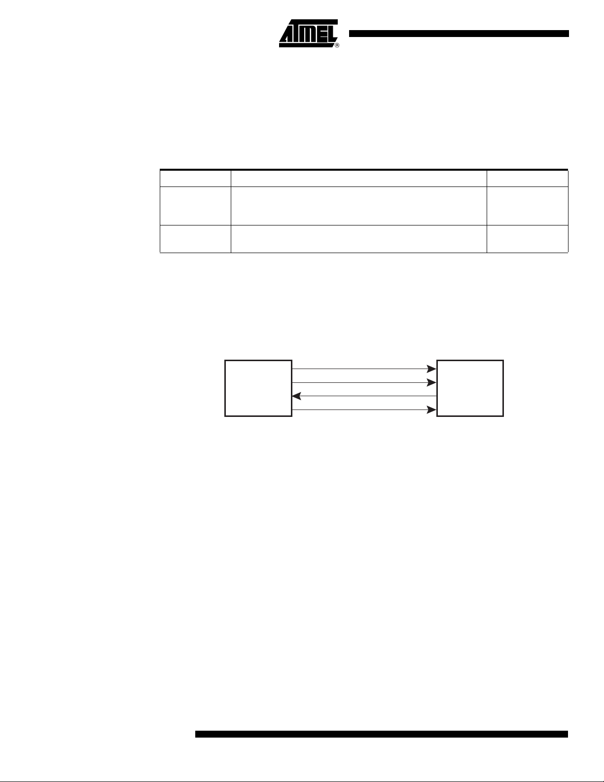
SPI Serial EEPROM Interface (AT43USB355E Only)
The AT43USB355E is designed to interface directly with a synchronous serial peripheral interface (SPI) SEEPROM such as the Atmel AT25HP256/512. All instructions, addresses and
data are transferred with the MSB first and start with a high-to-low SSN transition.
Note: The SPI port of the AT43USB355E at PF[0:3] is dedicated for program memory downloading
only. It cannot be accessed by the firmware program.
Figure 4. AT43USB355E Read Sequence
SSN
AT43USB355E AT25HP256
MOSI
MISO
SCK
Read Sequence 1. The AT43USB35E asserts its SSN output pin and outputs a 3 MHz clock at SCK. It
continues to activate SCK until the completion of the read process.
2. The AT43USB355E transmits the READ op-code (= 0000011) through its MOSI, followed by the 16-bit byte address to be read, x0000. Please note that the
AT43USB355E will send a 16-byte address only. SEEPROM with SPI that requires a
24-bit address cannot be used with the AT43USB355E.
3. The SEEPROM then shifts out the data through its MISO pin.
4. The AT43USB35E de-asserts SCK and SSN after 24K bytes data read is complete.
10
AT43USB355
2603G–USB–04/06
Page 11
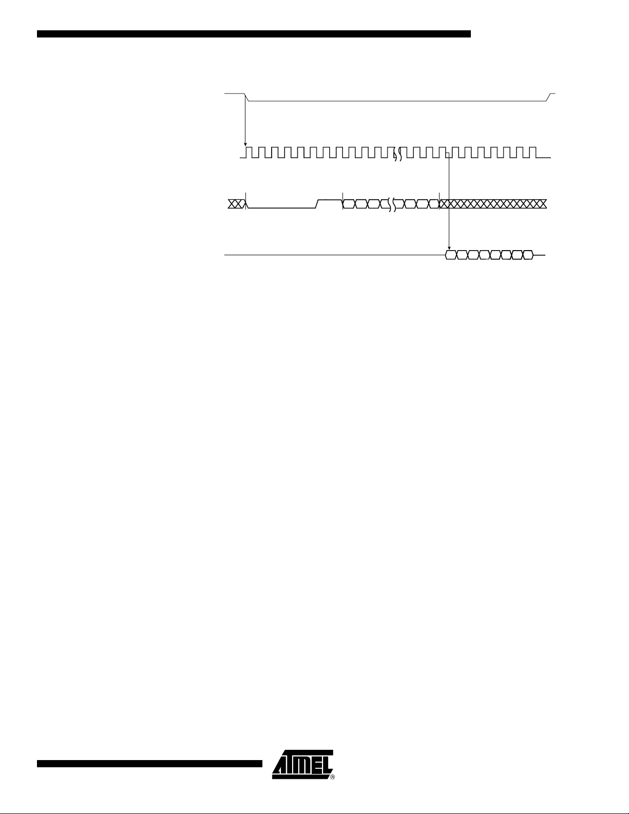
Figure 5. READ Timing
SSN
AT43USB355
SRAM Data Memory
SCK
MOSI
MISO
1 2 3 4 5 6 7 8 9 101120212223242526272829300
INSTRUCTION
HIGH IMPEDANCE
BYTE ADDRESS
...
0123131415
DATA OUT
2 0134567
MSB
Table 3 summarizes how the AT43USB355 SRAM Memory is organized. The lower 1120 Data
Memory locations address the Register file, the I/O Memory and the internal data SRAM. The
first 96 locations address the Register File + I/O Memory, and the next 1024 locations address
the internal data SRAM. The five different addressing modes for the data memory cover:
Direct, Indirect with Displacement, Indirect, Indirect with Pre-decrement and Indirect with Postincrement. In the register file, registers R26 to R31 feature the indirect addressing pointer registers. Direct addressing reaches the entire data space.
The Indirect with Displacement mode features 63 address locations that reach from the base
address given by the Y- or Z-register.
When using register indirect addressing modes with automatic pre-decrement and post-increment, the address registers X, Y, and Z are decremented and incremented.
The 32 general-purpose working registers, 64 I/O registers and the 1024 bytes of internal data
SRAM in the AT43USB355 are all accessible through these addressing modes.
To manage the USB hardware, a special set of registers is assigned. These registers are
mapped to SRAM space between addresses $1F00 and 1FFF. Table 3 and Table 4 give an
overview of these registers.
2603G–USB–04/06
11
Page 12

Table 2. SRAM Organization
Register File Data Address Space
R0 $0000
R1 $0001
R30 $001E
R31 $001F
I/O Registers
$00 $0020
$01 $0021
$3E $005E
$3F $005F
Internal SRAM
$0060
$0061
$025E
$045F
USB Registers
$1F00
$1FFE
$1FFF
12
AT43USB355
2603G–USB–04/06
Page 13

AT43USB355
Table 3. USB Hub and Function Registers
Address Name Function
$1FFD FRM_NUM_H Frame Number High Register
$1FFC FRM_NUM_L Frame Number Low Register
$1FFB GLB_STATE Global State Register
$1FFA SPRSR Suspend/Resume Register
$1FF9 SPRSIE Suspend/Resume Interrupt Enable Register
$1FF8 SPRSMSK Suspend/Resume Interrupt Mask Register
$1FF7 UISR USB Interrupt Status Register
$1FF6 UIMSKR USB Interrupt Mask Register
$1FF5 UIAR USB Interrupt Acknowledge Register
$1FF3 UIER USB Interrupt Enable Register
$1FF2 UOVCER Overcurrent Detect Register
$1FEF HADDR Hub Address Register
$1FEE FADDR Function Address Register
$1FE7 HEND-P0_CNTR Hub End-point 0 Control Register
$1FE5 FEND-P0_CNTR Function End-point 0 Control Register
$1FE4 FEND-P1_CNTR Function End-point 1 Control Register
$1FE3 FEND-P2_CNTR Function End-point 2 Control Register
$1FE2 FEND-P3_CNTR Function End-point 3 Control Register
$1FDF HCSR0 Hub Controller End-point 0 Service Routine Register
$1FDD FCSR0 Function Controller End-point 0 Service Routine Register
$1FDC FCSR1 Function Controller End-point 1 Service Routine Register
$1FDB FCSR2 Function Controller End-point 2 Service Routine Register
$1FDA FCSR3 Function Controller End-point 3 Service Routine Register
$1FD7 HDR0 Hub End-point 0 FIFO Data Register
$1FD5 FDR0 Function End-point 0 FIFO Data Register
$1FD4 FDR1 Function End-point 1 FIFO Data Register
$1FD3 FDR2 Function End-point 2 FIFO Data Register
$1FD2 FDR3 Function End-point 3 FIFO Data Register
$1FCF HBYTE_CNT0 Hub End-point 0 Byte Count Register
$1FCD FBYTE_CNT0 Function End-point 0 Byte Count Register
$1FCC FBYTE_CNT1 Function End-point 1 Byte Count Register
$1FCB FBYTE_CNT2 Function End-point 2 Byte Count Register
$1FCA FBYTE_CNT3 Function End-point 3 Byte Count Register
$1FC7 HSTR Hub Status Register
2603G–USB–04/06
$1FC5 HPCON Hub Port Control Register
13
Page 14

Table 3. USB Hub and Function Registers (Continued)
Address Name Function
$1FBA HPSTAT3 Hub Port 3 Status Register
$1FB9 HPSTAT2 Hub Port 2 Status Register
$1FB8 HPSTAT1 Hub Port 1 Status Register
$1FB2 HPSCR3 Hub Port 3 Status Change Register
$1FB1 HPSCR2 Hub Port 2 Status Change Register
$1FB0 HPSCR1 Hub Port 1 Status Change Register
$1FAA PSTATE3 Hub Port 3 Bus State Register
$1FA9 PSTATE2 Hub Port 2 Bus State Register
$1FA7 HCAR0 Hub End-point 0 Control and Acknowledge Register
$1FA5 FCAR0 Function End-point 0 Control and Acknowledge Register
$1FA4 FCAR1 Function End-point 1 Control and Acknowledge Register
$1FA3 FCAR2 Function End-point 2 Control and Acknowledge Register
$1FA2 FCAR3 Function End-point 3 Control and Acknowledge Register
14
AT43USB355
2603G–USB–04/06
Page 15

AT43USB355
Table 4. USB Hub and Function Registers
Name Address Bit 7 Bit 6 Bit 5 Bit 4 Bit 3 Bit 2 Bit 1 Bit 0
GLB_STATE $1FFB – SUSP FLG RESUME FLG RMWUPE CONFG HADD EN
SPRSR $1FFA – – – – – FRWUP RSM GLB SUSP
SPRSIE $1FF9 – – – – – FRWUP IE RSM IE GLB SUSP IE
SPRSMSK $1FF8 – – – – – FRWUP MSK RSM MSK GLB SUSP MSK
UISR $1FF7 SOF INT EOF2 INT – FEP3 INT HEP0 INT FEP2 INT FEP1 INT FEP0 INT
UIMSKR $1FF6 SOF MSK SOF2 MSK – FEP3 MSK HEP0 MSK FEP2 MSK FEP1 MSK FEP0 MSK
UIAR $1FF5 SOF INTACK EOF2 INTACK – FEP3 INTACK HEP0 INTACK FEP2 INTACK FEP1 INTACK FEP0 INTACK
UIER $1FF3 SOF IE EOF2 IE – FEP3 IE HEP0 IE FEP2 IE FEP1 IE FEP0 IE
UOVCER $1FF2 – – – – OVC3 OVC2 – –
HADDR $1FEF SAEN HADD6 HADD5 HADD4 HADD3 HADD2 HADD1 HADD0
FADDR $1FEE FEN FADD6 FADD5 FADD4 FADD3 FADD2 FADD1 FADD0
HEND-P0_CNTR $1FE7 EPEN – – – DTGLE EPDIR EPTYPE1 EPTYPE0
FEND-P0_CNTR $1FE5 EPEN – – – DTGLE EPDIR EPTYPE1 EPTYPE0
FEND-P1_CNTR $1FE4 EPEN – – – DTGLE EPDIR EPTYPE1 EPTYPE0
FEND-P2_CNTR $1FE3 EPEN – – – DTGLE EPDIR EPTYPE1 EPTYPE0
FEND-P3_CNTR $1FE2 EPEN – – – DTGLE EPDIR EPTYPE1 EPTYPE0
HCSR0 $1FDF – – – – STALL SENT RX SETUP RX OUT PACKET TX CEMPLETE
FCSR0 $1FDD – – – – STALL SENT RX SETUP RX OUT PACKET TX COMPLETE
FCSR1 $1FDC – – – – STALL SENT – RX OUT PACKET TX COMPLETE
FCSR2 $1FDB – – – – STALL SENT – RX OUT PACKET TX COMPLETE
FCSR3 $1FDA – – – – STALL SENT – RX OUT PACKET TX COMPLETE
HDR0 $1FD7 DATA7 DATA6 DATA5 DATA4 DATA3 DATA2 DATA1 DATA0
F DR 0 $1 F D5 DATA 7 DATA 6 D ATA5 DATA 4 DATA 3 D ATA2 DATA 1 D ATA 0
F DR 1 $1 F D4 DATA 7 DATA 6 D ATA5 DATA 4 DATA 3 D ATA2 DATA 1 D ATA 0
F DR 2 $1 F D3 DATA 7 DATA 6 D ATA5 DATA 4 DATA 3 D ATA2 DATA 1 D ATA 0
F DR 3 $1 F D2 DATA 7 DATA 6 D ATA5 DATA 4 DATA 3 D ATA2 DATA 1 D ATA 0
HBYTE_CNT0 $1FCF – – BYTCT5 BYTCT4 BYTCT3 BYTCT2 BYTCT1 BYTCT0
FBYTE_CNT0 $1FCD – – BYTCT5 BYTCT4 BYTCT3 BYTCT2 BYTCT1 BYTCT0
FBYTE_CNT1 $1FCC – BYTCT6 BYTCT5 BYTCT4 BYTCT3 BYTCT2 BYTCT1 BYTCT0
FBYTE_CNT2 $1FCB – BYTCT6 BYTCT5 BYTCT4 BYTCT3 BYTCT2 BYTCT1 BYTCT0
FBYTE_CNT3 $1FCA – – BYTCT5 BYTCT4 BYTCT3 BYTCT2 BYTCT1 BYTCT0
HSTR $1FC7 – – – – OVLSC LPSC OVI LPS
HPCON $1FC5 – HPCON2 HPCON1 HPCON0 – HPADD2 HPADD1 HPADD0
HPSTAT3 $1FBA – LSP PPSTAT PRSTAT POCI PSSTAT PESTAT PCSTAT
HPSTAT2 $1FB9 – LSP PPSTAT PRSTAT POCI PSSTAT PESTAT PCSTAT
HPSTAT1 $1FB8 – LSP PPSTAT PRSTAT POCI PSSTAT PESTAT PCSTAT
HPSCR3 $1FB2 – – – RSTSC POCIC PSSC PESC PCSC
HPSCR2 $1FB1 – – – RSTSC POCIC PSSC PESC PCSC
HPSCR1 $1FB0 – – – RSTSC POCIC PSSC PESC PCSC
PSTATE3 $1FAA – – – – – – DPSTATE DMSTATE
PSTATE2 $1FA9 – – – – – – DPSTATE DMSTATE
HCAR0 $1FA7 CTL DIR DATA END FORCE STALL TX PACKET READY STALL_SENT-ACK RX_SETUP_ACK RX_OUT_PACKET_ACK
FCAR0 $1FA5 CTL DIR DATA END FORCE STALL TX PACKET READY STALL_SENT-ACK RX_SETUP_ACK RX_OUT_PACKET_ACK
FCAR1 $1FA4 CTL DIR DATA END FORCE STALL TX PACKET READY STALL_SENT-ACK – RX_OUT_PACKET_ACK
FCAR2 $1FA3 CTL DIR DATA END FORCE STALL TX PACKET READY STALL_SENT-ACK – RX_OUT_PACKET_ACK
FCAR3 $1FA2 CTL DIR DATA END FORCE STALL TX PACKET READY STALL_SENT-ACK – RX_OUT_PACKET_ACK
TX_COMPLETEACK
TX_COMPLETEACK
TX_COMPLETEACK
TX_COMPLETEACK
TX_COMPLETEACK
2603G–USB–04/06
15
Page 16

I/O Memory The I/O space definition of the AT43USB355 is shown in the following table:
Table 5. I/O Memory Space
I/O (SRAM)
Address Name Function
$3F ($5F) SREG Status Register
$3E ($5E) SPH Stack Pointer High
$3D ($5D) SPL Stack Pointer Low
$3B ($5B) GIMSK General Interrupt Mask Register
$3A ($5A) GIFR General Interrupt Flag Register
$39 ($59) TIMSK Timer/Counter Interrupt Mask Register
$38 ($58) TIFR Timer/Counter Interrupt Flag Register
$35 ($55) MCUCR MCU General Control Register
$33 ($53) TCCR0 Timer/Counter0 Control Register
$32 ($52) TCNT0 Timer/Counter0 (8 bit)
$2F ($4F) TCCR1A Timer/Counter1 Control Register A
$2E ($4E) TTCR1B Timer/Counter1 Control Register B
$2D ($52) TCNT1H Timer/Counter1 High Byte
$2C ($52) TCNT1L Timer/Counter1 Low Byte
$2B ($4B) OCR1AH Timer/Counter1 Output Compare Register A High Byte
$2A ($4A) OCR1AL Timer/Counter1 Output Compare Register A Low Byte
$29 ($49) OCR1BH Timer/Counter1 Output Compare Register B High Byte
$28 ($48) OCR1BL Timer/Counter1 Output Compare Register B Low Byte
$25 ($45) ICR1H T/C 1 Input Capture Register High Byte
$24 ($44) ICR1L T/C 1 Input Capture Register Low Byte
$21 ($41) WDTCR Watchdog Timer Counter Register
$1B ($4B) PORTA Data Register, Port A
$1A ($3A) DDRA Data Direction Register, Port A
$19 ($39) PINA Input Pins, Port A
$18 ($38) PORTB Data Register, Port B
$17 ($37) DDRB Data Direction Register, Port B
$16 ($36) PINB Input Pins, Port B
$12 ($32) PORTD Data Register, Port D
$11 ($31) DDRD Data Direction Register, Port D
$10 ($30) PIND Input Pins, Port D
$0F ($2F) SPDR SPI I/O Data Register
$0E ($2E) SPSR SPI Status Register
$0D ($2D) SPCR SPI Control Register
16
$08 ($28) ADMUX ADC Mux Select Register
AT43USB355
2603G–USB–04/06
Page 17

AT43USB355
Table 5. I/O Memory Space (Continued)
I/O (SRAM)
Address Name Function
$07 ($27) ADCSR ADC Control and Status Register
$06 ($26) PORTF Data Register, Port F
$05 ($25) DDRF Data Direction Register, Port F
$04 ($24) PINF Input Pins, Port F
$03 ($23) ADCH ADC High Byte Data Register
$02 ($22) ADCL ADC Low Byte Data Register
All AT43USB355 I/O and peripherals, except for the USB hardware registers, are placed in the
I/O space. The I/O locations are accessed by the IN and OUT instructions transferring data
between the 32 general-purpose working registers and the I/O space. I/O registers within the
address range $00 – $1F are directly bit-accessible using the SBI and CBI instructions. In
these registers, the value of single bits can be checked by using the SBIS and SBIC instructions. Refer to the instruction set documentations of the AVR for more details. When using the
I/O specific commands, IN and OUT, the I/O address $00 – $3F must be used. When addressing I/O registers as SRAM, $20 must be added to this address. All I/O register addresses
throughout this document are shown with the SRAM address in parentheses.
For compatibility with future devices, reserved bits should be written to zero if accessed.
Reserved I/O memory addresses should never be written.
USB Hub A block diagram of the USB hardware of the AT43USB355 is shown in Figure 6. The USB hub
of the AT43USB355 has 3 downstream ports. The embedded function is permanently
attached to Port 1. Ports 2 and 3 are available as external ports. The actual number of ports
used is strictly defined by the firmware of the AT43USB355 and can vary from 0 to 2. Because
the exact configuration is defined by firmware, ports 2 and 3 may even function as permanently attached ports as long as the Hub Descriptor identifies them as such.
USB Function The embedded USB function has its own device address and has a default end-point plus 3
other programmable end-points. Two of these end-points contain their own 64-byte FIFO while
the third end-point has an 8-byte FIFO. End-points 1 - 3 can be programmed as interrupt IN or
OUT or bulk IN or OUT end-points.
2603G–USB–04/06
17
Page 18
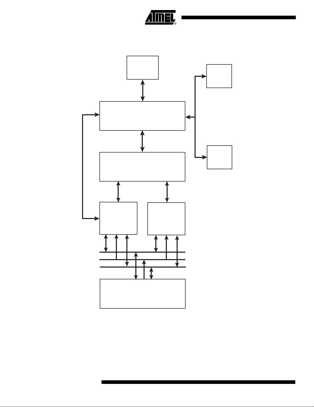
Figure 6. USB Hardware
Port 0
XCVR
Hub Repeater
Serial Interface Engine
Port 2
XCVR
Port 3
XCVR
Hub
Interface
Unit
Port 1
Function
Interface
Unit
Data
Address
Control
AVR Microcontroller
18
AT43USB355
2603G–USB–04/06
Page 19

Functional Description
AT43USB355
On-chip Power Supply
I/O Pin Characteristics
The AT43USB355 contains four on-chip power supplies that generate 3.3V with a capacity of
30 mA each from the 5V power input. The on-chip power supplies are intended to supply the
AT43USB355 internal circuit and the 1.5K pull-up resistor only and should not be used for
other purposes. External 2.2 µF filter capacitors are required at the power supply outputs,
CEXT1, 2, 3, and a 0.33 µF capacitor for CEXTA. The internal power supplies can be disabled
as described in the next paragraph.
The user should be careful when the GPIO pins are required to supply high-load currents. If
the application requires that the GPIO supply currents beyond the capability of the on-chip
power supply, the AT43USB355 should be supplied by an external 3.3V power supply. In this
case, the 5V V
the chip through the CEXT1, 2, 3 and CEXTA pins.
The I/O pins of the AT43USB355 should not be directly connected to voltages less than VSS or
more than the voltage at the CEXT pins. If it is necessary to violate this rule, insert a series
resistor between the I/O pin and the source of the external signal source that limits the current
into the I/O pin to less than 2 mA. Under no circumstance should the external voltage exceed
5.5V. To do so will put the chip under excessive stress.
power supply pin should be left unconnected and the 3.3V power supplied to
CC
Oscillator and PLL All clock signals required to operate the AT43USB355 are derived from an on-chip oscillator.
To reduce EMI and power dissipation, the oscillator is designed to operate with a 6 MHz crystal. An on-chip PLL generates the high frequency for the clock/data separator of the Serial
Interface Engine. In the suspended state, the oscillator circuitry is turned off.
The oscillator of the AT43USB355 is a special, low-drive type, designed to work with most
crystals without any external components. The crystal must be of the parallel resonance type
requiring a load capacitance of about 10 pF. If the crystal requires a higher value capacitance,
external capacitors can be added to the two terminals of the crystal and ground to meet the
required value. To assure quick start-up, a crystal with a high Q, or low ESR, should be used.
To meet the USB hub frequency accuracy and stability requirements for hubs, the crystal
should have an accuracy and stability of better than 100 PPM. The use of a ceramic resonator
in place of the crystal is not recommended because a resonator would not have the necessary
frequency accuracy and stability.
2603G–USB–04/06
The clock can also be externally sourced. In this case, connect the clock source to the XTAL1
pin, while leaving XTAL2 pin floating. The switching level at the OSC1 pin can be as low as
0.47V and a CMOS device is required to drive this pin to maintain good noise margins at the
low switching level.
For proper operation of the PLL, an external RC filter consisting of a series RC network of
100Ω and 0.1 µF in parallel with a 0.01 µF capacitor must be connected from the LFT pin to
V
. Use only high-quality ceramic capacitors.
SS
19
Page 20
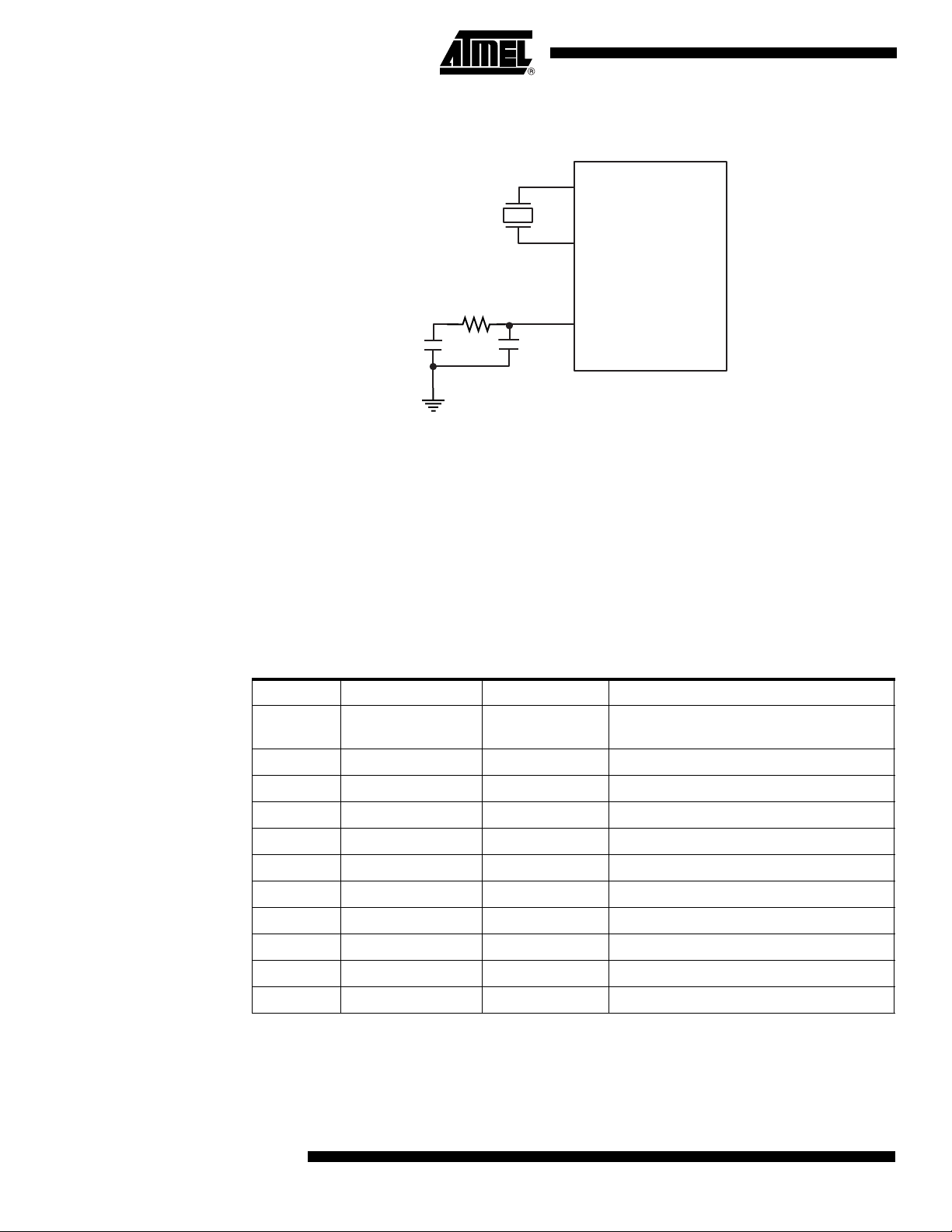
Figure 7. Oscillator and PLL
U1
Reset and Interrupt Handling
Y1
6.000 MHz
R1
100
C1
0.1 UF
0.01 UF
XTAL1
XTAL2
AT43USB355
LFT
C2
The AT43USB355 provides 20 different interrupt sources with 11 separate reset vectors, each
with a separate program vector in the program memory space. Eleven of the interrupt sources
share 2 interrupt reset vectors. These 11 are the USB related interrupts. All interrupts are
assigned individual enable bits which must be set (one) together with the I-bit in the status register in order to enable the interrupt.
The lowest addresses in the program memory space are automatically defined as the Reset
and Interrupt vectors. The complete list of vectors is shown in Table 6. The list also determines
the priority levels of the different interrupts. The lower the address, the higher is the priority
level. RESET has the highest priority, and next is INT0 – the USB Suspend and Resume Interrupt, etc.
Table 6. Reset and Interrupt Vectors
Vector No. Program Address Source Interrupt Definition
1 $000 RESET External Reset, Power-on Reset and
Watchdog Reset
2 $002 INT0 USB Suspend and Resume
3 $004 INT1 External Interrupt Request 1
4 $006 TIMER1 CAPT Timer/Counter1 Capture Event
5 $008 TIMER1 COMPA Timer/Counter1 Compare Match A
6 $00A TIMER1 COMPB Timer/Counter1 Compare Match B
7 $00C TIMER1, OVF Timer/Counter1 Overflow
8 $00E TIMER0, OVF Timer/Counter0 Overflow
9 $010 SPI, STC SPI Serial Transfer Complete
12 $016 ADC ADC Conversion Complete
13 $018 USB HW USB Hardware
20
AT43USB355
2603G–USB–04/06
Page 21

AT43USB355
The most typical and general program setup for the Reset and Interrupt Vector Addresses are:
Address Labels Code Comments
$000 jmp RESET ; Reset Handler
$004 jmp EXT_INT1 ; IRQ1 Handler
$00E jmp TIM0_OVF ; Timer0 Overflow
Handler
$018 jmp USB_HW ; USB Handler
;
$00d MAIN: ldi r16, high (RAMEND) ; Main Program
start
$00e out SPH, r16
$00f ldi r16, low (RAMEND)
$010 out SPL, r16
$011 <instr> xxx
... ... ... ...
USB related interrupt events are routed to reset vectors 13 and 2 through a separate set of
interrupt, interrupt enable and interrupt mask registers that are mapped to the data SRAM
space. These interrupts must be enabled though their control register bits. In the event an
interrupt is generated, the source of the interrupt is identified by reading the interrupt registers.
The USB frame and transaction related interrupt events, such as Start of Frame interrupt, are
grouped in one set of registers: USB Interrupt Flag Register, USB Interrupt Enable Register
and USB Interrupt Mask Register. The USB Bus reset and suspend/resume are grouped in
another set of registers: Suspend/Resume Register, Suspend/Resume Interrupt Enable Register and Suspend/Resume Interrupt Mask Register.
Some applications may include firmware routines lasting for long periods of time that cannot
be interrupted. At the same time, other less critical events may need attention after the critical
routine is completed. The AT43USB355 solves this problem by having interrupt mask registers
in addition to the interrupt enable registers of the USB related interrupts. The difference
between the mask and the enable registers is:
• The enable register enables the interrupt so it is captured into the interrupt register. If it is
not enabled and an interrupt occurs, the interrupt will be lost,
• The mask register merely masks the interrupt from interrupting the CPU. Upon
unmasking, the pending interrupt is triggered.
2603G–USB–04/06
21
Page 22
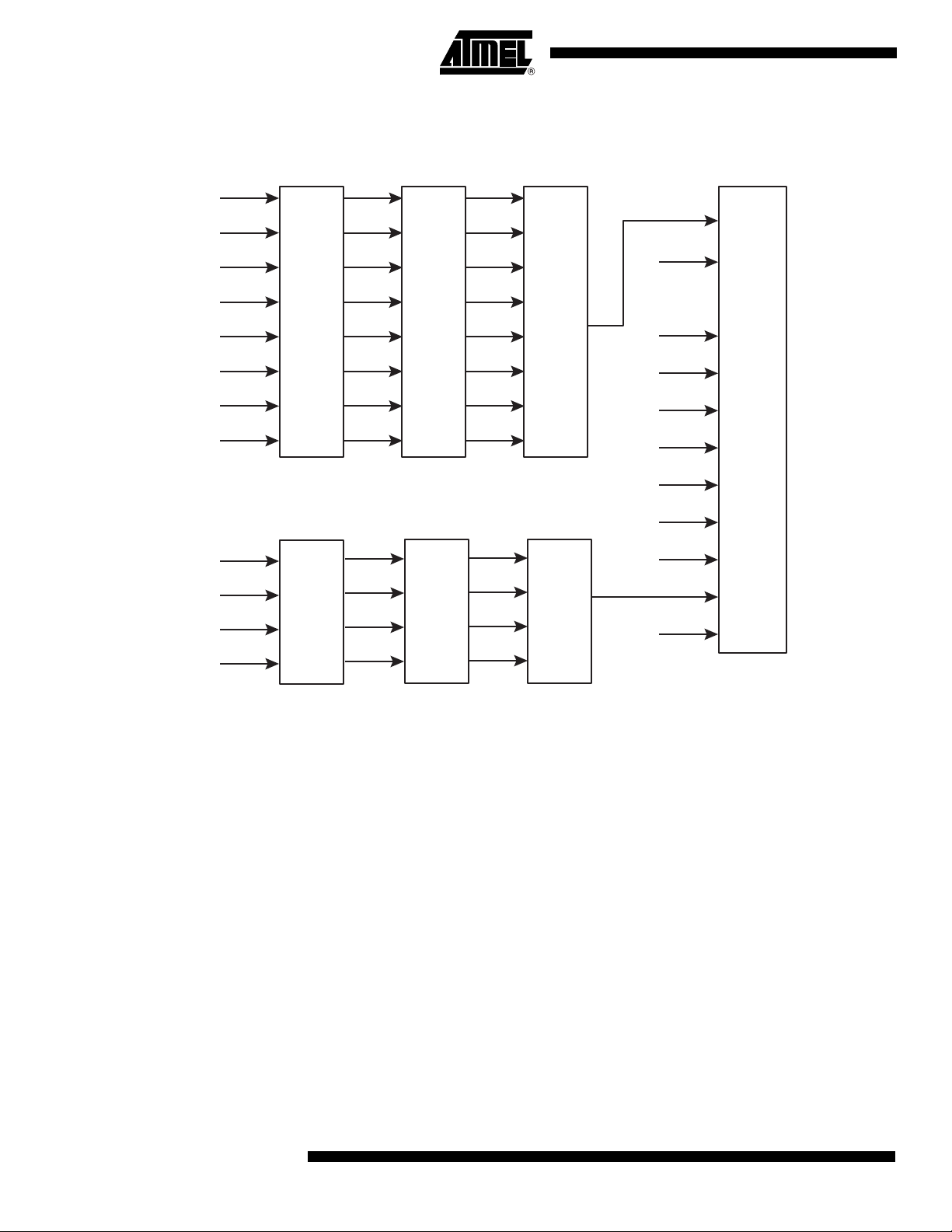
Figure 8. AT43USB355 Interrupt Structure
USB Interrupt
Flag Register
SOF
EOF2
FEP3
FEP2
USB Interrupt
Enable Register
USB Interrupt
Mask Register
USB
ADC
Microcontroller
Interrupt
Logic
13
12
FEP1
FEP0
RESERVED
HEP0
FRMWUP
RSM
GLB SUSP
BUS RESET
Suspend/Resume
Register
Suspend/Resume
Interrupt Enable
Register
Suspend/Resume
Interrupt Mask
Register
Reset Sources The AT43USB355 has four sources of reset:
• Power-on Reset – The MCU is reset when the supply voltage is below the power-on reset
threshold.
• External Reset – The MCU is reset when a low level is present on the RESETN pin for
more than 50 ns.
• Watchdog Reset – The MCU is reset when the watchdog timer period expires and the
watchdog is enabled.
• USB Reset – The AT43USB355 has a feature to separate the USB and microcontroller
resets. This feature is enabled by setting the BUS INT EN, bit 3 of the SPRSIE register. A
USB bus reset is defined as a SE0 (single ended zero) of at least 4 slow speed USB clock
cycles received by Port0. The internal reset pulse to the USB hardware and
microcontroller lasts for 24 oscillator periods.
– Resets not separated: A USB bus reset will also reset the microcontroller.
– Separated reset: A USB bus reset will only reset the USB hardware, while an
interrupt to the microcontroller will be generated if the BUS INT MSK bit, bit 3 of
SPRSMSK register, is also set.
SPI STC
TIMER0 OVF
TIMER1 OVF
TIMER1 COMPB
TIMER1 COMPA
TIMER1CAPT
INT1
INT0
RESET
9
8
7
6
5
4
3
2
1
22
AT43USB355
2603G–USB–04/06
Page 23
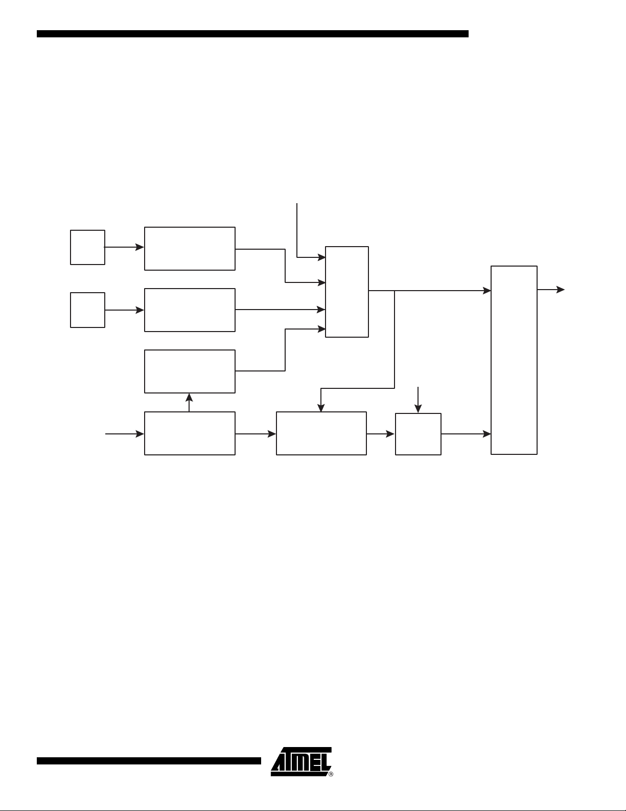
Figure 9. Reset Logic
AT43USB355
When the USB hardware is reset, the compound device is de-configured and has to be reenumerated by the host. When the microcontroller is reset, all I/O registers are then set to their
initial values, and the program starts execution from address $000. The instruction placed in
address $000 must be a JMP instruction to the reset handling routine. If the program never
enables an interrupt source, the interrupt vectors are not used, and regular program code can
be placed at these locations. The circuit diagram in Figure 9 shows the reset logic.
USB Reset
VCC
RSTN
1 MHz Clock
POR Ckt
Reset Ckt
Watchdog Timer
Divider
14-bit Cntr
OR
Cntr Reset
FSTRT
ON
S
R
Power-on Reset A Power-on Reset (POR) circuit ensures that the device is reset from power-on. An internal
timer clocked from the Watchdog timer oscillator prevents the MCU from starting until after a
certain period after V
rise time.
has reached the power-on threshold voltage, regardless of the V
CC
CC
2603G–USB–04/06
If the build-in start-up delay is sufficient, RESETN can be connected to V
external pull-up resistor. By holding the pin low for a period after V
has been applied, the
CC
Power-on Reset period can be extended.
directly or via an
CC
23
Page 24
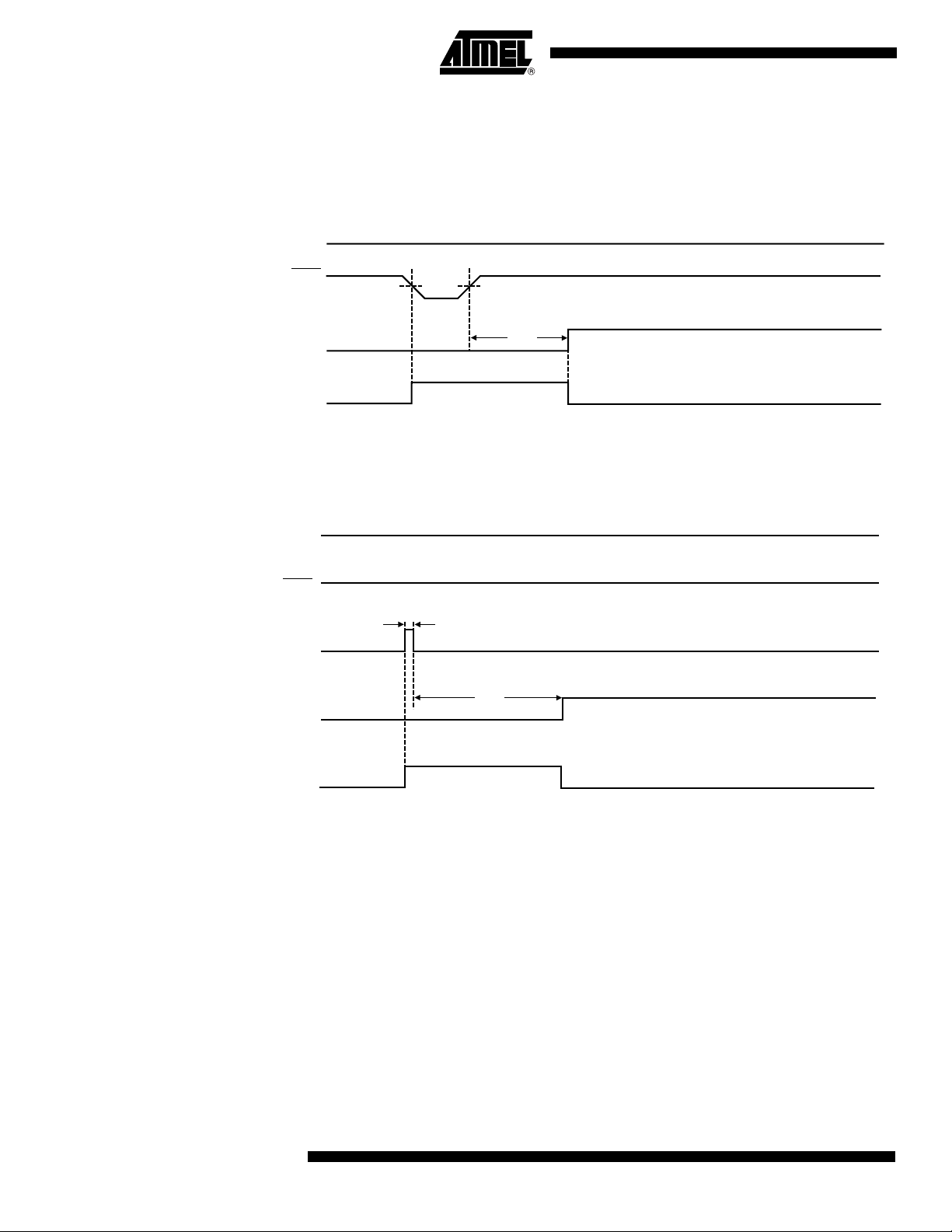
External Reset An external reset is generated by a low-level on the RESETN pin. Reset pulses longer than
200 ns will generate a reset. Shorter pulses are not guaranteed to generate a reset. When the
applied signal reaches the Reset Threshold Voltage - V
starts the MCU after the Time-out period t
has expired.
TOUT
Figure 10. External Reset During Operation
VCC
on its positive edge, the delay timer
RST
Watchdog Timer Reset
RESET
TIME-OUT
INTERNAL
RESET
V
RST
t
TOUT
When the watchdog times out, it will generate a short reset pulse of 1 XTAL cycle duration. On
the falling edge of this pulse, the delay timer starts counting the Time-out period t
TOUT
.
Figure 11. Watchdog Reset During Operation
VCC
RESET
1 XTAL Cycle
WDT
TIME-OUT
t
RESET
TIME-OUT
TOUT
Non-USB Related Interrupt Handling
24
AT43USB355
INTERNAL
RESET
The AT43USB355 has two non-USB 8-bit Interrupt Mask control registers; GIMSK (General
Interrupt Mask Register) and TIMSK (Timer/Counter Interrupt Mask Register).
When an interrupt occurs, the Global Interrupt Enable I-bit is cleared (zero) and all interrupts
are disabled. The user software can set (one) the I-bit to enable nested interrupts. The I-bit is
set (one) when a Return from Interrupt instruction, RETI, is executed.
For Interrupts triggered by events that can remain static (e.g. the Output Compare register1
matching the value of Timer/Counter1) the interrupt flag is set when the event occurs. If the
interrupt flag is cleared and the interrupt condition persists, the flag will not be set until the
event occurs the next time.
When the Program Counter is vectored to the actual interrupt vector in order to execute the
interrupt handling routine, hard-ware clears the corresponding flag that generated the interrupt. Some of the interrupt flags can also be cleared by writing a logic one to the flag bit
position(s) to be cleared.
2603G–USB–04/06
Page 25

AT43USB355
If an interrupt condition occurs when the corresponding interrupt enable bit is cleared (zero),
the interrupt flag will be set and remembered until the interrupt is enabled, or the flag is
cleared by software.
If one or more interrupt conditions occur when the global interrupt enable bit is cleared (zero),
the corresponding interrupt flag(s) will be set and remembered until the global interrupt enable
bit is set (one), and will be executed by order of priority.
Note that external level interrupt does not have a flag, and will only be remembered for as long
as the interrupt condition is active.
2603G–USB–04/06
25
Page 26

General Interrupt Mask Register – GIMSK
Bit 7 6 5 4 3 210
$3B ($5B)
Read/Write R/W R/W R R R R R R
Initial Value 0 0 0 0 0 0 0 0
INT1 INT0 – – – – – –
GIMSK
• Bit 7 – INT1: External Interrupt Request 1 Enable
When the INT1 bit is set (one) and the I-bit in the Status Register (SREG) is set (one), the
external pin interrupt is enabled. The Interrupt Sense Control1 bits 1/0 (ISC11 and ISC10) in
the MCU general Control Register (MCUCR) defines whether the external interrupt is activated on rising or falling edge of the INT1 pin or level sensed. Activity on the pin will cause an
interrupt request even if INT1 is configured as an output. The corresponding interrupt of External Interrupt Request 1 is executed from program memory address $004. See also “External
Interrupts” on page 29.
• Bit 6 – INT0: Interrupt Request 0 (Suspend/Resume Interrupt) Enable
When the INT0 bit is set (one) and the I-bit in the Status Register (SREG) is set (one), the
external pin interrupt is enabled. The Interrupt Sense Control0 bits 1/0 (ISC01 and ISC00) in
the MCU general Control Register (MCUCR) defines whether the external interrupt is activated on rising or falling edge of the INT0 pin or level sensed. Activity on the pin will cause an
interrupt request even if INT0 is configured as an output. The corresponding interrupt of Interrupt Request 0 is executed from program memory address $002. See also “External
Interrupts” on page 29.
• Bits 5..0 – Res: Reserved Bits
These bits are reserved bits in the AT43USB355 and always read as zero.
General Interrupt Flag Register – GIFR
Bit 7 6 543210
$3A ($5A) INTF1 INT F0 – – – – – – GIFR
Read/Write R/W R/W R R R R R R
Initial Value 0 0 0 0 0 0 0 0
• Bit 7 – INTF1: External Interrupt Flag1
When an event on the INT1 pin triggers an interrupt request, INTF1 becomes set (one). If the
I-bit in SREG and the INT1 bit in GIMSK are set (one), the MCU will jump to the interrupt vector at address $004. The flag is cleared when the interrupt routine is executed. Alternatively,
the flag can be cleared by writing a logical one to it.
• Bit 6 – INTF0: Interrupt Flag0 (Suspend/Resume Interrupt Flag)
When an event on the INT0 (that is, a USB event-related interrupt) triggers an interrupt
request, INTF0 becomes set (one). If the I-bit in SREG and the INT0 bit in GIMSK are set
(one), the MCU will jump to the interrupt vector at address $002. The flag is cleared when the
interrupt routine is executed. Alternatively, the flag can be cleared by writing a logical one to it.
• Bits 5..0 – Res: Reserved Bits
These bits are reserved bits in the AT43USB355 and always read as zero.
26
AT43USB355
2603G–USB–04/06
Page 27

AT43USB355
Timer/Counter Interrupt Mask Register – TIMSK
Bit 7 6 5 4 3 210
$39 ($59) TOIE1 OCIE1A OCIE1NB – TICIE1 – TOIE0 – TIMSK
Read/Write R/W R/W R/W R R/W R R/W R
Initial Value 0 0 0 0 0 0 0 0
• Bit 7 – TOIE1: Timer/Counter1 Overflow Interrupt Enable
When the TOIE1 bit is set (one) and the I-bit in the Status Register is set (one), the
Timer/Counter1 Overflow interrupt is enabled. The corresponding interrupt (at vector $006) is
executed if an overflow in Timer/Counter1 occurs, i.e., when the TOV1 bit is set in the
Timer/Counter Interrupt Flag Register (TIFR).
• Bit 6 – OCE1A: Timer/Counter1 Output CompareA Match Interrupt Enable
When the OCIE1A bit is set (one) and the I-bit in the Status Register is set (one), the
Timer/Counter1 CompareA Match interrupt is enabled. The corresponding interrupt (at vector
$004) is executed if a CompareA match in Timer/Counter1 occurs, i.e., when the OCF1A bit is
set in the TIFR.
• Bit 5 – OCIE1B: Timer/Counter1 Output CompareB Match Interrupt Enable
When the OCIE1B bit is set (one) and the I-bit in the Status Register is set (one), the
Timer/Counter1 CompareB Match interrupt is enabled. The corresponding interrupt (at vector
$005) is executed if a CompareB match in Timer/Counter1 occurs, i.e., when the OCF1B bit is
set in the TIFR.
• Bit 4 – Res: Reserved Bit
This bit is a reserved bit in the AT43USB355 and always reads zero.
• Bit 3 – TICIE1: Timer/Counter1 Input Capture Interrupt Enable
When the TICIE1 bit is set (one) and the I-bit in the Status Register is set (one), the
Timer/Counter1 Input Capture Event Interrupt is enabled. The corresponding interrupt (at vector $003) is executed if a capture-triggering event occurs on pin 31, ICP, i.e., when the ICF1
bit is set in the TIFR.
• Bit 2 – Res: Reserved Bit
This bit is a reserved bit in the AT43USB355 and always reads zero.
• Bit 1 – TOIE0: Timer/Counter0 Overflow Interrupt Enable
When the TOIE0 bit is set (one) and the I-bit in the Status Register is set (one), the
Timer/Counter0 Overflow interrupt is enabled. The corresponding interrupt (at vector $007) is
executed if an overflow in Timer/Counter0 occurs, i.e., when the TOV0 bit is set in the TIFR.
• Bit 0 – Res: Reserved Bit
This bit is a reserved bit in the AT43USB355 and always reads zero.
2603G–USB–04/06
27
Page 28

Timer/Counter Interrupt Flag Register – TIFR
Bit 7 6 5 4 3 210
$38 ($58) TOV1 OCF1A OCIFB – ICF1 – TOV0 – TIFR
Read/Write R/W R/W R/W R R/W R R/W R
Initial Value 0 0 0 0 0 0 0 0
• Bit 7 – TOV1: Timer/Counter1 Overflow Flag
The TOV1 is set (one) when an overflow occurs in Timer/Counter1. TOV1 is cleared by the
hardware when executing the corresponding interrupt handling vector. Alternatively, TOV1 is
cleared by writing a logic one to the flag. When the I-bit in SREG, and TOIE1 (Timer/Counter1
Overflow Interrupt Enable), and TOV1 are set (one), the Timer/Counter1 Overflow Interrupt is
executed. In PWM mode, this bit is set when Timer/Counter1 changes counting direction at
$0000.
• Bit 6 – OCF1A: Output Compare Flag 1A
The OCF1A bit is set (one) when compare match occurs between the Timer/Counter1 and the
data in OCR1A - Output Compare Register 1A. OCF1A is cleared by the hardware when executing the corresponding interrupt handling vector. Alternatively, OCF1A is cleared by writing a
logic one to the flag. When the I-bit in SREG, and OCIE1A (Timer/Counter1 Compare match
InterruptA Enable), and the OCF1A are set (one), the Timer/Counter1 Compare A match Interrupt is executed.
• Bit 5 – OCF1B: Output Compare Flag 1B
The OCF1B bit is set (one) when compare match occurs between the Timer/Counter1 and the
data in OCR1B - Output Compare Register 1B. OCF1B is cleared by the hardware when executing the corresponding interrupt handling vector. Alternatively, OCF1B is cleared by writing a
logic one to the flag. When the I-bit in SREG, and OCIE1B (Timer/Counter1 Compare match
InterruptB Enable), and the OCF1B are set (one), the Timer/Counter1 Compare B match Interrupt is executed.
• Bit 4 – Res: Reserved Bit
28
This bit is a reserved bit in the AT43USB355 and always reads zero.
• Bit 3 – ICF1: - Input Capture Flag 1
The ICF1 bit is set (one) to flag an input capture event, indicating that the Timer/Counter1
value has been transferred to the input capture register - ICR1. ICF1 is cleared by the hardware when executing the corresponding interrupt handling vector. Alternatively, ICF1 is
cleared by writing a logic one to the flag. When the SREG I-bit, and TICIE1 (Timer/Counter1
Input Capture Interrupt Enable), and ICF1 are set (one), the Timer/Counter1 Capture Interrupt
is executed.
• Bit 2 – Res: Reserved Bit
This bit is a reserved bit in the AT43USB355 and always reads zero.
• Bit 1 – TOV: Timer/Counter0 Overflow Flag
The bit TOV0 is set (one) when an overflow occurs in Timer/Counter0. TOV0 is cleared by the
hardware when executing the corresponding interrupt handling vector. Alternatively, TOV0 is
cleared by writing a logic one to the flag. When the SREG I- bit, and TOIE0 (Timer/Counter0
Overflow Interrupt Enable), and TOV0 are set (one), the Timer/Counter0 Overflow interrupt is
executed.
• Bit 0 – Res: Reserved Bit
This bit is a reserved bit in the AT43USB355 and always reads zero.
AT43USB355
2603G–USB–04/06
Page 29

AT43USB355
External Interrupts The external interrupts are triggered by the INT0 and INT1 pins. Observe that, if enabled, the
INT0/INT1 interrupt will trigger even if the INT0/INT1 pin is configured as an output. This feature provides a way of generating a software interrupt. The external interrupts can be triggered
by a falling or rising edge or a low level. This is set up as indicated in the specification for the
MCU Control Register (MCUCR) and the Interrupt Sense Control Register (ISCR). When
INT0/INT1 is enabled and is configured as level triggered, the interrupt will trigger as long as
the pin is held low. INT0/INT1 is set up as described in the specification for the MCU Control
Register (MCUCR).
Interrupt Response Time
The interrupt execution response for all the enabled AVR interrupts is 4 clock cycles minimum.
4 clock cycles after the interrupt flag has been set, the program vector address for the actual
interrupt handling routine is executed. During this 4 clock cycle period, the Program Counter (2
bytes) is pushed onto the Stack, and the Stack Pointer is decremented by 2. The vector is normally a jump to the interrupt routine, and this jump takes 3 clock cycles. If an interrupt occurs
during execution of a multi-cycle instruction, this instruction is completed before the interrupt is
served.
A return from an interrupt handling routine (same as for a subroutine call routine) takes 4 clock
cycles. During these 4 clock cycles, the Program Counter (2 bytes) is popped back from the
Stack, the Stack Pointer is incremented by 2, and the I flag in SREG is set. When the AVR
exits from an interrupt, it will always return to the main program and execute one more instruction before any pending interrupt is served.
2603G–USB–04/06
29
Page 30

MCU Control Register – MCUCR
Bit 7 6 5 4 3 2 1 0
$35 ($55) – – SE SM ISC11 ISC10 ISC01 ISC00 MCUCR
Read/Write R R R/W R/W R/W R/W R/W R/W
Initial Value 0 0 0 0 0 0 0 0
• Bit 7, 6 – Res: Reserved Bits
• Bit 5 – SE: Sleep Enable
The SE bit must be set (1) to make the MCU enter the sleep mode when the SLEEP instruction is executed. To avoid the MCU entering the sleep mode, unless it is the programmer's
purpose, it is recommended to set the Sleep Enable SE bit just before the execution of the
SLEEP instruction.
• Bit 4 – SM: Sleep Mode
This bit selects between the two available sleep modes. When SM is cleared (zero), Idle Mode
is selected as Sleep Mode. When SM is set (1), Power Down mode is selected as sleep mode.
The AT43USB355 does not support the Idle Mode and SM should always be set to one when
entering the Sleep Mode.
• Bit 3, 2 – ISC11, ISC10: Interrupt Sense Control 1 Bit 1 and Bit 0
The External Interrupt 1 is activated by the external pin INT1 if the SREG I-flag and the corresponding interrupt mask in the GIMSK is set. The level and edges on the external INT1 pin
that activate the interrupt are defined in the following table:
Table 7. INT1 Sense Control
ISC11 ISC10 Description
0 0 The low level of INT1 generates an interrupt request.
01Reserved.
1 0 The falling edge of INT1 generates an interrupt request.
1 1 The rising edge of INT1 generates an interrupt request.
• Bit 1, 0 – ISC01, ISC00: Interrupt Sense Control 0 bit 1 and bit 0
The External Interrupt 0 is activated by the external pin INT0 if the SREG I-flag and the corresponding interrupt mask in the GIMSK is set. The level and edges on the external INT0 pin
that activate the interrupt are defined in the following table:
Table 8. INT1 Sense Control
ISC01 ISC00 Description
0 0 The low level of INT0 generates an interrupt request.
01Reserved.
1 0 The falling edge of INT0 generates an interrupt request.
1 1 The rising edge of INT0 generates an interrupt request.
30
AT43USB355
2603G–USB–04/06
Page 31

AT43USB355
USB Interrupt Sources
The USB interrupts are described below.
Table 9. USB Interrupt Sources
Interrupt Description
SOF Received Whenever USB hardware decodes a valid Start of Frame. The
frame number is stored in the two Frame Number Registers.
EOF2 Activated whenever the hub's frame timer reaches its EOF2 time
point.
Function EP0 Interrupt See “Control Transfers at Control End-point EP0” on page 75 for
details.
Function EP1 Interrupt For an OUT end-point it indicates that Function End-point 1 has
received a valid OUT packet and that the data is in the FIFO. For
an IN end-point it means that the end-point has received an IN
token, sent out the data in the FIFO and received an ACK from the
Host. The FIFO is now ready to be written by new data from the
microcontroller.
Function EP2 Interrupt For an OUT end-point it indicates that Function End-point 2 has
received a valid OUT packet and that the data is in the FIFO. For
an IN end-point it means that the end-point has received an IN
token, sent out the data in the FIFO and received an ACK from the
Host. The FIFO is now ready to be written by new data from the
microcontroller.
Function EP3 Interrupt For an OUT end-point it indicates that Function End-point 3 has
received a valid OUT packet and that the data is in the FIFO. For
an IN end-point it means that the end-point has received an IN
token, sent out the data in the FIFO and received an ACK from the
Host. The FIFO is now ready to be written by new data from the
microcontroller.
Hub EP0 Interrupt See “Control Transfers at Control End-point EP0” on page 75 for
details.
FRWUP USB hardware has received a embedded function remote wakeup
request.
2603G–USB–04/06
GLB SUSP USB hardware has received global suspend signaling and is
preparing to put the hub in the suspend mode. The
microcontroller's firmware should place the embedded function in
the suspend state.
RSM USB hardware received resume signaling and is propagating the
resume signaling. The microcontroller's firmware should take the
embedded function out of the suspended state.
BUS RESET USB hardware received a USB bus reset. This applies only in
cases where a separation between USB bus reset and
microcontroller reset is required. Be very careful when using this
feature.
All interrupts have individual enable, status, and mask bits through the interrupt enable register and interrupt mask register. The Suspend and Resume interrupts are cleared by writing a 0
to the particular interrupt bit. All other interrupts are cleared when the microcontroller sets a bit
in an interrupt acknowledge register.
31
Page 32

USB End-point Interrupt Sources
An assertion or activation of one or more bits in the end-point's Control and Status Register
triggers the end-point interrupts. These triggers are different for control and non-control endpoints as described in the table below. Please refer to the Control and Status Register for
more information.
Table 10. USB End-point Interrupt Sources
Bit End-point type
RX_OUT_PACKET CONTROL, OUT
TX_COMPLETE CONTROL, IN
STALL_SENT CONTROL, IN
RX_SETUP CONTROL
USB Interrupt Status Register – UISR
Bit 7 6 5 4 3 2 1 0
$1FF7 SOF INT EOF2 INT – FE3 INT HEP0 INT FE2 INT FE1 INT FE0 INT UISR
Read/Write R R R R R R R R
Initial Value 0 0 0 0 0 0 0 0
• Bit 7 – SOF INT: Start of Frame Interrupt
This bit is asserted after the USB hardware receives a valid SOF packet.
• Bit 6 – EOF2 INT: EOF2 Interrupt
This bit is asserted 10 clocks before the expected start of a frame.
• Bit 5 – Res: Reserved Bit
This bit is reserved and always reads as zero.
• Bit 4 – FEP3 INT: Function End-point 3 Interrupt
• Bit 3 – HEP0 INT: Hub End-point 0 Interrupt
• Bit 2 – FEP2 INT: Function End-point 2 Interrupt
• Bit 1 – FEP1 INT: Function End-point 1 Interrupt
• Bit 0 – FEP0 INT: Function End-point 0 Interrupt
The hub and function interrupt bits will be set by the hardware whenever the following bits in
the corresponding end-point's Control and Status Register are modified by the USB hardware:
1. RX OUT Packet is set (control and OUT end-points)
2. TX Packet Ready is cleared AND TX Complete is set (control and IN end-points)
3. RX SETUP is set (control end-points only)
4. TX Complete is set
32
AT43USB355
2603G–USB–04/06
Page 33

AT43USB355
USB Interrupt Mask Register – UIMSKR
Bit 7 6 5 4 3 2 1 0
$1FF6 SOF IMSK EOF2 IMSK – FEP3 IMSK HEP0 IMSK FEP2 IMSK FEP1 IMSK FEP0 IMSK UIMSKR
Read/Write R/W R/W R R/W R/W R/W R/W R/W
Initial Value 0 0 0 0 0 0 0 0
• Bit 7 – SOF IMSK: Start of Frame Interrupt Mask
When the SOF IMSK bit is set (1), the Start of Frame Interrupt is masked.
• Bit 6 – EOF2 IMSK: EOF2 Interrupt Mask
When the EOF2 IMSK bit is set (1), the EOF2 Interrupt is masked.
• Bit 5 – Res: Reserved bit
This bit is reserved and always read as zero.
• Bit 4 – FEP3 IMSK: Function End-point 3 Interrupt Mask
When the FE3 IMSK bit is set (1), the Function End-point 3 Interrupt is masked.
• Bit 3 – HEP0 IMSK: End-point 0 Interrupt Mask
When the HEP0 IMSK bit is set (1), the Hub End-point 0 Interrupt is masked.
• Bit 2 – FEP2 IMSK: End-point 2 Interrupt Mask
When the FE2 IMSK bit is set (1), the Function End-point 2 Interrupt is masked.
• Bit 1 – FEP1 IMSK: End-point 1 Interrupt Mask
When the FE1 IMSK bit is set (1), the Function End-point 1 Interrupt is masked.
• Bit 0 – FEP0 IMSK: End-point 0 Interrupt Mask
When the FE0 IMSK bit is set (1), the Function End-point 0 Interrupt is masked.
2603G–USB–04/06
33
Page 34

USB Interrupt Acknowledge Register – UIAR
Bit 7 6 5 4 3 2 1 0
$1FF5 SOF INTACK EOF2 INTACK – FEP3 INTACK HEP0 INTACK FEP2 IMSK FEP1 INTACK FEP0 INTACK UIAR
Read/Write W W R W W W W W
Initial Value 0 0 0 0 0 0 0 0
• Bit 7 – SOF INTACK: Start of Frame Interrupt Acknowledge
The microcontroller firmware writes a 1 to this bit to clear the SOF INT bit.
• Bit 6 – EOF2 INTACK: EOF2 Interrupt Acknowledge
The microcontroller firmware writes a 1 to this bit to clear the EOF2 INT bit.
• Bit 5 – Res: Reserved bit
This bit is reserved and is always read as zero.
• Bit 4 – FEP3 INTACK: Function End-point 3 Interrupt Acknowledge
The microcontroller firmware writes a 1 to this bit to clear the FEP3 INT bit.
• Bit 3 – HEP0 INTACK: Hub End-point 0 Interrupt Acknowledge
The microcontroller firmware writes a 1 to this bit to clear the HEP0 INT bit.
• Bit 2 – FEP2 INTACK: Function End-point 2 Interrupt Acknowledge
The microcontroller firmware writes a 1 to this bit to clear the FEP2 bit.
• Bit 1 – FEP1 INTACK: Function End-point 1 Interrupt Acknowledge
The microcontroller firmware writes a 1 to this bit to clear the FEP1 bit.
• Bit 0 – FEP0 INTACK: Function End-point 0 Interrupt Acknowledge
The microcontroller firmware writes a 1 to this bit to clear the FEP0 INT bit.
34
AT43USB355
2603G–USB–04/06
Page 35

AT43USB355
USB Interrupt Enable Register – UIER
Bit 7 6 5 4 3 2 1 0
$1FF3 SOF IE EOF2 IE – FEP3 IE HEP0 IE FEP2 IE FEP1 IE FEP0 IE UIER
Read/Write R/W R/W R R/W R/W R/W R/W R/W
Initial Value 0 0 0 0 0 0 0 0
• Bit 7 – SOF IE: Enable Start of Frame Interrupt
When the SOF IE bit is set (1), the Start of Frame Interrupt is enabled.
• Bit 6 – EOF2 IE: Enable EOF2 Interrupt
When the EOF2 IE bit is set (1), the EOF2 Interrupt is enabled.
• Bit 5 – Res: Reserved bit
This bit is reserved and always read as zero.
• Bit 4 – FEP3 IE: Enable Function End-point 3 Interrupt
When the FE3 IE bit is set (1), the Function End-point 3 Interrupt is enabled.
• Bit 3 – HEP0 IE: Enable End-point 0 Interrupt
When the HEP0 IE bit is set (1), the Hub End-point 0 Interrupt is enabled.
• Bit 2 – FEP2 IE: Enable End-point 2 Interrupt
When the FE2 IE bit is set (1), the Function End-point 2 Interrupt is enabled.
• Bit 1 – FEP1 IE: Enable End-point 1 Interrupt
When the FE1 IE bit is set (1), the Function End-point 1 Interrupt is enabled.
• Bit 0 – FEP0 IE: Enable End-point 0 Interrupt
When the FE0 IE bit is set (1), the Function End-point 0 Interrupt is enabled.
Suspend/Resume Register – SPRSR
Bit76 543 2 1 0
$1FFA – – – – BUS INT FRWUP RSM GLB SUSP SPRSR
Read/Write R R R R R/W R R R
Initial Value 0 0 0 0 0 0 0 0
• Bit 7..4 – Res: Reserved Bits
These bits are reserved and are always read as zeros.
• Bit 3 – BUS INT: USB Bus Interrupt
When the USB reset separation feature is enabled (SPRSIE and SPRSMSK bits 3 are set to
1) the BUS INT bit is set when USB bus reset is detected by the USB hardware.
• Bit 2 – FRWUP: Function Remote Wakeup
The USB hardware sets this bit to signal that External Interrupt 1 is detected indicating remote
wakeup. An interrupt is generated if the FRWUP IE bit of the SPRSIE register is set.
• Bit 1 – RSM: Resume
2603G–USB–04/06
The USB hardware sets this bit when a USB resume signaling is detected at any of its port
except Port 1. An interrupt is generated if the RSM IE bit of the SPRSIE register is set.
• Bit 0 – GLB SUSP: Global Suspend
The USB hardware sets this bit when a USB global suspend signaling is detected. An interrupt
is generated if the GLBSUSP IE bit of the SPRSIE register is set.
35
Page 36

Suspend/Resume Interrupt Enable Register – SPRSIE
Bit 7 6 5 4 3 2 1 0
$1FF9 – – – – BUS INT FRWUP RSM GLB SUSP SPRSIE
Read/Write R R R R R/W R R R
Initial Value 0 0 0 0 0 0 0 0
• Bit 7..4 – Res: Reserved Bits
These bits are reserved and are always read as zeros.
• Bit 3 – BUS INT EN: USB Reset Interrupt Enable
When the BUS INT EN bit is set, the USB and microcontroller resets are separated. A USB
bus reset (SE0 for longer than 3 ms) will reset the USB hardware only and not the microcontroller. However, an interrupt to the microcontroller will be generated and bit 3 of SPRSR is
set.
• Bit 2 – FRWUP IE: Function Remote Wakeup Interrupt Enable
Setting the FRWUP IE bit will initiate an interrupt whenever the FRWUP bit of SPRSR is set.
• Bit 1 – RSM IE: Resume Interrupt Enable
Setting the RSM IE bit will initiate an interrupt whenever the RSM bit of SPRSR is set.
• Bit 0 – GLB SUSP IE: Global Suspend Interrupt Enable
Setting the GLB SUSP IE bit will initiate an interrupt whenever the GLB SUSP bit of SPRSR is
set.
Suspend/Resume Interrupt Mask Register – SPRSMSK
Bit 7 6 5 4 3 2 1 0
$1FF8 – – – – BUS INT MSK FRWUP MSK RSM GLB SUSP SPRSMSK
Read/Write R R R R W W W W
Initial Value 0 0 0 0 0 0 0 0
The bits of the Suspend/Resume Mask Register are used to make an interrupt caused by an
event in the Suspend/Resume Register visible to the microcontroller. The Suspend/Resume
Interrupt Enable Register bits enable the interrupt while the Suspend/Resume Interrupt Mask
Register allows the microcontroller to control when it wants visibility to an interrupt. 1 = Enable
Mask, 0 = Disable Mask.
• Bit 7..4 – Res: Reserved Bits
These bits are reserved and are always read as zeros.
• Bit 3 – BUS INT MSK: USB Reset Interrupt Mask
• Bit 2 – FRWUP MSK: Function Remote Wakeup Interrupt Mask
• Bit 1 – RSM MSK: Resume Interrupt Mask
• Bit 0 – GLB SUSP MSK: Global Suspend Interrupt Enable
36
AT43USB355
2603G–USB–04/06
Page 37

AVR Register Set
Status Register and Stack Pointer
Status Register – SREG
Bit 7 6 5 4 3 2 1 0
$3F ($5F) ITHSVNZCSREG
Read/Write R/W R/W R/W R/W R/W R/W R/W R/W
Initial Value 0 0 0 0 0 0 0 0
•Bit 7 – I: Global Interrupt Enable
The global interrupt enable bit must be set (one) for the interrupts to be enabled. The individual interrupt enable control is then performed in separate control registers. If the global
interrupt enable bit is cleared (zero), none of the interrupts are enabled independent of the
individual interrupt enable settings. The I-bit is cleared by the hardware after an interrupt has
occurred, and is set by the RETI instruction to enable subsequent interrupts.
•Bit 6 – T: Bit Copy Storage
The bit copy instructions BLD (Bit LoaD) and BST (Bit STore) use the T bit as source and destination for the operated bit. A bit from a register in the register file can be copied into T by the
BST instruction, and a bit in T can be copied into a bit in a register in the register file by the
BLD instruction.
•Bit 5 – H: Half Carry Flag
AT43USB355
The half carry flag H indicates a half carry in some arithmetic operations. See the Instruction
Set Description for detailed information.
•Bit 4 – S: Sign Bit, S = N⊕V
The S-bit is always an exclusive or between the negative flag N and the two's complement
overflow flag V. See the Instruction Set Description for detailed information.
•Bit 3 – V: Two's Complement Overflow Flag
The two's complement overflow flag V supports two's complement arithmetics. See the
Instruction Set Description for detailed information.
•Bit 2 – N: Negative Flag
The negative flag N indicates a negative result after the different arithmetic and logic operations. See the Instruction Set Description for detailed information.
•Bit 1 – Z: Zero Flag
The zero flag Z indicates a zero result after the different arithmetic and logic operations. See
the Instruction Set Description for detailed information.
•Bit 0 – C: Carry Flag
The carry flag C indicates a carry in an arithmetic or logic operation. See the Instruction Set
Description for detailed information.
Note that the status register is not automatically stored when entering an interrupt routine and
restored when returning from an interrupt routine. This must be handled by software.
2603G–USB–04/06
37
Page 38

Stack Pointer Register – SP
Bit 1514 131211109 8
$3E ($5E) ITHSVNZCSPH
$3D ($5D) SP7 SP6 SP5 SP4 SP3 SP2 SP1 SP0 SPL
76 5 4 3210
Read/Write R/W R/W R/W R/W R/W R/W R/W R/W
R/W R/W R/W R/W R/W R/W R/W R/W
Initial Value 0 0 0 0 0 0 0 0
00 0 0 0000
The Stack Pointer points to the data SRAM stack area where the Subroutine and Interrupt
Stacks are located. This Stack space in the data SRAM must be defined by the program
before any subroutine calls are executed or interrupts are enabled. The stack pointer must be
set to point above $60. The Stack Pointer is decremented by one when data is pushed onto
the Stack with the PUSH instruction, and it is decremented by two when an address is pushed
onto the Stack with subroutine calls and interrupts. The Stack Pointer is incremented by one
when data is popped from the Stack with the POP instruction and it is incremented by two
when an address is popped from the Stack with return from subroutine RET or return from
interrupt RETI.
Sleep Modes To enter the sleep modes, the SE bit in MCUCR must be set (one) and a SLEEP instruction
must be executed. If an enabled interrupt occurs while the MCU is in a sleep mode, the MCU
awakes, executes the interrupt routine, and resumes execution from the instruction following
SLEEP. The contents of the register file, SRAM and I/O memory are unaltered. If a reset
occurs during sleep mode, the MCU wakes up and executes from the Reset vector.
Power Down Mode When the SM bit is set (one), the SLEEP instruction forces the MCU into the Power Down
Mode. In this mode, the external oscillator is stopped, while the external interrupts continue
operating. Only an external reset, an external level interrupt on INT0 or INT1, can wake up the
MCU.
Note that when a level triggered interrupt is used for wake-up from power down, the low level
must be held for a time longer than the reset delay time-out period t
. Otherwise, the MCU
TOUT
will fail to wake up.
38
AT43USB355
2603G–USB–04/06
Page 39
AT43USB355
Timer/Counters The AT43USB355 provides two general-purpose Timer/Counters - one 8-bit T/C and one 16-
bit T/C. The Timer/Counters have individual prescaling selection from the same 10-bit prescaling timer. Both Timer/Counters can either be used as a timer with an internal clock timebase or
as a counter with an external pin connection which triggers the counting.
Timer/Counter Prescaler
The four different prescaled selections are: CK/8, CK/64, CK/256 and CK/1024 where CK is
the oscillator clock. For the two Timer/Counters, added selections as CK, external source and
stop, can be selected as clock sources.
Figure 12. Timer/Counter Prescaler
CK
T0
T1
0
10-bit T/C Prescaler
CK/8
CK/64
0
CK/256
CK/1024
CS10
CS11
CS12
2603G–USB–04/06
Timer/Counter1 Clock Source
TCK1
CS00
CS01
CS02
Timer/Counter0 Clock Source
TCK0
39
Page 40

8-bit Timer/Counter0
The 8-bit Timer/Counter0 can select clock source from CK, prescaled CK or an external pin. In
addition it can be stopped as described in the specification for the Timer/Counter0 Control
Register (TCCR0). The overflow status flag is found in the Timer/Counter Interrupt Flag Register (TIFR). Control signals are found in the Timer/Counter0 Control Register (TCCR0). The
interrupt enable/disable settings for Timer/Counter0 are found in the Timer/Counter Interrupt
Mask Register - TIMSK.
When Timer/Counter0 is externally clocked, the external signal is synchronized with the oscillator frequency of the CPU. To assure proper sampling of the external clock, the minimum
time between two external clock transitions must be at least one internal CPU clock period.
The external clock signal is sampled on the rising edge of the internal CPU clock.
The 8-bit Timer/Counter0 features both a high resolution and a high accuracy usage with the
lower prescaling opportunities. Similarly, the high prescaling opportunities make the
Timer/Counter0 useful for lower speed functions or exact timing functions with infrequent
actions.
Figure 13. Timer/Counter0 Block Diagram
T/C0
Overflow IRQ
8-bit Data Bus
TOIE1
OICIE1A
OICIE1B
TICIE1
TOIE0
Timer Int. Mask Register
(TIMSK)
70
Timer/Counter0
(TCNT0)
Timer Int. Flag Register
TOV1
OCF1A
T/C Clock Source
(TIFR)
OCF1B
TOV0
ICF1
T/C0 Control Register
(TCCR0)
CS02
CS01
TOV0
Control
Logic
CS00
CK
T0
40
AT43USB355
2603G–USB–04/06
Page 41
AT43USB355
Timer/Counter0 Control Register – TCCR0
Bit7654321 0
$33 ($53) – – – – – CS02 CS01 CS00 TCCR0
Read/Write R R R R R R/W R/W R/W
Initial Value 0 0 0 0 0 0 0 0
• Bits 7..3 – Res: Reserved Bits
These bits are reserved bits in the AT43USB355 and always read as zero.
• Bits 2, 1, 0 – CS02, CS01, CS00: Clock Select0, bit 2, 1 and 0
The Clock Select0 bits 2, 1 and 0 define the prescaling source of Timer/Counter0.
Table 11. Clock 0 Prescale Select
CS02 CS01 CS00 Description
0 0 0 Stop, the Timer/Counter0 is stopped
001CK
010CK/8
011CK/64
100CK/256
101CK/1024
1 1 0 External Pin T0, falling edge
1 1 1 External Pin T0, rising edge
The Stop condition provides a Timer Enable/Disable function. The CK down divided modes
are scaled directly from the CK oscillator clock. If the external pin modes are used for
Timer/Counter0, transitions on PB0/(T0) will clock the counter even if the pin is configured as
an output. This feature can give the user SW control of the counting.
Timer/Counter0 – TCNT0
Bit 7 6 5 4 3 2 1 0
$32 ($52) MSB – – – – – – LSB TCNT0
Read/Write R/W R/W R/W R/W R/W R/W R/W R/W
Initial Value 0 0 0 0 0 0 0 0
The Timer/Counter0 is realized as an up-counter with read and write access. If the
Timer/Counter0 is written and a clock source is present, the Timer/Counter0 continues counting in the clock cycle following the write operation.
2603G–USB–04/06
41
Page 42

16-bit Timer/Counter1
Figure 14. Timer/Counter1 Block Diagram
T/C1
OVERFLOW IRQ
TOIE1
OCIE1A
OCIE1B
TICIE1
8-BIT DATA BUS
TIMER INT. MASK
REGISTER (TIMSK)
15
T/C1 INPUT CAPTURE REGISTER (ICR1)
TOIE0
8
T/C1 COMPARE
MATCHA IRQ
TOV1
OCF1A
OCF1B
TIMER INT. FLAG
REGISTER (TIFR)
TOV1
OCF1A
OCF1B
7
T/C1 COMPARE
MATCHB IRQ
ICF1
TOV0
ICF1
CAPTURE
TRIGGER
T/C1 CONTROL
REGISTER A (TCCR1A)
COM1A1
COM1A0
COM1B1
0
T/C1INPUT
CAPTURE IRQ
COM1B0
PWM11
CONTROL
T/C1 CONTROL
REGISTER B (TCCR1B)
ICES1
ICNC1
PWM10
LOGIC
CS12
CTC1
CS11
CS10
CK
T1
7
15
TIMER/COUNTER1 (TCNT1)
15
16-BIT COMPARATOR
15
TIMER/COUNTER1 OUTPUT COMPARE REGISTER A
8
7
8
7
8
0
0
15
16-BIT COMPARATOR
0
TIMER/COUNTER1 OUTPUT COMPARE REGISTER B
78
7
815
0
0
42
AT43USB355
2603G–USB–04/06
Page 43

AT43USB355
16-bit Timer/Counter1 Operation
The 16-bit Timer/Counter1 can select clock source from CK, prescaled CK or an external pin.
In addition, it can be stopped as described in the specification for the Timer/Counter1 Control
Registers (TCCR1A and TCCR1B). The different status flags (overflow, compare match and
capture event) are found in the Timer/Counter Interrupt Flag Register (TIFR). Control signals
are found in the Timer/Counter1 Control Registers (TCCR1A and TCCR1B). The interrupt
enable/disable settings for Timer/Counter1 are found in the Timer/Counter Interrupt Mask
Register (TIMSK).
When Timer/Counter1 is externally clocked, the external signal is synchronized with the oscillator frequency of the CPU. To assure proper sampling of the external clock, the minimum
time between two external clock transitions must be at least one internal CPU clock period.
The external clock signal is sampled on the rising edge of the internal CPU clock.
The 16-bit Timer/Counter1 features both a high resolution and a high accuracy usage with the
lower prescaling opportunities. Similarly, the high prescaling opportunities makes the
Timer/Counter1 useful for lower speed functions or exact timing functions with infrequent
actions.
The Timer/Counter1 supports two Output Compare functions using the Output Compare Register 1 A and B (OCR1A and OCR1B) as the data sources to be compared to the
Timer/Counter1 contents. The Output Compare functions include optional clearing of the
counter on compareA match, and actions on the Output Compare pins on both compare
matches.
Timer/Counter1 can also be used as a 8-, 9- or 10-bit Pulse With Modulator. In this mode the
counter and the OCR1A/OCR1B registers serve as a dual glitch-free stand-alone PWM with
centered pulses.
The Input Capture function of Timer/Counter1 provides a capture of the Timer/Counter1 contents to the Input Capture Register - ICR1, triggered by an external event on the Input Capture
Pin (ICP/PF3). The actual capture event settings are defined by the Timer/Counter1 Control
Register (TCCR1B). The AT43USB355 has no analog comparator and the mux control signal,
ACO, is permanently set so that the ICP input is routed to the noise canceler.
If the noise canceler function is enabled, the actual trigger condition for the capture event is
monitored over 4 samples, and all 4 must be equal to activate the capture flag.
Figure 15. ICP Pin Schematic Diagram
0
ICP
1
ACIC: COMPARATOR IC ENABLE
ACC0: COMPARATOR OUTPUT
NOISE CANCELER
ICNC1 ICES1
EDGE SELECT
ICF1
ACIC
ACO
2603G–USB–04/06
43
Page 44

Timer/Counter1 Control Register A – TCCR1A
Bit 7 6 543210
$2F ($4F) COM1A1 COM1A0 COM1B1 COM1B0 – – PWM11 PWM10 TCCR1A
Read/Write R/W R/W R/W R/W R R R/W R/W
Initial Value 0 0 0 0 0 0 0 0
• Bits 7, 6 – COM1A1, COM1A0: Compare Output Mode1A, Bits 1 and 0
The COM1A1 and COM1A0 control bits determine any output pin action following a compare
match in Timer/Counter1. Any output pin actions affect pin OC1A (Output CompareA) pin 1.
This is an alternative function to an I/O port and the corresponding direction control bit must be
set (one) to control the output pin. The control configuration is shown in Table 12.
• Bits 5, 4 – COM1B1, COM1B0: Compare Output Mode1B, Bits 1 and 0
The COM1B1 and COM1B0 control bits determine any output pin action following a compare
match in Timer/Counter1. Any output pin actions affect pin OC1B (Output CompareB). The following control configuration is given:
Table 12. Compare 1 Mode Select
COM1X1 COM1X0 Description
0 0 Timer/Counter1 disconnected from output pin OC1X.
0 1 Toggle the OC1X output line.
1 0 Clear the OC1X output line (to zero).
1 1 Set the OC1X output line (to one).
Note: 1. X = A or B
2. In PWM mode, these bits have a different function. Refer to Table 16 for a detailed
description.
(2)
(1)
(1)
(1)
• Bits 3..2 – Res: Reserved Bits
These bits are reserved bits in the AT43USB355 and always read zero.
• Bits 1..0 – PWM11, PWM10: Pulse Width Modulator Select Bits 1 and 0
These bits select PWM operation of Timer/Counter1 as specified in Table 13.
Table 13. PWM Mode Select
PWM11 PWM10 Description
0 0 PWM operation of Timer/Counter1 is disabled.
0 1 Timer/Counter1 is an 8-bit PWM.
1 0 Timer/Counter1 is a 9-bit PWM.
1 1 Timer/Counter1 is a 10-bit PWM.
(1)
44
AT43USB355
2603G–USB–04/06
Page 45

AT43USB355
Timer/Counter1 Control Register B – TCCR1B
Bit 7 6 543210
$2E ($4E) ICNC1 ICES1 – – CTC1 CS12 CS11 CS10 TCCR1B
Read/Write R/W R/W R/W R/W R R R/W R/W
Initial Value 0 0 0 0 0 0 0 0
•Bit 7 – ICNC1: Input Capture1 Noise Canceler (4 CKs)
When the ICNC1 bit is cleared (zero), the input capture trigger noise canceler function is disabled. The input capture is triggered at the first rising/falling edge sampled on the ICP (input
capture pin) as specified. When the ICNC1 bit is set (one), four successive samples are measured on the ICP and all samples must be high/low according to the input capture trigger
specification in the ICES1 bit. The actual sampling frequency is the 12 MHz system clock
frequency.
•Bit 6 – ICES1: Input Capture1 Edge Select
While the ICES1 bit is cleared (zero), the Timer/Counter1 contents are transferred to the Input
Capture Register (ICR1) on the falling edge of the ICP. While the ICES1 bit is set (one), the
Timer/Counter1 contents are transferred to the ICR1 on the rising edge of the ICP.
• Bits 5, 4 – Res: Reserved Bits
These bits are reserved bits in the AT43USB355 and always read zero.
•Bit 3 – CTC1: Clear Timer/Counter1 on Compare Match
When the CTC1 control bit is set (one), the Timer/Counter1 is reset to $0000 in the clock cycle
after a compareA match. If the CTC1 control bit is cleared, Timer/Counter1 continues counting
and is unaffected by a compare match. Since the compare match is detected in the CPU clock
cycle following the match, this function will behave differently when a prescaling higher than 1
is used for the timer. When a prescaling of 1 is used, and the compareA register is set to C,
the timer will count as follows if CTC1 is set:
... | C-2 | C-1 | C | 0 | 1 | ...
When the prescaler is set to divide by 8, the timer will count like this:
... | C-2, C-2, C-2, C-2, C-2, C-2, C-2, C-2 | C-1, C-1, C-1, C-1, C-1, C-1, C-1, C-1 | C, 0, 0, 0,
0, 0, 0, 0 | ...
In PWM mode, this bit has no effect.
• Bits 2, 1, 0 – CS12, CS11, CS10: Clock Select1, Bit 2, 1 and 0
The Clock Select1 bits 2, 1 and 0 define the prescaling source of Timer/Counter1.
Table 14. Clock 1 Prescale Select
CS12 CS11 CS10 Description
0 0 0 Stop, the Timer/Counter1 is stopped.
001CK
2603G–USB–04/06
010CK/8
011CK/64
100CK/256
45
Page 46

Table 14. Clock 1 Prescale Select (Continued)
CS12 CS11 CS10 Description
101CK/1024
1 1 0 External Pin T1, falling edge
1 1 1 External Pin T1, rising edge
The Stop condition provides a Timer Enable/Disable function. The CK down divided modes
are scaled directly from the 12 MHz system clock. If the external pin modes are used for
Timer/Counter1, transitions on PB1/(T1) will clock the counter even if the pin is configured as
an output. This feature can give the user SW control of the counting.
46
AT43USB355
2603G–USB–04/06
Page 47

AT43USB355
Timer/Counter1 – TCNT1H and TCNT1L
Bit 1514 131211109 8
$2D ($4D) MSB – – – – – – – TCNT1H
$2C ($4C) – – – – – – – LSB TCNT1L
76 5 4 3210
Read/Write R/W R/W R/W R/W R/W R/W R/W R/W
R/W R/W R/W R/W R/W R/W R/W R/W
Initial Value 0 0 0 0 0 0 0 0
00 0 0 0000
This 16-bit register contains the prescaled value of the 16-bit Timer/Counter1. To ensure that
both the high and low bytes are read and written simultaneously when the CPU accesses
these registers, the access is performed using an 8-bit temporary register (TEMP). This temporary register is also used when accessing OCR1A, OCR1B and ICR1. If the main program
and also interrupt routines perform access to registers using TEMP, interrupts must be disabled during access from the main program and from interrupt routines if interrupts are
allowed from within interrupt routines.
• TCNT1 Timer/Counter1 Write:
When the CPU writes to the high byte TCNT1H, the written data is placed in the TEMP register. Next, when the CPU writes the low byte TCNT1L, this byte of data is combined with the
byte data in the TEMP register, and all 16 bits are written to the TCNT1 Timer/Counter1 register simultaneously. Consequently, the high byte TCNT1H must be accessed first for a full 16bit register write operation.
• TCNT1 Timer/Counter1 Read:
When the CPU reads the low byte TCNT1L, the data of the low byte TCNT1L is sent to the
CPU and the data of the high byte TCNT1H is placed in the TEMP register. When the CPU
reads the data in the high byte TCNT1H, the CPU receives the data in the TEMP register.
Consequently, the low byte TCNT1L must be accessed first for a full 16-bit register read
operation.
The Timer/Counter1 is realized as an up or up/down (in PWM mode) counter with read and
write access. If Timer/Counter1 is written to and a clock source is selected, the
Timer/Counter1 continues counting in the timer clock cycle after it is preset with the written
value.
2603G–USB–04/06
47
Page 48

Timer/Counter1 Output Compare Register – OCR1AH and OCR1AL
Bit 15 14 13 12 11 10 9 8
$2B ($4B) MSB–––––––OCR1AH
$2A ($4A) –––––––LSBOCR1AL
76543210
Read/Write R/W R/W R/W R/W R/W R/W R/W R/W
R/W R/W R/W R/W R/W R/W R/W R/W
Initial Value 0 0 0 0 0 0 0 0
00000000
Timer/Counter1 Output Compare Register – OCR1BH and OCR1BL
Bit 1514131211109 8
$29 ($49) MSB–––––––OCR1BH
$28 ($48) –––––––LSBOCR1BL
76543210
Read/Write R/W R/W R/W R/W R/W R/W R/W R/W
R/W R/W R/W R/W R/W R/W R/W R/W
Initial Value 0 0 0 0 0 0 0 0
00000000
The output compare registers are 16-bit read/write registers.
The Timer/Counter1 Output Compare Registers contain the data to be continuously compared
with Timer/Counter1. Actions on compare matches are specified in the Timer/Counter1 Control and Status register.A compare match does only occur if Timer/Counter1 counts to the
OCR value. A software write that sets TCNT1 and OCR1A or OCR1B to the same value does
not generate a compare match.
A compare match will set the compare interrupt flag in the CPU clock cycle following the compare event.
Since the Output Compare Registers OCR1A and OCR1B are 16-bit registers, a temporary
register TEMP is used when OCR1A/B are written to ensure that both bytes are updated
simultaneously. When the CPU writes the high byte, OCR1AH or OCR1BH, the data is temporarily stored in the TEMP register. When the CPU writes the low byte, OCR1AL or OCR1BL,
the TEMP register is simultaneously written to OCR1AH or OCR1BH. Consequently, the high
byte OCR1AH or OCR1BH must be written first for a full 16-bit register write operation.
The TEMP register is also used when accessing TCNT1, and ICR1. If the main program and
also interrupt routines perform access to registers using TEMP, interrupts must be disabled
during access from the main program and from interrupt routines if interrupts are allowed from
within interrupt routines.
48
AT43USB355
2603G–USB–04/06
Page 49

AT43USB355
Timer/Counter1 Input Capture Register – ICR1H and ICR1L
Bit 1514131211109 8
$25 ($45) MSB – – – – – – – ICR1H
$24 ($44) –– – – –––LSBICR1L
76 5 4 3210
Read/Write R R R R R R R R
RR R R RRRR
Initial Value 0 0 0 0 0 0 0 0
00 0 0 0000
The input capture register is a 16-bit read-only register.
When the rising or falling edge (according to the input capture edge setting - ICES1) of the signal at the input capture pin (ICP) is detected, the current value of the Timer/Counter1 is
transferred to the Input Capture Register (ICR1). At the same time, the Input Capture Flag
(ICF1) is set (one).
Since the ICR1 is a 16-bit register, a temporary register TEMP is used when ICR1 is read to
ensure that both bytes are read simultaneously. When the CPU reads the low byte ICR1L, the
data is sent to the CPU and the data of the high byte ICR1H is placed in the TEMP register.
When the CPU reads the data in the high byte ICR1H, the CPU receives the data in the TEMP
register. Consequently, the low byte ICR1L must be accessed first for a full 16-bit register read
operation.
Timer/Counter1 In PWM Mode
The TEMP register is also used when accessing TCNT1, OCR1A and OCR1B. If the main program and also interrupt routines perform access to registers using TEMP, interrupts must be
disabled during access from the main program and from interrupt routines, if interrupts are
allowed from within interrupt routines.
When the PWM mode is selected, Timer/Counter1, the Output Compare Register1A (OCR1A)
and the Output Compare Register1B (OCR1B) form a dual 8-, 9- or 10-bit, free-running, glitchfree and phase correct PWM with outputs on the PD5 (OC1A) and OC1B pins.
Timer/Counter1 acts as an up/down counter, counting up from $0000 to TOP (see Table 15),
where it turns and counts down again to zero before the cycle is repeated. When the counter
value matches the contents of the 10 least significant bits of OCR1A or OCR1B, the
PD5(OC1A)/OC1B pins are set or cleared according to the settings of the COM1A1/COM1A0
or COM1B1/COM1B0 bits in the Timer/Counter1 Control Register TCCR1A. Refer to Table 16
for details.
Table 15. Timer TOP Values and PWM Frequency
PWM Resolution Timer TOP value Frequency
8-bit $00FF (255) f
9-bit $01FF (511) f
10-bit $03FF(1023) f
TCK1
TCK1
TCK1
/510
/1022
/2046
2603G–USB–04/06
49
Page 50

Table 16. Compare1 Mode Select in PWM Mode
COM1X1 COM1X0 Effect on OCX1
0 0 Not connected
0 1 Not connected
10
11
Note: X = A or B
Note that in the PWM mode, the 10 least significant OCR1A/OCR1B bits, when written, are
transferred to a temporary location. They are latched when Timer/Counter1 reaches the value
TOP. This prevents the occurrence of odd-length PWM pulses (glitches) in the event of an
unsynchronized OCR1A/OCR1B write. See Figure 16 for an example.
Figure 16. Effects on Unsynchronized OCR1 Latching
Cleared on compare match, up-counting. Set on compare match,
down-counting (non-inverted PWM).
Cleared on compare match, down-counting. Set on compare match,
up-counting (inverted PWM).
Compare Value Changes
Counter Value
Compare Value
Synchronized OCR1X Latch
Unsynchronized OCR1X Latch
Note: X = A or B
PWM Output OC1X
Compare Value Changes
Counter Value
Compare Value
PWM Output OC1X
Glitch
During the time between the write and the latch operation, a read from OCR1A or OCR1B will
read the contents of the temporary location. This means that the most recently written value
always will read out of OCR1A/B
When the OCR1 contains $0000 or TOP, the output OC1A/OC1B is updated to low or high on
the next compare match, according to the settings of COM1A1/COM1A0 or
COM1B1/COM1B0. This is shown in Table 17.
Note: If the compare register contains the TOP value and the prescaler is not in use
(CS12..CS10 = 001), the PWM output will not produce any pulse at all, because up-counting
and down-counting values are reached simultaneously. When the prescaler is in use
50
AT43USB355
2603G–USB–04/06
Page 51

AT43USB355
(CS12..CS10 = 001 or 000), the PWM output goes active when the counter reaches the TOP
value, but the down-counting compare match is not interpreted to be reached before the next
time the counter reaches the TOP value, making a one-period PWM pulse.
Table 17. PWM Outputs OCR1X = $0000 or Top
COM1X1 COM1X0 OCR1X Output OC1X
1 0 $0000 L
10TOP H
1 1 $0000 H
11TOP L
Note: X = A or B
In PWM mode, the Timer Overflow Flag1, TOV1, is set when the counter advances from
$0000. Timer Overflow Interrupt1 operates exactly as in normal Timer/Counter mode, i.e. it is
executed when TOV1 is set provided that Timer Overflow Interrupt1 and global interrupts are
enabled. This also applies to the Timer Output Compare1 flags and interrupts.
Watchdog Timer The Watchdog Timer is clocked from a 1 MHz clock derived from the 6 MHz on chip oscillator.
By controlling the Watchdog Timer prescaler, the Watchdog reset interval can be adjusted,
see Table 18 for a detailed description. The WDR (Watchdog Reset) instruction resets the
Watchdog Timer. Eight different clock cycle periods can be selected to determine the reset
period. If the reset period expires without another Watchdog reset, the AT43USB355 resets
and executes from the reset vector.
To prevent unintentional disabling of the watchdog, a special turn-off sequence must be followed when the watchdog is disabled. Refer to the description of the Watchdog Timer Control
Register for details.
Figure 17. Watchdog Timer
1 MHz Clock
Watchdog
Reset
OSC/16K
WDP0
WDP1
WDP2
WDE
Watchdog Prescaler
OSC/32K
OSC/64K
OSC/128K
OSC/256K
OSC/512K
OSC/1024K
OSC/2048K
2603G–USB–04/06
MCU Reset
51
Page 52

Watchdog Timer Control Register – WDTCR
Bit 7 6 5 4 3 2 1 0
$21 ($41) – – – WDTOE WDE WDP2 WDP1 WDP0 WDTCR
Read/Write R R R R/W R/W R/W R/W R/W
Initial Value 0 0 0 0 0 0 0 0
• Bits 7..5 – Res: Reserved Bits
These bits are reserved bits in the AT43USB355 and will always read as zero.
•Bit 4 – WDTOE: Watch Dog Turn-Off Enable
This bit must be set (one) when the WDE bit is cleared. Otherwise, the watchdog will not be
disabled. Once set, the hardware will clear this bit to zero after four clock cycles. Refer to the
description of the WDE bit for a watchdog disable procedure.
•Bit 3 – WDE: Watch Dog Enable
When the WDE is set (one) the Watchdog Timer is enabled, and if the WDE is cleared (zero)
the Watchdog Timer function is disabled. WDE can only be cleared if the WDTOE bit is set
(one). To disable an enabled watchdog timer, the following procedure must be followed:
1. In the same operation, write a logical one to WDTOE and WDE. A logical one must be
written to WDE even though it is set to one before the disable operation starts.
2. Within the next four clock cycles, write a logical 0 to WDE. This disables the watchdog.
• Bits 2..0 – WDP2, WDP1, WDP0: Watch Dog Timer Prescaler 2, 1 and 0
The WDP2, WDP1 and WDP0 bits determine the Watchdog Timer prescaling when the
Watchdog Timer is enabled. The different prescaling values and their corresponding Time-out
Periods are shown in Table 18.
Table 18. Watchdog Timer Prescale Select
WDP2 WDP1 WDP0 Number of WDT Oscillator cycles Time-out
0 0 0 8K cycles 8.2 ms
0 0 1 16K cycles 16.4 ms
0 1 0 32K cycles 33.8 ms
0 1 1 64K cycles 65.6 ms
1 0 0 128K cycles 0.131 s
1 0 1 256K cycles 0.262 s
1 1 0 512K cycles 0.524 s
1 1 1 1,024K cycles 1.048 s
Note: The WDR (Watchdog Reset) instruction should always be executed before the Watchdog Timer
is enabled. This ensures that the reset period will be in accordance with the Watchdog Timer
prescale settings. If the Watchdog Timer is enabled without reset, the watchdog timer may not
start to count from zero. To avoid unintentional MCU reset, the Watchdog Timer should be disabled or reset before changing the Watchdog Timer Prescale Select.
52
AT43USB355
2603G–USB–04/06
Page 53

AT43USB355
Serial Peripheral Interface (SPI)
The Serial Peripheral Interface (SPI) allows high-speed synchronous data transfer between
the AT43USB355 and peripheral devices or between several AVR devices. The AT43USB355
SPI features include the following:
• Full-duplex, 3-wire Synchronous Data Transfer
• Master or Slave Operation
• LSB First or MSB First Data Transfer
• Four Programmable Bit Rates
• End of Transmission Interrupt Flag
• Write Collision Flag Protection
• Wakeup from Idle Mode (Slave Mode Only)
Figure 18. SPI Block Diagram
SYSCLK
Divider
4 16 64 128
SELECT
SPR1
SPR0
MSB
SPI Clock (Master)
8-bit Shift Register
Read Data Buffer
LSB
Clock
Logic
Clock
S
M
M
S
Pin Control Logic
S
M
SPE
MSTR
DORD
MISO
PB6
MOSI
PB5
SCK
PB7
SS
PB4
SPI Control
SPIF
WCOL
SPI Status Register
SPI Interrupt
Request
MSTR
SPE
8
SPIE
88
Internal
Data Bus
SPE
DORD
MSTR
CPOL
CPHA
SPI Control Register
SPR1
SPR0
2603G–USB–04/06
53
Page 54

The interconnection between master and slave CPUs with SPI is shown in Figure 19. The
PB7(SCK) pin is the clock output in the master mode and is the clock input in the slave mode.
Writing to the SPI data register of the master CPU starts the SPI clock generator, and the data
written shifts out of the PB5(MOSI) pin and into the PB5(MOSI) pin of the slave CPU. After
shifting one byte, the SPI clock generator stops, setting the end of transmission flag (SPIF). If
the SPI interrupt enable bit (SPIE) in the SPCR register is set, an interrupt is requested. The
Slave Select input, PB4(SS), is set low to select an individual slave SPI device. The two shift
registers in the Master and the Slave can be considered as one distributed 16-bit circular shift
register. This is shown in Figure 19. When data is shifted from the master to the slave, data is
also shifted in the opposite direction, simultaneously. This means that during one shift cycle,
data in the master and the slave are interchanged.
Figure 19. SPI Master/Slave Interconnection
SPI
Clock Generator
The system is single buffered in the transmit direction and double buffered in the receive direction. This means that bytes to be transmitted cannot be written to the SPI Data Register before
the entire shift cycle is completed. When receiving data, however, a received byte must be
read from the SPI Data Register before the next byte has been completely shifted in. Otherwise, the first byte is lost.
When the SPI is enabled, the data direction of the MOSI, MISO, SCK and SS pins is overridden according to the following table:
Table 19. SPI Pin Overrides
8-bit Shift Register
LSBMASTERMSB
MISO MISO
MOSI MOSI
SCK SCK
SS SS
V
CC
8-bit Shift Register
LSBSLAVEMSB
54
Pin Direction, Master SPI Direction, Slave SPI
MOSI User Defined Input
MISO Input User Defined
SCK User Defined Input
SSN User Defined Input
Note: See “Port B” on page 68 for a detailed description of how to define the direction of the user
defined SPI pins.
AT43USB355
2603G–USB–04/06
Page 55
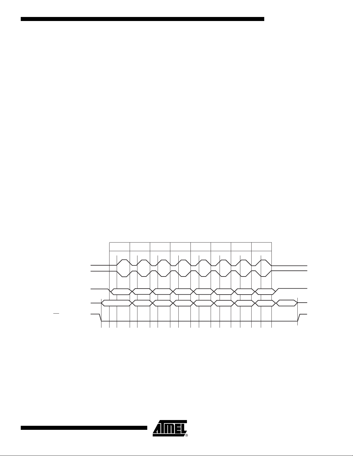
AT43USB355
SS Pin Functionality When the SPI is configured as a master (MSTR in SPCR is set), the user can determine the
direction of the SS pin. If SS is configured as an output, the pin is a general output pin which
does not affect the SPI system. If SS is configured as an input, it must be held high to ensure
Master SPI operation. If the SS pin is driven low by peripheral circuitry when the SPI is configured as master with the SS pin defined as an input, the SPI system interprets this as another
master selecting the SPI as a slave and starting to send data to it. To avoid bus contention, the
SPI system takes the following actions:
1. The MSTR bit in SPCR is cleared and the SPI system becomes a slave. As a result of
the SPI becoming a slave, the MOSI and SCK pins become inputs.
2. The SPIF flag in SPSR is set, and if the SPI interrupt is enabled and the I-bit in SREG
are set, the interrupt routine will be executed.
Thus, when interrupt-driven SPI transmittal is used in master mode, and there exists a possibility that SS is driven low, the interrupt should always check that the MSTR bit is still set.
Once the MSTR bit has been cleared by a slave select, it must be set by the user to re-enable
SPI master mode.
When the SPI is configured as a slave, the SS pin is always input. When SS is held low, the
SPI is activated and MISO becomes an output if configured so by the user. All other pins are
inputs. When SS is driven high, all pins are inputs, and the SPI is passive, which means that it
will not receive incoming data. Note that the SPI logic will be reset once the SS pin is brought
high. If the SS pin is brought high during a transmission, the SPI will stop sending and receiving immediately and both data received and data sent must be considered as lost.
Data Modes There are four combinations of SCK phase and polarity with respect to serial data, which are
determined by control bits CPHA and CPOL. The SPI data transfer formats are shown in Figure 20 and Figure 21.
Figure 20. SPI Transfer Format with CPHA = 0 and DORD = 0
SCK Cycle #
(For Reference)
SCK (CPOL = 0)
SCK (CPOL = 1)
MOSI
(From Master)
MISO
(From Slave)
SS (To Slave)
Note: * Not defined but normally LSB of character just received.
12345678
MSB
MSB
123456
LSB123456
LSB
*
2603G–USB–04/06
55
Page 56

Figure 21. SPI Transfer Format with CPHA = 1 and DORD = 0
SCK Cycle #
(For Reference)
SCK (CPOL = 0)
SCK (CPOL = 1)
MOSI
(From Master)
MISO
(From Slave)
SS (To Slave)
Note: * Not defined, but normally LSB of previously transmitted character.
12345678
MSB
MSB
*
LSB123456
123456
LSB
56
AT43USB355
2603G–USB–04/06
Page 57

AT43USB355
SPI Control Register – SPCR
Bit 7 6 5 4 3 2 1 0
$0D ($2D) SPIE SPE DORD MSTR CPOL CPHA SPR1 SPR0 SPCR
Read/Write R/W R/W R/W R/W R/W R/W R/W R/W
Initial Value 0 0 0 0 0 0 0 0
•Bit 7 – SPIE: SPI Interrupt Enable
This bit causes the SPI interrupt to be executed if SPIF bit in the SPSR register is set and the
global interrupts are enabled.
•Bit 6 – SPE: SPI Enable
When the SPE bit is set (one), the SPI is enabled. This bit must be set to enable any SPI
operations.
•Bit 5 – DORD: Data Order
When the DORD bit is set (one), the LSB of the data word is transmitted first.
When the DORD bit is cleared (zero), the MSB of the data word is transmitted first.
•Bit 4 – MSTR: Master/Slave Select
This bit selects Master SPI mode when set (one), and Slave SPI mode when cleared (zero). If
SS is configured as an input and is driven low while MSTR is set, MSTR will be cleared, and
SPIF in SPSR will become set. The user will then have to set MSTR to re-enable SPI master
mode.
•Bit 3 – CPOL: Clock Polarity
When this bit is set (one), SCK is high when idle. When CPOL is cleared (zero), SCK is low
when idle. Refer to Figure 20 and Figure 21 for additional information.
•Bit 2 – CPHA: Clock Phase
Refer to Figure 20 or Figure 21 for the functionality of this bit.
• Bits 1,0 – SPR1, SPR0: SPI Clock Rate Select 1 and 0
These two bits control the SCK rate of the device configured as a master. SPR1 and SPR0
have no effect on the slave. The relationship between SCK and the Oscillator Clock frequency
f
is shown in the following table:
CL
Table 20. Relationship Between SCK and the Oscillator Frequency
SPR1 SPR0 SCK Frequency
00 3 MHz
0 1 750 kHz
1 0 187.5 kHz
1 1 93.75 kHz
2603G–USB–04/06
57
Page 58

SPI Status Register – SPSR
Bit76543210
$0E ($2E) SPIF WCOL – – – – – – SPSR
Read/Write R R R R R R R R
Initial Value 0 0 0 0 0 0 0 0
•Bit 7 – SPIF: SPI Interrupt Flag
When a serial transfer is complete, the SPIF bit is set (one) and an interrupt is generated if
SPIE in SPCR is set (one) and global interrupts are enabled. If SS is an input and is driven low
when the SPI is in master mode, this will also set the SPIF flag. SPIF is cleared by the hardware when executing the corresponding interrupt handling vector. Alternatively, the SPIF bit is
cleared by first reading the SPI status register when SPIF is set (one), then accessing the SPI
Data Register (SPDR).
•Bit 6 – WCOL: Write Collision Flag
The WCOL bit is set if the SPI data register (SPDR) is written during a data transfer. The
WCOL bit (and the SPIF bit) are cleared (zero) by first reading the SPI Status Register when
WCOL is set (one), and then accessing the SPI Data Register.
• Bit 5..0 – Res: Reserved Bits
These bits are reserved bits in the AT43USB355 and will always read as zero.
SPI Data Register – SPDR
Bit 7 6 5 4 3 2 1 0
$0F ($2F) MSB – – – – – – LSB SPDR
Read/Write R/W R/W R/W R/W R/W R/W R/W R/W
Initial Value x x x x x x x x Undefined
The SPI Data Register is a read/write register used for data transfer between the register file
and the SPI Shift register. Writing to the register initiates data transmission. Reading the register causes the Shift Register Receive buffer to be read.
58
AT43USB355
2603G–USB–04/06
Page 59

AT43USB355
Analog-to-digital Converter
Feature list:
• 10-bit Resolution
• 4 LSB Integral Non-linearity
• ±2 LSB Absolute Accuracy
• 12 – 768 µs Conversion Time
• Up to 83 kSPS at Maximum Resolution
• 12 Multiplexed Input Channels
• Rail-to-rail Input Range
• Free Running or Single Conversion Mode
• Interrupt on ADC Conversion Complete
The AT43USB355 features a 10-bit successive approximation ADC. The ADC is connected to
a 12-channel Analog Multiplexer to pins AD0 – AD11. The ADC contains a Sample and Hold
Amplifier that ensures that the input voltage to the ADC is held at a constant level during conversion. A block diagram of the ADC is shown in Figure 22.
An external reference voltage must be applied to the V
range between 2.4V and the VCEXTA voltage.
Figure 22. Analog-to-digital Converter Block Schematic
ADC Conversion
Complete IRQ
pin. This voltage must be in the
REF
VREF
Analog
Inputs
8-bit Data Bus
MUX
12-Channel
ADC Multiplexer
Select (ADMUX)
10-bit DAC
-
+
Sample and Hold
Comparator
MUX2
MUX1
ADC Ctrl and Staus
Register (ADCSR)
MUX0
ADSC
ADEN
ADIF
ADIE
ADFR
ADIE
ADIF
Prescaler
Conversion Logic
ADPS1
ADPS2
15 0
ADC Data Register
(ADCH/ADCL)
ADPS0
ADC9..0
2603G–USB–04/06
59
Page 60

Operation The ADC converts an analog input voltage to a 10-bit digital value through successive approx-
imation. The minimum value represents V
on the V
pin minus one LSB. The analog input channel is selected by writing to the MUX
REF
and the maximum value represents the voltage
SSA
bits in ADMUX. Any of the twelve ADC input pins ADC11 – 0 can be selected as single-ended
inputs to the ADC.
The ADC can operate in two modes – Single Conversion and Free Running. In Single Conversion Mode, each conversion will have to be initiated by the user. In Free Running Mode, the
ADC is constantly sampling and updating the ADC Data Register. The ADFR bit in ADCSR
selects between the two available modes.
The ADC is enabled by setting the ADC Enable bit, ADEN in ADCSR. Input channel selections
will not go into effect until ADEN is set. The ADC does not consume power when ADEN is
cleared, so it is recommended to switch off the ADC before entering power-saving sleep
modes.
A conversion is started by writing a logical “1” to the ADC Start Conversion bit, ADSC. This bit
stays high as long as the conversion is in progress and will be set to zero by the hardware
when the conversion is completed. If a different data channel is selected while a conversion is
in progress, the ADC will finish the current conversion before performing the channel change.
The ADC generates a 10-bit result, which is presented in the ADC data register, ADCH and
ADCL. When reading data, ADCL must be read first, then ADCH, to ensure that the content of
the data register belongs to the same conversion. Once ADCL is read, ADC access to data
register is blocked. This means that if ADCL has been read and a conversion completes
before ADCH is read, neither register is updated and the result from the conversion is lost.
Then ADCH is read, ADC access to the ADCH and ADCL register is re enabled.
The ADC has its own interrupt that can be triggered when a conversion completes. When ADC
access to the data registers is prohibited between reading of ADCH and ADCL, the interrupt
will trigger even if the result is lost.
Figure 23. ADC Prescaler
ADEN
CK
ADPS0
ADPS1
ADPS2
Reset
CK4
CK/2
ADC Clock Source
7-bit ADC Prescaler
CK8
CK16
CK32
CK64
CK128
60
AT43USB355
2603G–USB–04/06
Page 61

AT43USB355
The successive approximation circuitry requires an input clock frequency between 15 kHz and
1 MHz to achieve maximum resolution. If a resolution of 10 bits is required, the input clock frequency to the ADC must be lower than 500 kHz to achieve a higher accuracy. See “ADC
Characteristics” on page 66 for more details. The ADC module contains a prescaler, which
divides the CK of 2 MHz clock input, to an acceptable ADC clock frequency.
The ADPS[0:2] bits in ADCSR are used to generate a proper ADC clock input frequency from
15.6 kHz to 1.0 MHz. The prescaler starts counting from the moment the ADC is switched on
by setting the ADEN bit in ADCSR. The prescaler keeps running for as long as the ADEN bit is
set and is continuously reset when ADEN is low.
When initiating a conversion by setting the ADSC bit in ADCSR, the conversion starts at the
following rising edge of the ADC clock cycle.
A normal conversion takes 12 ADC clock cycles. In certain situations, the ADC needs more
clock cycles for initialization and to minimize offset errors. Extended conversions take 25 ADC
clock cycles and occur as the first conversion after the ADC is switched on (ADEN in ADCSR
is set).
The actual sample-and-hold takes place 1.5 ADC clock cycles after the start of a conversion.
When a conversion is complete, the result is written to the ADC data registers and ADIF is set.
In Single Conversion Mode, ADSC is cleared simultaneously. The software may then set
ADSC again and a new conversion will be initiated on the first rising ADC clock edge. In Free
Running Mode, a new conversion will be started immediately after the conversion completes,
while ADSC remains high. Using Free Running Mode and an ADC clock frequency of 1 MHz
gives the lowest conversion time with a maximum resolution, 12 µs, equivalent to 83 kSPS.
For a summary of conversion times, see Table 21.
Figure 24. ADC Timing Diagram, Extended Conversion (Single Conversion Mode)
2603G–USB–04/06
61
Page 62

Figure 25. ADC Timing Diagram, Single Conversion
Figure 26. ADC Timing Diagram, Free Running Conversion
Table 21. ADC Conversion Time
Condition
Normal Conversion
62
AT43USB355
Sample and Hold (Cycles
from Start of Conversion) Conversion Time (Cycles) Conversion Time (µs)
12 10 12 - 768
2603G–USB–04/06
Page 63

AT43USB355
ADC Multiplexer Select Register – ADMUX
Bit 7 6 5 4 3 2 1 0
$08 ($28) – – – – MUX3 MUX2 MUX1 MUX0 ADMUX
Read/Write R R R R R/W R/W R/W R/W
Initial Value 0 0 N/A 0 0 0 0 0
• Bits 7..3 – Res: Reserved Bits
These bits are reserved bits in the AT43USB355 and always read as zero.
• Bits 3..0 – MUX3..MUX0: Analog Channel Select Bits 3-0
The value of these three bits selects which analog input ADC11..0 is connected to the ADC.
See Table 22 for details.
If these bits are changed during a conversion, the change will not go into effect until this conversion is complete (ADIF in ADCSR is set).
Table 22. Input Channel Selections
MUX3.0 Single-ended Input
0000 ADC0
0001 ADC1
0010 ADC2
0011 ADC3
0100 ADC4
0101 ADC5
0110 ADC6
0111 ADC7
1000 ADC8
1001 ADC9
1010 ADC10
1011 ADC11
11XX ADC0
2603G–USB–04/06
63
Page 64

ADC Control and Status Register – ADCSR
Bit76543210
$07 ($27) ADEN ADSC ADFR ADIF ADIE ADPS2 ADPS1 ADPS0 ADCSR
Read/Write R/W R/W R/W R/W R/W R/W R/W R/W
Initial Value 0 0 0 0 0 0 0 0
•Bit 7 – ADEN: ADC Enable
Writing a logical “1” to this bit enables the ADC. By clearing this bit to zero, the ADC is turned
off. Turning the ADC off while a conversion is in progress will terminate this conversion.
•Bit 6 – ADSC: ADC Start Conversion
In Single Conversion Mode, a logical “1” must be written to this bit to start each conversion. In
Free Running Mode, a logical “1” must be written to this bit to start the first conversion. The
first time ADSC has been written after the ADC has been enabled or if ADSC is written at the
same time as the ADC is enabled, an extended conversion will precede the initiated conversion. This extended conversion performs initialization of the ADC.
ADSC will read as one as long as a conversion is in progress. When the conversion is complete, it returns to zero. When a extended conversion precedes a real conversion, ADSC will
stay high until the real conversion completes. Writing a “0” to this bit has no effect.
•Bit 5 – ADFR: ADC Free Running Select
When this bit is set (one), the ADC operates in Free Running Mode. In this mode, the ADC
samples and updates the data registers continuously. Clearing this bit (zero) will terminate
Free Running Mode.
•Bit 4 – ADIF: ADC Interrupt Flag
This bit is set (one) when an ADC conversion completes and the data registers are updated.
The ADC Conversion Complete interrupt is executed if the ADIE bit and the I-bit in SREG are
set (one). ADIF is cleared by the hardware when executing the corresponding interrupt handling vector. Alternatively, ADIF is cleared by writing a logical “1” to the flag. Beware that if
doing a read-modify-write on ADCSR, a pending interrupt can be disabled. This also applies if
the SBI and CBI instructions are used.
•Bit 3 – ADIE: ADC Interrupt Enable
When this bit is set (one) and the I-bit in SREG is set (one), the ADC Conversion Complete
interrupt is activated.
• Bits 2..0 – ADPS2..ADPS0: ADC Prescaler Select Bits
These bits determine the division factor between the 2 MHz frequency and the input clock to
the ADC.
64
AT43USB355
2603G–USB–04/06
Page 65

AT43USB355
Table 23. ADC Prescaler Selections
ADPS2 ADPS1 ADPS0 Division Factor
0002
0012
0104
0118
10016
10132
11064
111128
ADC Data Register – ADCL and ADCH
Bit 7 6 5 4 3 2 1 0
$03 ($23) – – – – – – ADC9 ADC8 ADCH
$24 ($44) ADC7 ADC6 ADC5 ADC4 ADC3 ADC2 ADC1 ADC0 ADCL
Read/Write R R R R R R R R
Initial Value 0 0 0 0 0 0 0 0
Scanning Multiple Channels
When an ADC conversion is complete, the result is found in these two registers. In Free Run
Mode, it is essential that both registers are read, and that ADCL is read before ADCH.
Since change of analog channels is always delayed until a conversion is finished, the Free
Run Mode can be used to scan multiple channels without interrupting the converter. Typically,
the ADC Conversion Complete interrupt will be used to perform the channel shift. However,
the user should take the following fact into consideration:
The interrupt triggers once the result is ready to be read. In Free Run Mode, the next conversion will start immediately when the interrupt triggers. If ADMUX is changed after the interrupt
triggers, the next conversion has already started and the old setting is used.
2603G–USB–04/06
65
Page 66

ADC Characteristics
Symbol Parameter Condition Min Typ Max
Resolution 10 Bits
Unit
s
Integral Non-linearity V
Differential Non-linearity V
Zero Error (Offset) -2 2 LSB
Full Scale Error -4 4 LSB
V
REF
Reference Voltage 2.4 VCEXTA V
input resistance 25°C121824kΩ
V
REF
Analog Input Resistance 100 MΩ
Conversion Time 12 768 µs
Clock Frequency at 50% duty cycle 1 MHz
= VCEXTA 4 LSB
REF
= VCEXTA 4 LSB
REF
I/O-Ports All AVR ports have true Read-Modify-Write functionality when used as general digital I/O
ports. This means that the direction of one port pin can be changed without unintentionally
changing the direction of any other pin with the SBI and CBI instructions. The same applies for
changing drive value if configured as output or enabling/disabling of pull-up resistors if configured as input.
In the AT43USB355E, Port F[0:4] are used as the SPI signals for the external serial EEPROM.
Once the data from the SEEPROM are loaded to the SRAM, Port F[1:3] become available as
GPIO pins. Only cycling the power to the chip off and on again will temporarily assign these
pins as SEEPROM interface signals.
Port A Port A is an 8-bit bi-directional I/O port. The Port A output buffers can sink or source 2 mA.
Three I/O memory address locations are allocated for the Port A, one each for the Data Register PORTA, $1B($3B), Data Direction Register (DDRA), $1A($3A) and the Port A Input Pins
(PINA) $19($39). The Port A Input Pins address is read only, while the Data Register and the
Data Direction Register are read/write.
All port pins have individually selectable pull-up resistors. When pins PA0 to PA7 are used as
inputs and are externally pulled low, they will source current if the internal pull-up resistors are
activated.
66
AT43USB355
2603G–USB–04/06
Page 67

AT43USB355
Port A Data Register – PORTA
Bit 7 6 5 4 3 2 1 0
$1B ($3B) PORTA7 PORTA6 PORTA5 PORTA4 PORTA3 PORTA2 PORTA1 PORTA0 PORTA
Read/Write R/W R/W R/W R/W R/W R/W R/W R/W
Initial Value 0 0 0 0 0 0 0 0
Port A Data Direction Register – DDRA
Bit 7 6 5 4 3 2 1 0
$1A ($3A) DDA7 DDA6 DDA5 DDA4 DDA3 DDA2 DDA1 DDA0 DDRA
Read/Write R/W R/W R/W R/W R/W R/W R/W R/W
Initial Value 0 0 0 0 0 0 0 0
Port A Input Pins Address – PINA
Bit 7654 3 210
$19 ($39) PINA7 PINA6 PINA5 PINA4 PINA3 PINA2 PINA1 PINA0 PINA
Read/Write R R R R R R R R
Initial Value N/A N/A N/A N/A N/A N/A N/A N/A
PortA as General Digital I/O
The Port A Input Pins address (PINA) is not a register, and this address enables access to the
physical value on each Port A pin. When reading PORTA the Port A Data Latch is read, and
when reading PINA, the logical values present on the pins are read.
All 8 pins in Port A have equal functionality when used as digital I/O pins.
PAn, General I/O Pin: The DDAn bit in the DDRA register selects the direction of this pin, if
DDAn is set (one), PAn is configured as an output pin. If DDAn is cleared (zero), PAn is configured as an input pin. If PORTAn is set (one) when the pin is configured as an input pin, the
MOS pull-up resistor is activated. To switch the pull-up resistor off, the PORTAn has to be
cleared (zero) or the pin has to configured as an output pin. The Port A pins are tri-stated
when a reset condition becomes active, even if the clock is not active.
Table 24. DDAn Effects on Port A Pins
DDAn PORTAn I/O Comment
0 0 Input Tri-state (Hi-Z)
0 1 Input PAn will source current if ext. pulled low.
1 0 Output Push-Pull Zero Output
1 1 Output Push-Pull One Output
Note: n: 7,6...0, pin number.
2603G–USB–04/06
67
Page 68

Port B Port B is an 8-bit bi-directional I/O port. The Port B output buffers can sink or source 2 mA.
Three I/O memory address locations are allocated for the Port B, one each for the Data Register - PORTB, $18($38), Data Direction Register (DDRB), $17($37) and the Port B Input Pins
(PINB), $16($36). The Port B Input Pins address is read only, while the Data Register and the
Data Direction Register are read/write.
All port pins have individually selectable pull-up resistors. When pins PB0 to PB7 are used as
inputs and are externally pulled low, they will source current if the internal pull-up resistors are
activated
The Port B pins with alternate functions are shown in the following table:
Table 25. Port B Pins Alternate Functions
Port Pin Alternate Functions
PB0 T0 (Timer/Counter 0 External Counter Input)
PB1 T1 (Timer/Counter 1 External Counter Input)
PB4 SS (SPI Slave Select Input)
PB5 MOSI (SPI Bus Master Output/Slave Input)
PB6 MISO (SPI Bus Master Input/Slave Output)
PB7 SCK (SPI Bus Serial Clock)
When the pins are used for the alternate function the DDRB and PORTB register has to be set
according to the alternate function description.
68
AT43USB355
2603G–USB–04/06
Page 69
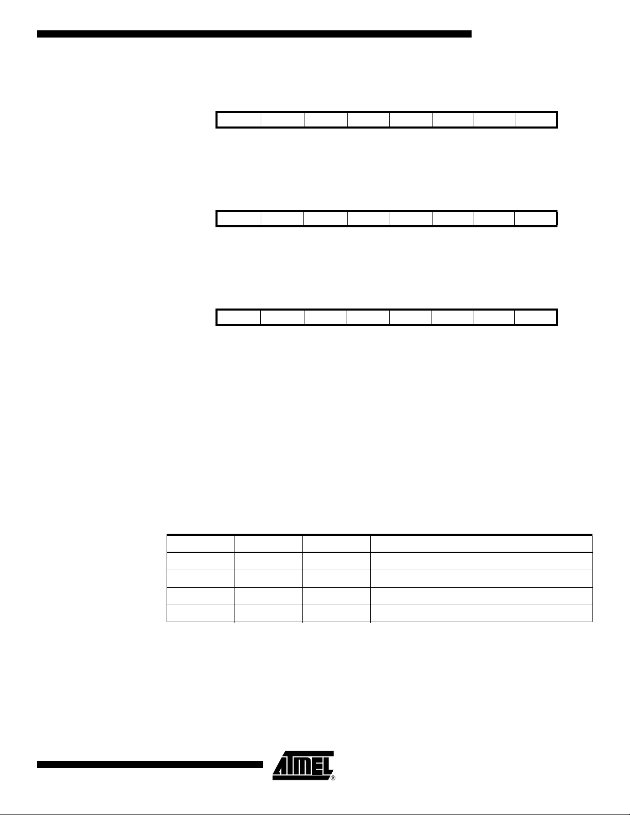
AT43USB355
Port B Data Register – PORTB
Bit 7 6 5 4 3 2 1 0
$18 ($38) PORTB7 PORTB6 PORTB5 PORTB4 PORTB3 PORTB2 PORTB1 PORTB0 PORTB
Read/Write R/W R/W R/W R/W R/W R/W R/W R/W
Initial Value 0 0 0 0 0 0 0 0
Port B Data Direction Register – DDRB
Bit 7 6 5 4 3 2 1 0
$17 ($37) DDB7 DDB6 DDB5 DDB4 DDB3 DDB2 DDB1 DDB0 DDRB
Read/Write R/W R/W R/W R/W R/W R/W R/W R/W
Initial Value 0 0 0 0 0 0 0 0
Port B Input Pins Address – PINB
Bit 7 6 5 4 3 2 1 0
$16 ($36) PINB7 PINB6 PINB5 PINB4 PINB3 PINB2 PINB1 PINB0 PINB
Read/Write R R R R R R R R
Initial Value N/A N/A N/A N/A N/A N/A N/A N/A
PortB as General Digital I/O
The Port B Input Pins address (PINB) is not a register, and this address enables access to the
physical value on each Port B pin. When reading PORTB, the Port B Data Latch is read, and
when reading PINB, the logical values present on the pins are read.
All 8 pins in port B have equal functionality when used as digital I/O pins.
PBn, General I/O Pin: The DDBn bit in the DDRB register selects the direction of this pin, if
DDBn is set (one), PBn is con-figured as an output pin. If DDBn is cleared (zero), PBn is configured as an input pin. If PORTBn is set (one) when the pin is configured as an input pin, the
MOS pull-up resistor is activated. To switch the pull-up resistor off, the PORTBn has to be
cleared (zero) or the pin has to configured as an output pin. The Port B pins are tri-stated
when a reset condition becomes active, even if the clock is not active.
Table 26. DDBn Effects on Port B Pins
DDBn PORTBn I/O Comment
0 0 Input Tri-state (Hi-Z)
0 1 Input PBn will source current if ext. pulled low.
1 0 Output Push-Pull Zero Output
1 1 Output Push-Pull One Output
Note: n: 7, 6...0, pin number.
2603G–USB–04/06
69
Page 70

Port D Port D is an 8-bit bi-directional I/O port. Its output buffers can sink or source 2 mA.
Three I/O memory address locations are allocated for the Port D, one each for the Data Register - PORTD, $12($32), Data Direction Register (DDRD), $11($31) and the Port D Input Pins
(PIND), $10($30). The Port D Input Pins address is read only, while the Data Register and the
Data Direction Register are read/write.
All port pins have individually selectable pull-up resistors. When pins PD0 to PD7 are used as
inputs and are externally pulled low, they will source current if the internal pull-up resistors are
activated
Some Port D pins have alternate functions as shown in Table 27.
Table 27. Port D Alternate Functions
Port Pin Alternate Function
PD2 INT0, External Interrupt 0
PD3 INT1, External Interrupt 1
PD5 OC1A Timer/Counter1 Output Compare A
PD6 OC1B Timer/Counter1 Output Compare B
When the pins are used for the alternate function the DDRD and PORTD register has to be set
according to the alternate function description.
Port D Data Register – PORTD
Bit 7 6 5 4 3 2 1 0
$12 ($32) PORTD7 PORTD6 PORTD5 PORTD4 PORTD3 PORTD2 PORTD1 PORTD0 PORTD
Read/Write R/W R/W R/W R/W R/W R/W R/W R/W
Initial Value 0 0 0 0 0 0 0 0
Port D Data Direction Register – DDRD
Bit 7654 3 210
$11 ($31) DDD7 DDD6 DDD5 DDD4 DDD3 DDD2 DDD1 DDD0 DDRD
Read/Write R/W R/W R/W R/W R/W R/W R/W R/W
Initial Value 0 0 0 0 0 0 0 0
Port D Input Pins Address – PIND
Bit 7 6 5 4 3 2 1 0
$10 ($30) PIND7 PIND6 PIND5 PIND4 PIND3 PIND2 PIND1 PIND0 PIND
Read/Write R R R R R R R R
Initial Value N/A N/A N/A N/A N/A N/A N/A N/A
The Port D Input Pins address (PIND) is not a register, and this address enables access to the
physical value on each Port D pin. When reading PORTD, the Port D Data Latch is read, and
when reading PIND, the logical values present on the pins are read.
70
AT43USB355
2603G–USB–04/06
Page 71

AT43USB355
PortD as General Digital I/O
PDn, General I/O Pin: The DDDn bit in the DDRD register selects the direction of this pin. If
DDDn is set (one), PDn is con-figured as an output pin. If DDDn is cleared (zero), PDn is configured as an input pin. If PORTDn is set (one) when the pin is configured as an input pin, the
MOS pull-up resistor is activated. To switch the pull-up resistor off, the PORTDn has to be
cleared (zero) or the pin has to configured as an output pin. The Port D pins are tri-stated
when a reset condition becomes active, even if the clock is not active.
Table 28. DDDn Bits on Port D Pins
DDDn PORTDn I/O Comment
0 0 Input Tri-state (Hi-Z)
0 1 Input PDn will source current if ext. pulled low.
1 0 Output Push-Pull Zero Output
1 1 Output Push-Pull One Output
Note: n: 7, 6...0, pin number.
2603G–USB–04/06
71
Page 72

Port F In the AT43USB355 Port F[1:3] is a 3-bit bi-directional I/O. Its output buffers can sink or source
2 mA Three I/O memory address locations are allocated for the Port F, one each for the Data
Register (PORTF), $06($26), Data Direction Register (DDRF), $05($25) and the Port F Input
Pins (PIND), $04($24). The Port F Input Pins address is read only, while the Data Register
and the Data Direction Register are read/write.
PF1 to PF3 pins have individually selectable pull-up resistors. When pins PPF1 to PF3 are
used as inputs and are externally pulled low, they will source current if the internal pull-up
resistors are activated.
In the SRAM version of the chip, the AT43USB355E, Port F is used for program memory
downloading immediately after power-on reset. After downloading is completed, PF0 is driven
high, while PF[1:3] becomes available as GPIO. In both versions of the chip, PF3 can be programmed as ICP, Timer/Counter 1 Input Capture.
Port F Data Register – PORTF
Bit 7 6 5 4 3 2 1 0
$06 ($26) – – – – PORTF3 PORTF2 PORTF1 – PORTF
Read/Write R R R R R/W R/W R/W R
Initial Value 0 0 0 0 0 0 0 0
Port F Data Direction Register – DDRF
Bit 7 6 5 4 3 2 1 0
$05 ($25) – – – – DDF3 DDF2 DDF1 – DDRF
Read/Write R R R R R/W R/W R/W R
Initial Value 0 0 0 0 0 0 0 0
Port F Input Pins Address – PINF
Bit 7 6 5 4 3 2 1 0
$04 ($24) – – – – PINF3 PINF2 PINF1 – PINF
Read/Write R R R R R R R R
Initial Value N/A N/A N/A N/A N/A N/A N/A N/A
The Port F Input Pins address (PINF) is not a register, and this address enables access to the
physical value on each Port F pin. When reading PORTF, the Port F Data Latch is read, and
when reading PINF, the logical values present on the pins are read.
72
AT43USB355
2603G–USB–04/06
Page 73

AT43USB355
PortF as General Digital I/O
PFn, General I/O Pin: In the AT43USB355E, after firmware downloading, the DDFn bit in the
DDRF register selects the direction of this pin. If DDFn is set (one), PFn is con-figured as an
output pin. If DDFn is cleared (zero), PFn is configured as an input pin. If PORTFn is set (one)
when the pin is configured as an input pin, the MOS pull-up resistor is activated. To switch the
pull-up resistor off, the PORTFn has to be cleared (zero) or the pin has to configured as an
output pin. The Port F pins are tri-stated when a reset condition becomes active, except PFO
of the AT43USB355E. This pin is dedicated as the slave select pin for the SEEPROM.
Table 29. DDFn Bits on Port F Pins
DDFn PORTFn I/O Comment
0 0 Input Tri-state (Hi-Z)
0 1 Input PFn will source current if ext. pulled low.
1 0 Output Push-Pull Zero Output
1 1 Output Push-Pull One Output
Note: n: 3, 2, 1, pin number.
2603G–USB–04/06
73
Page 74

Programming the USB Module
The USB hardware consists of two devices, hub and function, each with their own device
address and end-points. Its operation is controlled through a set of memory mapped registers.
The exact configuration of the USB device is defined by the software and it can be programmed to operate as a compound device, or as a hub only or as a function only. The hub
has the required control and interrupt end-points. The number of external downstream ports is
programmable as 1 or 2. The DP and DM pins of the unused port(s) must be connected to
ground. The USB function has one control end-point and 3 programmable end-points. All the
end-points have their own FIFO. Function end-points 1 and 2 FIFOs are 64 bytes deep and
function end-point 3 has an 8-byte FIFO. If the hub is disabled, one extra end-point becomes
available to the function.
The USB Function The USB function hardware is designed to operate in the single packet mode and to manage
the USB protocol layer. It consists of a Serial Interface Engine (SIE), end-point FIFOs and a
Function Interface Unit (FIU). The SIE performs the following tasks: USB signaling detection/generation, data serialization/de-serialization, data encoding/decoding, bit stuffing and unstuffing, clock/data separation, and CRC generation/checking. It also decodes and manages
all packet data types and packet fields.
The end-point FIFO buffers the data to be sent out or data received. The FIU manages the
flow of data between the SIE, FIFO and the internal microcontroller bus. It controls the FIFO
and monitors the status of the transactions and interfaces to the CPU. It initiates interrupts and
acts upon commands sent by the firmware.
The USB function hardware of the AT43USB355 makes the physical interface and the protocol layer transparent to the user. To start the process, the firmware must first enable the endpoints and which place them in receive mode by default. The device address by default is
address 0. The USB function hardware then waits for a SETUP token from the host. When a
valid the SETUP token is received, it automatically stores the DATA packet in end-point 0
FIFO and responds with an ACK. It then notifies the microcontroller through an interrupt. The
microcontroller reads the FIFO and parses the request.
Transactions for the non-control end-points are even simpler. Once the end-point is enabled, it
waits for an IN or an OUT token depending whether it is programmed as an IN or OUT endpoint. For example, if it is an IN end-point, the microcontroller simply loads the data into the
end-point's FIFO and sets a bit in the control and status register. The USB hardware will
assemble the data in a USB packet and waits for an IN token. When it receives one, it automatically responds by transmitting the DATA packet and completes the transaction by waiting
for the host's ACK. When one is received, the USB hardware will signal the microcontroller
that the transaction has been completed successfully. Retries and data toggles are performed
automatically by the USB hardware. When the IN end-point is not ready to send data, in the
case where the microcontroller has not filled the FIFO, it will automatically respond with a
NAK.
Similarly, an OUT end-point will wait for an OUT token. When one is received, it will store the
data in the FIFO, completes the transaction and interrupt the microcontroller, which then reads
the FIFO and enables the end-point for the next packet. If the FIFO is not cleared, the USB
hardware will responds with a NAK.
A detailed description of how USB transactions are handled is described in the following sections. First for a control end-point and then for non-control end-points.
74
AT43USB355
2603G–USB–04/06
Page 75

AT43USB355
Control Transfers at Control End-point EP0
The description given below is for the function control end-point, but applies to the hub control
end-point as well if the proper registers are used.
The following illustration describes the three possible types of control transfers – Control
Write, Control Read and No-data control:
Setup Data Status
Stage Stage Stage
Control
Write
Control
Read
SETUP(0) OUT(1) OUT(0) OUT(0/1)
DATA0 DATA1 DATA0 DATA0/1 DATA1(0)
SETUP(0)
DATA0 DATA1 DATA0 DATA0/1 DATA1(0)
IN(1) OUT(1)IN(0) IN(0/1)
…
IN(1)IN(1)
…
Setup Status
No-data
Control
Stage Stage
SETUP(0) IN(1)
DATA0 DATA1(0)
DATAn
DATA1(0)
Legend:
Data packet with PID’s
data toggle bit equal to n
Zero length DATA1 packet
The following state diagram shows how the various state transitions are triggered. Additional
decision making may take place within the response states to determine the next expected
state. Unmarked arcs represent transitions that trigger immediately following completion of the
response state processing. Stable states, those requiring an interrupt to exit having no
unmarked arcs as exit paths, are shown in bold.
RX_OUT_INT
TX_COMPLETE_INT
Control
Write Data
Response
Control
Write Status
Response
ANY STABLE STATE
(
RX_SETUP_INT
Setup
Response
RX_OUT_INT
TX_COMPLETE_INT
TX_COMPLETE_INT
Control
Read Status
Response
)
TX_COMPLETE_INT
Control
Read Data
Response
RX_OUT_INT
No-data
Status
Response
2603G–USB–04/06
Idle
75
Page 76

The following information describes how the AT43USB355’s USB hardware and firmware
operates during a control transfer between the host and the hub’s or function’s control endpoint.
Legend: DATA1/DATA0 = Data packet with DATA1 or DATA2 PID
DATA1(0) = Zero length DATA1 packet
Idle State This is the default state from power-up.
Setup Response State The Function Interface Unit (FIU) receives a SETUP token with 8 bytes of data from the Host.
The FIU stores the data in the FIFO, sends an ACK back to the host and asserts an
RX_SETUP interrupt.
Hardware Firmware
1. SETUP token, DATA from Host
2. ACK to Host
3. Store data in FIFO
4. Set RX SETUP → INT
5. Read UISR
6. Read CSR0
7. Read Byte Count
8. Read FIFO
9. Parse command data
10. Write to H/FCAR0:
a. If Control Read: set DIR, clear RX
SETUP, fill FIFO, set TX Packet
Ready in CAR0
b. If Control Write: clear DIR in CAR0
c. If no Data Stage: set Data End, clear
DIR, set Force STALL in CAR0
11. Set UIAR[EP0 INTACK] to clear the
interrupt source
76
AT43USB355
2603G–USB–04/06
Page 77

AT43USB355
No-data Status Response State
Control Read Data Response State
The Function Interface Unit receives an IN token from the Host. The FIU responds with a zero
length DATA1 packet until receiving an ACK from the host, then asserts a TX_COMPLETE
interrupt.
Hardware Firmware
1. IN token from Host
2. Send DATA1(0)
3. ACK from Host
4. Set TX COMPLETE → INT
5. Read UISR
6. Read CSR0
7. If SET ADDRESS, program the new
Address, set ADD_EN bit
8. Clear TX_COMPLETE, clear Data
End, set Force STALL in CAR0
9. Set UIAR[EP0 INTACK]
The Function Interface Unit receives an IN token from the Host. The FIU responds with NAKs
until TX_PACKET_READY is set. The FIU then sends the data in the FIFO upstream, retrying
until it successfully receives an ACK from the host. Finally, the FIU clears the
TX_PACKET_READY bit and asserts a TX_COMPLETE interrupt.
Hardware Firmware
1. IN token from Host
2. a. If TX Packet Ready = 1, send
DATA 0/ DATA 1
b. If TX Packet Ready = 0, send NAK
3. ACK from Host
4. Clear TX Packet Ready
Set TX Complete → INT
Repeat steps 1 through 8
5. Read UISR
6. Read CSR0
7. Clear TX COMPLETE in CAR0:
a. If more data: fill FIFO, set TX
Packet Ready, set DIR in CAR0
b. If no more data: set Force STALL,
set DATA END in CAR0
8. Set UIAR[EP0 INTACK] to clear
interrupt source
2603G–USB–04/06
77
Page 78

Control Read Status Response State
The Function Interface Unit receives an OUT token from the Host with a zero length DATA1
packet. The FIU responds with a NAK until TX_COMPLETE is cleared. The FIU will then ACK
the retried OUT token from the Host and assert an RX_OUT interrupt.
Hardware Firmware
1. OUT token from Host
2. DATA1(0) from Host
3. TX Complete = 0 ?
a. If yes, ACK to Host
Set RX OUT → INT
b. If no, NAK to Host
4. Read UISR
5. Read CSR0
6. Clear RX OUT, set Data End, set
Force Stall in H/FCAR0.
Note: A SETUP token will clear Data
End, therefore, it is not cleared by
FW in case Host retries.
7. Set UIAR[EP0 INTACK] to clear
interrupt source
Control Write Data Response State
The Function Interface Unit receives an OUT token from the Host with a DATA packet. The
FIU places the incoming data into the FIFO, issues an ACK to the host, and asserts an
RX_OUT interrupt.
Hardware Firmware
1. OUT token from Host
2. Put DATA0/DATA1 into FIFO
3. ACK to Host
4. Set RX OUT → INT
5. Read UISR
6. Read CSR0
7. Read FIFO
8. Clear RX OUT
If last data packet, set Force STALL,
set DATA END.
9. Set UIAR[EP0 INTACK] to clear the
interrupt source
Repeat steps 1 through 9 until last DATA PACKET:
78
AT43USB355
2603G–USB–04/06
Page 79

AT43USB355
Control Write Status Response State
The Function Interface Unit receives an IN token from the Host. The FIU responds with a zero
length DATA1 packet, retrying until it receives an ACK back from the Host. The FIU then
asserts a TX_COMPLETE interrupt.
Hardware Firmware
1. IN token from Host
2. Send DATA1(0)
3. ACK from Host
4. Set TX Complete → INT
5. Read UISR
6. Read CSR0
7. Clear TX COMPLETE, clear Data
End, set Force STALL in CAR0
8. Set UIAR[EP0 INTACK] to clear the
interrupt source
2603G–USB–04/06
79
Page 80

Interrupt/Bulk IN Transfers at Function End-point
The firmware must first condition the end-point through the End-point Control Register, FENDP1/2/3_CNTR:
Set end-point direction: set EPDIR
Set interrupt or bulk: EPTYPE = 11 or 10
Enable end-point: set EPEN
The Function Interface Unit receives an IN token from the Host. The FIU responds with NAKs
until TX_PACKET_READY is set. The FIU then sends the data in the FIFO upstream, retrying
until it successfully receives an ACK from the host. Finally, the FIU clears the
TX_PACKET_READY bit and asserts a TX_COMPLETE interrupt.
1. Read UISR
2. Read FCSR1/2/3
3. Clear TX_COMPLETE
If more data: fill FIFO, set TX Packet Ready
Wait for TX_COMPLETE interrupt
If no more data: set DATA END in FCAR1/2/3
4. Set UIAR[FEP1/2/3 INTACK] to clear the interrupt source
Interrupt/Bulk OUT Transfers at Function End-point EP1, 2 and 3
The firmware must first condition the end-point through the End-point Control Register, FENDP1/2/3_CNTR:
Set end-point direction: clear EPDIR
Set interrupt or bulk: EPTYPE = 11 or 10
Enable end-point: set EPEN
The Function Interface Unit receives an OUT token from the Host with a DATA packet. The
FIU places the incoming data into the FIFO, issues an ACK to the host, and asserts an
RX_OUT interrupt.
1. Read UISR
2. Read FCSR1/2/3
3. Read FIFO
4. Clear RX_OUT
If more data:
Wait for RX_OUT interrupt
If no more data: set DATA END
5. Set UIAR[FEP1/2/3 INTACK] to clear the interrupt source
80
AT43USB355
2603G–USB–04/06
Page 81

AT43USB355
USB Registers The following sections describe the registers of the AT43USB355’s USB hub and function
units.
Reading a bit for which the microcontroller does not have read access will yield a zero value
result. Writing to a bit for which the microcontroller does not have write access has no effect.
Hub Address Register
– HADDR
The USB hub contains an address register that contains the hub address assigned by the
host. This Hub Address Register must be programmed by the microcontroller once it has
received a SET_ADDRESS request from the host. The USB hardware uses the new address
only after the status phase of the transaction is completed when the microcontroller has
enabled the new address by setting bit 0 of the Global State Register. After power-up or reset,
this register will contain the value of 0x00.
Hub Address Register – HADDR
Bit 7 6 5 4 3 2 1 0
$1FEF SAEN HADD6 HADD5 HADD4 HADD3 HADD2 HADD1 HADD0 HADDR
Read/Write R/W R/W R/W R/W R/W R/W R/W R/W
Initial Value 0 0 0 0 0 0 0 0
• Bit 7 – SAEN: Single Address Enable
The Single Address Enable bit allows the microcontroller to configure the AT43USB355 into a
single address or a composite device. Once this capability is enabled, the hub end-point 0
(HEP0) is converted from a control end-point to a programmable function end-point FEP3; all
the end-points would then operate on the single address.
• Bit 6..0 – HADD6...0: Hub Address[6:0]
2603G–USB–04/06
81
Page 82

Function Address
Register – FADDR
End-point Registers
The USB function contains an address register that contains the function address assigned by
the host. This Function Address Register must be programmed by the microcontroller once it
has received a SET_ADDRESS request from the host and completed the status phase of the
transaction. After power up or reset, this register will contain the value of 0x00.
Function Address Register – FADDR
Bit76543210
$1FEE FEN FADD6 FADD5 FADD4 FADD3 FADD2 FADD1 FADD0 FADDR
Read/Write R/W R/W R/W R/W R/W R/W R/W R/W
Initial Value 0 0 0 0 0 0 0 0
• Bit 7 – FEN: Function Enable
The Function Enable bit (FEN) allows the firmware to enable or disable the function endpoints. The firmware will set this bit after receipt of a reset through the hub, SetPortFeature[PORT_RESET]. Once this bit is set, the USB hardware passes to and from the host.
When the Single Address bit is set, the condition of FEN is ignored.
• Bit 6..0 – FADD6...0: Function Address[6:0]
Hub End-point 0 Control Register – HEND-P0_CR
Function End-point 0 Control Register – FEND-P0_CR
Bit 765432 1 0
$1FE7 EPEN – – – DTGLE EPDIR EPTYPE1 EPTYPE0
$24 ($44) EPEN – – – DTGLE EPDIR EPTYPE1 EPTYPE0 FEND-P0_CR
Read/Write R/W R R R R/W R/W R/W R/W
Initial Value 0 0 0 0 0 0 0 0
HENDP0_CR
• Bit 7 – EPEN: End-point Enable
0 = Disable end-point
1 = Enable end-point
• Bit 6..4 – Reserved
These bits are reserved in the AT43USB355 and will read as zero.
• Bit 3 – DTGLE: Data Toggle
Identifies DATA0 or DATA1 packets. This bit will automatically toggle and requires clearing by
the firmware only in certain special circumstances.
• Bit 2 – EPDIR: End-point Direction
0 = Out
1 = In
• Bit 1, 0 – EPTYPE: End-point Type
82
These bits must be programmed as 0, 0.
AT43USB355
2603G–USB–04/06
Page 83
AT43USB355
Function End-point 1..3 Control Register – FEND-P1..3_CR
Bit 7 6 5 4 3 2 1 0
$1FE4 EPEN – – – DTGLE EPDIR EPTYPE1 EPTYPE0
$1FE3 EPEN – – – DTGLE EPDIR EPTYPE1 EPTYPE0
$1FE2 DTGLE EPDIR EPTYPE1 EPTYPE0
Read/Write R/W R R R R/W R/W R/W R/W
Initial Value 0 0 0 0 0 0 0 0
• Bit 7 – EPEN: End-point Enable
0 = Disable end-point
1 = Enable end-point
• Bit 6..4 – Reserved
These bits are reserved in the AT43USB355 and will read as zero.
• Bit 3 – DTGLE: Data Toggle
FENDP1_CR
FENDP2_CR
FENDP3_CR
Identifies DATA0 or DATA1 packets. This bit will automatically toggle and requires clearing by
the firmware only in certain special circumstances.
• Bit 2 – EPDIR: End-point Direction
0 = Out
1 = In
• Bit 1, 0 – EPTYPE: End-point Type
These bits programs the type of end-point.
Bit1 Bit0 Type
0 1 Isochronous
10Bulk
1 1 Interrupt
2603G–USB–04/06
83
Page 84

Hub End-point 0 Data Register – HDR0
Function End-point 0..3 Data Register – FDR0..3
Bit 7 6 5 4 3 2 1 0
$1FD7 DATA7 DATA6 DATA5 DATA4 DATA3 DATA2 DATA1 DATA0 HDR0
$1FD5 DATA7 DATA6 DATA5 DATA4 DATA3 DATA2 DATA1 DATA0 FDR0
$1FD4 DATA7 DATA6 DATA5 DATA4 DATA3 DATA2 DATA1 DATA0 FDR1
$1FD3 DATA7 DATA6 DATA5 DATA4 DATA3 DATA2 DATA1 DATA0 FDR2
$1FD2 DATA7 DATA6 DATA5 DATA4 DATA3 DATA2 DATA1 DATA0 FDR3
Read/Write R/W R/W R/W R/W R/W R/W R/W R/W
Initial Value 0 0 0 0 0 0 0 0
This register is used to read data from or to write data to the Hub End-point 0 FIFO.
• Bit 7..0 – FDAT7..0: FIFO Data
Hub end-point 1 has a single byte data register instead of a FIFO. This data register contains
the hub and port status change bitmap. This data register is automatically updated by the USB
hardware and is not accessible by the firmware. The bits in this register when read by the host
will be:
Bit 7 6 5 4 3 2 1 0
$ – – – – P3 SC P2 SC P1 SC H SC HDR1
Read/Write R/W R/W R/W R/W R/W R/W R/W R/W
Initial Value 0 0 0 0 0 0 0 0
• Bit 7...4 – Reserved
These bits are reserved in the AT43USB355 and will read as zero.
• Bit 3 – P3 SC: Port 3 Status Change
• Bit 2 – P2 SC: Port 2 Status Change
• Bit 1 – P1 SC: Port 1 Status Change
• Bit 0 – H SC: Hub Status Change
84
AT43USB355
2603G–USB–04/06
Page 85
AT43USB355
Hub End-point 0 Byte Count Register – HBYTE_CNT0
Function End-point 0..3 Byte Count Register – FBYTE_CNT0..3
The contents of these registers stores the number of bytes to be sent or that was received by
USB Hub and Function end-points. This count includes the 16-bit CRC. To get the actual byte
count of the data, subtract the count in the register by 2. The hub EP0 and function EP3 have
8 byte FIFOs while function EP1 and EP2 have 64 byte FIFOs. Hub end-point 1 has no byte
count register.
Bit 76543 210
Hub EP0 $1FCF – – BYTCT5 BYTCT4 BYTCT3 BYTCT2 BYTCT1 BYTCT0 HBYTE_CNT0
Function EP0 $1FCD – – BYTCT5 BYTCT4 BYTCT3 BYTCT2 BYTCT1 BYTCT0 FBYTE_CNT0
Function EP1 $1FCC – BYTCT6 BYTCT5 BYTCT4 BYTCT3 BYTCT2 BYTCT1 BYTCT0 FBYTE_CNT1
Function EP2 $1FCB – BYTCT6 BYTCT5 BYTCT4 BYTCT3 BYTCT2 BYTCT1 BYTCT0 FBYTE_CNT2
Function EP3 $1FCA – – BYTCT5 BYTCT4 BYTCT3 BYTCT2 BYTCT1 BYTCT0 FBYTE_CNT3
Read/Write R R R R/W R/W R/W R/W R/W
Initial Value 0 0 0 0 0 0 0 0
• Bit 7..6 – Reserved
These bits are reserved in the AT43USB355 and will read as zero.
• Bit 5..0 – BYTCT5..0: Byte Count – Length of End-point Data Packet
2603G–USB–04/06
85
Page 86

Hub End-point 0 Service Routine Register – HCSR0
Function End-point 0 Service Routine Register – FCSR0
Bit 7 6 5 4 3 2 1 0
Function EP0 $1FDF – – – – STALL SENT RX SETUP RX OUT PACKET TX COMPLETE HCSR0
Function EP0 $1FDD – – – – STALL SENT RX SETUP RX OUT PACKET TX COMPLETE FCSR0
Read/Write R R R R R R R R
Initial Value 0 0 0 0 0 0 0 0
• Bit 7..4 – Reserved
These bits are reserved in the AT43USB355 and will read as zero.
• Bit 3 – STALL SENT
The USB hardware sets this bit after a STALL has been sent to the host. The firmware uses
this bit when responding to a Get Status[End-point] request. It is a read only bit and that is
cleared indirectly by writing a one to the STALL_SENT_ACK bit of the Control and Acknowledge Register.
• Bit 2 – RX SETUP: Setup Packet Received
This bit is used by control end-points only to signal to the microcontroller that the USB hardware has received a valid SETUP packet and that the data portion of the packet is stored in
the FIFO. The hardware will clear all other bits in this register while setting RX SETUP. If interrupt is enabled, the microcontroller will be interrupted when RX SETUP is set. After the
completion of reading the data from the FIFO, firmware should clear this bit by writing a one to
the RX_SETUP_ACK bit of the Control and Acknowledge Register.
• Bit 1 – RX OUT PACKET
The USB hardware sets this bit after it has stored the data of an OUT transaction in the FIFO.
While this bit is set, the hardware will NAK all OUT tokens. The USB hardware will not overwrite the data in the FIFO except for an early set-up. RX OUT Packet is used for the following
operations:
1. Control write transactions by a control end-point.
2. OUT transaction with DATA1 PID to complete the status phase of a control end-point.
Setting this bit causes an interrupt to the microcontroller if the interrupt is enabled. FW clears
this bit after the FIFO contents have been read by writing a one to the
RX_OUT_PACKET_ACK bit of the Control and Acknowledge Register.
• Bit 0 – TX COMPL: Transmit Completed
This bit is used by a control end-point hardware to signal to the microcontroller that it has successfully completed certain transactions. TX Complete is set at the completion of a:
1. Control read data stage.
2. Status stage without data stage.
3. Status stage after a control write transaction.
This bit is read only and is cleared indirectly by writing a one to the TX_COMPLETE_ACK bit
of the Control and Acknowledge Register.
86
AT43USB355
2603G–USB–04/06
Page 87

AT43USB355
Hub End-point 0 Control and Acknowledge Register – HCAR0
Function End-point 0 Control and Acknowledge Register – FCAR0
Bit 7 6 5 4 3 2 1 0
Hub EP0
$1FA7
Function
EP0 $1FDD
Read/Write R/W R/W R/W R/W R/W R/W R/W R/W
Initial Value 0 0 0 0 0 0 0 0
DIR
DIR
DATA
END
DATA
END
FORCE
STALL
FORCE
STALL
TX
PACKET
READY
TX
PACKET
READY
•Bit 7 – DIR: Control transfer direction
It is set by the microcontroller firmware to indicate the direction of a control transfer to the USB
hardware. The FW writes to this bit location after it receives an RX SETUP interrupt. The hardware uses this bit to determine the status phase of a control transfer.
0 = control write or no data stage
1 = control read
•Bit 6 – DATA END
STALL_
SENT_
ACK
STALL_
SENT_
ACK
RX_
SETUP_
ACK
RX_
SETUP_
ACK
RX_OUT_
PACKET_
ACK
RX_OUT_
PACKET_
ACK
TX_
COMPLETE_
ACK
TX_
COMPLETE_
ACK
HCAR0
FCAR0
When set to 1 by firmware, this bit indicate that the microcontroller has either placed the last
data packet in FIFO, or that the microcontroller has processed the last data packet it expects
from the Host. This bit is used by control end-points only together with bit 4 (TX Packet Ready)
to signal the USB hardware to go to the STATUS phase after the packet currently residing in
the FIFO is transmitted. After the hardware completes the STATUS phase it will interrupt the
microcontroller without clearing this bit.
•Bit 5 – FORCE STALL
This bit is set by the microcontroller to indicate a stalled end-point. The hardware will send a
STALL handshake as a response to the next IN or OUT token, or whenever there is a control
transfer without a Data Stage.
The microcontroller sets this bit if it wants to force a STALL. A STALL is sent if any of the following condition is encountered:
1. An unsupported request is received.
2. The host continues to ask for data after the data is exhausted.
3. The control transfer has no data stage.
•Bit 4 – TX PACKET READY: Transmit Packet Ready
When set by the firmware, this bit indicates that the microcontroller has loaded the FIFO with a
packet of data. This bit is cleared by the hardware after the USB Host acknowledges the
packet. For ISO end-points, this bit is cleared unconditionally after the data is sent.
This bit is used for the following operations:
1. Control read transactions by a control end-point.
2. IN transactions with DATA1 PID to complete the status phase for a control end-point,
when this bit is zero but Data End set high (bit 4).
3. By a BULK IN or ISO IN or INT IN end-point.
2603G–USB–04/06
The microcontroller should write into the FIFO only if this bit is cleared. After it has completed
writing the data, it should set this bit. This data can be of zero length.
87
Page 88

Hardware clears this bit after it receives an ACK. If the interrupt is enabled and if the TX Complete bit is set, clearing the TX Packet Ready bit by the hardware causes an interrupt to the
microcontroller.
•Bit 3 – STALL_SENT_ACK: Acknowledge Stall Sent Interrupt
Firmware sets this bit to clear STALL SENT, CSR bit 3. The 1 written in the CSRACK3 bit is
not actually stored and thus does not have to be cleared.
•Bit 2 – RX_SETUP_ACK: Acknowledge RX SETUP Interrupt
Firmware sets this bit to clear RX SETUP, CSR bit2. The 1 written in the CSRACK2 bit is not
actually stored and thus does not have to be cleared.
•Bit 1 – RX_OUT_PACKET_ACK: Acknowledge RX OUT PACKET Interrupt
Firmware sets this bit to clear RX OUT PACKET, CSR bit1. The 1 written in the CSRACK1 bit
is not actually stored and thus does not have to be cleared.
•Bit 0 – TX_COMPLETE_ACK: Acknowledge TX COMPLETE Interrupt
Firmware sets this bit to clear TX COMPLETE, CSR bit0. The 1 written in the CSRACK0 bit is
not actually stored and thus does not have to be cleared.
Function End-point 0..3 Service Routine Register – FCSR0..3
Bit 7654 3 2 1 0
Function EP1 $1FDC – – – – STALL SENT – RX OUT PACKET TX COMPLETE FCSR1
Function EP2 $1FDB – – – – STALL SENT – RX OUT PACKET TX COMPLETE FCSR2
Function EP3 $1FDA – – – – STALL SENT – RX OUT PACKET TX COMPLETE FCSR3
Read/Write R R R R R R R R
Initial Value 0 0 0 0 0 0 0 0
• Bit 7..4 – Reserved
These bits are reserved in the AT43USB355 and will read as zero.
• Bit 3 – STALL SENT
The USB hardware sets this bit after a STALL has been sent to the host. The firmware uses
this bit when responding to a Get Status[End-point] request. It is a read only bit and that is
cleared indirectly by writing a one to the STALL_SENT_ACK bit of the Control and Acknowledge Register.
• Bit 2 – Reserved
This bit is reserved in the AT43USB355 and will read as zero.
• Bit 1 – RX OUT PACKET
The USB hardware sets this bit after it has stored the data of an OUT transaction in the FIFO.
While this bit is set, the hardware will NAK all OUT tokens. The USB hardware will not overwrite the data in the FIFO except for an early set-up. RX OUT Packet is used by a BULK OUT
or ISO OUT or INT OUT end-point.
Setting this bit causes an interrupt to the microcontroller if the interrupt is enabled. FW clears
this bit after the FIFO contents have been read by writing a one to the RX_SETUP_ACK bit of
the Control and Acknowledge Register.
• Bit 0 – TX COMPLETE: Transmit Completed
This bit is used by the end-point hardware to signal to the microcontroller that the IN transaction was completed successfully. This bit is read only and is cleared indirectly by writing a one
to the TX_COMPLETE_ACK bit of the Control and Acknowledge Register.
88
AT43USB355
2603G–USB–04/06
Page 89

AT43USB355
Function End-point 0..3 Control and Acknowledge Register – FCAR0..3
Bit 7 6 5 4 3 2 1 0
DATA
Function EP1 $1FA4 –
Function EP2 $1FA3 –
Function EP3 $1FA2 –
Read/Write R R/W R/W R/W R/W R R/W R/W
Initial Value 0 0 0 0 0 0 0 0
END
DATA
END
DATA
END
FORCE
STALL
FORCE
STALL
FORCE
STALL
• Bit 7 – Reserved
This bit is reserved in the AT43USB355 and will read as zero.
• Bit 6 – DATA END
When set to 1 by firmware, this bit indicate that the microcontroller has either placed the last
data packet in FIFO, or that the microcontroller has processed the last data packet it expects
from the Host.
• Bit 5 – FORCE STALL
This bit is set by the microcontroller to indicate a stalled end-point. The hardware will send a
STALL handshake as a response to the next IN or OUT token. The microcontroller sets this bit
if it wants to force a STALL. A STALL is send if the host continues to ask for data after the data
is exhausted.
• Bit 4 – TX PACKET RDY: Transmit Packet Ready
TX PACKET
RDY
TX PACKET
RDY
TX PACKET
RDY
STALL_SENT-
ACK
STALL_SENT-
ACK
STALL_SENT-
ACK
–
–
–
RX_OUT_PACKET
_ACK
RX_OUT_PACKET
_ACK
RX_OUT_PACKET
_ACK
TX_COMPLETE
_ACK
TX_COMPLETE
-ACK
TX_COMPLETE
-ACK
FCAR1
FCAR2
FCAR3
When set by the firmware, this bit indicates that the microcontroller has loaded the FIFO with a
packet of data. This bit is cleared by the hardware after the USB Host acknowledges the
packet. For ISO end-points, this bit is cleared unconditionally after the data is sent.
The microcontroller should write into the FIFO only if this bit is cleared. After it has completed
writing the data, it should set this bit. This data can be of zero length.
The hardware clears this bit after it receives an ACK. If the interrupt is enabled and if the TX
Complete bit is set, clearing the TX Packet Ready bit by the hardware causes an interrupt to
the microcontroller.
• Bit 3 – STALL_SENT_ACK: Acknowledge Stall Sent Interrupt
Firmware sets this bit to clear STALL SENT, CSR bit 3. The 1 written in the CSRACK3 bit is
not actually stored and thus does not have to be cleared.
• Bit 2 – Reserved
This bit is reserved in the AT43USB355 and will read as zero.
• Bit 1 – RX_OUT_PACKET_ACK: Acknowledge RX OUT PACKET Interrupt
Firmware sets this bit to clear RX OUT PACKET, CSR bit1. The 1 written in the CSRACK1 bit
is not actually stored and thus does not have to be cleared.
• Bit 0 – TX_COMPLETE_ACK: Acknowledge TX COMPLETE Interrupt
Firmware sets this bit to clear TX COMPLETE, CSR bit0. The 1 written in the CSRACK0 bit is
not actually stored and thus does not have to be cleared.
2603G–USB–04/06
89
Page 90

USB Hub The hub in a USB system provides for the electrical interface between USB devices and the
host. The major functions that the hub must supports are:
• Connectivity
• Power management
• Device connect and disconnect
• Bus fault detection and recovery
• Full speed and low speed device support
A hub consists of two major components: a hub repeater and a hub controller. The hub
repeater is responsible for:
• Providing upstream connectivity between the selected device and the Host
• Managing connectivity setup and tear-down
• Handling bus fault detection and recovery
• Detecting connect/disconnect on each port
The Hub Controller is responsible for:
• Hub enumeration
• Providing configuration information to the host
• Providing status of each port to the host
• Controlling each port per host command
The first two tasks of the Hub Controller are similar to that of a USB function and will not be
described in detail in the following section. The descriptions will cover the features of the
AT43USB355's hub and how to program it to make a USB-compliant hub.
Control transactions for the Hub Control End-point proceed exactly the same way as those
described for the embedded function. The operation of the hub's End-point 1 is fully implemented in the hardware and does not need any firmware support. Any status changes within
the Hub will automatically update Hub End-point 1, which will be sent to the host at the next IN
token that is addressed to it. If no change has occurred, the interrupt end-point will respond
with a NAK.
90
AT43USB355
2603G–USB–04/06
Page 91

Hub General Registers Global State Register – GLB_STATE
Bit 7 6 5 4 3 2 1 0
$1FFB – – – SUSP FLG RESUME FLG RMWUPE CONFG HADD EN GLB_STATE
Read/Write R R R R R R/W R/W R/W
Initial Value 0 0 0 0 0 0 0 0
• Bit 7...5 – Reserved Bits
These bits are reserved in the AT43USB355 and will read as zeros.
•Bit 4 – SUSP FLG: Suspend Flag
This bit is set to 1 while the USB hardware is in the suspended state. This bit is a firmware
read only bit. It is set and cleared by the USB hardware.
•Bit 3 – RESUME FLGL Resume Flag
When the USB hardware receives a resume signal from the upstream device it sets this bit.
This bit will stay set until the USB hardware completes the downstream resume signaling. This
bit is a firmware read only bit. It is set and cleared by the USB hardware.
•Bit 2 – RMWUPE: Remote Wakeup Enable
This bit is set if the host enables the hub's remote wakeup feature.
•Bit 1 – CONFG: Configured
AT43USB355
This bit is set by firmware after a valid SET_CONFIGURATION request is received. It is
cleared by a reset or by a SET_CONFIGURATION with a value of 0.
•Bit 0 – HADD EN: Hub Address Enabled
This bit is set by firmware after the status phase of a SET_ADDRESS request transaction so
the hub will use the new address starting at the next transaction.
2603G–USB–04/06
91
Page 92

Hub Status Register In the AT43USB355 overcurrent detection and port power switch control output processing is
done in firmware. The hardware is designed so that various types of hubs are possible just
through firmware modifications.
1. Hub local power status, bits 0 and 2, are optional features and apply to hubs that report
on a global basis. If this feature is not used, both these bits should be programmed to
0. To use this feature, the firmware needs to know the status of the local power supply,
which requires an input pin and extra internal or external circuitry.
2. Hub overcurrent status, bits 1 and 3, apply to self powered hubs with bus powered SIE
only, or hubs that are programmable as self/bus powered. The firmware should clear
these two bits to 0.
The firmware uses bits 1 and 3 to generate bit 0 of the Hub and Port Status Change Bitmap
which is transmitted through the Hub End-point1 Data Register. Bit 0 of this register is a 1
whenever bit 1 or 3 of HSTATR is a 1.
Hub Status Register – HSTR
Bit76543210
$1FC7 – – – – OVLSC L PS C OVI LPS HSTR
Read/Write R R R R R/W R/W R/W R/W
Initial Value 0 0 0 0 0 0 0 0
• Bit 7..4 – Reserved
These bits are reserved in the AT43USB355 and will read as zero.
• Bit 3 – OVLSC: Overcurrent Status Change
0 = No change has occurred on Overcurrent Indicator
1 = Overcurrent Indicator has changed
• Bit 2 – LPSC: Hub Local Power Status Change
0 = No change has occurred on Local Power Status
1 = Local Power Status has changed
• Bit 1 – OVI: Overcurrent Indicator
0 = All power operations normal
1 = An overcurrent exist on a hub wide basis
• Bit 0 – LPS: Hub Local Power Status
0 = Local power supply is good
1 = Local power supply is lost (inactive)
92
AT43USB355
2603G–USB–04/06
Page 93

AT43USB355
Hub Port Control Register – HPCON
Bit76543210
$1FC5 – HPCON2 HPCON1 HPCON0 – HPADD2 HPADD1 HPADD0 HPCON
Read/Write R R/W R/W R/W R R/W R/W R/W
Initial Value 0 0 0 0 0 0 0 0
•Bit 7 – Reserved
This bits is reserved in the AT43USB355 and will read as zero.
• Bit 6..4 – HPCON2..0: Hub Port Control Command
These bits are written by firmware to control the port states upon receipt of a Host request.
Bit6 Bit5 Bit4 Action
000Disable port
0 0 1 Enable port
0 1 0 Reset and enable port
0 1 1 Suspend port
1 0 0 Resume port
Disable Port = ClearPortFeature(PORT_ENABLE)
Action: USB hardware places addressed port in disabled state. Port 1 is placed in disabled
state by firmware.
Enable Port = SetPort Feature(PORT_ENABLE)
Action: USB hardware places addressed port in enabled state. Firmware is responsible for
placing Port 1 in enabled state.
Reset and Enable Port = SetPort Feature(PORT_RESET)
Action: USB hardware drives reset signaling through addressed port. USB hardware and
firmware resets their embedded function registers to the default state.
Suspend Port = SetPortFeature(PORT_SUSPEND)
Action: USB hardware places port in idle state and stops propagating traffic through the
addressed port. Firmware places Port 1 in suspend state by disabling its end-points and placing the peripheral function in its low power state.
Resume Port = ClearPortFeature(PORT_SUSPEND)
Action: USB hardware sends resume signaling to addressed port and then enables port.
Firmware takes the embedded function out of the suspend state and enables Port 1's endpoints.
•Bit 3 – Reserved
This bits is reserved in the AT43USB355 and will read as zero.
• Bit 2..0 – HPCON2..0: Hub Port Address
2603G–USB–04/06
93
Page 94

These bits define which port is being addressed for the command defined by bits [2:0].
Bit2 Bit1 Bit0 Port addresses
011Port3
010Port2
Selective Suspend and Resume
The host can selectively suspend and resume a port through the Set Port Feature
(PORT_SUSPEND) and Clear Port Feature (PORT_SUSPEND).
A port enters the suspend state after the microcontroller interprets the suspend request and
sets the appropriate bits of the Hub Port Control Register, HPCON. From this point on he hub
repeater hardware is responsible for proper actions in placing Ports 2:3 in the suspend mode.
For Port 1, the embedded function port, the hardware will stop responding to any normal bus
traffic, but the microcontroller firmware must place all external circuitry associated with the
function in the low-power state.
A port exits from the suspend state when the hub receives a Clear Port Feature
(PORT_SUSPEND) or Set Port Feature (PORT_RESET). If the Clear Port Feature
(PORT_SUSPEND) is directed towards Ports 2:3, the USB hardware drives a “K” downstream
for at least 20 ms followed by a low speed EOP. It then places the port in the enabled state. A
Clear Port Feature (PORT_SUSPEND) to Port 1 (the embedded function) causes the firmware
to wait 20 ms, take the embedded function out of the suspended state and then enable the
port.
The ports can also exit from the suspended state through a remote wakeup if this feature is
enabled. For Ports 2:3, this means detection of a connect/disconnect or an upstream directed
J to K signaling. Remote wakeup for the embedded function is initiated through an external
interrupt at INT0.
94
AT43USB355
2603G–USB–04/06
Page 95

AT43USB355
Hub Port Status Register
The bits in this register are used by the microcontroller firmware when reporting a port's status
through the Port Status Field, wPortStatus. Bits 3 (POCI) and 5 (PPSTAT) are used by the
USB hardware and are the only two bits that the firmware should set or clear. All other bits
should not be modified by the firmware.
Hub Port Status Register – HPSTAT2, 3
Bit 7 6 5 4 3 2 1 0
Port1 $1FB8 – LSP PPSTAT PRSTAT POCI PSSTAT PESTAT PCSTAT HPSTAT1
Port2 $1FB9 – LSP PPSTAT PRSTAT POCI PSSTAT PESTAT PCSTAT HPSTAT2
Port3 $1FBA – LSP PPSTAT PRSTAT POCI PSSTAT PESTAT PCSTAT HPSTAT3
Read/Write R R R/W R R/W R R R
Initial Value 0 0 0 0 0 0 0 0
• Bit 7 – Reserved
This bit is reserved in the AT43USB355 and will read as zero.
• Bit 6 – LSP: Low-speed Device Attached
0 = Full-speed device attached to this port
1 = Slow-speed device attached to this port
Set to 0 for Port 1 (full-speed only). Set and cleared by the hardware upon detection of device
at EOF2.
• Bit 5 – PPSTAT: Port Power Status
0 = Port is powered OFF
1 = Port is powered ON
Set to 1 for Port 1. Set and cleared based on present status of port power.
• Bit 4 – PRSTAT: Port Reset Status
0 = Reset signaling not asserted
1 = Reset signaling asserted
Set and cleared by the hardware as a result of initiating a port reset by Port Control Register.
• Bit 3 – POCI: Port Overcurrent Indicator
0 = Power normal
1 = Overcurrent exist on port
Set to 0 for Port 1. Set and cleared by firmware upon detection of an overcurrent or removal of
an overcurrent.
• Bit 2 – PSSTAT: Port Suspend Status
0 = Port not suspended
1 = Port suspended
Set and cleared by the hardware as controlled through Port Control Register.
• Bit 1 – PESTAT: Port Enable Status
0 = Port is disabled
2603G–USB–04/06
1 = Port is enabled
95
Page 96

Set and cleared by the hardware as controlled through Port Control register.
• Bit 0 – PCSTAT: Port Connect Status
0 = No device on this port
1 = Device present on this port
Set to 1 for Port 1. Set and cleared by the hardware after sampling of connect status at EOF2.
Overcurrent Detect Register – UOVCER
Bit 76 5 4 3210
$1FF2 – – – – OVC3 OVC2 – – UOVCER
Read/Write R R R R R R/W R R
Initial Value 0 0 0 0 0 0 0 0
• Bit 7..4 – Reserved
These bits are reserved in the AT43USB355 and will read as zero.
•Bit 3 – OVC3
Setting this bit enables the hub to detect an overcurrent on Port 3 while the hub is in the suspend state. The overcurrent condition must be signaled by a 1 to 0 transition at PD1.
•Bit 2 – OVC2
Setting this bit enables the hub to detect an overcurrent on Port 2 while the hub is in the suspend state. The overcurrent condition must be signaled by a 1 to 0 transition at PD0.
• Bit 1, 0 – Reserved
These bits are reserved in the AT43USB355 and will read as zero.
Hub Port State Register – HPSTAT2, 3
Bit 7 6 5 4 3 2 1 0
Port2 $1FA9 – – – – – – DPSTATE DMSTATE PSTATE2
Por t3 $1FAA – – – – – – DPSTATE DMSTATE PSTATE3
Read/Write R R R R R R R R
Initial Value 0 0 0 0 0 0 0 0
These registers contain the state of the ports’ DP and DM pins, which will be sent to the host
upon receipt of a GetBusState request.
• Bit 7..2 – Reserved
These bits are reserved in the AT43USB355 and will read as zero.
•Bit 1 – DPSTATE: DPlus State
Value of DP at last EOF. Set and cleared by hardware at EOF2.
Set to 1 for Port 1.
•Bit 0 – DMSTATE: DMinus State
Value of DM at last EOF. Set and cleared by hardware at EOF2.
Set to 0 for Port 1.
96
AT43USB355
2603G–USB–04/06
Page 97

AT43USB355
Hub Port Status Change Register – PSCR1..3
Bit76543210
Port1 $1FB0 – – – RSTSC POCIC PSSC PESC PCSC PSCR1
Port2 $1FB1 – – – RSTSC POCIC PSSC PESC PCSC PSCR2
Port3 $1FB2 – – – RSTSC POCIC PSSC PESC PCSC PSCR3
Read/Write R R R R R R R R
Initial Value 0 0 0 0 0 0 0 0
The microcontroller firmware uses the bits in this register to monitor when a port status change
has occurred, which then gets reported to the host through the Port Change Field
wPortChange.
Except for bit 3, the Port Overcurrent Indicator Change, the bits in this register are set by the
USB hardware. Otherwise, the firmware should only clear these bits.
• Bit 7..5 – Reserved
These bits are reserved in the AT43USB355 and will read as zero.
• Bit 4 – RSTSC: Port Reset Status Change
0 = No change
1 = Reset complete
This bit is set by the USB hardware after it completes RESET signaling which is initiated when
the Reset and Enable Port command is detected at the Port Control Register, HPCON. The
firmware sends this command when it decodes a SetPortFeature(PORT_RESET) request
from the host.
At EOF2 after the hardware completes the port reset, the hardware sets the Port Enable Status bit and clears the Port Reset Status bit of the Hub Port Status Register, HPSTAT. Cleared
by firmware, ClearPortFeature(PORT_RESET).
• Bit 3 – POCIC: Port Overcurrent Indicator Change
0 = No change has occurred on Overcurrent Indicator
1 = Overcurrent Indicator has changed
This bit is relevant to hubs with individual overcurrent reporting only. The firmware sets this bit
as a result of detecting overcurrent at the ports OVC# pin. The firmware clears bit through
ClearPortFeature(PORT_OVER_CURRENT). For Port 1, this bit is always cleared.
• Bit 2 – PSSC: Port Suspend Status Change
0 = No change
1 = Resume completed
Port 2, 3 set by hardware upon completion of firmware initiated resume process. Port 1 set by
firmware 20 ms after the next EOF2 after completion of resume process. RESUME signaling is
initiated through global resume, selective resume and remote wakeup. Cleared by firmware
via host request ClearPortFeature(PORT_SUSPEND).
• Bit 1 – PESC: Port Enable/Disable Status Change
2603G–USB–04/06
0 = No change has occurred on Port Enable/Disable Status
1 = Port Enable/Disable status has changed
97
Page 98

Set by hardware due to babble, physical disconnect or overcurrent except for Port 1 in which
case it is set by hardware at EOF2 due to hardware events. Cleared by firmware via Host
request ClearPortFeature(PORT_ENABLE).
• Bit 0 – PCSC: Port Connect Status Change
0 = No change has occurred on Current Connect Status
1 = Current Connect Status has changed
This bit is set by hardware at EOF2 after it detects a connect or disconnect at a port, except for
Port 1. Hardware sets this bit for Port 5 after a hub reset. Cleared by firmware via Host request
ClearPortFeature(PORT_CONNECTION).
Hub and Port Power Management
Overcurrent Sensing The AT43USB355 is capable of detecting overcurrent during active operation only, or during
Overcurrent protection and power switching are required for the external downstream ports
only. In the AT43USB355, these tasks are completely programmable. This means that any
type of hub is achievable with the AT43USB355: self-powered or bus-powered hubs, per port
or global overcurrent protection, individual or ganged port power switching.
The use of the MCU's GPIO pins are required to interface to the external power supply monitoring and switching. The on-chip hardware of the AT43USB355 contains the circuitry to
handle all the possible combinations of port power management tasks. The firmware defines
the exact configuration.
any condition even when the hub is in the suspended state. When overcurrent in the active
state only is desired, any GPIO pin of the AT43USB355 can be used to sense and the overcurrent condition. Control of the condition must be performed by the firmware. If overcurrent
detection under any condition is desired, then specific GPIO pins must be used to sense the
overcurrent and the proper bit(s) of UOVCER set. In Global Overcurrent Protection mode,
overcurrent sensing must be routed to GPIO PD0. In Individual Port Overcurrent Protection
mode Port2 and Port 3 overcurrent sensing must be assigned to GPIO PD0 and PD1. In the
following description, it is assumed that overcurrent protection is required under any condition.
1. Global Overcurrent Protection – In this mode, the Port Overcurrent Indicator and
Port Overcurrent Indicator Change should be set to 0's. For the AT43USB355 an external solid state switch, such as the Micrel MIC2025-2, is required to switch power to the
external USB ports. The FLG output of the switch should be connected to PD0. When
an overcurrent occurs, FLG is asserted and the firmware should set the Hub Overcurrent Indicator and Hub Overcurrent Indicator Change and switch off power to all
external downstream ports. The hub status change is reported on the next IN token
through the hub's interrupt endpoint, Endpoint1.
2. Individual Port Overcurrent Protection – The Hub Overcurrent Indicator and Hub
Overcurrent Indicator Change bits should be set to 0's. One MIC2026-2 is required for
the two USB ports. The FLG output of the MIC2026-2 associated with Port2 should be
connected to GPIO PD0 and the other FLG output to PD1. An overcurrent is indicated
by assertion of FLG. The firmware sets the corresponding port's Overcurrent Indicator
and the Overcurrent Indicator Change bits and switches off power to the port. At the
next IN token from the Host, the AT43USB355 reports the port status change through
the hub's Endpoint1.
Port Power Switching 1. Gang Power Switching – One of the microcontroller GPIO pins, PWRN, must be pro-
grammed as an output to control the external switch such as the MIC2025-2. Switch
ON is requested by the USB Host through the SetPortFeature(PORT_POWER)
request. Switch OFF is executed upon receipt of a ClearPortFeature(PORT_POWER)
or upon detecting an overcurrent condition. The firmware clears the Power Control Bit.
98
AT43USB355
2603G–USB–04/06
Page 99

Only if all of the Power Control Bits of ports 2 and 3 are cleared should the firmware deassert the PWRN pin.
2. Individual Power Switching – Two microcontroller GPIO pins, PWR2N and PWR3N,
must be assigned for each USB port to control the external switch such as the
MIC2026-2. Each of the Power Control Bits controls one PWRxN.
3. Multiple Ganged Overcurrent Protection – Overcurrent sensing is grouped physically into one or more gangs, but reported individually.
Figure 27 shows a simplified diagram of a power management circuit of an AT43USB355
based hub design with global overcurrent protection and ganged power switching.
Figure 27. Port Power Management
BUS_POWER
GND
AT43USB355
GND VCC
Suspend and Resume
AT43USB355
SWITCH
OVCN
FLG
PORT2_POWER
PORT2_GND
PORT3_POWER
PORT3_GND
PWRN
CTL
IN OUT
The AT43USB355 enters suspend only when requested by the USB host through bus inactivity for at least 3 ms. The USB hardware would detect this request, sets the GLB_SUSP bit of
SPRSR, Suspend/Resume Register, and interrupts the microcontroller if the interrupt is
enabled. The microcontroller should shut down any peripheral activity and enter the Power
Down mode by setting the SE and SM bits of MCUCR and then executes the SLEEP instruction. The USB hardware shuts off the oscillator and PLL.
Global Resume Global resume is signaled by a J to K state change on Port0. The USB hardware enables the
oscillator/PLL, propagates the RESUME signaling, and sets the RSM bit of the SPRSR, which
generates an interrupt. The microcontroller starts executing where it left off and services the
interrupt. As part of the ISR, the firmware clears the GLB_SUSP bit.
Remote Wakeup While the AT43USB355 is in global suspend, resume signaling is also possible through
remote wakeup if the remote wakeup feature is enabled. Remote wakeup is defined as a port
99
2603G–USB–04/06
Page 100

connect, port disconnect or resume signaling received at a downstream port or, in case of the
embedded function, through an external interrupt.
A remote wakeup initiated at a downstream port is similar in many respects to a global
resume. The USB hardware enables the oscillator/PLL, propagates the RESUME signaling,
and sets the RSM bit of the SPRSR which generates an interrupt. The microcontroller starts
executing where it left off and services the interrupt. As part of the ISR, the firmware clears the
GLB_SUSP bit.
A remote wakeup from the embedded function is initiated through INT0 or the external interrupt, INT1, which enables the oscillator/PLL and the USB hardware. The USB hardware drives
RESUME signaling and sets the FRMWUP and RSM bits of SPRSR which generates an interrupt to the microcontroller. The microcontroller starts executing where it left off and services
the interrupt. As part of the ISR, the firmware clears the GLB SUSP bit.
At completion of RESUME signaling, the USB hardware sets the Port Suspend Status Change
bits of the Hub Port Status Change Registers.
Selective Suspend and Resume
Suspend and Resume Process
Global Suspend The Host stops sending packets, the hardware detects this as global suspend signaling and
See section on Hub Port Control Register, HPCON.
stops all downstream signaling. Finally, the hardware asserts the GLB_SUSP interrupt.
Hardware Firmware
1.Host stops sending packets
2. Global suspend signaling detected
3. Stop downstream signaling
4. Set GBL SUS bit → interrupt
5. Shut down any peripheral activity
6. Set Sleep Enable and Sleep Mode bits
of MCUCR
7. Set GPIO to low power state if required
8. Set UOVCER bit 2
9. Execute SLEEP instruction
10. SLEEP bit detected
11. Shut off oscillator
100
AT43USB355
2603G–USB–04/06
 Loading...