


 Loading...
Features
•Low-voltage and Standard-voltage Operation
–2.7 (VCC = 2.7V to 5.5V)
–1.8 (VCC = 1.8V to 5.5V)
•Internally Organized 128 x 8 (1K), 256 x 8 (2K), 512 x 8 (4K), 1024 x 8 (8K) or 2048 x 8 (16K)
•Two-wire Serial Interface
•Schmitt Trigger, Filtered Inputs for Noise Suppression
•Bidirectional Data Transfer Protocol
•100 kHz (1.8V) and 400 kHz (2.7V, 5V) Compatibility
•Write Protect Pin for Hardware Data Protection
•8-byte Page (1K, 2K), 16-byte Page (4K, 8K, 16K) Write Modes
•Partial Page Writes Allowed
•Self-timed Write Cycle (5 ms max)
•High-reliability
–Endurance: 1 Million Write Cycles
–Data Retention: 100 Years
•Automotive Devices Available
•8-lead JEDEC PDIP, 8-lead JEDEC SOIC, 8-lead Ultra Thin Mini-MAP (MLP 2x3), 5-lead SOT23, 8-lead TSSOP and 8-ball dBGA2 Packages
•Die Sales: Wafer Form, Waffle Pack and Bumped Wafers
Description
The AT24C01A/02/04/08A/16A provides 1024/2048/4096/8192/16384 bits of serial electrically erasable and programmable read-only memory (EEPROM) organized as 128/256/512/1024/2048 words of 8 bits each. The device is optimized for use in many industrial and commercial applications where low-power and low-voltage operation are essential. The AT24C01A/02/04/08A/16A is available in space-saving 8-lead PDIP, 8-lead JEDEC SOIC, 8-lead Ultra Thin Mini-MAP (MLP 2x3), 5-lead SOT23 (AT24C01A/AT24C02/AT24C04), 8-lead TSSOP, and 8-ball dBGA2 packages and is accessed via a Two-wire serial interface. In addition, the entire family is available in 2.7V (2.7V to 5.5V) and 1.8V (1.8V to 5.5V) versions.
Table 1. Pin Configuration |
|
|
8-lead TSSOP |
|
|
|
8-lead SOIC |
|
|
|
|
|||||||||
|
|
|
|
|
|
VCC |
|
|
|
|
|
|
|
|
|
|
|
|||
A0 |
|
|
1 |
8 |
|
|
|
|
|
|
|
|
|
|
|
|
||||
Pin Name |
Function |
|
|
A0 |
|
|
1 |
|
8 |
|
|
|
VCC |
|||||||
|
|
|
|
|
|
|
|
|||||||||||||
|
|
|
|
|
|
|
|
|||||||||||||
|
|
A1 |
|
2 |
7 |
|
WP |
A1 |
|
|
2 |
|
7 |
|
|
|
WP |
|||
A0 - A2 |
Address Inputs |
A2 |
|
|
3 |
6 |
|
SCL |
A2 |
|
|
3 |
|
6 |
|
|
|
SCL |
||
SDA |
Serial Data |
GND |
|
4 |
5 |
|
SDA |
GND |
|
|
4 |
|
5 |
|
|
|
SDA |
|||
|
|
|
|
|
|
|
|
|||||||||||||
|
|
|
|
|
|
|
|
|||||||||||||
|
|
|
|
|
|
|
|
|
|
|
|
|
|
|
|
|
|
|
|
|
SCL |
Serial Clock Input |
|
|
|
|
|
|
|
|
|
|
|
|
|
|
|
|
|
|
|
|
|
8-ball dBGA2 |
|
|
|
|
|
|
|
|
|
|
|
|||||||
|
|
8-lead Ultra Thin Mini-MAP |
||||||||||||||||||
|
|
|
|
|||||||||||||||||
WP |
Write Protect |
|||||||||||||||||||
|
|
|
|
|
|
|
|
|
|
(MLP 2x3) |
|
|
|
|
|
|
||||
|
|
VCC |
8 |
1 |
A0 |
|
|
|
|
|
|
|
|
|
||||||
NC |
No Connect |
|
|
|
|
|
|
|
|
|
||||||||||
|
|
|
|
|
|
|
|
|
|
|
||||||||||
WP |
7 |
2 |
A1 |
VCC |
|
|
|
|
A0 |
|||||||||||
GND |
Ground |
SCL |
6 |
3 |
A2 |
8 |
|
1 |
||||||||||||
WP |
|
|
|
|
A1 |
|||||||||||||||
7 |
|
2 |
||||||||||||||||||
|
|
SDA |
5 |
4 |
GND |
SCL |
|
|
|
|
A2 |
|||||||||
|
|
|
|
|
|
|||||||||||||||
VCC |
Power Supply |
6 |
|
3 |
||||||||||||||||
|
|
|
|
|
|
|
|
|
|
|
||||||||||
|
|
|
|
Bottom View |
SDA |
5 |
|
4 |
GND |
|||||||||||
|
|
|
|
|||||||||||||||||
|
|
|
|
|
|
|
|
|
|
|
|
|
|
|
||||||
|
|
|
|
|
|
Bottom View |
|
|
|
|
||||||||||
|
|
8-lead PDIP |
|
|
|
|
|
|
|
|
||||||||||
|
|
|
|
|
|
|
|
VCC |
|
|
5-lead SOT23 |
|
|
|
|
|||||
|
|
A0 |
|
1 |
8 |
|
|
|
WP |
|||||||||||
|
|
|
|
|
|
|
|
|
|
|
|
|||||||||
|
|
|
|
SCL |
|
1 |
|
5 |
|
|
||||||||||
|
|
A1 |
|
2 |
7 |
|
WP |
|
|
|
|
|||||||||
|
|
|
|
|
|
|
|
|||||||||||||
|
|
A2 |
|
3 |
6 |
|
SCL |
GND |
|
2 |
|
|
|
|
|
|
|
|||
|
|
GND |
|
4 |
5 |
|
SDA |
SDA |
|
3 |
|
4 |
|
|
VCC |
|||||
|
|
|
|
|
|
|
|
|
|
|
|
|
|
|
|
|
|
|
|
|
|
|
|
|
|
|
|
|
|
|
|
|
|
|
|
|
|
|
|
|
|
Two-wire
Serial EEPROM
1K (128 x 8)
2K (256 x 8)
4K (512 x 8)
8K (1024 x 8)
16K (2048 x 8)
AT24C01A(1)
AT24C02(2)
AT24C04
AT24C08A
AT24C16A(3)
Notes: 1. Not Recommended for new design; Please refer to AT24C01B datasheet.
2.Not Recommended for new design; Please refer to AT24C02B datasheet.
3.Not Recommended for new design; Please refer to AT24C16B datasheet
0180Z1–SEEPR–5/07
1

Absolute Maximum Ratings
..................................Operating Temperature |
–55°C to +125°C |
*NOTICE: Stresses beyond those listed under “Absolute |
|
|
Maximum Ratings” may cause permanent dam- |
Storage Temperature ..................................... |
–65°C to +150°C |
age to the device. This is a stress rating only and |
|
|
functional operation of the device at these or any |
Voltage on Any Pin |
|
other conditions beyond those indicated in the |
with Respect to Ground .................................... |
–1.0V to +7.0V |
operational sections of this specification is not |
Maximum Operating Voltage |
6.25V |
implied. Exposure to absolute maximum rating |
conditions for extended periods may affect |
||
DC Output Current |
5.0 mA |
device reliability. |
|
||
|
|
|
Figure 1. Block Diagram
2 AT24C01A/02/04/08A/16A 
0180Z1–SEEPR–5/07

 AT24C01A/02/04/08A/16A
Pin Description
SERIAL CLOCK (SCL): The SCL input is used to positive edge clock data into each EEPROM device and negative edge clock data out of each device.
SERIAL DATA (SDA): The SDA pin is bidirectional for serial data transfer. This pin is open-drain driven and may be wire-ORed with any number of other open-drain or opencollector devices.
DEVICE/PAGE ADDRESSES (A2, A1, A0): The A2, A1 and A0 pins are device address inputs that are hard wired for the AT24C01A and the AT24C02. As many as eight 1K/2K devices may be addressed on a single bus system (device addressing is discussed in detail under the Device Addressing section).
The AT24C04 uses the A2 and A1 inputs for hard wire addressing and a total of four 4K devices may be addressed on a single bus system. The A0 pin is a no connect and can be connected to ground.
The AT24C08A only uses the A2 input for hardwire addressing and a total of two 8K devices may be addressed on a single bus system. The A0 and A1 pins are no connects and can be connected to ground.
The AT24C16A does not use the device address pins, which limits the number of devices on a single bus to one. The A0, A1 and A2 pins are no connects and can be connected to ground.
WRITE PROTECT (WP): The AT24C01A/02/04/08A/16A has a Write Protect pin that provides hardware data protection. The Write Protect pin allows normal Read/Write operations when connected to ground (GND). When the Write Protect pin is connected to VCC, the write protection feature is enabled and operates as shown in Table 2.
Table 2. |
Write Protect |
|
|
|
|
|
|
|
|
|
|
|
|
|
|
WP Pin |
|
|
|
Part of the Array Protected |
|
||
|
|
|
|
|
|
|
|
Status |
|
24C01A |
24C02 |
|
24C04 |
24C08A |
24C16A |
At VCC |
|
Full (1K) |
Full (2K) |
|
Full (4K) |
Full (8K) |
Full (16K) |
|
Array |
Array |
|
Array |
Array |
Array |
|
|
|
|
|||||
|
|
|
|
|
|
|
|
At GND |
|
Normal Read/Write Operations |
|
|
|||
|
|
|
|
|
|
|
|
Memory Organization AT24C01A, 1K SERIAL EEPROM: Internally organized with 16 pages of 8 bytes each, the 1K requires a 7-bit data word address for random word addressing.
AT24C02, 2K SERIAL EEPROM: Internally organized with 32 pages of 8 bytes each, the 2K requires an 8-bit data word address for random word addressing.
AT24C04, 4K SERIAL EEPROM: Internally organized with 32 pages of 16 bytes each, the 4K requires a 9-bit data word address for random word addressing.
AT24C08A, 8K SERIAL EEPROM: Internally organized with 64 pages of 16 bytes each, the 8K requires a 10-bit data word address for random word addressing.
AT24C16A, 16K SERIAL EEPROM: Internally organized with 128 pages of 16 bytes each, the 16K requires an 11-bit data word address for random word addressing.
3
0180Z1–SEEPR–5/07

Table 3. Pin Capacitance(1)
Applicable over recommended operating range from TA = 25°C, f = 1.0 MHz, VCC = +1.8V
Symbol |
|
Test Condition |
Max |
Units |
Conditions |
|
|
|
|
|
|
CI/O |
|
Input/Output Capacitance (SDA) |
8 |
pF |
VI/O = 0V |
CIN |
|
Input Capacitance (A0, A1, A2, SCL) |
6 |
pF |
VIN = 0V |
Note: 1. |
This parameter is characterized and is not 100% tested. |
|
|
|
|
Table 4. DC Characteristics
Applicable over recommended operating range from: TAI = –40°C to +85°C, VCC = +1.8V to +5.5V, VCC = +1.8V to +5.5V (unless otherwise noted)
Symbol |
|
Parameter |
Test Condition |
Min |
Typ |
Max |
Units |
|
|
|
|
|
|
|
|
VCC1 |
|
Supply Voltage |
|
1.8 |
|
5.5 |
V |
VCC2 |
|
Supply Voltage |
|
2.7 |
|
5.5 |
V |
VCC3 |
|
Supply Voltage |
|
4.5 |
|
5.5 |
V |
ICC |
|
Supply Current VCC = 5.0V |
READ at 100 kHz |
|
0.4 |
1.0 |
mA |
ICC |
|
Supply Current VCC = 5.0V |
WRITE at 100 kHz |
|
2.0 |
3.0 |
mA |
ISB1 |
|
Standby Current VCC = 1.8V |
VIN = VCC or VSS |
|
0.6 |
3.0 |
µA |
ISB2 |
|
Standby Current VCC = 2.5V |
VIN = VCC or VSS |
|
1.4 |
4.0 |
µA |
ISB3 |
|
Standby Current VCC = 2.7V |
VIN = VCC or VSS |
|
1.6 |
4.0 |
µA |
ISB4 |
|
Standby Current VCC = 5.0V |
VIN = VCC or VSS |
|
8.0 |
18.0 |
µA |
ILI |
|
Input Leakage Current |
VIN = VCC or VSS |
|
0.10 |
3.0 |
µA |
ILO |
|
Output Leakage Current |
VOUT = VCC or VSS |
|
0.05 |
3.0 |
µA |
VIL |
|
Input Low Level(1) |
|
–0.6 |
|
VCC x 0.3 |
V |
VIH |
|
Input High Level(1) |
|
VCC x 0.7 |
|
VCC + 0.5 |
V |
VOL2 |
|
Output Low Level VCC = 3.0V |
IOL = 2.1 mA |
|
|
0.4 |
V |
VOL1 |
|
Output Low Level VCC = 1.8V |
IOL = 0.15 mA |
|
|
0.2 |
V |
Note: 1. |
VIL min and VIH max are reference only and are not tested. |
|
|
|
|
||
4 AT24C01A/02/04/08A/16A 
0180Z1–SEEPR–5/07

 AT24C01A/02/04/08A/16A
Table 5. AC Characteristics
Applicable over recommended operating range from TAI = –40°C to +85°C, VCC = +1.8V to +5.5V, VCC = +2.7V to +5.5V, CL = 1 TTL Gate and 100 pF (unless otherwise noted)
|
|
1.8-volt |
2.7, 5.0-volt |
|
||
|
|
|
|
|
|
|
Symbol |
Parameter |
Min |
Max |
Min |
Max |
Units |
|
|
|
|
|
|
|
fSCL |
Clock Frequency, SCL |
|
100 |
|
400 |
kHz |
tLOW |
Clock Pulse Width Low |
4.7 |
|
1.2 |
|
µs |
tHIGH |
Clock Pulse Width High |
4.0 |
|
0.6 |
|
µs |
tI |
Noise Suppression Time(1) |
|
100 |
|
50 |
ns |
tAA |
Clock Low to Data Out Valid |
0.1 |
4.5 |
0.1 |
0.9 |
µs |
tBUF |
Time the bus must be free before |
4.7 |
|
1.2 |
|
µs |
a new transmission can start(1) |
|
|
||||
tHD.STA |
Start Hold Time |
4.0 |
|
0.6 |
|
µs |
tSU.STA |
Start Setup Time |
4.7 |
|
0.6 |
|
µs |
tHD.DAT |
Data In Hold Time |
0 |
|
0 |
|
µs |
tSU.DAT |
Data In Setup Time |
200 |
|
100 |
|
ns |
tR |
Inputs Rise Time(1) |
|
1.0 |
|
0.3 |
µs |
tF |
Inputs Fall Time(1) |
|
300 |
|
300 |
ns |
tSU.STO |
Stop Setup Time |
4.7 |
|
0.6 |
|
µs |
tDH |
Data Out Hold Time |
100 |
|
50 |
|
ns |
tWR |
Write Cycle Time |
|
5 |
|
5 |
ms |
Endurance(1) |
5.0V, 25°C, Byte Mode |
1M |
|
1M |
|
Write |
|
|
|
|
|
|
Cycles |
Note: 1. This parameter is characterized.
5
0180Z1–SEEPR–5/07

Device Operation
CLOCK and DATA TRANSITIONS: The SDA pin is normally pulled high with an external device. Data on the SDA pin may change only during SCL low time periods (see Figure 4 on page 7). Data changes during SCL high periods will indicate a start or stop condition as defined below.
START CONDITION: A high-to-low transition of SDA with SCL high is a start condition which must precede any other command (see Figure 5 on page 8).
STOP CONDITION: A low-to-high transition of SDA with SCL high is a stop condition. After a read sequence, the stop command will place the EEPROM in a standby power mode (see Figure 5 on page 8).
ACKNOWLEDGE: All addresses and data words are serially transmitted to and from the EEPROM in 8-bit words. The EEPROM sends a zero to acknowledge that it has received each word. This happens during the ninth clock cycle.
STANDBY MODE: The AT24C01A/02/04/08A/16A features a low-power standby mode which is enabled: (a) upon power-up and (b) after the receipt of the STOP bit and the completion of any internal operations.
MEMORY RESET: After an interruption in protocol, power loss or system reset, any 2- wire part can be reset by following these steps:
1.Clock up to 9 cycles.
2.Look for SDA high in each cycle while SCL is high.
3.Create a start condition.
6 AT24C01A/02/04/08A/16A 
0180Z1–SEEPR–5/07

AT24C01A/02/04/08A/16A
Bus Timing
Figure 2. SCL: Serial Clock, SDA: Serial Data I/O®
Write Cycle Timing
Figure 3. SCL: Serial Clock, SDA: Serial Data I/O
SCL
SDA |
8th BIT |
ACK |
|
|
WORDn |
|
|
|
|
|
twr(1) |
|
|
STOP |
START |
|
|
CONDITION |
CONDITION |
Note: 1. The write cycle time tWR is the time from a valid stop condition of a write sequence to the end of the internal clear/write cycle.
Figure 4. Data Validity
7
0180Z1–SEEPR–5/07
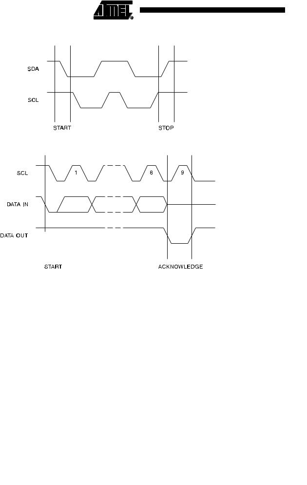
Figure 5. Start and Stop Definition
Figure 6. Output Acknowledge
8 AT24C01A/02/04/08A/16A 
0180Z1–SEEPR–5/07

 AT24C01A/02/04/08A/16A
Device Addressing
Write Operations
The 1K, 2K, 4K, 8K and 16K EEPROM devices all require an 8-bit device address word following a start condition to enable the chip for a read or write operation (refer to Figure 7).
The device address word consists of a mandatory one, zero sequence for the first four most significant bits as shown. This is common to all the EEPROM devices.
The next 3 bits are the A2, A1 and A0 device address bits for the 1K/2K EEPROM. These 3 bits must compare to their corresponding hard-wired input pins.
The 4K EEPROM only uses the A2 and A1 device address bits with the third bit being a memory page address bit. The two device address bits must compare to their corresponding hard-wired input pins. The A0 pin is no connect.
The 8K EEPROM only uses the A2 device address bit with the next 2 bits being for memory page addressing. The A2 bit must compare to its corresponding hard-wired input pin. The A1 and A0 pins are no connect.
The 16K does not use any device address bits but instead the 3 bits are used for memory page addressing. These page addressing bits on the 4K, 8K and 16K devices should be considered the most significant bits of the data word address which follows. The A0, A1 and A2 pins are no connect.
The eighth bit of the device address is the read/write operation select bit. A read operation is initiated if this bit is high and a write operation is initiated if this bit is low.
Upon a compare of the device address, the EEPROM will output a zero. If a compare is not made, the chip will return to a standby state.
BYTE WRITE: A write operation requires an 8-bit data word address following the device address word and acknowledgment. Upon receipt of this address, the EEPROM will again respond with a zero and then clock in the first 8-bit data word. Following receipt of the 8-bit data word, the EEPROM will output a zero and the addressing device, such as a microcontroller, must terminate the write sequence with a stop condition. At this time the EEPROM enters an internally timed write cycle, tWR, to the nonvolatile memory. All inputs are disabled during this write cycle and the EEPROM will not respond until the write is complete (see Figure 8 on page 11).
PAGE WRITE: The 1K/2K EEPROM is capable of an 8-byte page write, and the 4K, 8K and 16K devices are capable of 16-byte page writes.
A page write is initiated the same as a byte write, but the microcontroller does not send a stop condition after the first data word is clocked in. Instead, after the EEPROM acknowledges receipt of the first data word, the microcontroller can transmit up to seven (1K/2K) or fifteen (4K, 8K, 16K) more data words. The EEPROM will respond with a zero after each data word received. The microcontroller must terminate the page write sequence with a stop condition (see Figure 9 on page 11).
The data word address lower three (1K/2K) or four (4K, 8K, 16K) bits are internally incremented following the receipt of each data word. The higher data word address bits are not incremented, retaining the memory page row location. When the word address, internally generated, reaches the page boundary, the following byte is placed at the beginning of the same page. If more than eight (1K/2K) or sixteen (4K, 8K, 16K) data words are transmitted to the EEPROM, the data word address will “roll over” and previous data will be overwritten.
9
0180Z1–SEEPR–5/07
Loading...