

Page 1
ONT-503/506/-512
COMMUNICATIONS TEST & MEASUREMENT SOLUTIONS
Optical Network Tester 40/43 Gb/s Test Solution
Key Features
Optical transport networking
New 40/43 Gb/s networks will allow operators to further enhance transport capacity in the
optical network, extend distances between systems, and improve its flexibility and responsiveness in setting up new high-bandwidth services as well as lowering operating costs for
these services.
40/43 Gb/s optical and electrical interfaces in a single
instrument
SDH STM-256 and SONET OC-768 concatenated and
fully structured signals
OTM0.3 with PRBS or SDH/SONET client
Unframed 39.813 Gb/s and 43.018 Gb/s BER testing
Alarm, error, overhead, and pointer generation and
analysis
Jitter/ Wander generation and analysis for 40/43 Gb/s
March 2009
Market drivers
High-end core routers with 40 Gb/s short reach interfaces are becoming an important
market driver, reducing the number of interconnecting fibers within the central office. Big
benefits are the lower cost, space and power consumption. In long-haul networks, a key
to 40 Gb/s migration is the ability to utilize the existing line system. In metro-regional networks, e.g. city-hoppers applications, 40 Gb/s can also be used very cost effectively.
Challenges
New, high bit rate networks create enormous challenges for equipment vendors not only
because they push the boundaries of physics, but also because every network component
must be perfectly designed, installed and tuned. The point at which networks are installed,
turned up and commissioned will prove critical. A new generation of test equipment
capable of meeting the demands of 40/43 Gb/s systems will be required at each stage of
network design, system verification and validation, network installation, maintenance, and
troubleshooting.
Optical transport test solution
The JDSU ONT-506/512 enables evaluation and characterization of 40/43 Gb/s electrical/
optical devices. The ONT supports unframed BER testing, and framed SDH/SONET/OTN
functional testing including jitter/ wander generation and analysis. The modular concept
starts with 3 slots for 40 Gb/s optical framed and unframed. Further modules can be added
to enable electrical interfaces and jitter/ wander applications. In addition, the programmable hardware architecture allows to add a payload module for the combined OTN with SDH/
SONET client testing and to assure the future-proof for further applications.
WEBSITE: www.jdsu.com/test
Page 2
ONT-5xx 40/43 Gb/s Test Solution
2
Design and conformance testing of NextGeneration transport networks
Multi-application and multi-port configuration
40/43G Solution
SDH/SONET, OTN (optional)•
Unframed testing•
OTN multiplexing option•
40/43G jitter/Wander Solution
SDH/SONET, OTN (optional)•
Highly accurate jitter evaluation according to •
new O.172 Appendices VII + VIII
Wander (optional)•
Page 3

ONT-5xx 40/43 Gb/s Test Solution
3
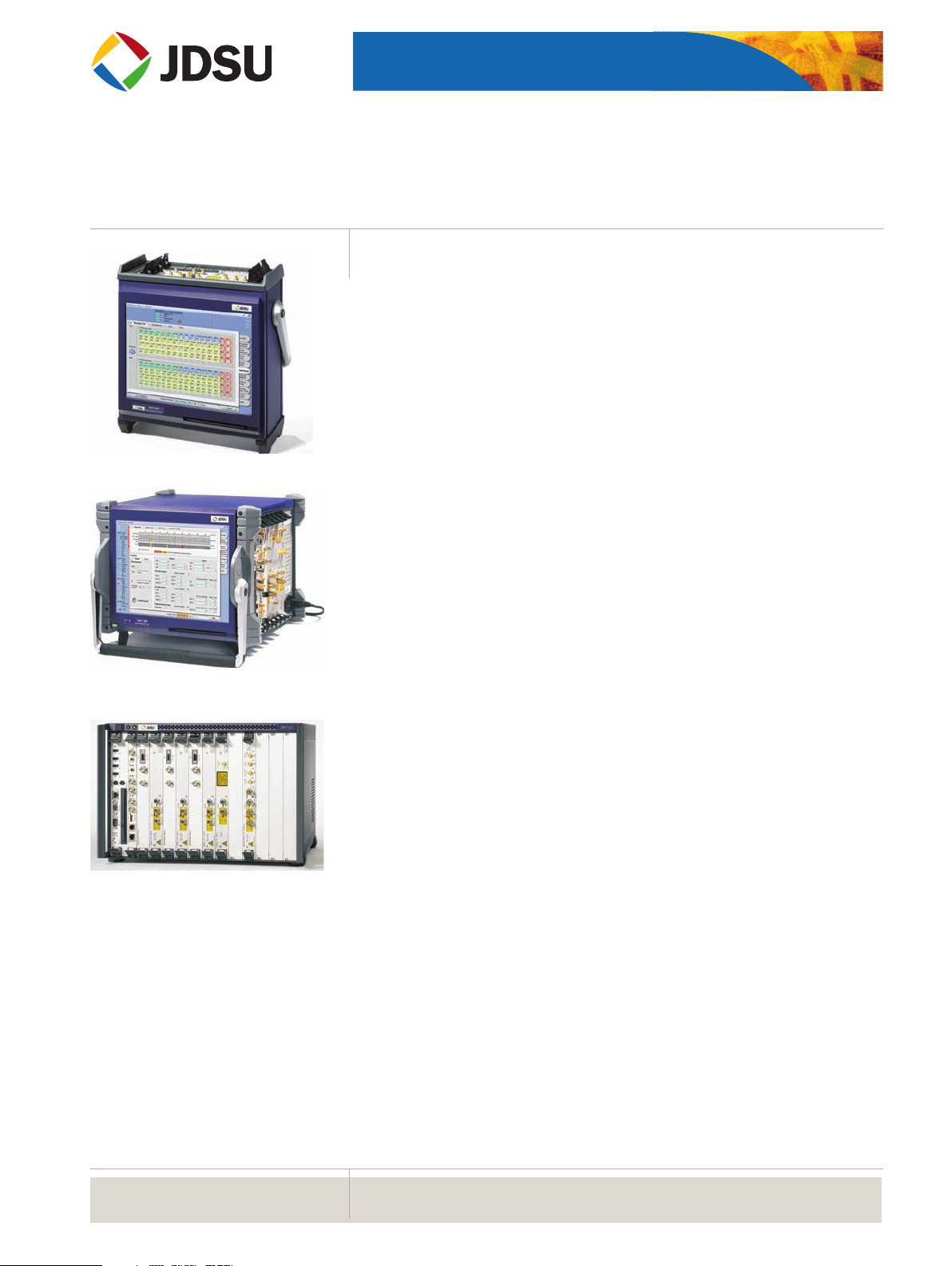
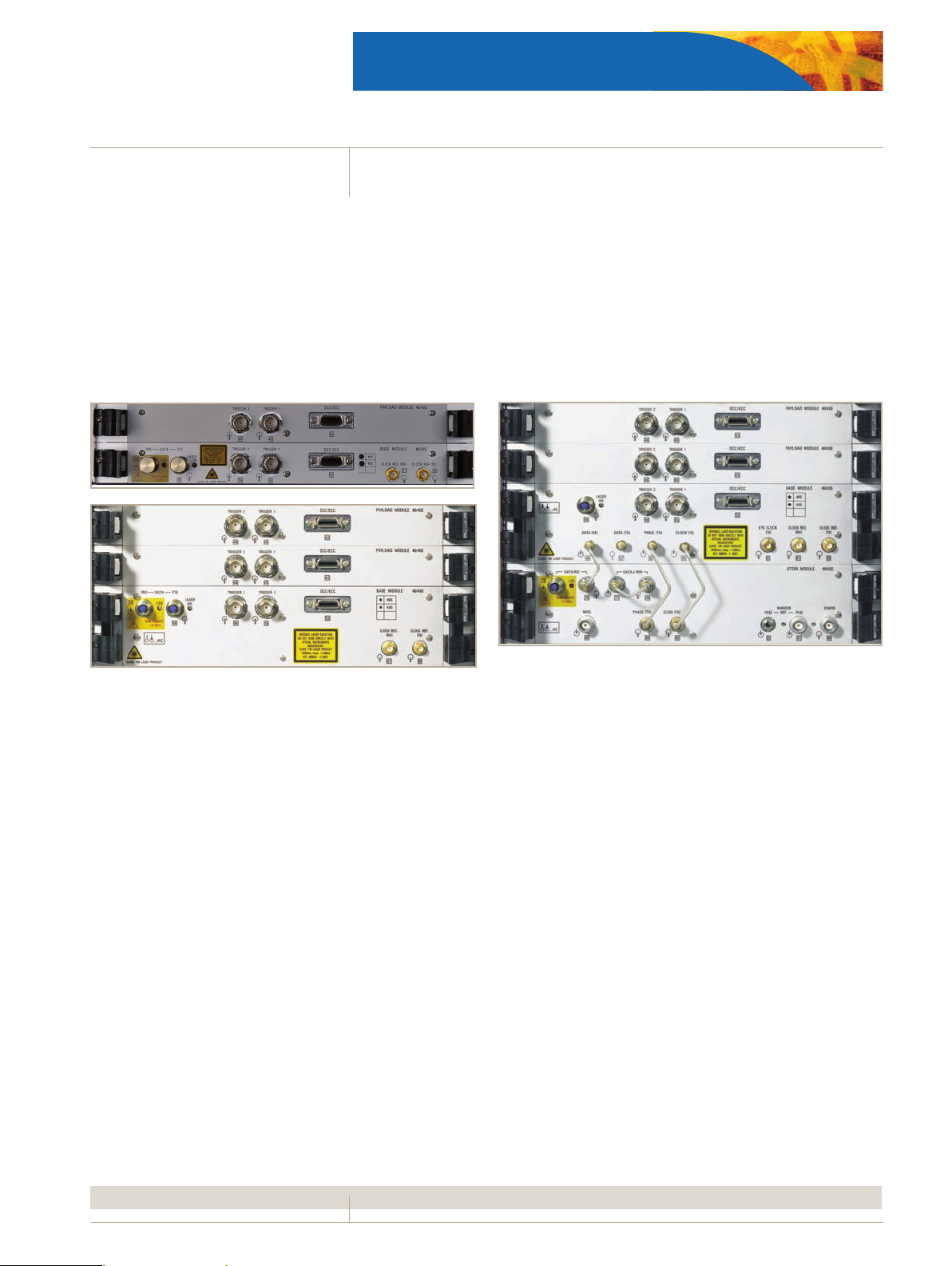
Mainframes
ONT-503 mainframe, 3 slots, 15” TFT display BN 3075/01
ONT-506 mainframe, 6 slots, 15” TFT display BN 3062/01
ONT-512 mainframe, 12 slots, rack mount BN 3061/01
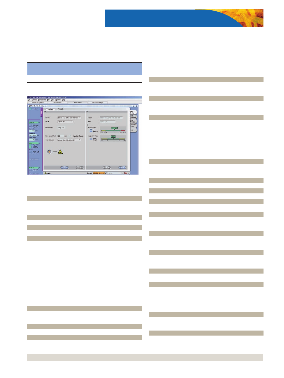
Modules and options Slots required
40/43G solution
40G SDH/SONET Jitter 5 BN 3061/91.61
43G Jitter – BN 3061/91.62
40/43G Wander – BN 3061/93.93
40G SDH/SONET 3 BN 3061/91.51
40G SDH/SONET (ONT-503) 2 BN 3075/91.51
40G SDH/SONET electrical 3 BN 3061/91.54
43G OTN + 1 BN 3061/91.52
43G OTN bulk client – BN 3061/91.53
43G OTN Multiplexing – BN 3061/93.14
43G OTN DPSK with bulk client 3 BN 3061/91.55
43G OTN with SDH/SONET Client + 1 BN 3061/91.56
Page 4

4
ONT-5xx 40/43 Gb/s Test Solution
ONT-5xx Mainframes
Key features
Interchangeable plug-in modules for most flexible use•
Linux operating system•
Easy test automation with full featured driver support•
ONT-503
3 slots to cover multiple ports/applications•
Portable•
Large 15” TFT touchscreen•
ONT-506
6 slots to cover multiple ports/applications•
Desktop•
Large 15” TFT touchscreen•
ONT-512
12 slots to cover multiple ports/applications•
Rack-mount chassis•
‘Plug-in’ modules allow for easy upgrade in the field and exchange
of interfaces among ONT-503 mainframes as well as between ONT506 and ONT-512 mainframes.
All modules use the same software concept. Therefore, developed
scripts can be used and training times for users are minimized.
General specifications
Power supply (nominal range of use)
AC line voltage 100 to 240 V
AC line frequency 50/60 Hz, ± 5%
Power consumption (fully equipped)
ONT-503
ONT-506
ONT-512
Safety class to IEC 61010-1 Class I
Ambient temperature
Nominal range of use +5 to +40 oC/41 to 104 oF
Storage −25 to +45 °C/−13 to +113 °F
Transport −40 to +70 °C/−40 to 158
Weight and dimensions
Dimensions, including handle/bumpers (w × h × d )
ONT-503 360 × 392 × 185 mm, 14.1 × 15.4 × 7.3 in
ONT-506 450 × 335 × 435 mm, 17.7 × 13.2 × 17.1 in
ONT-512 464 × 327 × 523 mm, 18.2 × 12.9 × 20.6 in
7.5 rack unit height is required in a 19’’ rack
Weight, without modules
ONT-503 approx. 10 kg/ 21.5 lb
ONT-506/512 approx. 17 kg/ 37.5 lb
max. 350 VA
max. 650 VA
max. 1000 VA
for stacking
°F
Clock and synchronization
Internal master clock accuracy ± 2.0 ppm
(Exceeds T1.101 stratum 3/3E accuracy)
External synchronization
Connector, unbalanced 75 Ω, BNC jack
Clock source DS1, E1, 1544 kHz, 2048 kHz,
8 kHz, 1 MHz, 5 MHz, 10 MHz
Connector, balanced 110 Ω, Bantam jack
Clock source DS1, E1, 1544 kHz, 2048 kHz
From RX
Each module may use its received signal clock information as reference
for its transmitter.
Clock output
Connector, unbalanced 75 Ω, BNC jack
Connector, balanced 110 Ω, Bantam jack (ONT-506/512)
Instrument operation
The ONT-5xx, which uses the Linux operating system, supports
three types of operation:
Local GUI via built-in touchscreen (ONT-503, ONT-506)•
Local by connecting screen/ mouse/ keyboard (ONT-512)•
Customer script controlled for test automation•
Remote control for test automation via LAN and GPIB•
Remote operation via LAN •
Touchscreen display (ONT-503 and ONT-506)
Large color TFT 15”
Resolution 1024 × 768 (XGA)
Interfaces, storage, data transfer
The ONT-5xx use a Pentium PC as internal controller allowing to run
Linux applications as well.
Interfaces Ethernet (RJ45), 4 x USB,
External keyboard, mouse, VGA, DVI
CD R/W/DVD-ROM drive for data transfer and software update.
PC Pentium M, 1.8 GHz, 1 GB RAM
Hard drive for data/setup storage ≥ 40 GB
Remote control for test automation
The ONT-503 is controlled remotely via SCPI commands sent by the
customer’s program using an Ethernet TCP/IP or a GPIB connection.
The GPIB connection is possible via USB-GPIB cable, provided by
National Instruments.
Modules are addressed independently and in parallel and may be
shared among multiple users. In case of GPIB only one module can
be addressed.
Universal driver libraries facilitate automation with specific support
for individual applications.
Scripting support via Tcl/Tk and C libraries and LabWindows drivers.
The interactive GUI also works in parallel to remote control, so that
it is very easy to develop automated scripts.
Page 5
ONT-5xx 40/43 Gb/s Test Solution
5
40/43G Solutions
Physical layer
40G General
Interface
Line rate 39.813 Gb/s
Line code Scrambled NRZ
Clock generator
Internal accuracy ± 2 ppm
Offset range ± 50 ppm
Offset step size 0.1 ppm
Offset change mode Step, transition ramp
Transition ramp 1 ppm step in 25 ms
Synchronization to external reference signals:
From received signal•
From mainframe see clock and synchronization of the ONT-•
503/506/512 mainframe
40G standard optical
Optical interface
The interface is in accordance with ITU-T G.693, more specificly
VSR2000-3R3 and VSR2000-3R5
Transmitter
Wavelength 1530 to 1565 nm
Output level 0 dBm to +3 dBm
Receiver
Wavelength 1530 to 1565 nm
Sensitivity −6 dBm to +3 dBm
Offset pulling range ± 50 ppm
40G standard electrical
Electrical interface
Impedance AC coupled 50 Ω
Connector type PC 2.92 mm (SMA compatible)
Transmitter
Line code Scrambled NRZ
Output level >200 mVpp
Receiver
Line code Scrambled NRZ
Input level 200 to 600 mVpp
40G Jitter
Optical interface
The interface is in accordance with ITU-T G.693
Transmitter
Wavelength 1530 to 1565 nm
Output level 0 dBm to +3 dBm
Receiver
Wavelength 1530 - 1565 nm
Sensitivity −5 dBm to +3 dBm
Sensitivity for jitter measurement −2 dBm to +2 dBm
Offset pulling range ± 50 ppm
Offset permitted for jitter measurement ± 20 ppm
Eye clock interface
Clock 9.953 GHz
Connector type SMA
Electrical interfaces
Impedance AC coupled 50 Ω
Connector type PC 2.92 mm (SMA compatible)
Generator data signal
Line code Scrambled NRZ
Output level >200 mVpp
Generator clock signal
Output level >200 mVpp
Receiver data signal for digital measurement
Line code Scrambled NRZ
Input level 200 to 600 mVpp
43G General
Interface
Line Rate 43.018 Gb/s
Line code Scrambled NRZ
Clock generator
Internal accuracy ± 2 ppm
Offset range ± 50 ppm
Page 6

6
ONT-5xx 40/43 Gb/s Test Solution
Offset step size 0.1 ppm
Offset change mode Step, transition ramp
Transition ramp 1 ppm step in 25 ms
Synchronization to external reference signals
From received signal•
From mainframe, see clock and synchronization of the •
ONT-503/506/512 mainframe
43G Standard optical
Optical interface
The interface is in accordance with ITU-T G.693, more specificly
VSR2000-3R3F and VSR2000-3R5F
Transmitter
Wavelength 1530 to 1565 nm
Output level 0 dBm to +3 dBm
Reference clock output
Via 50 W SMA connector, with clocking at line rate/64
Receiver
Wavelength 1530 to 1565 nm
Sensitivity −6 dBm to +3 dBm
Offset pulling range ± 50 ppm
Recovered clock output
Via 50 W SMA connector, with clocking at line rate/64
43G Standard electrical
Electrical interfaces
Impedance AC coupled 50 Ω
Connector type PC 2.92 mm (SMA compatible)
Transmitter
Line code Scrambled NRZ
Output level >200 mVpp
Generator reference clock output
Via 50 W SMA connector, with clocking at line rate/64
Receiver
Line code Scrambled NRZ
Input level 200 to 600 mVpp
Recovered clock output
Via 50 W SMA connector, with clocking at line rate/64
43G OTN DPSK (in preparation)
Interface
Line rate 43.016 Gb/s
Line code NRZ-DPSK
Optical interface
Transmitter
Wavelength adjustable λ min. 1528.773 nm
λ max. 1563.863nm
Frequency grid 50 GHz conforming to ITU-T G.694.1
Output level adjustable -1 up to +3 dBm
Step size 0.1 dBm
Reference clock
Via 50 W SMA connector, with clocking at line rate/64
Receiver
Wavelength wide range C-Band compatible
Sensitivity +5 dBm to +10 dBm
Offset pulling range ± 50 ppm
Free spectral range switchable 50 GHz, 66 GHz
Recovered clock output
Via 50 W SMA connector, with clocking at line rate/64
Remark:
40G line rate is not available with this coding.
Service disruption with LOS sensor is only supported with a lower
performance, due to transponder restrictions.
43G Jitter
Optical interface
The interface is in accordance with ITU-T G.693
Transmitter
Wavelength 1530 to 1565 nm
Output level 0 dBm to +3 dBm
Reference clock output
Via 50 W SMA connector, with clocking at line rate/64
Receiver
Wavelength 1530 to 1565 nm
Sensitivity −5 dBm to +3 dBm
Sensitivity for jitter measurement −2 dBm to +2 dBm
Offset pulling range ± 50 ppm
Offset permitted for jitter measurement ± 20 ppm
Recovered clock output
Via 50 W SMA connector, with clocking at line rate/64
Eye clock interface
Clock 10.75 GHz
Connector type SMA
Electrical interfaces
Impedance AC coupled 50 Ω
Connector type PC 2.92 mm (SMA compatible)
Page 7

7
ONT-5xx 40/43 Gb/s Test Solution
Generator data signal
Line code Scrambled NRZ
Output level >200 mVpp
Generator clock signal
Output level >200 mVpp
Receiver data signal for digital measurement
Line code Scrambled NRZ
Input level 200 to 600 mVpp
40/43G Jitter
Standards
Jitter is generated and analyzed in accordance with the following
standards:
ITU-T Recommendation O.172•
Receiver verification and characterization using ITU-T Rec. O.172 •
Appendices VII + VIII with Accuracy Map support
ITU-T Recommendation O.173•
ITU-T Recommendation G.825•
ITU-T Recommendation G.8251•
Jitter analyzer
Measuring ranges/resolution
Peak-Peak I 0 to 2 UIpp/1 mUIpp
Peak-Peak II 1 to 8 UIpp/1 mUIpp
Peak-Peak III 4 to 40 UIpp/10 mUIpp
Peak-Peak IV 20 to 800 UIpp/100 mUIpp
Peak-Peak V 400 to 14000 UIpp/1 UIpp
RMS I 0 to 1 UI/0.1 mUI
RMS II 0.5 to 4 UI/0.1 mUI
RMS III 2 to 20 UI/1 mUI
RMS IV 10 to 400 UI/10 mUI
RMS V 200 to 7000 UI/100 mUI
Measurement accuracy (fixed error in 2 UI range)
20/80 kHz to 320 MHz 150 mUIpp
16 MHz to 320 MHz 50 mUIpp
Built-in filters
High-pass filters 20 kHz, 80 kHz, 16 MHz
Low-pass filter 320 MHz
Demodulator output
Connector type BNC, 50 Ω
Jitter application
Supports all manual and automatic measurements for jitter evaluations.
Jitter measuring modes
Current values (continuous measurement): Peak-Peak, positive
peak, negative peak, RMS
Maximum values (gated measurement): Peak-Peak, positive peak,
negative peak
Logged values (repetitive measurements): Peak-Peak, positive peak,
negative peak
Jitter generator
Built-in modulation generator
Jitter modulation signal Sine wave, 10 Hz to 320 MHz
Jitter amplitude up to 12800 UIpp
Step width 0.001 UI
Generation accuracy (16 MHz to 320 MHz)
External modulation input
Connector type BNC, 50 Ω
Modulation frequency 0.1 Hz to 320 MHz
Input voltage range 0 to 632 mVpp (0 dBm)
40 mUIpp
Phase hits
The instrument detects when the programmable threshold for
positive and negative jitter values is exceeded and the result indicates how often the threshold was exceeded.
Jitter versus time
This function is used to record variations of jitter with time and
allows the positive and negative peak values, peak-to-peak values,
and RMS values to be displayed versus time. Duration is up to 99
days.
Automatic jitter measurements
Maximum tolerable jitter (MTJ)
The jitter module automatically determines the maximum jitter
amplitude tolerated by the DUT at selected jitter frequencies. The
maximum permissible jitter amplitude can be precisely determined
using a successive method. The module determines the exact limit
value. Several error sources are selectable. Standard tolerance
masks are available and can be edited.
Page 8
8
ONT-5xx 40/43 Gb/s Test Solution
Fast maximum tolerable jitter (Fast-MTJ)
This extremely fast measurement tests the device under test for
conformance to the standard tolerance mask limits for maximum
tolerable jitter. The editable frequency/amplitude values are set
sequentially and the test pattern is monitored for the permitted
threshold by the receiver. The result of each measurement is shown
in a table as a status message.
Selective jitter transfer function (JTF)
The JTF shows the ratio of the jitter amplitude at the output of the
device under test (DUT) and at the input at various frequencies.
Standard tolerance masks are available and can be edited.
40/43G Wander
Fully complies with or exceeds the requirements of ITU-T O.172.
This software option is only available in conjunction with 40G SDH/
SONET jitter and the 43G jitter option which enables wander generation and analysis at the different bit rates.
Unbalanced BNC 75 Ω
Clock signal 1.544, 2.048, 5, 10 MHz
Data signal 1.544, 2.048 Mb/s
Wander measuring modes
Time interval error (TIE) numerical and graphical, peak-peak wander numerical.
TIE values are recorded and available for MTIE/TDEV evaluations
and frequency offset and drift rate measurements with graphs and
built-in masks that comply with Telcordia GR-253, GR-1244, ANSI
T1.101, ETSI ETS 300 462, EN 302 084, ITU-T O.172, and G.810 to
G.813 recommendations.
Automatic wander measurements
Maximum tolerable wander (MT W)
This application tests the DUT for conformance to the standard
tolerance mask limits for wander tolerance and is available in connection with the wander generator.
The device under test is subjected to wander at several amplitudes
and frequencies and the output signal is monitored for different
error sources. The measurement point is then marked as “Pass” (no
alarms or errors detected) or “Fail” (alarms or errors detected).
Interface and Unframed Testing
Wander generator
Modulation signal Sine wave
Amplitude range 0.1 to 1024000 UI
Amplitude step width 0.1 UI
Frequency range 10 µHz to 10 Hz
Frequency step width 1 µHz
Wander analyzer
Four different sampling rates are available for detailed analysis versus time:
Sampling rate – Low-pass filter
1/s – 0.1 Hz, 30/s – 10 Hz (O.172), 60/s – 20 Hz, 1000/s – 100 Hz
(O.172)
Wander reference signal input
Balanced Bantam 110 Ω
Clock signal 1.544, 2.048 MHz
Data signal 1.544, 2.048 Mb/s
Unframed testing
With the possibility to generate and analyze unframed test signals
the application space for testing with ONT family can be extended
to earlier testing phases in the optical component area but also for
verification of real transparent signals.
Transmitter
Generator reference clock output
Via 50 W SMA connector, with clocking at line rate/64
Page 9

9
ONT-5xx 40/43 Gb/s Test Solution
Receiver
Recovered clock output
Via 50 W SMA connector, with clocking at line rate/64
Displays the current optical input level and the min/max values
with timestamp.
Displays the current signal frequency and offset and the min/max
values with timestamp.
Generator
31
Test pattern PRBS: 2
2
31
-1 inv., 223-1 inv., 215-1 inv., 211-1 inv., 27-1 inv.
-1, 223-1, 215-1, 211-1, 27-1,
(Conforming to ITU-T O.150)
Error insertion
Type Bit errors
Trigger Single, rates from 1 x 10
-3
to 1 x 10
-12
With mantissa equal 1
Alarm insertion
Type LOS
Trigger Continuous
Trigger output
Type Off, Laser on
Pulse output Event present, logical high
Level TTL compatible, high >2.4 V, low <0.8 V
Connector BNC, 75 Ω
Analyzer
Analysis of test pattern PRBS: 2
2
31
-1 inv., 223-1 inv., 215-1 inv., 211-1 inv., 27 -1 inv.
31
-1, 223-1, 215-1, 211-1, 27-1,
(Conforming to ITU-T O.150)
Error measurement
Type Bit errors
Alarm detection
Type LOS, Pattern Loss
Resolution 100 ms
Result display of errors and alarms
Numerical display
Count, ratio and duration are displayed for each error
Duration is displayed for each alarm
Tabular display
Display of all results with time stamps
Criteria Start, stop, duration, count
Intermediate bit error
In addition to the long term bit error measurement, intermediate results are available.
Interval 1 s up to 3600 s,
Results Current/previous interval,
Count and ratio
Trigger output
Type Off, LOS alarm
Pulse output Event present, logical high
Level TTL compatible, high >2.4 V, low <0.8 V
Connector BNC, 75 Ω
40G SDH/SONET
SDH/SONET application
SDH/SONET testing
Generation/evaluation of STM-256 signal according to ITU-T G.707
Generation/evaluation of OC-768 signal according to ANSI T1.105
Mapping
SDH VC-4-256c, VC-4-64c, VC-4-16c, VC-4-4c, VC-4, AU-3/VC-3
SONET STS-768c SPE, STS-192c SPE, STS-48c SPE,
STS-12c SPE, STS-3c SPE, STS-1 SPE
Generator
Generator modes
Free definable foreground•
All channels identical •
Background selectable mapping, depending on foreground chan-•
nel with definable path overhead and Null pattern as payload
Auto signal structure
Receiver analyses the signal structure (mapping, payload, traces)
automatically for easy configuration of the test channel.
Test pattern PRBS: 2
2
31
-1 inv., 223-1 inv., 215-1 inv., 211-1 inv.
(Conforming to ITU-T O.150)
Programmable word Length 32 bits
31
-1, 223-1, 215-1, 211-1,
Page 10

ONT-5xx 40/43 Gb/s Test Solution
10
Error insertion
Types
SDH Random, FAS, B1, B2, B3, MS-REI, HP-REI, bit errors
SONET Random, FAS, B1, B2, B3, REI-L, REI-P, bit errors
Trigger Single, rates
Error Min rate Max rate Stepping Mapping
Random 1 × 10
FAS 1 × 10
B1 1 × 10
B2 1 × 10
MS-REI,
REI-L
B3 1 × 10
B3 1 × 10
HP-REI,
REI-P
HP-REI,
REI-P
Bit error 1 × 10
Burst error once and continuous M errored frames followed by
N error-free frames. All errors except random and bit errors
N, M = 1 to 8000000 or 125 µs to 1000 s
Alarm generation
Type:
SDH LOF, RS-TIM, MS-AIS, MS-RDI, AU-AIS, AU-LOP, HP-UNEQ,
HP-TIM, HP-PLM, HP-RDI, HP-RDI-C, HP-RDI-S, HP-RDI-P
SONET LOF, AIS-L, RDI-L, TIM-L, AIS-P, LOP-P, UNEQ-P,
TIM-P, PLM-P, RDI-P, RDI-P-C, RDI-P-S,
RDI-P-P, PDI-P
Trigger LOS, TIMs on/off
All others on/off or burst
Burst once and continuous
M frames with alarm ON, N frames with alarm OFF
N, M = 1 to 800000 or 125 µs to 1000 s
Trigger output
Generates an external trigger signal at generation of the internal
event.
Types
SDH Off, frame trigger, MS-AIS, AU-AIS, B1, B2, B3, Bit errors
SONET Off, frame t rigger, AIS-L, AIS-P, B1, B2, B3, Bit errors
Pulse output Event present, logical high
Level TTL compatible, high >2.4 V, low <0.8 V
Connector BNC, 75 Ω
1 × 10
1 × 10
1 × 10
-10
1 × 10⁻³Exponential –
-12
-12
-12
-12
-12
-12
-12
-12
-12
-3
1 × 10
1.61 × 10
1.61 × 10
1.61 × 10
-6
-3
1 × 10
-3
1 × 10
-6
-3
1 × 10
-6
-3
1 × 10
1 × 10⁻³Exponential –
0.1 –
0.1 –
0.1 –
0.1 –
0.1 STM-VC-4-256c,
STS-1-768cSPE
0.1 STM-VC-3,
STS-1-SPE
0.1 STM-VC-4-256c,
STS-1-768cSPE
0.1 STM-AU-3/VC-3,
STS-1-SPE
Overhead generator
The stimulus of different overhead byte pattern is an important
part of verification and interoperability testing. Network elements
(NE) should respond in the defined manner and any responses then
conveyed by a different overhead byte.
Statically programmable bytes
A1-A2 unscrambled•
RSOH/SOH all bytes except B1•
MSOH/LOH all bytes except B2, H1...H3•
POH all bytes except B3•
Display of overhead on the GUI.
Trace identifier
J0, J1 programmable 1 byte, 16 bytes with CRC or 64 byte sequence
Generation of pointer actions
Generation of pointer actions at the AU/STS level
New pointer value setting with or without NDF•
Offset simulation in ppms•
Single, periodical and alternating pointer increment/decrement •
Pointer sequences with different types•
SS-bits definable•
Analyzer
Test pattern PRBS: 231-1, 223-1, 215-1, 211-1,
2
(conforming to ITU-T O.150)
Programmable word Length 32 bits
“Live traffic” mode ignores pattern loss and bit error that allows analysis of live traffic without trouble indication
Error measurements
SDH FAS, B1, B2, B3, MS-REI, HP-REI, Bit errors
SONET FAS, B1, B2, B3, REI-L, REI-P, Bit errors
31
-1 inv., 223-1 inv. , 215-1 inv., 211-1 inv.
Page 11

11
ONT-5xx 40/43 Gb/s Test Solution
Alarm detections
SDH OOF, LOF, MS-AIS, MS-RDI, RS-TIM, AU-AIS, AU-LOP,
HP-TIM, HP-UNEQ, HP-PLM, HP-RDI, Pattern Loss
SONET OOF, LOF, AIS-L, RDI-L, TIM-L, AIS-P, LOP-P,
TIM-P, UNEQ-P, PLM-P, RDI-P, PDI-P, PLM-P,
ERDI-P-Payload, ERDI-P-Server,
ERDI-P-Connect, Pattern Loss
Resolution 100 ms
Result display of errors and alarms
Numerical display
Count, ratio and duration are displayed for each error
Duration is displayed for each alarm
Tabular display
Display of all results with time stamps
Criteria Start, stop, duration, count
Graphical display
Display of all events as bar graphs versus time. Cursors allow easy
identification and zooming (in and out) on results. Filters enable
event selection.
Time axis Second, minute, hour
Intermediate bit error
In addition to the long term bit error measurement, intermediate results are available.
Interval 1 s up to 3600 s,
Results Current/previous interval,
Count and ratio
Trigger output
Generates an external trigger signal at the detection of the received
event.
Types
SDH Off, frame trigger, LOF alarm, OOF alarm, MS-AIS alarm,
AU-AIS alarm, B1, B2, B3, Bit errors
SONET Off, frame trigger, LOF alarm, SEF alarm, AIS-L alarm,
AIS-P alarm, B1, B2, B3, Bit errors
Pulse output Event present, logical high
Level TTL compatible, high >2.4 V, low <0.8 V
Connector BNC, 75 Ω
Overhead analyzer
Display of Overhead on the GUI.
Service disruption test
To analyze service disruption times, the ONT-5xx generates a highspeed event list as a result of all detected events.
Sensor to trigger service disruption test, selectable
Errors
SDH FAS, B1, B2, MS-REI, B3, HP-REI, bit errors/pattern loss
SONET FAS, B1, B2, REI-L, B3, REI-P, bit errors/patt. loss
Alarms
SDH LOS, LOF, OOF, MS-AIS, MS-RDI, AU-AIS, AU-LOP ,
HP-UNEQ, HP-PLM, HP-RDI,
SONET LOS, LOF, SEF, AIS-L, RDI-L, AIS-P, LOP-P, UNEQ-P,
PLM-P, PDI-P, RDI-P
Event sample resolution 100 µs
Separation time 0.1 ms to 100000 ms
Separation time starts at the end of the last event. Separation time
is used to determine if the following event is a continuation of the
same disruption (event occurs within separation time) or the start
of the next disruption (event occurs after separation time has
elapsed).
Result display of disruptions
Numerical display
Total Number of disruptions, begin timestamp of first
Disruption, end timestamp of last disruption,
Shortest disruption time (with timestamp)
Longest disruption time (with timestamp)
Average disruption time
The threshold to identify a violation of allowed service
Disruption time can be set in the range of 0 ms to 100000 ms
Tabular display
Service disruption events with start/stop times and duration.
Three logging modes available (no logging; disruption events
only; disruption and causing sensor events)
Transfer delay analysis
Message evaluation (TIM/PLM)
J0, J1 1 byte, 16 bytes with CRC or 64 byte sequence•
J0, J1 clear text display•
TIM evaluation: exception value editable as criterion for TIM•
C2 signal label clear text selection•
PLM Evaluation: exception value editable as criterion for PLM•
Page 12

12
ONT-5xx 40/43 Gb/s Test Solution
Transfer delay measurements by special payload pattern in the
Range of 0 to 40 s.
Transfer delay can be measured even between different ports
within the same mainframe.
Numerical display
Current transfer delay with accuracy of 1 µs and
Resolution 100 ns
Minimum transfer delay (with timestamp)
Maximum transfer delay (with timestamp)
Pointer analysis
AU/STS Pointer
Numerical display
Value, count of increments, decrements, NDF.
Tabular display
Display of all events with time stamps
Criteria Start, stop, duration, count
Performance monitoring
For SDH
Performance monitoring G.826
EB, BBE, ES, EFS, SES, and UAS are evaluated. Pass/fail assessments
based on line length allocation of 0.1 to 100%.
The SES and UAS thresholds are user-programmable. In-service
measurement (ISM) of the near end and the far end of a selected
path, as well as out-of-service (OOS) measurements, are supported.
Performance monitoring G.828 and G.829
The G.828 defines error performance parameters for international
synchronous paths.
EB, BBE, ES, EFS, SES, and UAS are evaluated. Pass/fail assessments
are based on a line length allocation of 0.1 to 100%.The SES and UAS
thresholds are user-programmable. The SEP can be switched off
for assessment. G.829 defines error performance events and block
structures for SDH multiplex and regenerator sections.
Storage depth of one byte or K1/K2 combination
Post trigger up to 256 value changes
Pre trigger up to 256 value changes
Trigger conditions Pre, post, center
Trigger events User defined byte value,
(compare, not compare, don’t care)
bit mask
43G OTN
OTN application
OTN testing
The OTN application runs on the Interface module and the payload
board and allows generation and analysis of an OTM0.3 signal.
Detailed parameters can be manipulated and evaluated in different OTN levels. Its payload supports both framed SDH/SONET and
unframed clients.
The test set provides signal analysis and manipulation (alarm, error,
overhead), Forward Error Correction (FEC) generation and analysis
as well as FEC error testing. In addition to this, the full analysis capabilities of SDH and SONET are available for OTN client analysis.
For SONET
Evaluation of ES, EFS, SES, UAS and SEFS (GR 253, T1.231) ESA, ESB
Byte capture SOH/TOH
To analyze the SOH/TOH functions, it is necessary to capture individual bytes vs. time, allowing detection of errors or short term
changes with frame level resolution. The capture function is started
by a selectable trigger.
Values for one/two selected bytes are stored and can be accessed
subsequently in a table of values.
Particularly in capturing the APS sequences, bytes K1 and K2 are
displayed in clear text.
Selectable bytes for SOH/TOH All bytes
Captured parameters Byte value, number of frames and
Correspondent time
Generator
OPU3 mapping of client signals:
CBR40G with SDH/SONET client (optional, BN 3061/91.52 or •
BN 3061/91.56)
– STM-256/STS-768 signal internally generated.
– Generation see “40G SDH/SONET application” page 9.
PRBS test signal •
– PRBS 2
27-1 inv. (conforming to ITU-T O.150)
– Digital word 32 bit free programmable
Null client•
OTN multiplexing (optional, see page 16)•
All clients can be mapped bit-synchronous or asynchronous. •
31
-1, 223-1, 215-1, 27-1, 231-1 inv., 223-1 inv., 215-1 inv.,
Page 13

13
ONT-5xx 40/43 Gb/s Test Solution
Client offset – stuffing
The asynchronous SONET and SDH client offset can be adjusted
within the ± 65 ppm range and the stuffing rate of the client can
thus be manipulated.
Overhead
Overhead bytes (frame alignment/OTU/ODU/OPU)
All bytes statically programmable except MFAS, SM BIP, PM BIP, •
TCM1...6 BIP
Additional possibilities for SM TTI, PM TTI, TCM1...6 TTI (Trail Trace •
Identifier):
Sequence consisting of the SAPI (16 bytes) and
DAPI (16 bytes) and the operator specified (32 bytes).
User designed payload structure identifier (PSI), payload type •
identifier clear text and support of MSI
One OH byte can be selected for a freely defined sequence of •
16/32/64/128/256 bytes
FTFL free definable forward/backward (FW/BW) fault indication •
and operator identifier
Error insertion
Type Random, FAS, MFAS
SM BIP-8, SM BEI, PM BIP-8, PM BEI
TCMi BIP-8, TCMi BEI (i = 1 to 6)
Bit errors (only available with PRBS test signal)
Trigger Single , rate, burst , burst continuous
Burst error M frames errors, N frames error free,
M and N = 0 to 2
Rate
Error name Min rate Max rate Stepping
Random 1 × 10
Bit 1 × 10
FAS 4.9 × 10
MFAS 3.0 × 10
SM BIP 1 × 10
SM BEI 1 × 10
PM BIP 1 × 10
PM BEI 1 × 10
TCMi BIP 1 × 10
TCMi BEI 1 × 10
-10
-12
-12
-11
-12
-12
-12
-12
-12
-12
1 × 10
1 × 10
1 × 10
1 × 10
6.6 × 10
6.6 × 10
6.6 × 10
6.6 × 10
6.6 × 10
6.6 × 10
-3
-3
-3
-3
-5
-5
-5
-5
-5
-5
Exponential
Exponential
0.1
0.1
0.1
0.1
0.1
0.1
0.1
0.1
BIP masks
The position and number of bit errors in the bytes can be selected.
Valid for SM BIP, PM BIP, TCMi BIP (i = 1 to 6)
BEI value
To stress the BEI evaluation of the DUT receiver the BEIs can be set
to values 0 to 15
Valid for SM BEI, PM BEI, TCMi BEI (i = 1 to 6)
Alarm generation
Type LOF, OOF, LOM, OOM
OTU-AIS, ODU-AIS, ODU-OCI, ODU-LCK, SM BDI,
SM IAE, SM BIAE, PM-BDI, PM-TM
FW-SD, FW-SF, BW-SD, BW-SF
TCMi-LTC, TCMi-BDI, TCMi-BIAE, TCMi-TIM (i = 1 to 6)
Trigger
Continuously All alarms
Burst once/
Burst continuous all errors except LOF, OOF, OOM, SD, SF, TIMs
Burst alarms M frames with alarm, N frames no alarm,
M = 1 to 2
N = 0 to 2
OTU FEC
The FEC generation can be switched on and off. Using the OTU FEC
field, FEC according to the Reed-Solomon (255,239) algorithm is
performed on the generated frame. With data blocks consisting of
239 data bytes and 16 FEC field bytes, up to 16 byte errors can be
detected or 8 byte errors be corrected.
FEC error inser tion modes
FECcorrectable, FECuncorrectable•
FECstress: This extremely helpful function allows maximum stress •
tests within a short time frame.
The maximum possible number of errors that the device under
test (DUT) should still be able to correct is inserted into the OTU
31
frame.
FECadvanced
FECadvanced allows the user to define a detailed position for error
insertion in the OTU frame. Correction capability testing below and
above the correction limit can be performed.
Selectable parameters: row, subrow, errored bytes per subrow,
Start position in subrow, byte error mask
Analyzer
OPU-3 mapping of client signals:
CBR40G with SDH/SONET client (optional, BN 3061/91.52) •
– STM-256/STS-768 signal.
– Analysis see 4”0G SDH/SONET applications” page 9.
PRBS test signal •
– PRBS 2
2
31
-1, 223-1, 215-1, 27-1, 231-1 inv., 223-1 inv. 215-1 inv.,
7
-1 inv., (conforming to ITU-T O.150)
– Digital word 32 bit free programmable
Null client•
OTN multiplexing (optional, see page 16)•
All clients can be de-mapped bit-synchronous and asynchronous
Stuffing of the client
Display of client offset in ppm
31
31
Page 14

14
ONT-5xx 40/43 Gb/s Test Solution
Stuffing counts
Positive, negative, sum count, duration of affected seconds
Overhead
Overhead evaluation (frame alignment/OTU/ODU/OPU)
Display of the complete overhead•
SM TTI, PM TTI, TCM1…6 TTI display of the 64 byte ASCII sequence •
of SAPI, DAPI and Operator field
One sequence of up to 256 bytes can be captured and displayed •
for a selectable OH byte
Display payload structure identifier (PSI) bytes, payload type iden-•
tifier (PT) clear text and support of MSI
Editable PT expectation value as mismatch criterion•
FTFL forward/backward (FW/BW) fault indication and operator •
identifier fields
Trace references
Set of SAPI and DAPI expectation values in traces SM TTI, PM TTI, •
TCM1…6 TTI
Select evaluation type of the received signal: SAPI or DAPI or SAPI/•
DAPI
General Communication Channel Capture (GCC, in preparation)
The management information between network element and
termination equipment is transported in the GCCs in the OTN
overhead. With this feature, the transmitted information can be
captured in real-time.
Captured fields GCC0, GCC1, GCC2, GCC1+2
Captured format Raw
Capture size up to 500 MB
Trigger Manual
Error measurement
Validation of data for error measurement occurs after frame alignment, descrambling, and FEC computation and correction (if
enabled).
Alarm detection
Types LOF, OOF, LOM, OOM
OTU-AIS, ODU-AIS, ODU-OCI, ODU-LCK, SM BDI, SM IAE, SM
BIAE, SM TIM, PM-BDI, PM TIM
FW-SD, FW-SF, BW-SD, BW-SF
TCMi-LTC, TCMi-BDI, TCMi-IAE, TCMi-BIAE, TCMi-TIM (i = 1 to 6)
CL-LOSS (Client signal loss of synchronization)
PT-MISM
Error detection
Types FAS, MFAS, SM BIP, SM BEI, PM BIP, PM BEI
TCMi BIP, TCMi BEI (i = 1 to 6)
Bit error (only available for PRBS/digital word testing signal)
Resolution 100 ms
Result display of errors and alarms
Numerical display
Count, ratio and duration are displayed for each error
Duration is displayed for each alarm
Tabular display
Display of all results with time stamps
Criteria Start, stop, duration, count
Graphical display
Display of all events as bar graphs versus time. Cursors allow easy
identification and zooming (in and out) on results. Filters enable
event selection.
Time axis Second, minute, hour
Intermediate bit error
In addition to the long term bit error measurement, intermediate results are available.
Interval 1 s up to 3600 s,
Results Current/previous interval,
Count and ratio
OTU FEC
The FEC analysis and correction can be switched on and off. Using
the OTU FEC field, FEC according to the Reed-Solomon (255,239)
algorithm is performed on the received frame. With data blocks
consisting of 239 data bytes and 16 FEC field bytes, up to 16 byte
errors can be detected or 8 byte errors be corrected.
Error detection
Type FECcorrectable bit, FECcorrectable code word,
FECuncorrectable code word
Result display of errors
Numerical display
Count, ratio and duration are displayed for each error
Tabular display
Display of all results with time stamps
Criteria Start, stop, duration, count
Page 15

15
ONT-5xx 40/43 Gb/s Test Solution
Graphical display
Display of all events as bar graphs versus time. Cursors allow easy
identification and zooming (in and out) on results. Filters enable
event selection.
Time axis Second, minute, hour
Service disruption test
To analyze service disruption times, the ONT-5xx generates a highspeed event list as a result of all detected events.
Sensor to trigger service disruption test, selectable:
Errors
Types MFAS, SM-BEI, PM-BIP, PM-BEI, payload errors
Event sample resolution 100 µs
Alarms
Types LOS, LOM, OOM, SM-IAE, SM-BDI, SM-BIAE, ODU-AIS,
ODU-OCI, ODU-LCK, PM-BDI
Separation time 0.1 ms to 100000 ms
Separation time starts at the end of the last event. Separation time
is used to determine if the following event is a continuation of the
same disruption (event occurs within separation time) or the start
of the next disruption (event occurs after separation time has
elapsed).
Tabular display:
Service disruption events with start/stop times and duration.
Three logging modes available (no logging; disruption events only;
disruption and causing sensor events)
Transfer delay analysis
Transfer delay measurements by special payload pattern in the
range of 0 to 40 s.
Transfer delay can be measured even between different ports
within the same mainframe.
Numerical display
Current transfer delay with accuracy of 1 µs and resolution 100 ns
Minimum transfer delay (with timestamp)
Maximum transfer delay (with timestamp)
Result display of disruptions
Numerical display
Total Number of disruptions, begin timestamp of first disruption,
end timestamp of last disruption,
Shortest disruption time (with timestamp)
Longest disruption time (with timestamp)
Average disruption time
The threshold to identify a violation of allowed service disruption
time can be set in the range of 0 ms to 100000 ms
Page 16
16
ONT-5xx 40/43 Gb/s Test Solution
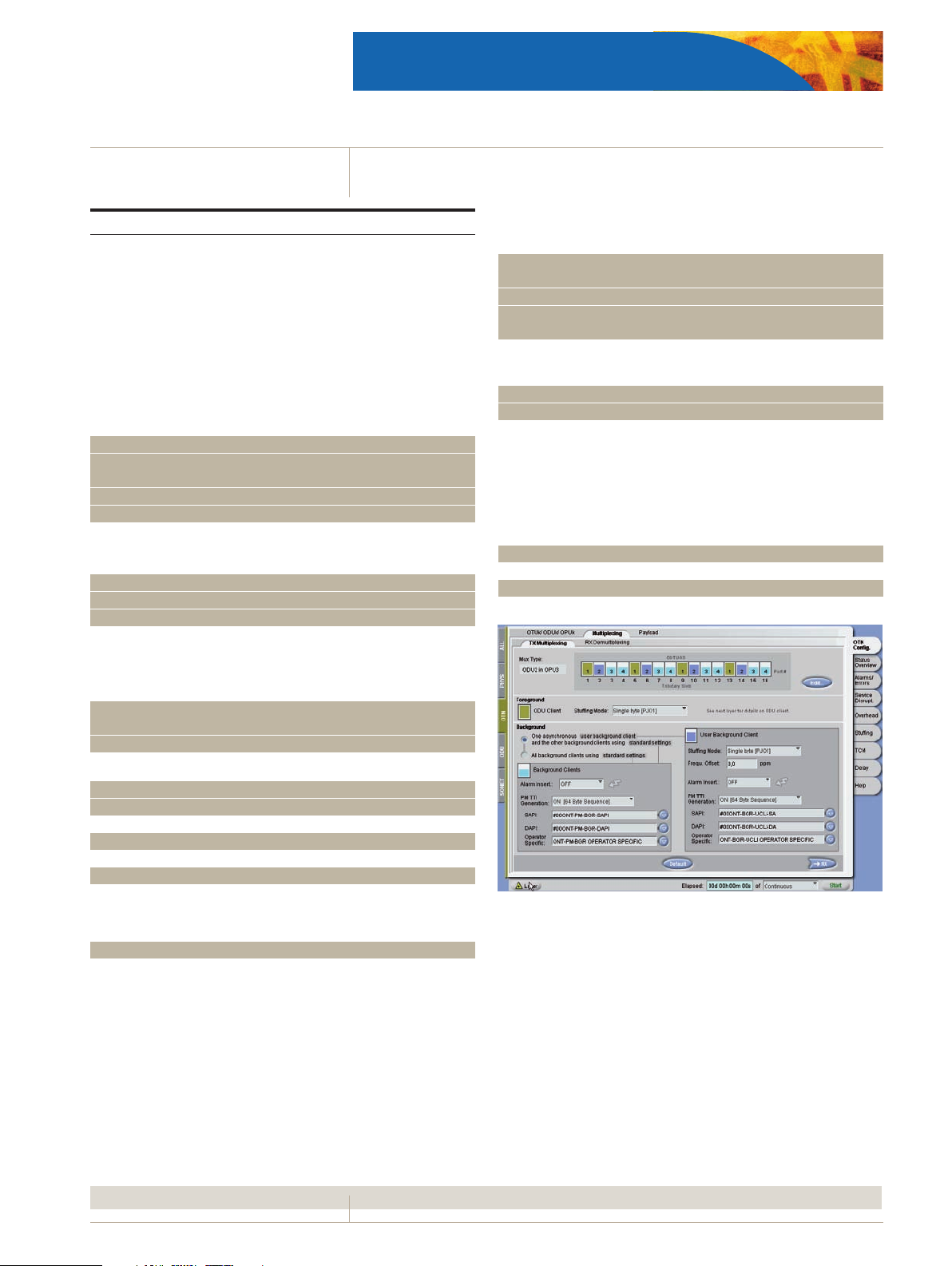
OTN Multiplexing
As OTN moving forward from a point to point technology to a
network technology additional features getting implemented.
In special OTN-Multiplexing is to mention as such a feature. The
ONT-503/-506/-512 will support ODU2/1 multiplexing in ODU3.
Software option 43G OTN Mulitplexing BN 3061/93.14
OTU3
Generator
Signal structure
Foreground Full structured ODU1/ODU2
With one of the following clients Bulk client,
SDH/SONET (optional)
Bulk client PRBS: 2
2
31
-1 inv., 223-1 inv., 215-1 inv., 211-1 inv., 27-1 inv.
User Background Structured ODU1/ODU2
With user defined PM-TTI and a NULL client payload
Generation enable/disable
Background The remaining time slots are filled ODU1/ODU2
With a user defined PM-TTI, identical all channels
and a NULL client payload
User background and background
can be overwritten by ODU-OCI, ODU-AIS, and ODU-LCK
Only one multiplex type is supported at a time ODU1 or ODU2. TX
and RX not coupled.
Time slot allocation Foreground and user background can be
Free allocated, background channels
Are automatically allocated.
Client offset stuffing
Following modes a supported Negative, positive,
Double positive
Foreground Default 0 ppm to client bit rate
Offset range ± 65 ppm
User Background Enabled, default 0 ppm to client bit rate
Offset range ± 65 ppm
Background No stuffing support
Other generator capabilities are identical to OTU3 for the Foreground with following restrictions:
No SM support, because only on OTU available.
No FEC support, because only on OTU available.
31
-1, 223-1, 215-1, 211-1, 27,
Analyzer
Signal structure
Foreground Full structured ODU1/ODU2
With one of the following clients Bulk client,
SDH/SONET client (optional)
Bulk client PRBS: 2
2
31
-1 inv., 223-1 inv., 215-1 inv., 211-1 inv., 27-1 inv.
31
-1, 223-1, 215-1, 211-1, 27,
Time slot allocation Foreground can be free allocated
Client offset stuffing
Following modes a supported Negative, positive,
Double positive
Displays of client offset in ppm
Stuffing counts
Positive, double positive, negative, sum count, duration of affected
seconds
Other analyzer capabilities are identical to OTU3 for the foreground
with following restrictions:
No SM support, because only at OTU layer available
No FEC support, because only at OTU layer available
No GCC capture
See “OTN application” page 12
Page 17

17
Ordering information
ONT-5xx 40/43 Gb/s Test Solution
Module 40/43G solution
SDH/SONET Application
For ONT-506/512
BN 3061/91.51 40G SDH/SONET
STM-256, OC-768, unframed 40G
3 slots
BN 3061/91.54 40G SDH/SONET electrical
STM-256, OC-768, unframed 40G
3 slots
For ONT-503
BN 3075/91.51 40G SDH/SONET
STM-256, OC-768, unframed 40G
2 slots
OTN Application
BN 3061/91.52 43G OTN
OTM.03, unframed 43G,
SDH/SONET and bulk-client
1 slot in addition
Requires one of the following:
40G SDH/SONET BN 3061/91.51 or BN 3075/91.51 or
43G Jitter BN 3061/91.62
BN 3061/91.53 43G OTN bulk with bulk client
OTM.03 unframed 43G,
Bulk-client
Software option
Requires one of the following:
40G SDH/SONET BN 3061/91.51 or BN 3075/91.51 or
43G Jitter BN 3061/91.62
BN 3061/91.55 43G OTN DPSK
OTM.03, framed 43G
Bulk client
3 slots
BN 3061/91.56 43G OTN with SDH/SONET client
Adds to 43G OTN a full SDH/SONET client
Requires BN 3061/91.55 or BN 3061/91.53
1 slot
BN 3061/93.14 43G OTN Multiplexing
ODU2 and ODU1 in ODU3
with SDH/SONET or bulk client
Requires BN 3061/91.52 or /91.56
OTN Application with DPSK
BN 3061/91.55 43G OTN DPSK with bulk client
OTM.03 with NRZ-DPSK
Unframed 43G
OTU3 with bulk client
3 slots
BN 3061/91.56 43G OTN with SDH/SONET client
Adds to OTU3 the capability to have a SDH/SONET
client
1 slot
Jitter/Wander Application
BN 3061/91.61 40G SDH/SONET Jitter
STM-256, OC-768, unframed 40G
5 slots
BN 3061/91.62 43G Jitter
Unframed jitter at 43G
No additional slot required
Requires the following:
40G SDH/SONET Jitter BN 3061/91.61
OTN framed signals require:
43G OTN BN 3061/91.52
BN 3061/93.93 Wander 40/43G
Software option
Requires the following:
40G SDH/SONET Jitter BN 3061/91.61 and
optional 43G Jitter BN 3061/91.62
Page 18

ONT-5xx 40/43 Gb/s Test Solution
18
Ordering information
Optical Connectors
For built-in optics, the following adapter types are available. One
adapter per interface is included in the initial order and is user selectable.
Measuring adapter
BN 2060/00.51 FC, FC-PC, FC-APC
BN 2060/00.58 SC, SC-PC, SC-APC
BN 2060/00.32 ST type (AT&T)
BN 2060/00.51 DIN 47256
BN 2060/00.53 E 2000 (Diamond)
BN 2060/00.59 LC, F-3000 (PC-APC)
Optical attenuators
BN 2239/90.30 FC-PC, 10 dB, 1310/1550 nm
BN 2239/90.38 SC, 10 dB, 1310/1550 nm
JDSU offers a wide range of optical power meters, sources and attenuators. Contact your local sales representative for details.
Page 19

19
Ordering information
NOTES:
ONT-5xx 40/43 Gb/s Test Solution
Page 20

ONT-5xx 40/43 Gb/s Test Solution
ONT
ONT
DUT
DUT
DUT
22
VOA
1N
1N
TBF
22
VOA
OPM
OPMOA
22
Fiber
spool
Scope
MAP
Related products
TestPoint Family
TestPoint offers a flexible and cost effective telecom and datacom test solution for Production and Service Verification Testing (SVT). It consists of a modular platform that provides
versatility in configuring interface types, transmission rates, protocols, and port density.
One of the TestPoint’s key attributes is support for multiple rates on single modules.
It is available in three chassis formats: a lightweight, fixed interface TS-10, a 3-slot TS-30,
and a 17-slot TS-170. TestPoint provides 1G/2G/4G/10G Fibre Channel support and Ethernet features from 10 Mb/s up to 10 Gigabit Ethernet.
Transport protocol coverage includes SDH/SONET up to 40G, and Optical Transport Network (G.709) including overclocked rates.
Multiple Application Platform (MAP)
With over 20 unique modules, MAP enables users to manipulate and control optical
transmission signals (independent of rate or format) and enables testing of transmission
quality as a function of parameters such as Average Power, OSNR and Polarization state.
Optical switches and optical splitter modules may be added to enable automation interfaces for multiple devices and/or multiple signal sources.
The modular platform is available in 3 or 8 slot chassis with GPIB or RS-232 interfaces.
ActiveX and LabView drivers are also provided. Rack mount kits and a reverse mount
system enable clean factory test integration and rear fiber exit when needed.
2×2: optical switch (cross)
OA: optical amplifier
OPM: optical power meter
VOA: variable optical attenuator
1×N: 1:N switch
TBF: tunable bandpass filter
OLA-55M Optical Level Controller
The OLA-55M contains both attenuator and power level function making test set-up simple and eliminating the need to connect several instruments, cables and couplers.
See OLA-55M data sheet for details.
Handheld Fiber Inspection Microscope
Many light transmission problems occur as a result of improper fiber connectors. The
Fiber Microscope reflects details of scratches and any contamination of connector end
surfaces. The light weight microscope is equipped with universal push-pull adapter.
Test & Measurement Regional Sales
Product specifications and descriptions in this document subject to change without notice. © 2009 JDS Uniphase Corporation 10143237 005 0309 ONT5xx-40G.DS.OPT.TM.AE March 2009
NORTH AMERICA
TEL: +1 866 228 3762
FAX: +1 301 353 9216
LATIN AMERICA
TEL: +1 954 688-5660
FAX: +1 954 3454668
ASIA PACIFIC
TEL: +852 2892 0990
FAX: +852 2892 0770
EMEA
TEL: +49 7121 86 2222
FAX: +49 7121 86 1222
www.jdsu.com/test
 Loading...