

Page 1
Technical Datasheet
RF/Microwave Signal
Generators
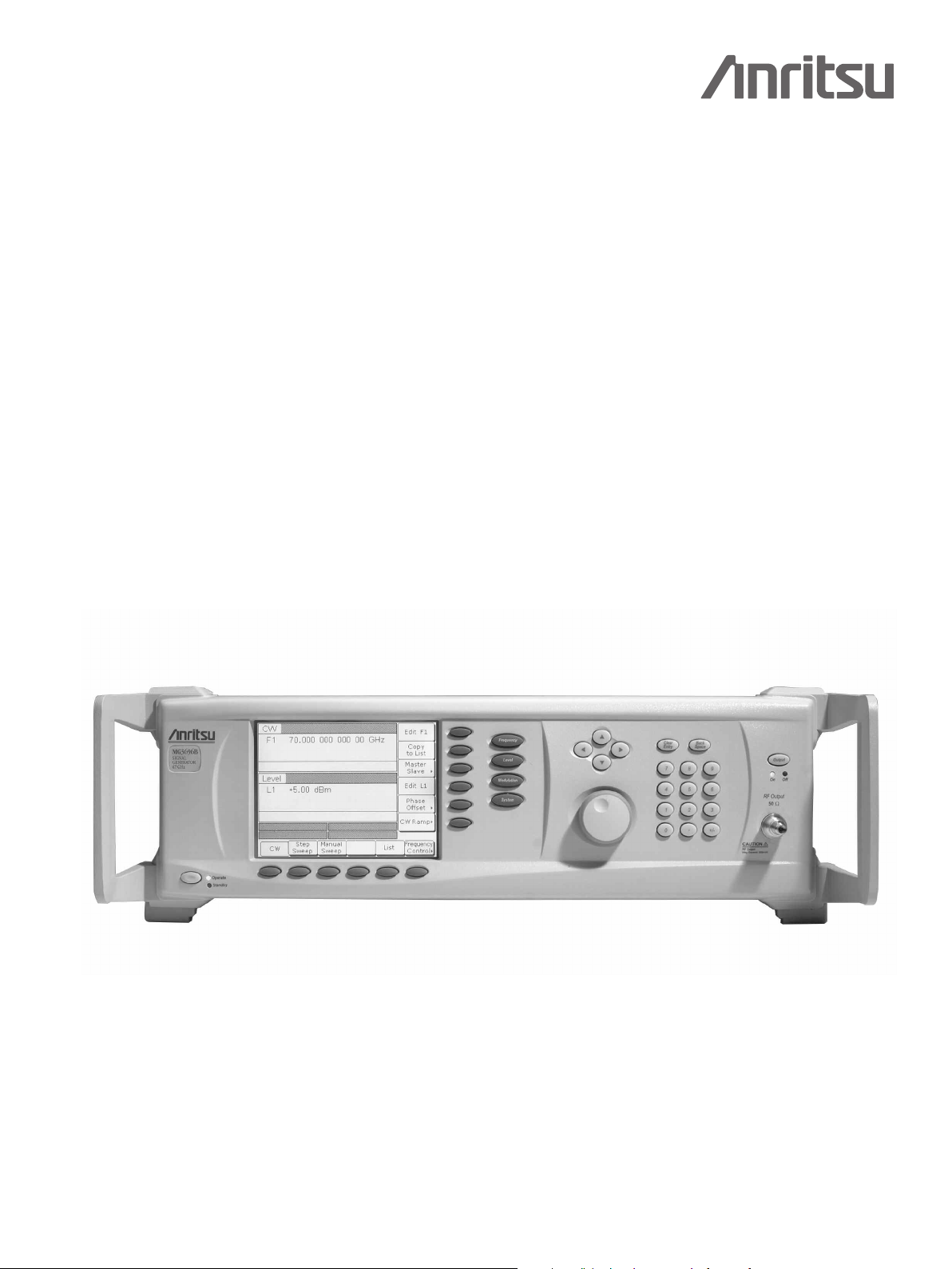
MG3690B
RF/Microwave Signal Generator, 0.1 Hz to 70 GHz/325 GHz
Introduction
The MG3690B is the “ideal microwave signal generator” because it offers unsurpassed frequency coverage, leveled output
power, spectral purity, switching speed, modulation performance, size, upgradeability, reliability, and service. Our signal
generators are configurable for a broad range of applications from R&D to manufacturing and depot repair. Anritsu provides
you a total solution including proven reliability and standard 3 year warranty plus pre- and post-sale support that is the best
in the industry.
The Ideal Signal Generator
Page 2
Specifications
The specifications in the following pages describe the warranted performance of the
g
enerator for 25 ± 10°C. Typical specifications describe expected, but not warranted,
performance based on sample testing.
Frequency Coverage
Model/Option No. Frequency Coverage Output Type
G3691B 2 to 10 GHz K(f)
M
G3692B 2 to 20 GHz K(f)
M
MG3693B 2 to 30 GHz K(f)
G3694B 2 to 40 GHz K(f)
M
G3695B 2 to 50 GHz V(f)
M
MG3696B 2 to 67 GHz* V(f)
ption 4 10 MHz to 2.2 GHz Model No. Dependent
O
ption 5 10 MHz to 2 GHz Model No. Dependent
O
Option 22 0.1 Hz to 10 MHz Model No. Dependent
Operational to 70 GHz
*
Options 4 and 5: Frequency extension down to 10 MHz
Two options are available to extend the 2 GHz low end frequency limit of the base
models down to 10 MHz. Option 4 uses a digital down-converter (DDC) with successive
divide-by-two circuitry. It offers the best phase noise performance of the two choices, at
the expense of some analog performance <500 MHz. In that range, analog sweep mode
is not available, and pulse modulation performance is specified as typical. In addition,
frequency and phase modulation mod index is scaled by the division ratio of each band
of the DDC. Option 5 maintains all analog performance by using a heterodyne mixing
down-converter
.
Option 22: Frequency extension down to DC
If frequency coverage down to 0.1 Hz is desired, Option 22 can be added with either
Option 4 or 5. Option 22 uses Direct Digital Synthesis (DDS) for CW and Step Sweep
modes of operation. Modulation and analog sweep are not available in the DDS band.
Frequency resolution <10 MHz is 0.02 Hz. Output power across the complete instrument
frequency range is degraded by 2 dB.
CW Mode
Output: Twenty independent, presettable CW frequencies
(F0 – F9 and M0 –M9).
Accuracy: Same as internal or external 10 MHz time base.
Internal Time Base Stability:
With Aging: <2 x 10⁻⁹/day (<5 x10
With Temperature: <2 x 10
–10
x 10
(<2
/deg C with Option 16)
–10
/day with Option 16)
–
8
/deg C over 0˚C to 55˚C
Resolution: 0.01 Hz
External 10 MHz Reference Input: Accepts external 10 MHz ±50 Hz (typical), 0 to
+20 dBm time base signal. Automatically disconnects the internal high-stability time-base
option, if installed. BNC, rear panel, 50
Ω impedance. Selectable Bandwidth for best
phase noise immunity or best phase tracking performance.
10 MHz Reference Output: 1 Vp-p into 50Ω, AC coupled.
Rear panel BNC; 50
Ω impedance.
Phase Offset: Adjustable in 0.1 degree steps.
Electronic Frequency Control (EFC) Input: –5V to +5V input range;
–7
.Fout Hz/V sensitivity (typical); ≤250 Hz Modulation BW; Rear panel BNC;
5 x 10
Impedance
High
Phase-Locked Step Sweep Mode
idth:
Sweep W
sweep range is phase-locked.
Accuracy: Same as internal or external 10 MHz time base.
Resolution (Minimum Step Size): 0.01 Hz
Independently selected, 0.01 Hz to full range. Every frequency step in
Linear/Log Sweep: User-selectable linear or log sweep.
I
n log sweep, step size logarithmically increases with frequency.
Steps: User-selectable number of steps or the step size.
Number of Steps: Variable from 1 to 10,000
Step Size: 0.01 Hz to the full frequency range of the instrument.
(If the step size does not divide into the selected frequency range,
the last step is truncated.)
Dwell Time Per Step: Variable from 1 ms to 99 seconds
Fixed Rate Sweep: Allows the user to set the total time of the sweep,
including lock time. Variable from 20 ms to 99 seconds.
Analog Sweep Mode (Option 6)
Sweep Width: Independently selected from 1 MHz to full frequency range. With Option
4, Digital Down Converter, Analog sweep is only available ≥500 MHz. Analog sweep is
not available <10 MHz with Option 22.
Accuracy: The lesser of ±30 MHz or (±2 MHz + 0.25% of sweep width)
for Sweep Speeds of
≤50 MHz/ms (typical)
Sweep Time Range: 30 ms to 99 seconds
Alternate Sweep Mode
Sweeps alternately in step sweep between any two sweep ranges. Each sweep range
may be associated with a power level.
Manual Sweep Mode
Provides stepped, phase-locked adjustment of frequency between sweep limits. Userselectable number of steps or step size.
List Sweep Mode
Under GPIB control or via the front panel, up to 4 tables with 2000 non-sequential
frequency/power sets can be stored and then addressed as a phase-locked step sweep.
One table of 2000 points is stored in non-volatile memory, all other tables are stored in
volatile memory
.
Programmable Frequency Agility
Under GPIB control, up to 3202 non-sequential frequency/power sets can be stored and
then addressed as a phase-locked step sweep. Data stored in volatile memory.
Markers
Up to 20 independent, settable markers (F0 – F9 and M0 – M9).
Video Markers: +5V or –5V marker output, selectable from system menus. AUX I/O
connector, rear panel.
Intensity Markers: Produces an intensity dot on analog display traces, obtained by a
momentary dwell in RF sweep, in analog sweeps of <1s.
Marker
Accuracy:
Same as sweep frequency accuracy
.
Marker Resolution:
Analog Sweep:
1MHz or Sweep Width/4096 which ever is greater.
Step Sweep: 0.01 Hz.
Sweep Triggering
Sweep triggering is provided for Analog Frequency Sweep, Step Frequency Sweep,
Frequency Sweep, and
List
Auto: Triggers sweep automatically.
External: Triggers a sweep on the low to high transition of an external TTL signal. AUX
I/O connector
, rear panel.
Single: Triggers, aborts, and resets a single sweep. Reset sweep may be selected to be
at the top or bottom of the sweep.
CW Power Sweep.
2
Page 3

eneral
G
Stored Setups: Stores front panel settings and nine additional front-panel setups in a
n
on-volatile RAM. A system menu allows saving and recalling of instrument setups.
Whenever the instrument is turned on, control settings come on at the same functions
and values existing when the instrument was turned off.
Memory Sequencing Input: Accepts a TTL low-level signal to sequence through ten
s
tored setups. AUX I/O connector, rear panel.
Self-Test: Instrument self-test is performed when Self-Test soft-key is selected. If an
error is detected, an error message is displayed in a window on the LCD identifying the
probable cause and remedy.
Secure Mode: Disables all frequency and power level state displays. Stored setups
saved in secure mode remain secured when recalled. Mode selectable from a system
menu and via GPIB.
P
arameter Entry:Instrument-controlled parameters can be entered in three ways:
keypad, rotary data knob, or the
keypad is used to enter new parameter values; the rotary data knob and the cursorcontrol key are used to edit existing parameter values. The
cursor-control key move the cursor left and right one digit under the open parameter.
The rotary data knob or the ∧ and ∨ touch pads will increment or decrement the digit
position over the cursor. Controlled parameters are frequency, power level, sweep time,
dwell time, and number of steps. Keypad entries are terminated by pressing the
appropriate soft key. Edits are terminated by exiting the edit menu.
Reset: Returns all instrument parameters to predefined default states or values.
Any pending GPIB I/O is aborted. Selectable from the system menu.
Master/Slave Operation: Allows two output signals to be swept with a user-selected
frequency offset. One instrument controls the other via AUX I/O and SERIAL I/O
connections. Requires a Master/Slave Interface Cable Set (Part No. ND36329).
User Level Flatness Correction: Allows user to calibrate out path loss due to external
switching and cables via entered power table from a GPIB power meter or calculated
data. When user level correction is activated, entered power levels are delivered at the
point where calibration was performed. Supported power meters are
ML2438A, and ML4803A and HP 437B, 438A, and 70100A. Five user tables are
available with up to 801 points/table.
Warm Up Time:
From Standby: 30 minutes.
From Cold Start (0 deg C): 120 hours to achieve specified frequency stability with aging.
∧ and ∨ touch pads of the cursor-control key. The
∧ and ∨ touch pads of the
Anritsu ML2437A,
Instruments disconnected from AC line power for more than 72 hours require
30 days to return to specified frequency stability with aging.
Power: 85-264 Vac, 48-440 Hz, 250 VA maximum
Standby: With ac line power connected, unit is placed in standby when front panel
power switch is released from the OPERATE position.
Weight: 18 kg maximum
Dimensions: 133 H x 429 W x 450 D mm
Warranty: 3 years from ship date
emote Operation
R
All instrument functions, settings, and operating modes (except for power on/standby)
a
re controllable using commands sent from an external computer via the GPIB
(IEEE-488 interface bus).
GPIB Address: Selectable from a system menu
I
EEE-488 Interface Function Subset:
Source Handshake:
Acceptor Handshake: AH1
Talker: T6
Listener: L4
S
ervice Request:SR1
Remote/Local: RL1
Parallel Poll: PP1
Device Clear: DC1
Device Trigger: DT1
C
ontroller Capability:C0, C1, C2, C3, C28
Tri-State Driver: E2
GPIB Status Annunciators: When the instrument is operating in Remote, the GPIB
status annunciators (listed below) will appear in a window on the front panel LCD.
Remote: Operating on the GPIB (all instrument front panel keys except for the SYSTEM
key and the RETURN TO LOCAL soft-key will be ignored).
L
LO (Local Lockout):Disables the RETURN TO LOCAL soft-key. Instrument can
be placed in local mode only via GPIB or by cycling line power.
Emulations: The instrument responds to the published GPIB commands and responses
Anritsu Models 6600, 6700,and 6XX00-series signal sources. When emulating
of the
another signal source, the instrument will be limited to the capabilities, mnemonics, and
parameter resolutions of the emulated instrument.
SH1
Environmental (MIL-PRF-28800F, class 3)
Storage Temperature Range: –40 to +75°C
Operating Temperature Range: 0 to +50°C
Relative Humidity: 5% to 95% at 40°C
Altitude: 4,600 meters, 43.9 cm Hg
EMI: Meets the emission and immunity requirements of
EN61326: 1998
EN55011: 1991/CISPR-11:1990 Group 1 Class A
EN61000-4-2: 1995 – 4 kV CD, 8 kV AD
EN61000-4-3: 1997 – 3 V/m
EN61000-4-4: 1995 – 0.5 kV SL, 1 kV PL
EN61000-4-5: 1995 – 1 kV – 2 kV L-E
EN61000-4-6: 1996
EN61000-4-11: 1994
ibration:
V
Safety Directive: EN 61010-1: 1993 + A1: 92 + A2: 95
Random, 5-500 Hz, 0.015-0.0039g2/Hz PSD
Sinusoidal, 5-55 Hz, 0.33 mm displacement
3
Page 4

Frequency Switching Time
Spectral Purity
efinitions
D
F
ree Running Mode:
(Step or List Sweep)
tsw= Switching Time, Unlocked
= Locked Time = 1ms + t
t
lk
dw
tdw= Dwell Time, after locking. Selectable, 1 ms minimum
tlk(min) = 2 ms
S
ingle Frequency Trigger Mode:
(List, non-sequential, and CFx modes)
All specifications apply at the lesser of +10 dBm output or maximum specified leveled
o
utput power, unless otherwise noted.
purious Signals
S
Harmonic and Harmonically-related:
Frequency Range Standard
.1 Hz to 10 MHz (Option 22) <–30 dBc
0
0 MHz to
1
100 MHz to ≤2.2 GHz (Option 4)
>
10 MHz to
50 MHz to
>
>2 GHz (2.2 GHz w/Option 4) to ≤20 GHz
>20 GHz to
40 GHz to ≤50 GHz (MG3695B)
>
>40 GHz to ≤67 GHz (MG3696B)
–30 dBc typical with high power Option 15
*
=
20 GHz to 21 GHz and 39 - 40 GHz – 20 dBc typical
00 MHz (Option 4)
≤1
≤50 MHz (Option 5)
GHz (Option 5)
≤2
≤40 GHz
–40 dBc
<
<–50 dBc
–30 dBc
<
<–40 dBc
<–60 dBc*
–40 dBc*
<
<–40 dBc*
<–25 dBc
=
Non-harmonics:
Frequency Range Standard
0.1 Hz to 10 MHz (Option 22) <–30 dBc
0 MHz to
1
10 MHz to ≤2 GHz (Option 5)
2 GHz (2.2 GHz w/Option 4) to ≤67 GHz
>
.2 GHz (Option 4)
≤2
–60 dBc
<
<–40 dBc
<–60 dBc
Switching Time (tsw)
t
(ms)
*
sw
5 ms + 1 ms/GHz step not starting at, or crossing dwell frequencies
7 ms + 1 ms/GHz (typical) step not starting at, or crossing band switching frequencies
8 ms + 1 ms/GHz (typical) step starting at, or crossing band switching frequencies
Band Switching Dwell Frequencies: 2 (2.2 w/Opt. 4), 10, 20, 40 GHz
Filter Switching Dwell Frequencies: 3.3, 5.5, 8.4, 13.25, 25, 32 GHz
<2.2 GHz w/Opt. 4: 12.5, 15.625, 22.5, 31.25, 43.75, 62.5,
125, 175, 250, 350, 500, 700,
MHz
*Not applicable with FM mode active
Condition
1050,
1500
87.5,
Power Line and Fan Rotation Spurious Emissions (dBc):
Frequency <300 Hz
10 to ≤500 MHz (Option 4)
>500 to ≤1050 MHz (Option 4)
≤2200 MHz (Option 4)
>1050 to
0.01 to ≤8.4 GHz
>8.4 to ≤20 GHz
≤40 GHz
>20 to
>40 to ≤67 GHz
<–68 <–72 <–72
<–62 <–72 <–72
<–56 <–66 <–66
<–50 <–60 <–60
<–46 <–56 <–60
<–40 <–50 <–54
<–34 <–44 <–48
Offset from Carrier
300 Hz to 1 kHz >1 kHz
Residual FM (CW and Step Sweep modes, 50 Hz - 15 kHz BW):
ual FM (Hz RMS)
Frequency Range
≤8.4 GHz
>8.4 to 20 GHz <40 <220
>20 to ≤40 GHz
>40 to ≤67 GHz
Resid
Option 3 Standard
<40 <120
<80 <440
<160 <880
Residual FM (Analog Sweep and Unlocked FM modes, 50 Hz - 15 kHz BW):
Resid ual FM (kHz RMS)
Frequency Range
0.01 to ≤20 GHz
>20 GHz to ≤40 GHz
>40 GHz to
≤67 GHz
Unlocked Narrow
FM mode
<5 <25
<10 <50
<20 <100
Unlocked Wide
FM mode or
Analog Sweep (typ.)
AM Noise Floor:
Typically <–145 dBm/Hz at 0 dBm output and offsets >5 MHz from carrier.
4
Page 5

ingle-Sideband Phase Noise*
S
Single-Sideband Phase Noise (dBc/Hz): (Typical)
requency Range
F
≥0.1 Hz to <10 MHz (Option 22)
0 MHz to <500 MHz (Option 4)
≥1
≥500 MHz to <2.2 GHz (Option 4)
0 MHz to <2 GHz (Option 5)
≥1
GHz to ≤6GHz
≥2
6 GHz to
>
10 GHz to
>
>20 GHz to
40 GHz to
>
0 GHz
≤1
0 GHz
≤2
≤40 GHz
7 GHz
≤6
00 Hz
1
90 (–110) –120 (–125) –130 (–139) –130 (–141)
–
94 (–98) –106 (–115) –104 (–114) –120 (–127)
–
82 (–90) –94 (–102) –92 (–100) –108 (–117)
–
–77 (–85) –88 (–92) –85 (–91) –100 (–108)
77 (–79) –88 (–92) –86 (–90) –102 (–112)
–
–73 (–78) –86 (–91) –83 (–90) –102 (–107)
66 (–72) –78 (–84) –77 (–83) –100 (–104)
–
–60 (–66) –75 (–78) –72 (–77) –94 (–98)
–54 (–60) –69 (–72) –64 (–71) –88 (–92)
Single-Sideband Phase Noise (dBc/Hz) – Option 30: (Typical)
requency Range
F
≥0.1 Hz to <10 MHz (Option 22)
0 MHz to <500 MHz (Option 4)
≥1
≥500 MHz to <2.2 GHz (Option 4)
0 MHz to <2 GHz (Option 5)
≥1
≥2 GHz to ≤6 GHz
>6 GHz to
≤10 GHz
>10 GHz to
>20 GHz to
>40 GHz to
≤20 GHz
≤40 GHz
≤67 GHz
10 Hz 100 Hz 1 kHz 10 kHz 100 kHz 1 MHz
60 (–100)
–
–77 (–82)
–64 (–70)
64 (–68)
–
–54 (–61)
–52 (–60)
–45 (–49)
–45 (–49)
–37 (–41)
Offset from Carrier
kHz
1
Offset from Carrier
90 (–1
–
0) –
1
–99 (–100) –1
–86 (–92) –98 (–106) –98 (–107) –110 (–119) –135 (–143)
83 (–86) –93 (–100) –93 (–100) –100 (–108)
–
–77 (–82) –93 (–98) –93 (–99) –102 (–112) –130 (–136)
–73 (–78) –93 (–96) –93 (–99) –105 (–112) –128 (–136)
–68 (–73) –86 (–91) –86 (–93) –100 (–108) –125 (–135)
–63 (–67) –80 (–85) –80 (–87) –94 (–102) –119 (–129)
–57 (–61) –74 (–79) –74 (–81) –88 (–96) –113 (–123)
120 (–125) –130 (–139) –130 (–141)
0 (–118)
1
–1
0 (–117)
1
0 kHz
1
00 kHz
1
130 (–141)
–
–122 (–129) –142 (–146)
111 (–115)
–
Single-Sideband Phase Noise (dBc/Hz) – Option 3: (Typical)
Frequency Range
≥0.1 Hz to <10 MHz (Option 22)
≥10 MHz to ≤15.625 MHz (Option 4)
>15.625 MHz to
>31.25 MHz to
>62.5 MHz to ≤125 MHz (Option 4)
>125 MHz to
>250 MHz to
>500 MHz to ≤1050 MHz (Option 4)
>1050 MHz to ≤2200 MHz (Option 4)
≥10 MHz to <2 GHz (Option 5)
≥2 GHz to ≤6 GHz
>6 GHz to ≤10 GHz
>10 GHz to ≤20 GHz
>20 GHz to
>40 GHz to ≤67 GHz
*Phase noise is specified and guaranteed only with internal reference. In External Reference mode, the phase noise of the external supplied reference, and the selected external reference bandwidth,
will dictate the instrument phase noise performance. Phase noise is not degraded when adding high power Option 15.
≤31.25 MHz (Option 4)
≤62.5 MHz (Option 4)
≤250 MHz (Option 4)
≤500 MHz (Option 4)
≤40 GHz
10 Hz 100 Hz 1 kHz 10 kHz 100 kHz 1 MHz
–60 (–100) –90 (–110) –120 (–125) –130 (–139) –130 (–141) –130 (–141)
–105 (–118) –126 (–133) –139 (–145) –142 (–148) –141 (–148) –145 (–149)
–99 (–114)
–90 (–111) –114 (–121) –129 (–143) –136 (–146) –136 (–146) –144 (–152)
–88 (–98) –108 (–116) –127 (–130) –135 (–143) –133 (–143) –144 (–148)
–84 (–90) –102 (–110) –125 (–129) –132 (–137) –130 (–135) –143 (–147)
–77 (–83) –99 (–103) –123 (–128) –125 (–131) –124 (–129) –142 (–146)
–71 (–77) –93 (–100) –118 (–122) –121 (–126) –119 (–124) –138 (–144)
–66 (–71) –86 (–96) –112 (–116) –115 (–121) –113 (–119) –135 (–143)
–64 (–78) –83 (–88) –100 (–106) –102 (–1
–54 (–60) –77 (–86) –104 (–108) –108 (–113) –107 (–112) –130 (–136)
–52 (–57) –73 (–81) –100 (–105) –107 (–114) –107 (–113) –128 (–136)
–45 (–49) –68 (–76) –94 (–100) –102 (–108) –102 (–107) –125 (–135)
–45 (–49) –63 (–70) –92 (–94) –98 (–102) –98 (–101) –119 (–129)
–37 (–40) –57 (–69) –86 (–88) –92 (–96) –90 (–95) –113 (–123)
–120 (–127) –134 (–144) –137 (–147) –137 (–147) –145 (–150)
Offset from Carrier
10)
–102 (–108) –1
1
1 (–1
15)
5
Page 6
RF Output
MG3690B
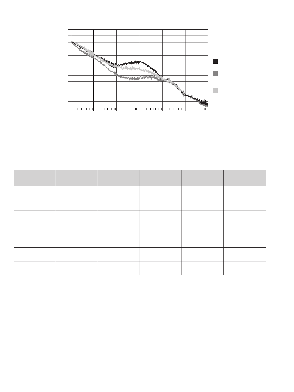
SSB Phase Noise
L(f ) dBc/Hz
10 GHz
100 Hz 1 kHz 10 kHz 100 kHz 1 MHz
10 MHz
–40
–50
–60
–70
–
80
–
90
–100
–110
–120
–130
–140
–150
Standard
Performance
Ultra-Low
Performance
(with Option 3)
Option 30
Power level specifications apply at 25 ±10˚C.
Maximum Leveled Output Power***:
Model Number Configuration
MG3691B
MG3692B
MG3693B
MG3694B
MG3695B
MG3696B
* ≤2.2 GHz with Option 4
** >2.2 GHz with Option 4
*** For output power with Option 22, 0.1 Hz to 10 MHz coverage, derate all specifications by 2 dB
**** Typical 60 to 67 GHz
w/opt 4 or 5
STD
w/opt 4 or 5
STD
STD
w/opt 4 or 5
STD
STD
STD
w/opt 4 or 5
STD
STD
STD
w/opt 4 or 5
STD
STD
w/opt 4 or 5
STD
STD
Typical MG3690B single sideband phase noise at 10 GHz carrier.
Standard and Ultra-Low performance with Option 3.
Frequency Range
(GHz)
<2* GHz
≥2** to ≤10 GHz
<2* GHz
≥2** to ≤10 GHz
>10 to ≤20 GHz
<2* GHz
≥2** to ≤10 GHz
≤20 GHz
>10 to
>20 to
≤30 GHz
<2* GHz
≥2** to ≤10 GHz
≤20 GHz
>10 to
≤40 GHz
>20 to
<2* GHz
≤20 GHz
≥2** to
≤50 GHz
>20 to
<2* GHz
≥2** to
≤20 GHz
≤67 GHz
>20 to
Output Power
(dBm)
+19.0
+19.0
+19.0
+19.0
+17.0
+15.0
+15.0
+12.0
+6.0
+15.0
+15.0
+12.0
+6.0
+12.0
+10.0
+3.0
+12.0
+10.0
+3.0
Output Power
With Step
Attenuator (dBm)
+18.0
+18.0
+18.0
+18.0
+15.0
+14.0
+14.0
+10.0
+3.0
+14.0
+14.0
+10.0
+3.0
+10.0
+8.0
+0.0
+10.0
+8.0
+0.0****
Output Power
With Electronic
Step Attenuator (dBm)
+15.0
+13.0
Not Available
Not Available
Not Available
Not Available
Not Available
6
Page 7

Maximum Leveled Output Power With Option 15 (High Power) Installed***:
requency Range
Model Number Configuration
/opt 4 or 5
w
G3691B
M
MG3692B
MG3693B
MG3694B
MG3695B
G3696B
M
* ≤2.2 GHz with Option 4
** >2.2 GHz with Option 4
*** For output power with Option 22, 0.1 Hz to 10 MHz coverage, derate all specifications by 2 dB
**** Typical 60 to 67 GHz
***** Typical
/opt 4 or 5
w
w/o opt 4 or 5
/opt 4 or 5
w
w/opt 4 or 5
w/o opt 4 or 5
/opt 4 or 5
w
w/opt 4 or 5
w/opt 4 or 5
/o opt 4 or 5
w
/o opt 4 or 5
w
/opt 4 or 5
w
/opt 4 or 5
w
w/opt 4 or 5
/o opt 4 or 5
w
/o opt 4 or 5
w
w/opt 4 or 5
w/opt 4 or 5
/opt 4 or 5
w
w/opt 4 or 5
w/o opt 4 or 5
w/o opt 4 or 5
/o opt 4 or 5
w
w/opt 4 or 5
/opt 4 or 5
w
w/opt 4 or 5
w/opt 4 or 5
/opt 4 or 5
w
w/o opt 4 or 5
/o opt 4 or 5
w
w/o opt 4 or 5
w/o opt 4 or 5
F
GHz)
(
<2* GHz
** to ≤10 GHz
≥2
to ≤10 GHz
≥2
* GHz
<2
** to ≤20 GHz
≥2
≥2 to ≤20 GHz
* GHz
<2
** to ≤20 GHz
≥2
0 GHz
20 to
≤3
>
≥2 to ≤20 GHz
20 to
0 GHz
>
≤3
* GHz
<2
** to ≤20 GHz
≥2
≤40 GHz
>20 to
≥2 to ≤20 GHz
>20 to
≤40 GHz
<2* GHz
≥2** to ≤20 GHz
20 to ≤40 GHz
>
>40 to ≤50 GHz
≥2 to ≤20 GHz
>20 to ≤40 GHz
40 to ≤50 GHz
>
<2* GHz
2** to ≤20 GHz
≥
>20 to ≤40 GHz
>40 to ≤67 GHz
67 to ≤70 GHz
>
≥2 to ≤20 GHz
20 to ≤40 GHz
>
>40 to ≤67 GHz
>67 to ≤70 GHz
utput Power
O
dBm)
(
19.0
+
23.0
+
+25.0
19.0
+
+21.0
+23.0
17.0
+
+21.0
+17.0
23.0
+
19.0
+
17.0
+
21.0
+
+17.0
23.0
+
19.0
+
+16
+21
17
+
+11
+23
+19
13
+
+16
19
+
+16
+9
3*****
+
+21
19
+
+9
+3*****
Output Power
With Step
ttenuator (dBm)
A
18.0
+
21.0
+
+23.0
18.0
+
+19.0
+21.0
16.0
+
+19.0
+15.0
21.0
+
17.0
+
16.0
+
19.0
+
+15.0
21.0
+
17.0
+
+14
+19
15
+
+8
+21
+17
10
+
+15
18
+
+14
+6****
*****
0
+19
16
+
+6****
0*****
Output Power
With Electronic
tep Attenuator (dBm)
S
15.0
+
16.0
+
+16.0
Not Available
Not Available
Not Available
Not Available
ot Available
N
Minimum Leveled Output Power
Without an Attenuator: –5 dBm (–10 dBm typical)
With an Attenuator: –105 dBm (MG3691B, MG3692B, MG3693B, and MG3694B)
–95 dBm (MG3695B, and MG3696B)
With an Electronic Attenuator: –115 dBm (MG3691B)
Unleveled Output Power Range (typical)
Attenuator:
ithout an
W
>40 dB below max power
With an Attenuator: >130 dB below max power.
* ≤2.2 GHz with Option 4
** >2.2 GHz with Option 4
.
Power Level Switching Time (to within specified accuracy)
Without Change in Step Attenuator: <3 ms typical
With Change in Step Attenuator: <20 ms typical
With Change in Electronic Step Attenuator: <3 ms typical. Power level changes
across –70 dB step will result in 20 ms delay.
Attenuator (Option 2)
Step
10 dB range on models
Adds a 10 dB/step attenuator
on models >40 GHz. Option 2E adds an electronic version with 120 dB range, only
available on an MG3691B. Option 2E is not available on units with Option 22, coverage
down to 0.1 Hz.
, with 1
≤40 GHz, and 90 dB range
7
Page 8

32
30
28
26
24
22
20
18
16
0 5 10 15 20 25 30 35 40
MG3694B, 40 GHz
with High Power Option 15
Maximum Leveled Output Power (Typical)
Output Power Level (dBm)
Frequency (GHz)
Low End Frequency Coverage:
Options 2 and/or 22
further reduce power.
Check the MG3695B
power plot for typical
step attenuator loss.
2 GHz Only, No Options 4 or 5
10 MHz, with Option 4 or 5
32
30
2
8
26
2
4
22
20
18
16
0 2 4 6 8 10 12 14 16 18 20
MG3692B, 20 GHz
w
ith High Power Option 15
Maximum Leveled Output Power (Typical)
Output Power Level (dBm)
Frequency (GHz)
L
ow End Frequency Coverage:
2 GHz Only, No Options 4 or 5
10 MHz, with Option 4 or 5
Options 2 and/or 22
further reduce power.
Check the MG3695B
power plot for typical
step attenuator loss.
ccuracy and Flatness
0 5 10 15 20 25 30 35 40 45 50
Frequency (GHz)
MG3695B, 50 GHz
with Options 2, Step Attenuator, 4, RF Coverage, and 15, High Power
Maximum Leveled Output Power (Typical)
MG3695B/2C/4/15C
30
28
26
24
20
22
18
16
12
14
10
Output Power Level (dBm)
A
Accuracy specifies the total worst case accuracy. Flatness is included within the
accuracy specification.
Step Sweep and CW Modes:
ttenuation
A
elow
B
Max Power
≤
≤
40**
Frequency (GHz)
0-50
4
5
0-60
6
0-67
Accuracy:
-25 dB ±1.0 dB ±1.5 dB ±1.5 dB ±1.5 dB
0
5-60 dB ±1.0 dB ±1.5 dB ±3.5 dB* N/A
2
60-100 dB ±1.0 dB ±2.5 dB* ±3.5 dB* N/A
latness:
F
0-25 dB ±0.8 dB ±1.1 dB ±1.1 dB ±1.1 dB
5-60 dB ±0.8 dB ±1.1 dB ±3.1 dB* N/A
2
60-100 dB ±0.8 dB ±2.1 dB* ±3.1 dB* N/A
Typical
*
*Accuracy and Flatness with high power Option 15, is ±1.5 dB.
*
Analog Sweep Mode (typical):
ttenuation
A
Below
ax Power
M
.01-0.05
0
Frequency (GHz)
.05-20
0
2
0-40
4
0-67
Accuracy:
-12 dB ±2.0 dB ±2.0 dB ±2.0 dB ±3.0 dB
0
12-30 dB ±3.5 dB ±3.5 dB ±4.6 dB ±5.6 dB
30-60 dB ±4.0 dB ±4.0 dB ±5.2 dB ±6.2 dB
60-122 dB ±5.0 dB ±5.0 dB ±6.2 dB ±7.2 dB
latness:
F
-12 dB ±2.0 dB ±2.0 dB ±2.0 dB ±2.5 dB
0
12-30 dB ±3.5 dB ±3.5 dB ±4.1 dB ±5.1 dB
30-60 dB ±4.0 dB ±4.0 dB ±4.6 dB ±5.6 dB
60-122 dB ±5.0 dB ±5.0 dB ±5.2 dB ±6.2 dB
Typical MG3692B maximum available output power
ther Output Power Specifications
O
Output Units: Output units selectable as either dBm or mV. Selection of mV
assumes 50
Ω load. All data entry and display are in the selected units.
Output Power Resolution: 0.01 dB or 0.001 mV
Source Impedance: 50Ω nominal
Source SWR (Internal Leveling): <2.0 typical
Power Level Stability with Temperature: 0.04 dB/deg C typical
Level Offset: Offsets the displayed power level to establish a new reference level.
Output On/Off: Toggles the RF output between an Off and On state. During the Off
state, the RF oscillator is turned off. The On or Off state is indicated by two LEDs
located below the OUTPUT ON/OFF key on the front panel.
RF On/Off Between Frequency Steps: System menu selection of RF On or RF Off
during frequency switching in CW, Step Sweep, and List Sweep modes.
R
F On/Off During Retrace:
System menu selection of RF On or
RF Off during retrace.
Internal Leveling: Power is leveled at the output connector in all modes.
External Leveling:
External Detector: Levels output power at a remote detector location. Accepts a
positive or negative 0.5 mV to 500 mV input signal from the remote detector. L1
adjusts the input signal range to an optimum value. BNC connector, rear panel.
External Power Meter: Levels output power at a remote power meter location.
Accepts a ±1V full scale input signal from the remote power meter. L1 adjusts
the input signal range to an optimum value. BNC connector, rear panel.
External Leveling Bandwidth: 30 kHz typical in Detector mode. 0.7 Hz typical in
Power Meter mode.
User Level Flatness Correction:
Number of points: 2 to 801 points per table
Number of tables: 5 available
Entry modes: GPIB power meter or computed data
CW Power Sweep
Range: Sweeps between any two power levels at a single CW frequency.
Resolution: 0.01 dB/step (Log) or 0.001 mV (Linear)
Accuracy: Same as CW power accuracy.
Log/Linear Sweep: Power sweep selectable as either log or linear. Log sweep
is in dB; linear sweep is in mV.
Step Size: User-controlled, 0.01 dB (Log) or 0.001 mV (Linear) to the full power
range of the instrument.
Step Dwell Time: Variable from 1 ms to 99 seconds. If the sweep crosses a step
attenuator setting, there will be a sweep dwell of approximately 20 ms to allow
setting of the step attenuator.
Sweep Frequency/Step Power
A power level step occurs after each frequency sweep. Power level remains
constant for the length of time required to complete each sweep.
Internal Power Monitor (Option 8)
Sensors: Compatible with
Rear panel input.
Range: +16 dBm to –35 dBm
Accuracy: ±1
dBm, (+16 to –10 dBm)
±2 dBm, (–10 to –35 dBm)
Resolution: 0.1
dBm minimum
Anritsu 560-7, 5400-71, or 6400-71 series detectors.
Typical MG3694B maximum available output power
Typical MG3695B maximum available output power
8
Page 9

Modulation
requency/Phase Modulation (Option 12)
F
O
ption 12 adds frequency and phase modulation, driven externally via a rear panel BNC
connector, 50
Option 27. Frequency/Phase Modulation is not available <10 MHz with Option 22.
For the most accurate FM and
When verifying FM and
Measured residual FM effects must be subtracted from modulation meter
measurements.
Ω. For internal modulation, add Internal LF Generator and Pulse Generator
ΦM measurements, Bessel Null methods are used.
ΦM, the use of the “carrier null” technique is recommended.
Frequency Generator Multiplication/Division Ratios:
requency Range
F
<10 MHz (Option 22) modulation not available
0 to ≤15.625 MHz (Option 4)
≥1
15.625 to
>
>31.25 to
>62.5 to
125 to
>
250 to ≤500 MHz (Option 4)
>
>500 to
>1050 to
10 to
>
2 to ≤20 GHz
>
20 to
>
>40 to
1.25 MHz (Option 4)
≤3
≤62.5 MHz (Option 4)
≤125 MHz (Option 4)
50 MHz (Option 4)
≤2
≤1050 MHz (Option 4)
≤2200 MHz (Option 4)
000 MHz (Option 5)
≤2
0 GHz
≤4
≤67 GHz
D
Frequency Modulation:
onditions
Parameter Modes
ocked Rate= 1 kHz to 8 MHz
L
Deviation
Bandwidth (3 dB)
Flatness Locked Rate= 10 kHz to 1 MHz ±1 dB relative to 100 kHz
Accuracy
Incidental AM
Harmonic Distortion Locked 10 MHz Rate, ±1 MHz Dev. <1% Rate = 10 kHz, Dev.= ±(1 MHz)/n <1%
External Sensitivity
Locked Low-noise Rate= 50 kHz to 8 MHz
nlocked Narrow Rate= DC to 8 MHz ±10 MHz/n
U
nlocked Wide Rate= DC to 100 Hz ±100 MHz/n Rate = DC to 100 Hz ±(100 MHz)/n
U
Locked 1 kHz to 10 MHz
Locked Low-noise 30 kHz to 10 MHz
Unlocked Narrow DC to 10 MHz
Unlocked Wide DC to 100 Hz DC to 100 Hz
Locked and Low-noise
Unlocked Narrow
Locked and Low-noise
Unlocked Narrow
Locked
Locked Low-noise
Unlocked Narrow
Unlocked Wide
C
for all Frequencies other than <2.2 GHz with Option 4 for Frequencies <2.2 GHz with Option 4
Rate= 100 kHz sinewave
Int. or 1 Vpk Ext.
1 MHz Rate, ±1 MHz Dev. <2% typical
(±1V maximum input)
pecifications
S
[Lesser of 10 MHz or 300 *
±
(mod rate)]/n
[Lesser of 10 MHz or
±
* (mod rate)]/n
3
10% (5% typical)
±(10 kHz/V to 20 MHz/V)/n
±(100 kHz/V to 100 MHz/V)/n
″
″
onditions
C
ate = 1 kHz to (Lesser of
R
8 MHz or 0.03 * Fcarrier)
ate = 50 kHz to (Lesser of
R
MHz or 0.03 * Fcarrier)
8
Rate = DC to (Lesser of
MHz or 0.03 * Fcarrier)
8
Rate = 10 kHz to (Lesser of
1 MHz or 0.01 * Fcarrier)
Rate= 100 kHz sinewave
Int. or 1 Vpk Ext.
Rate and Dev.= Lesser of 1 MHz
or 0.01 * Fcarrier
(±1Vpk maximum input)
1 kHz to (Lesser of 10 MHz or
30 kHz to (Lesser of 8 MHz or
±(100 kHz/V to 100 MHz/V)/n
ivide Ratio, n
256
28
1
4
6
2
3
16
8
4
2
1
1
/2
1
/4
1
pecifications
S
[Lesser of 10 MHz or
±
300 * (mod rate)]/n
[Lesser of 10 MHz or
±
* (mod rate)]/n
3
(10 MHz)/n
±
0.03 * Fcarrier)
0.03 * Fcarrier)
DC to (Lesser of 10 MHz or
0.03 * Fcarrier)
±1 dB relative to 100 kHz
10% (5% typical)
<2% typical
±(10 kHz/V to 20 MHz/V)/n
″
″
Phase Modulation:
Parameter Modes
Deviation
Bandwidth (3 dB)
Flatness
Accuracy Narrow and Wide
External Sensitivity
Conditions Specifications Conditions Specifications
for all Frequencies other than <2.2 GHz with Option 4 for Frequencies <2.2 GHz with Option 4
Narrow Rate= DC to 8 MHz
Wide Rate= DC to 1 MHz
Narrow DC to 10 MHz
Wide DC to 1 MHz
Narrow Rate= DC to 1 MHz ±1 dB relative to 100 kHz
ide
W
Narrow
Wide
Rate= DC to 500 kHz ±1 dB relative to 100 kHz
100 kHz Internal or
1Vpk External, sine
(±1V maximum input)
± [Lesser of 3 rad or
(5 MHz/mod rate)]/n
±[Lesser of 400 rad or
(10 MHz/mod rate)]/n
10%
±(0.0025 rad/V to 5 rad/V)/n
±(0.25 rad/V to 500 rad/V)/n
9
Rate = DC to (Lesser of
8 MHz or 0.03 * Fcarrier)
Rate = DC to (Lesser of
1 MHz or 0.03 * Fcarrier)
Rate = DC to (Lesser of 1 MHz
or 0.01 * Fcarrier)
Rate = DC to (Lesser of 500 kHz
or 0.01 * Fcarrier)
100 kHz Internal or
1Vpk External, sine
(±1Vpk maximum input)
±[Lesser of 3 rad or
(5 MHz/mod rate)]/n
±[Lesser of 400 rad or
(10 MHz/mod rate)]/n
DC to (Lesser of 10 MHz or
0.03 * Fcarrier)
DC to (Lesser of 1 MHz or
0.03 * Fcarrier)
±1 dB relative to 100 kHz rate
±1 dB relative to 100 kHz rate
10%
±(0.0025 rad/V to 5 rad/V)/n
±(0.25 rad/V to 500 rad/V)/n
Page 10

Amplitude Modulation (Option 14)
O
ption 14 adds amplitude modulation, driven externally via a rear panel BNC
connector 50
Ω. For internal modulation, add Internal LF and Pulse Generators Option 27.
All amplitude modulation specifications apply at 50% depth, 1 kHz rate, with RF level set
6 dB below maximum specified leveled output power, unless otherwise noted. Amplitude
M
odulation is not available <10 MHz with Option 22.
AM Depth (typical): 0-90% linear; 20 dB log
AM Bandwidth (3 dB):
D
C to 50 kHz minimum
DC to 100 kHz typical
Flatness (DC to 10 kHz rates): ±0.3 dB
Accuracy: Reading ±5%
Distortion: <5% typical
Incidental Phase Modulation (30% depth, 10 kHz rate):
<
0.2 radians typical
External AM Input: Log AM or Linear AM input, rear-panel BNC, 50Ω input impedance.
For internal modulation, add LF Generator Option 27.
S
ensitivity:
Continuously variable from 0 dB per volt to 25 dB per volt.
Log AM:
Linear AM: Continuously variable from 0% per volt to 100% per volt.
M
aximum Input:±1Vpk
Pulse Modulation (Option 26)
Option 26 adds pulse modulation, driven externally via a rear panel BNC connector,
TTL. For internal modulation, add Internal LF and Pulse Generators Option 27.
Pulse modulation specifications apply at maximum rated power, unless otherwise noted.
Pulse modulation is not available <10 MHz with Option 22.
On/Off Ratio: >80 dB (>70 dB with high power Option 15)
Minimum Leveled Pulse Width:
100 ns, ≥1 GHz
µs, <1 GHz
1
Minimum Unleveled Pulse Width: <10 ns
Level Accuracy Relative to CW (100 Hz to 1 MHz PRF):
±0.5 dB, ≥1 µs pulse width
±1.0 dB, <1 µs pulse width
Pulse Delay (typical): 50 ns in External Mode
PRF Range:
DC to 10 MHz, unleveled
100 Hz to 5 MHz, leveled
nternal LF and Pulse Generators (Option 27)
I
An internal pulse generator and two internal waveform generators are added, one
p
roviding a frequency or phase modulating signal and the other an amplitude modulating
signal. This Internal LF and Pulse Generators option can only be ordered in combination
with either FM/
ΦM, AM, or Pulse options, 12, 14, and 26 respectively.
Waveforms: Sinusoid, square-wave, triangle, positive ramp, negative ramp, Gaussian
n
oise, uniform noise. (Check Option 10 for User-Defined)
Rate:
0.1 Hz to 10 MHz sinusoidal
0.1 Hz to 100 kHz square-wave, triangle, ramps
Resolution: 0.1 Hz
Accuracy: Same as instrument timebase ±0.014 Hz
W
aveform Outputs:Two BNC connectors on the rear panel, FM/ΦM OUT and AM OUT
Pulse Modes: Singlet, doublet, triplet, quadruplet
Pulse Triggers: Free-run, triggered, gated, delayed, triggered with delay, swept-delay
Pulse Inputs/Outputs: Video pulse and sync out, rear-panel BNC connectors
electable Clock Rate
ulse
P
Parameter
ulse Width 30 ns to 160 ms 100 ns to 1.6 s
P
ulse Period
P
Variable Delay
Resolution 10 ns 100 ns
Accuracy 10 ns (5 ns typical) 10 ns (5 ns typical)
Á
Singlet 0 to 160 ms 0 to 1.6 s
Doublet 100 ns to 160 ms 300 ns to 1.6 s
Triplet 100 ns to 160 ms 300 ns to 1.6 s
Quadruplet 100 ns to 160 ms 300 ns to 1.6 s
Narrow (100 MHz) Wide (10 MHz)
00 ns to 160 ms 600 ns to 1.6 s
1
S
Frequency
Range
≥10 to <31.25 MHz
(Opt. 4)
≥31.25 to <125 MHz
(Opt. 4)
≥125 to <500 MHz
(Opt. 4)
≥500 to <2200 MHz
(Opt. 4)
≥10 to <1000 MHz
(Opt. 5)
≥1 to <2 GHz
(Opt. 5)
≥2 to 67 GHz
Rise and Fall
Time
(10% to 90%)
400 ns* 33%* 40 ns* ±70 mV*
90 ns* 22%* 12 ns* ±130 mV*
33 ns* 11%* 12 ns* ±70 mV*
15 ns 10% 12 ns* ±15 mV*
15 ns, 10 ns* 10% 8 ns* ±30 mV*
10 ns, 5 ns* 10% 8 ns* ±30 mV*
Â
10 ns, 5 ns*
Overshoot
10%
À
Pulse Width
Compression
8 ns* ±30 mV*
Video
Feedthrough
External Input: Rear-panel BNC. For internal modulation, add Pulse Generator Option 27
Drive Level: TTL compatible input
Input Logic: Positive-true or negative-true, selectable from modulation menu.
À For 50 and 67 GHz units, overshoot >40 GHz is 20% typical at rated power
Á Period must be longer than the sum of delay and width by 5 clock cycles minimum.
 Rise time and Pulse W
Option 15.
ypical
T
*
idth Compression, >20 GHz, degrades by 2 ns, with High
10
.
Power
Page 11

TRACE A: Ch1 8PSK Meas Time
1.5
-1.5
-1.9607643757 1.96078437567
I - Q
300
M
/div
MG3700A
MG3690B
Carrier Frequency = 38.000 GHz
RF
IF
LO
F Up-Conversion (Option 7)
I
Option 7 adds an internal mixer that can be used for the generic up-conversion of
an IF signal. The mixer’s RF, LO, and IF ports are made available at the rear panel
of the MG3690B, via three female K-Connectors. The typical application will feed the
MG3690B microwave output, which can be moved to the rear panel via option 9K,
to the mixer’s LO port. An external IF signal will be fed to the mixer’s IF port. The
new up-converted signal will be available at the mixer’s RF port.
Mixer Type Double Balanced
F, LO Range 1 to 40 GHz
R
IF Range DC to 700 MHz
onversion Loss 10 dB Typical
C
Max Power into any Port 30 dBm
solation, RF to LO 23 dB
I
LO Drive Level (recommended) +10 to +13 dBm
nput P
I
1 dB
3 dBm Typical
+
The IF Up-Conversion option is particularly useful to create a microwave frequency
IQ-modulated signal. Lower frequency IQ-modulated RF sources are readily
available, such as the Anritsu MG3681A. Option 7’s IF input can be used to feed in
an IQ-modulated signal from an MG3681A, up-converting it to as high as 40 GHz
with an MG3694B. A typical setup is shown below.
User-Defined Modulation Waveform Software (Option 10)
An external software package provides the ability to download user-defined
waveforms into the internal LF Generator’s (Option 27) memory. The MG3690B
provides as standard with the LF Generator sinusoidal, square-wave, triangle,
positive ramp, Gaussian noise, and uniform noise waveforms.
Two look-up tables of 65,536 points can be used to generate two pseudo-random
waveforms, one for amplitude modulation and the other for frequency or phase
modulation. The download files are simple space-delimited text files containing
integer numbers between 0 and 4095, where 0 corresponds to the minimum
modulation level and 4095 the maximum.
In addition to the capability of downloading custom waveforms, the software offers
a virtual instrument modulation panel. Custom modulation setups with user
waveforms can be stored for future use. For IFF signal simulation, the internal
generators can be synchronized. They can also be disconnected from the internal
modulators, making the low frequency waveforms available at the rear panel for
external purposes.
can Modulation (Option 20)
S
Option 20 adds a microwave linearly controlled attenuator to provide deep AM
capability. This modulator is inserted outside the leveling loop but before the
optional step alternator. It is switched in and out of the RF path. Scan modulation
is driven externally only.
One application of this feature is storing an antenna pattern wave form in memory
and using it to feed the external input to the scan modulator, Option 20.
requency Range 2 to 18 GHz
F
ttenuation Range 0 to 60 dB
A
latness/Accuracy
F
tep Response
S
Sensitivity –10 dB/V
Modulation Bandwidth
Insertion Loss < 6 dB (when engaged)
Input
±1.5 dB/±1.5 dB, 0 to 40 dB
±3 dB/±2 dB, 40 to 60 dB
< 1
µs
2
0 kHz (small signal)
5 kHz (large signal)
ear Panel BNC connector
R
igh Impedance
H
IF Up-Con
11
ersion A
v
tion and Setup
pplica
Page 12

mmW Frequency Coverage
Millimeter Wave Multipliers1 - 63850 series
(Option 18 recommended for DC bias.)
6
3850 series external, waveguide output, multipliers are available for banded frequency
coverage up to 325 GHz.
These external multipliers require at a minimum an MG3692B, with 20 GHz coverage.
The output power required to drive the modules is +10 dBm. They can be powered up
b
y an external power supply (+12Vdc, 1.5A typ.) using the supplied double banana
power cord. It is recommended to purchase an MG3690B with option 18, which adds the
capability to bias these modules without the need of an additional power supply. It adds
a rear panel Twinax connector that supplies the proper DC bias for these modules, and a
cable to power them up. Option 18 is not available with options 7 and 15.
63850 series multipliers have a saturated, unleveled, output power, yet their inherent
flatness is exceptional. Modulating the input drive will indeed modulate the output,
except for the case of Amplitude Modulation. Since the output is saturated, Amplitude
Modulation is not recommended with these mmW modules. Frequency and Phase
Modulation is possible, but the achieved deviation will be multiplied based on the
multiplication factor of the module. Pulse modulation is also possible, with even sharper
rise and fall times than the input. All modulation performances are not specified.
For ease of operation, the MG3690B allows the user to enter a frequency scaling factor,
the module's multiplication factor, which will be used only for purposes of displaying the
proper frequency at the output of the mmW module, on the MG3690B's front panel display.
MG3690B with 63850 Series Millimeter Wave Multiplier
ultiplier p/n1
M
3850-15
6
3850-12
6
3850-10
6
3850-08
6
3850-06
6
3850-05
6
3850-03
6
Frequency 50-75 GHz 60-90 GHz 75-110 GHz 90-140 GHz 110-170 GHz 140-220 GHz 220-325 GHz
Waveguide Output
2
Flange
Output Power
(typical)
Output Flatness (typ.)
(Unleveled)
WR-15 WR-12 WR-10 WR-08 WR-06 WR-05 WR-03
(008) (009) (010) (M08) (M06) (M05) (M03)
+8 dBm +6 dBm +5 dBm –5 dBm –13 dBm –15 dBm
3
–25 dBm
±2 dB ±2 dB ±3 dB –– –– –– ––
Output Match >12 dB >12 dB >12 dB >12 dB >12 dB >12 dB 6 dB (typical)
Multiplication
Factor (m)
Input Frequency 12.5-18.75 GHz 10.0-15.0 GHz 12.5-18.4 GHz 11.2-17.5 GHz
x4 x6 x6 x8 x12 x12 x18
9.1-14.2 GHz 11.6-18.4 GHz
12.2-18.1 GHz
Frequency Accuracy (LO Synthesizer's Accuracy x m)
Frequency Resolution (LO Synthesizer's Resolution x m)
Harmonics & Spurious –15 dBc (typ.)
Input Power Required +10 dBm
RF Input Connector SMA
(female)
DC Power 12 Vdc, 1.5A (double banana power cord included) Option 18 is recommended on the synthesizer, to supply the necessary bias.
Dimensions 120 mm x 110 mm x 70 mm (not including feet or interfaces)
Weight <1 kg
Temperature +20˚C to +30˚C
1
These mmW modules are produced by OML Inc. (Oleson Microwave Labs), co-located in Morgan Hill, Ca, with mutual collaborative experiences over many years.
For detailed and up-to-date specifications, please call OML, Inc. or visit their website at www.oml-mmw.com.
2
Waveguide output flanges are per MIL.F-3922/67B-(xxx)
3
Power rolls off from –15 dBm at 200 GHz, to –25 dBm typical at 220 GHz.
4
Output power is estimated.
4
12
Page 13

Inputs and Outputs
nput/Output Connectors
I
Nomenclature Type** Location
XT ALC IN BNC Rear Panel
E
F OUTPUT* (Option 9)
R
0 MHz REF IN BNC Rear Panel
1
10 MHz REF OUT BNC Rear Panel
HORIZ OUT BNC Rear Panel
FC IN BNC Rear Panel
E
AUX I/O 25 pin D-type Rear Panel
ERIAL I/O RJ45 Rear Panel
S
EEE-488 GPIB Type 57 Rear Panel
I
mmW/BIAS* (Option 18) Twinax Rear Panel
F, LO, IF* (Option 7) K Connector (female) 3x Rear Panel
R
ULSE TRIG IN (Option 26) BNC Rear Panel
P
PULSE SYNC OUT (Option 27) BNC Rear Panel
ULSE VIDEO OUT (Option 27) BNC Rear Panel
P
M IN (Option 14) BNC Rear Panel
A
FM/
ΦM IN (Option 12)
M OUT (Option 27) BNC Rear Panel
A
FM/FM OUT (
SCAN MOD IN* (Option 20) BNC Rear Panel
OWER MONITOR IN* (Option 8) Custom Rear Panel
P
*Options (7 & 18), (7 & 20), (8 & 9) are mutually exclusive, as they share the same rear panel space.
**Connectors may be available but not active, if option is not ordered.
Option 27)
Connector (female) fmax ≤40 GHz
Connector (female) fmax ≥40 GHz
V
Standard-Front Panel
ption 9-Rear Panel
O
BNC Rear Panel
BNC Rear Panel
13
MG3690B R
ear P
anel
Page 14

EXT ALC IN
P
rovides for leveling the RF output signal externally with
either a detector or power meter. Signal requirements
are shown in the RF Output specifications.
R
F OUTPUT
Provides for RF output from 50Ω source impedance.
K Connector, female. Option 9 moves the RF Output
connector to the rear panel.
10 MHz REF IN
Accepts an external 10 MHz ±100 Hz, 0 to +20 dBm
time-base signal. Automatically disconnects the
internal high-stability time-base option, if installed.
50
Ω impedance.
10 MHz REF OUT
Provides a 1Vp-p, AC coupled, 10 MHz signal derived
from the internal frequency standard. 50
HORIZ OUT (Horizontal Sweep Output)
Provides 0V at beginning and +10V at end of sweep,
regardless of sweep width. In CW mode, the voltage
is proportional to frequency between 0V at low end
and +10V at the high end of range. In CW mode, if
C
W RAMP is enabled, a repetitive, 0V to +10V ramp
is provided.
EFC IN
Provides the capability to frequency modulate the
internal crystal oscillator, allowing phase locking the
synthesizer inside an external lock loop. Specifications
on page 2.
Ω impedance.
AUX I/O (Auxiliary Input/Output)
P
rovides for most of the rear panel BNC connections
through a single, 25-pin, D type connector. Supports
master-slave operation with another synthesizer or
allows for a single-cable interface with the Model
56100A Scalar Network Analyzer and other Anritsu
i
nstruments. (see figure below)
SERIAL I/O (Serial Input/Output)
Provides access to RS-232 terminal ports to support
service and calibration functions and master-slave
operations.
IEEE-488 GPIB
Provides input/output connections for the
General Purpose Interface Bus (GPIB).
mmW BIAS
Provides the bias for the external waveguide multipliers
for coverage up to 325 GHz.
RF, LO, IF
Provides access to an internal IF up-conversion mixer,
Option 7.
PULSE TRIG IN
Accepts an external TTL compatible signal to pulse
modulate the RF output signal or to trigger or to gate
the optional internal pulse generator. Available with
Option 26, Pulse Modulation.
PULSE SYNC OUT
Provides a TTL compatible signal, synchronized to the
internal pulse modulation output, Option 27.
PULSE VIDEO OUT
P
rovides a video modulating signal from the internal
pulse generator, Option 27.
AM IN
A
ccepts an external signal to amplitude modulate the
RF output signal, Option 14. 50
FM/ΦM IN
Accepts an external signal to frequency or phase
modulate the RF output signal, Option 12.
50
Ω impedance.
A
M OUT
Provides the amplitude modulation waveform from the
internal LF generator, Option 27.
FM/ΦM
OUT
Provides the frequency or phase modulation waveform
from the internal LF generator, Option 27.
S
CAN MOD IN
Accepts an external signal to scan modulate the
RF output signal, Option 20. High Impedance.
P
OWER MONITOR IN
Accepts an external detector for power monitoring,
Option 8.
Ω impedance.
Aux I/O pins:
1. Horizontal Output
2. Chassis Ground
3. Sequential Sync Output
4. Low Alternate Enable Output
5. Marker Output
Retrace Blanking Output
6.
7. Low Alternate Sweep Output
Chassis Ground
8.
9. Sweep Dwell Output
10.
11. Lock Status Output
12. Penlift
13. External Trigger Input
25-pin, D type connector
14. V/GHz Output
15. End-of-Sweep Input
16. End-of-Sweep Output
17. -
18. Sweep Dwell Input
19. Bandswitch Blanking Output
20.
21. Master Reset
Horizontal Sweep Input
22.
23. Horizontal Sweep Input Return
24. Chassis Ground
25. Memory Sequencing Input
14
Page 15

Ordering Information
Models
MG3691B
MG3692B
MG3693B
MG3694B
MG3695B
MG3696B
Options and Accessories
MG3690B/1A
MG3690B/1B
MG3690B/2X
MG3690B/2E
MG3690B/3
M
G3690B/4
MG3690B/5
MG3690B/6
MG3690B/7
MG3690B/8
MG3690B/9X
MG3690B/10
MG3690B/12
MG3690B/14
MG3690B/15X
MG3690B/16
MG3690B/17
MG3690B/18
MG3690B/20
MG3690B/22
MG3690B/26X*
MG3690B/27
MG3690B/28X*
MG3690B/30
2 – 10 GHz Signal Generator
2
– 20 GHz Signal Generator
2 – 30 GHz Signal Generator
2 – 40 GHz Signal Generator
2 – 50 GHz Signal Generator
2 – 67 GHz Signal Generator (operational to 70 GHz)
Rack Mount with slides – Rack mount kit containing a set of track slides (90 degree tilt capability), mounting ears, and front panel handles to let the
instrument be mounted in a standard 19-inch equipment rack.
Rack Mount without slides – Modifies rack mounting hardware to install unit in a console that has mounting shelves. Includes mounting ears and
front panel handles.
Mechanical Step Attenuator – Adds a 10 dB/step attenuator. Rated RF output power is reduced. (This option comes in different versions, based
on instrument configuration.)
Electronic Step Attenuator – Adds a 10 dB/step electronic attenuator with a 120 dB range for the MG3691B. Rated RF output power is reduced.
(Not available with Option 20 or 22.)
U
ltra Low Phase Noise, main band – Adds new modules to significantly reduce SSB phase noise.
10 MHz to 2.2 GHz RF coverage, Ultra-Low Phase Noise version – Uses a digital down converter to significantly reduce SSB phase noise.
10 MHz to 2 GHz RF coverage – Uses an analog down converter.
Analog Sweep Capability – (limited to ≥500 MHz when used with Option 4.)
IF Up-Conversion – Adds an internal 40 GHz mixer for up-converting an IF signal. (Not available with MG3695B, MG3696B, or with Options 18 or 20.)
Power Monitor – Adds internal power measurement capability. (Not available with Option 9.)
Rear Panel Output – Moves the RF output connector to the rear panel. (This option comes in different versions, based on instrument configuration.)
(Not available with Option 8.)
User-Defined Modulation Waveform Software – External software package provides the ability to download user-defined waveforms into the memory
of the internal waveform generator, serially or via GPIB. External PC and an instrument with LF Generator, Option 27, are required.
Frequency and Phase Modulation – External, via a rear panel BNC connector. For internal modulation capability, requires additionally LF Generator,
Option 27.
Amplitude Modulation – External, via a rear panel BNC connector. For internal modulation capability, requires additionally LF Generator, Option 27.
High Power – Adds high-power RF components to the instrument to increase its output power level.
(This option comes in different versions, based on instrument configuration, not available on MG3696B)
High Stability Time Base – Adds an ovenized, 10 MHz crystal oscillator as a high-stability time base.
Delete Front Panel – Deletes the front panel for use in remote control applications where a front panel display and keyboard control are not needed.
(Only available with Options 1A or 1B)
mmW Bias Output – Adds a rear panel BNC Twinax connector required to bias the 63850 series millimeter wave source modules, sold separately.
Includes DC bias cable. (Not available with Option 7 or 15x)
Scan Modulation – Adds an internal Scan modulator for simulating high-depth amplitude modulated signals. Requires an external modulating signal input
capability. (Not available on models MG3693B, MG3694B, MG3695B, MG3696B, or with Options 2E, 7, 15X, or 22.)
0.1 Hz to 10 MHz Audio coverage – Uses a DDS for coverage down to approximately DC. When adding Option 22, the output power is derated by 2 dB.
The frequency resolution below 10 MHz is 0.02 Hz. No modulation is available in the 0.1 Hz to 10 MHz band. (Not available without Option 4 or 5,
or with Option 20 or 2E)
Pulse Modulation – External, via a rear panel BNC connector
(This option comes in dif
Internal LF and Pulse Generators – Provides modulation waveforms for internal AM, FM, ΦM, and Pulse.
(Not available without Option 12, 14, or 26.)
Analog Modulation Suite – For ease of ordering and package pricing, this option bundles Options 12, 14, 26 and 27, offering internal and external AM, FM, ΦM,
and Pulse Modulation. (This option comes in different versions , based on instrument configuration.)
Low Phase Noise
ferent versions, based on instrument configuration.)
. For internal modulation capability
, requires additionally Pulse Generator
, Option 27.
Pulse Modulation performance is controlled by United States Export Control regulations, >31.8 GHz. For Pulse
*
Anritsu sales representative.
15
Modulation solutions that do not require export licenses, please consult with your
Page 16

Millimeter Wave Accessories (Option 18 recommended for DC bias)
63850-15
6
3850-12
63850-10
63850-08
63850-06
63850-05
63850-03
806-121
Accessories
34RKNF50
ND36329
63270
2300-469
806-97
50-75 GHz V band Multiplier Source Module, WR-15
60-90 GHz E band Multiplier Source Module, WR-12
75-110 GHz W band Multiplier Source Module, WR-10
90-140 GHz F band Multiplier Source Module, WR-08
1
10-170 GHz D band Multiplier Source Module, WR-06
140-220 GHz G band Multiplier Source Module, WR-05
220-325 GHz H band Multiplier Source Module, WR-03
SMA male-male flexible cable, 90 cm (3 ft) (could be used to connect the MG3690B output to the module's LO input)
DC to 20 GHz, Ruggedized Type N female adapter for units with a K connector output
M
ASTER/SLAVE interface cable set
Transit case (16 kg, 66 cm x 41 cm x 81 cm, roll-away on four wheels)
IVI Driver, includes LabView® driver
Aux I/O Cable, 25 pin to BNC: Provides BNC access to Aux I/O Data Lines: Sequential Sync, Marker Out, Bandswitch Blanking,
Retrace Blanking, Sweep Dwell In, V/GHz, Horizontal Out.
Upgrades
Economical upgrades are available to upgrade any model to any higher performing model. Consult Anritsu for details.
16
Page 17

MG3690B OPTION CONFIGURATION GUIDE – Important: Please see footnotes where applicable
PTIONS
O
ODELS
M
MG3691B
G3692B
M
G3693B
M
G3694B
M
G3695B
M
G3696B
M
MODELS
MG3691B
MG3692B
G3693B
M
G3694B
M
G3695B
M
MG3696B
PT 1
O
A
B
1
1
• • •
A
2
PT 2
O
B
C
2
2
E
2
•
9,11
• • • •
• • • •
• • • •
• • • •
• • • •
OPT 15
5A15B15C15D
1
•
12
•
12
•
12
•
12
•
2
1
PT
O
•
2
1
PT
O
6
1
7
1
•
•
10•2,12
•
•
10•2,12
•
•
10•2,12
•
•
10•2,12
•
•
•
0
1
•
0
1
PT
PT
PT
PT
O
O
O
3
4
•
•
PT
O
1
•
1
•
1
•
1
•
1
•
1
•
1
O
PT
O
8
0
2
•
9
•
9
2
1
•
5
•
1
•
1
•
1
•
1
•
1
•
1
PTIONS
PT
O
2
2
•
5,11
•
5
•
5
•
5
•
5
•
5
O
2
O
6
•
•
•
•
•
•
•
•
•
•
OPT 26
6A26B
•
•
•
7
•
•
•
PT
2,12
2
2
2,12
O
,12
,12
O
2
PT
8
•
•
•
•
•
PT
•
•
•
•
•
•
•
8
8
8
8
8
7
6
6
6
6
6
6
8
PT 9
O
K
9
•
8
•
8
•
8
•
8
OPT 28
8A28B
2
•
7
•
7
•
7
V
9
•
8
•
8
•
7
•
7
•
7
PT
O
O
PT
O
0
1
3
2
1
•
• •
3
•
• •
3
•
• •
3
•
• •
3
•
• •
3
•
• •
3
PT
PT
O
0
8
9
• • •
• • •
• • •
• • •
• • •
• • •
PT
O
4
1
PT
O
9
9
Footnote 1 Options 4 and 5 MAY NOT be ordered together
Footnote 2 Options 7 and 18 MAY NOT be ordered together
Footnote 3 Option 10 MAY ONLY be ordered with either options 27 or 28
Footnote 5 Option 22 MAY ONLY
Footnote 6 Option 27 MAY ONLY
Footnote 7 Option 28 MAY NOT
Footnote 8 Option 8 MAY NOT
Footnote 9 Option 20 MAY NOT
Footnote 10 Option 17 MAY ONLY
Footnote 11 Option 2E MAY NOT
Footnote 12
Options 7 and 20 MAY NOT be ordered together
be ordered with either options 4 or 5
Option 22 MAY NOT
(in any combination)
or Option 22
Option 18 MAY NOT
Option 15 MAY NOT
be ordered with Option 20
be ordered with either options 12, 14 or 26
be ordered along with either options 12, 14, 26, or 27
be ordered along with Option 9
be ordered with Option 2E, Option 7, Option 15A
be ordered with either option 1A or 1B
be ordered with option 22
be ordered with option 15X or 7
be ordered with option 20
: Rack Mount kits
Opt 1
Opt 2: Step Attenuators
Opt 3: Ultra Low Phase Noise
Opt 4: RF Coverage, with DDC
Opt 5: RF Coverage, with analog down conv.
Opt 6: Analog Sweep Capability
Opt 7: IF Up-Conversion
Opt 8: Power Monitor
Opt 9: Rear Panel RF Output
Opt 10: User-defined Modulation Waveform Software
Opt 12: External FM/PM modulation
Opt 14: External AM modulation
Opt 15: High Power output
Opt 16: High Stability T
Opt 17: Delete front panel
Opt 18: Mmw bias output
Opt 20: Scan Modulation
Opt 22: Audio Frequency coverage
Opt 26A: Pulse modulation - For MG3691B, MG3692B, MG3696B
Opt 26B: Pulse modulation - For MG3694B, MG3695B, MG3696B
Opt 27: Internal LF and Pulse generators
Opt 28A: Full Modulation Suite (opt 12,14,26A,27) for MG3691B, MG3692B, MG3693B
Opt 28B: Full Modulation Suite (opt 12,14,26B,27) for MG3694B, MG3695B, MG3696B
Opt 30: Low Phase Noise
Opt 98: Z540 / Iso guide 25 cal
Opt 99: Premium Cal
Option Descriptions
ime Base
17
Page 18

18
Page 19

19
Page 20

ANRITSU Corporation
5-1-1 Onna, Atsugi-shi, Kanagawa, 243-8555 Japan
Phone: +81-46-223-1111
Fax: +81-46-296-1264
- Australia
ANRITSU Pty Ltd.
Unit 21/170 Ferntree Gully Road, Notting Hill
Victoria, 3168, Australia
Phone: +61-3-9558-8177
Fax: +61-3-9558-8255
- Brazil
ANRITSU Electrônica Ltda.
Praca Amadeu Amaral, 27-1 andar
01327-010 - Paraiso, São Paulo, Brazil
Phone: +55-11-3283-2511
Fax: +55-11-3886940
- Canada
ANRITSU Electronics Ltd.
700 Silver Seven Road, Suite 120, Kanata,
Ontario K2V 1C3, Canada
Phone: +1-613-591-2003
Fax: +1-613-591-1006
- Denmark
ANRITSU A/S
Kirkebjerg Allé 90 DK-2605 Brondby, Denmark
Phone: +45-72112200
Fax: +45-72112210
- Finland
ANRITSU AB
Teknobulevardi 3-5, FI-01530 Vantaa, Finland
Phone: +358-20-741-8100
Fax: +358-20-741-8111
- France
ANRITSU S.A.
9, Avenue du Québec Z.A. de Courtaboeuf
91951 Les Ulis Cedex, France
Phone: +33-1-60-92-15-50
Fax: +33-1-64-46-10-65
- Germany
ANRITSU GmbH
Nemetschek Haus, Konrad-Zuse-Platz 1
81829 München, Germany
Phone: +49 (0) 89 442308-0
Fax: +49 (0) 89 442308-55
- India
ANRITSU Corporation
India Liaison Office
Unit No.S-3, Second Floor, Esteem Red Cross Bhavan,
No.26, Race Course Road, Bangalore 560 001 India
Phone: +91-80-32944707
Fax: +91-80-22356648
- Italy
ANRITSU S.p.A.
Via Elio Vittorini, 129, 00144 Roma, Italy
Phone: +39-06-509-9711
Fax: +39-06-502-2425
- Korea
ANRITSU Corporation, Ltd.
8F Hyunjuk Bldg. 832-41, Yeoksam-Dong,
Kangnam-ku, Seoul, 135-080, Korea
Phone: +82-2-553-6603
Fax: +82-2-553-6604
- P. R. China (Beijing)
ANRITSU Company Ltd.
Beijing Representative Office
Room 1515, Beijing Fortune Building,
No. 5 , Dong-San-Huan Bei Road,
Chao-Yang District, Beijing 100004, P.R. China
Phone: +86-10-6590-9230
Fax: +82-10-6590-9235
- P. R. China (Hong Kong)
ANRITSU Company Ltd.
Suite 923, 9/F., Chinachem Golden Plaza, 77 Mody Road,
Tsimshatsui East, Kowloon, Hong Kong, P.R. China
Phone: +852-2301-4980
Fax: +852-2301-3545
- Singapore
ANRITSU Pte Ltd.
10, Hoe Chiang Road #07-01/02, Keppel Towers,
Singapore 089315
Phone: +65-6282-2400
Fax: +65-6282-2533
- Sweden
ANRITSU AB
Borgafjordsgatan 13, 164 40 Kista, Sweden
Phone: +46-8-534-707-00
Fax: +46-8-534-707-30
- Taiwan
ANRITSU Company Inc.
7F, No. 316, Sec. 1, Neihu Rd., Taipei 114, Taiwan
Phone: +886-2-8751-1816
Fax: +886-2-8751-1817
- U.K.
ANRITSU EMEA Ltd.
200 Capability Green, Luton, Bedfordshire LU1 3LU, U.K.
Phone: +44-1582-433280
Fax: +44-1582-731303
- United Arab Emirates
ANRITSU EMEA Ltd.
Dubai Liaison Office
P O Box 500413 - Dubai Internet City
Al Thuraya Building, Tower 1, Suit 701, 7th Floor
Dubai, United Arab Emirates
Phone: +971-4-3670352
Fax: +971-4-3688460
- U.S.A.
ANRITSU Company
1155 East Collins Boulevard,
Richardson, Texas 75081
Toll Free: 1-800-ANRITSU (267-4878)
Phone: +1-972-644-1777
Fax: +1-972-671-1877
®Anritsu All trademarks are registered trademarks of
their respective companies. Data subject to change
notice. For the most recent specifications visit:
without
www.us.anritsu.com
Document Category No. 11410-00344, Rev.D Printed in United States 2006-9
 Loading...