

Page 1
Arbitrary Waveform Generator
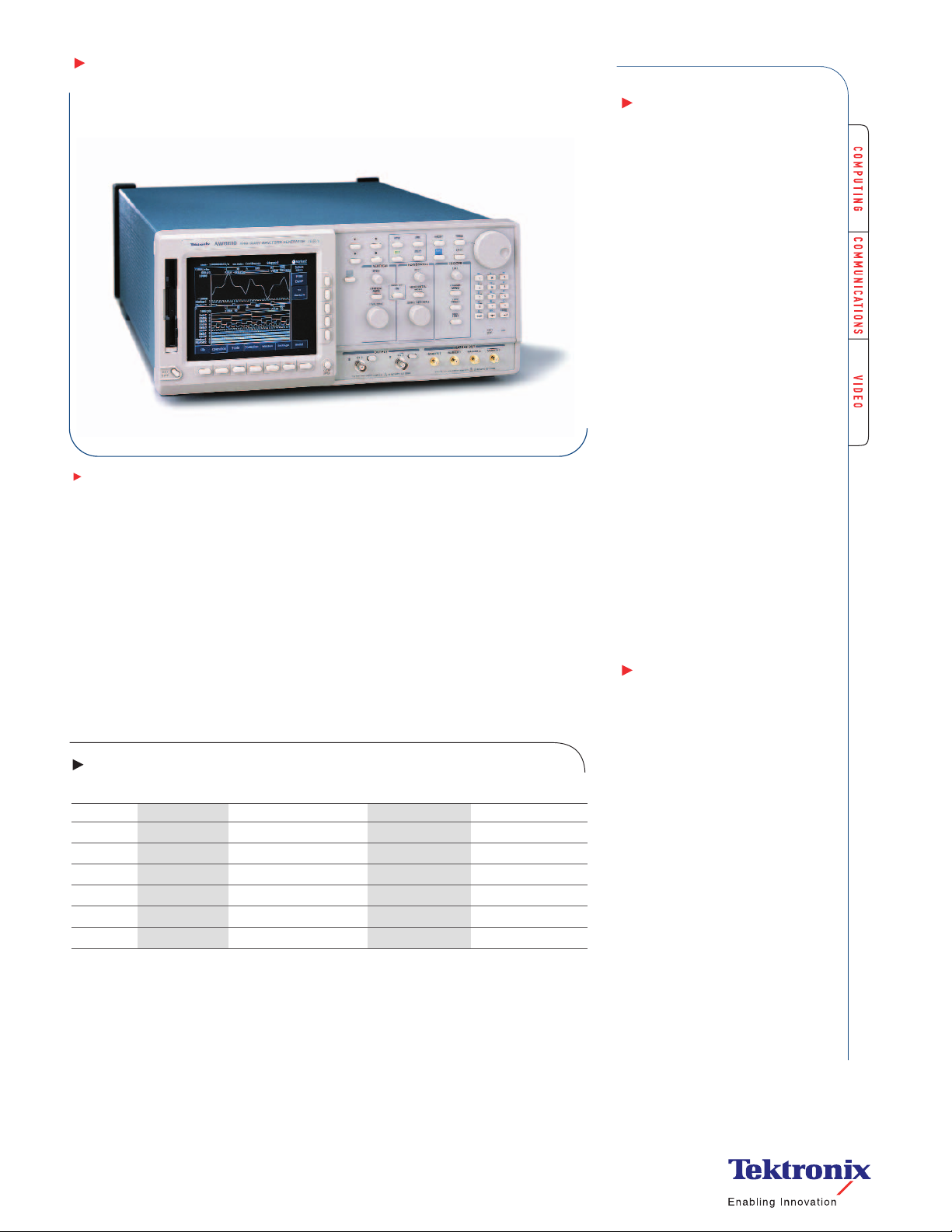
AWG610
AWG610.
AWG610 Combines High Performance with
Ease-of-Use to Tackle Your Challenges in Data
Storage Characterization and Communications
Physical Layer Testing
The AWG10 delivers 2.6 GS/s sample rate
to test high-speed devices and subsystems,
and 8 M points record length for long signal
simulations. Its 8-bit vertical resolution
[Need Title]
ITU-T T1.102 Fibre Channel SDH/Sonet Other
STM1E STS-3 FC1063E OC48/STM16 D2
E5 CEPT STS-1 FC531E OC36 D1
E4 DS4NA FC266E OC24 FDD-1
E3 DS3 FC133E OC18 100Base-TX
E2 DS2 OC12/STM4 Gigabit Ethernet
EI DS1/1C/1A OC3/STM1
provides precise signal replication, while its
400 fs resolution edge shift control allows
greater timing precision.
OC1/STM0
Features & Benefits
2.6 GS/s Sample Rate to
Test High-speed Devices
and Subsystem
1 Analog and 2 Digital
Output Markers to Produce
Complex Mixed Analog and
Digital Signals
8 M Point Record Length
for Long Signal Playtimes
8-bit Vertical Resolution for
Precise Signal Replication
Analog Bandwidth to
Over 800 MHz
EZ Function Generator
Mode Allows Quick Creation
and Edit of Sine, Square,
Triangle, Ramp, Pulse and
DC Waveforms
Waveform Quick Editor with
up to 400 fs Edge Timing
Resolution Delivers Output
Edge Control with Greater
Timing Precision
Real-time Sequencing
Creates Infinite Waveform
Loops, Jumps, Patterns
and Conditional Branches
Built-in Read Channel and
Data Pattern Editing Capability
GPIB and LAN (10Base-T)
Interfaces
Built-in Hard Drive for
Mass Data Storage
Applications
Disk Drive Read/Write
Design and Test
– Head
– Pre-amplifier
– Read/Write
– Servo Test
Communications Design
and Test
– Standard Waveforms
for Communications
Pulse Generation
– Duty Cycle Ranges from
0% to 100% for NRZ Data
–Testing Clock/Gating
Width Variations
Mixed Signal Design and Test
Real-world Simulations
– Corruption and Enhancement
of Ideal Waveforms
–Timing and Amplitude
Signal Impairments
– Jitter Profiles
–Waveforms Imported from
GPIB, Floppy Disk, 10Base-T
Ethernet, DSO or DPO
1
Signal Sources
•
www.tektronix.com/signal_sources
Page 2

Arbitrary Waveform Generator
AWG610
Characteristics
Arbitrary Waveforms
Waveform Length – 512 to 8,100,032 points
in multiples of eight.
Sequence Length – 1 to 8,000 steps.
Sequence Repeat Counter – 1 to 65,536 or infinite.
Function Generator
Waveforms
Operation Mode – Continuous mode only.
Waveform Shape – Sine, Triangle, Square, Ramp,
Pulse, or DC.
Frequency – 1.000 Hz to 260.0 MHz.
Amplitude –
Range: 0.020 V
Resolution: 1 mV.
Offset –
Range: –1.000 V to +1.000 V into 50 Ω.
Resolution: 1 mV.
DC Level –
DC waveform only.
Range: –1.000 V to +1.000 V into 50 Ω.
Resolution: 1 mV.
Polarity – Normal, Invert.
Duty Cycle –
Range: 0.1% to 99.9%, Pulse waveform only.
Resolution:
1.000 Hz to 2.600 MHz: 0.1% step.
2.601 MHz to 13.00 MHz: 0.5% step.
13.01 MHz to 26.00 MHz: 1% step.
26.01 MHz to 52.00 MHz: 2% step.
52.01 MHz to 65.00 MHz: 2.5% step.
65.01 MHz to 104.00 MHz: 4% step.
104.1 MHz to 130.0 MHz: 5% step.
130.1 MHz to 260.0 MHz: 10% step.
Marker Out –
Marker1 Pulse Width:
Hi/Lo: 20%/80% of Period.
Marker2 Pulse Width:
Hi/Lo: 50%/50% of Period, except 65.01 MHz
to 104.0 MHz.
Hi/Lo: 52%/48% of Period, at 65.01 MHz
to 104.0 MHz.
Marker Level:
Hi Level: 2V into 50 Ω.
Lo Level: 0V into 50 Ω.
Clock Generator
Sampling Frequency – 50.000000 kHz to
2.6000000 GHz.
Resolution – 8 digits.
Internal Clock – Accuracy: ±1 ppm.
Phase Noise – (data clock is 1/4th of the output
sample rate).
At 650 MHz, 10 kHz offset: –80 dBc/Hz.
At 650 MHz, 100 kHz offset: –100 dBc/Hz.
p-p
to 2 V
into 50 Ω.
p-p
Operating Modes
Continuous – Waveform is iteratively output. If a
sequence is defined, the sequence order and repeat
functions are applied.
Triggered – Waveform is output only once when
an external, internal, GPIB, LAN or manual trigger
is received.
Gated – Waveform begins output when gate is
true and resets to beginning when false.
Enhanced – Waveform is output as defined by
the sequence.
Internal Trigger Generator
Internal Trigger Rate –
Range: 1.0 µs to 10.0 s.
Resolution: 3 digits, 0.1 µs minimum.
Accuracy: ±0.1%.
Main Output
Output Signal –
Complementary; CH1 and channel/inverse.
Digital to Analog Converter –
Resolution: 8 Bits.
Differential non-linearity: ±1/2-Bit.
Integral non-linearity: ±1-Bit.
Output Connector – Front Panel SMA.
Normal Out
Amplitude –
Output Voltage: –2.0 V to +2.0 V into 50 Ω.
Amplitude: 20 mV to 2.0 V into 50 Ω.
Resolution: 1 mV.
DC Accuracy: ±(1.5% of Amplitude + 2 mV) at
offset = 0 V.
Offset –
Range: –1.000 V to +1.000V into 50 Ω.
Resolution: 1 mV.
Accuracy: ±(1% of offset + 10 mV) at amplitude =
20 mV.
Pulse Response (–1 and 1 waveform data,
0V Offset, Through Filter at 1 V
)–
p-p
Rise Time (10 to 90%): ≤750 ps.
Fall Time (10 to 90%): ≤750 ps.
Aberrations (at 1000 MHz): At 1.0V
p-p
Amplitude: ±10%.
Flatness (after 20 ns from rise/fall edge): ±3%.
Sine Wave Characteristics (2.6 GS/s Clock,
32 Waveform Points, 81.25 MHz Signal
Frequency, 0.5 V Amplitude, 0 V Offset,
Through Filter) –
Harmonics: ≤ –40 dBc, DC to 800 MHz.
Noise: ≤ –50 dBc, DC to 800 MHz.
Phase noise: ≤ –85 dBc/Hz at 10 kHz offset.
Filter
Type – 20, 50, 100, 200 MHz Bessel low-pass.
Rise Time (10 to 90%) –
20 MHz, 17 ns; 50 MHz, 7.0 ns; 100 MHz,3.5 ns;
200 MHz, 1.75 ns.
Delay from Trigger –
20 MHz, 50 ns + 22 clocks; 50 MHz, 40 ns +
22 clocks; 100 MHz, 35 ns + 22 clocks; 200 MHz,
33 ns + 22 clocks; through 30 ns + 22 clocks.
Direct D/A Out
Amplitude
Output Voltage – –0.5 V to +0.5 V into 50 Ω.
Amplitude – 20 mV
p-p
to 1.0 V
into 50 Ω.
p-p
Resolution – 1 mV.
DC Accuracy – ± (2% of Amplitude + 2 mV).
Offset – no function.
DC Offset Accuracy – 0V ±10mV
(waveform data = 0).
Pulse Response (–1 and 1 waveform data,
at 0.5 V
)–
p-p
Rise Time (10 to 90%): ≤400 ps.
Fall Time (10 to 90%): ≤400 ps.
Output Impedance – 50 Ω.
Auxiliary Outputs
Marker
Number – 2 (complementary).
Level –
Hi/Lo: 1.1 V to 3.0V into 50 Ω (Max. 2.5 V
–2.2 V to 6.0 V into 1 MΩ.(Max.5V
Resolution – 0.05 V.
Accuracy – Within ±0.1 V +5% of setting.
Rise/Fall Time (20 to 80%) – 150 ps (2 V
Hi +1 V, Lo –1 V) into 50 Ω.
Variable Delay –
Range: 0 ns to +1.5 ns.
Accuracy: –30% to +10% at 1.5 ms setting.
Resolution: 100 ps.
Marker Skew: 70 ps (typical).
Connector – Front-panel SMA.
10 MHz Reference Clockout –
Amplitude: ≥1V
into 50 Ω. Max 3 V
p-p
Impedance: 50 Ω, AC coupling.
Connector: Rear-panel BNC.
1/4 Clock Out –
Level: ECL 100 K compatible.
Connector: Rear-panel BNC.
Trigger In –
Impedance: 1 kΩ or 50 Ω.
Polarity: POS or NEG.
Input Voltage Range –
1 kΩ:±10V.
50 Ω:±5V.
).
p-p
).
p-p
,
p-p
open.
p-p
2
Signal Sources
•
www.tektronix.com/signal_sources
Page 3

Arbitrary Waveform Generator
AWG610
Threshold –
Level: –5.0 V to 5.0V.
Resolution: 0.1 V.
Accuracy: ±(5% of level + 0.1 V).
Pulse Width (0.2 V amplitude):10 ns minimum.
Trigger Holdoff: ≥576 clocks + 450 ns.
Delay to Marker: 28 ns + 22 clocks.
Delay to Analog Out: (typical).
(filter through).
30 ns + 22 clocks (trigger).
30 ns + 880 clocks (gate).
Connector: Rear-panel BNC.
Event Trig Input –
Number of Events: 4 Bits.
Input Signals: 4 event bits, strobe.
Threshold: TTL level.
Pulse Width: 128 clocks minimum.
Maximum Input: 0 V to +5V (DC + peak AC).
Delay to Analog Out: 850 clocks +20 ns
(ASYNC mode).
Impedance 2.2 kΩ, pull-up to +5 V.
Connector: Rear-panel 9-Pin D-sub.
Reference 10 MHz Clock IN –
Input Voltage Range: 0.2 V to 3.0 V
,
p-p
±10 V maximum.
Impedance: 50 Ω, AC coupled.
Frequency Range: 10 MHz ±0.1 MHz.
Connector: Rear-panel BNC.
General
Characteristics
Display
Area – 13.2 cm (5.2 in.) horizontal by 9.9 cm
(3.9 in.) vertical.
Resolution – 640 horizontal by 480 vertical pixels.
Data Storage
Internal Hard Disk Drive – 3.0 GB (standard).
Floppy Disk Drive – 3.5 in., 1.44 MB.
Option 10 –
Flash Disk replaces HDD, 78 MB. (Opt.10 is best
suited for ATE and system usage requiring 7x24
hour operation.)
Environmental, EMC, Safety
Temperature –
Operating: 10 ºC to +40 ºC.
Nonoperating: –20 ºC to +60 ºC.
Humidity –
Operating: 20 to 80%, noncondensing.
Nonoperating: 5 to 90%, noncondensing.
Altitude –
Operating: Up to 4,500 m. (15,000 ft.).Maximum
operating temperature decreases 1 ºC per 300 m
above 1.5 km.
Nonoperating: Up to 15,000 m (50,000 ft.).
Vibration (Test Limits) –
Operating: 0.27 G
Nonoperating: 2.28 G
10 minutes.
from 5 to 500 Hz, 10 minutes.
RMS
from 5 to 500 Hz,
RMS
Shock (Test Limits) –
Nonoperating: 294 m/s
2
(30 G), half-sine,
11 ms duration.
EMC Compliance –
EN50081-1, EN50082-1.
AS/NZS 20641/2.
Safety – UL3111-1, CSA1010.1, EN61010-1,
IEC61010-1.
Power
Source Power –
Line Voltage Range: 100 to 240 VAC.
Line Frequency: 48 to 63 Hz.
Power Consumption – 600 W at 8 A.
Physical
Characteristics
Dimensions mm in.
Height 193 7.6
Width 422 16.6
Depth 560 22.0
Weight kg lbs.
Net 17 37.5
Other
Programmable Interface –
GPIB: 24-Pin IEEE488.1 connector.
Ethernet: 10Base-T, RJ-45 connector.
Keyboard Connector: 6-Pin mini-DIN connector.
Ordering Information
AWG610
2.6 GS/s, Single-channel arbitrary
waveform generator.
Includes: User manual (071-0554-05), programmer manual (071-0555-01), GPIB programming
examples disk (063-3216-01), sample waveform
library disk (063-3217-00), performance verification
disk (063-3218-00), power cable, fuse
(159-0407-00).
Please specify power plug when ordering.
Recommended Accessories
Service Manual – Order 071-0556-02.
Protective Cover – Order 200-3696-01.
AC Current Probe (Transformer) – 1 GHz:
Order CT1.
AC Current Probe (Transformer)– 200 MHz:
Order CT2.
AC Current Probe (Transformer)– 2 GHz:
Order CT6.
GPIB Cable – Order 012-0991-01.
50 Ω BNC Cable – Order 012-1341-00.
50 Ω BNC Cable – Order 012-1256-00.
50 Ω SMB Cable – Order 012-1458-00.
50 Ω SMB-to-BNC Cable – Order 012-1459-00.
50 Ω BNC Termination – Order 011-0049-01.
50 Ω BNC Power Divider – Order 015-0660-00.
50 Ω SMA Cable (20 inches) – Order
174-1427-00.
50 Ω SMA Cable (1.0 m) – Order 174-1341-00.
50 Ω SMA Cable (60 inches) – Order
174-1428-00.
SMA Precision Cable (1 ns) – Order
015-0562-00.
SMA Precision Cable (2 ns) – Order
015-0560-00.
SMA Precision Cable (5 ns) – Order
015-0561-00.
SMA T Connector – Order 015-1016-00.
50 Ω SMA Termination – Order 015-1022-00.
50 Ω SMA Power Divider – Order 015-1014-00.
SMA(Ma) - BNC(Fe) Connector – Order
015-0554-00.
SMA(Fe) - BNC(Ma) Connector – Order
015-0572-00.
SMA Kit – Order 020-01693-00.
400 MHz BNC Low-pass Filter – Order
015-0659-00.
200 MHz BNC Low-pass Filter – Order
015-0658-00.
100 MHz BNC Low-pass Filter – Order
015-0657-00.
Instrument Cart – Order K420.
Rackmount Conversion Kit – Order
016-1675-01.
Options
Opt. 1O – Flash disk (78 MB) remove HDD and
STBY switch. (Opt. 10 is best suited for ATE and
system usage requiring 7x24 hour operation.)
Opt. 1R – Rackmount.
Power Plug Options
Opt. A0 – US Plug, 115 V, 60 Hz.
Opt. A1 – Euro Plug, 220V, 50 Hz.
Opt. A2 – UK Plug, 240V, 50 Hz.
Opt. A3 – Australian Plug, 240V, 50 Hz.
Opt. A4 – N. American Plug, 240V, 50 Hz.
Opt. A5 – Swiss Plug, 220V, 50 Hz.
Service
Opt. C3 – Calibration Service 3 Years.
Opt. C5 – Calibration Service 5 Years.
Opt. D1 – Calibration Data Report.
Opt. D3 – Calibration Data Report 3 Years
(with Option C3).
Opt. D5 – Calibration Data Report 5 Years
(with Option C5).
Opt. R3 – Repair Service 3 Years.
Opt. R5 – Repair Service 5 Years.
Warranty
One year parts and labor.
Signal Sources
•
www.tektronix.com/signal_sources
3
Page 4

Arbitrary Waveform Generator
AWG610
Contact Tektronix:
ASEAN / Australasia / Pakistan (65) 6356 3900
Austria +43 2236 8092 262
Belgium +32 (2) 715 89 70
Brazil & South America 55 (11) 3741-8360
Canada 1 (800) 661-5625
Central Europe & Greece +43 2236 8092 301
Denmark +45 44 850 700
Finland +358 (9) 4783 400
France & North Africa +33 (0) 1 69 86 80 34
Germany +49 (221) 94 77 400
Hong Kong (852) 2585-6688
India (91) 80-2275577
Italy +39 (02) 25086 1
Japan 81 (3) 3448-3010
Mexico, Central America & Caribbean 52 (55) 56666-333
The Netherlands +31 (0) 23 569 5555
Norway +47 22 07 07 00
People’s Republic of China 86 (10) 6235 1230
Poland +48 (0) 22 521 53 40
Republic of Korea 82 (2) 528-5299
Russia, CIS & The Baltics +358 (9) 4783 400
South Africa +27 11 254 8360
Spain +34 (91) 372 6055
Sweden +46 8 477 6503/4
Taiwan 886 (2) 2722-9622
United Kingdom & Eire +44 (0) 1344 392400
USA 1 (800) 426-2200
USA (Export Sales) 1 (503) 627-1916
For other areas contact Tektronix, Inc. at: 1 (503) 627-7111
Updated 20 September 2002
4
Signal Sources
•
www.tektronix.com/signal_sources
Our most up-to-date product information is available at:
www.tektronix.com
Product Area Assessed: The planning,design/development and manufacture of electronic Test and Measurement instruments.
Product(s) complies with IEEE Standard 488.1-1987, RS-232-C, and
with Tektronix Standard Codes and Formats.
Copyright © 2003,Tektronix, Inc.All rights reserved.Tektronix products are covered
by U.S. and foreign patents, issued and pending. Information in this publication
supersedes that in all previously published material.Specification and price change
privileges reserved. TEKTRONIX and TEK are registered trademarks of Tektronix,
Inc.All other trade names referenced are the service marks,trademarks or registered trademarks of their respective companies.
04/03 HB/SFI 76W-12991-1
 Loading...