

Page 1
Agilent
N5183A MXG Microwave
Analog Signal Generator
Data Sheet
Page 2

Table of Contents
Defini tions ......................................................................................... 3
Frequency .......................................................................................... 4
Amplitude .......................................................................................... 5
Spectral Purity ..................................................................................8
Analog Modula tion .......................................................................... 10
Frequency bands .......................................................................... 10
Frequency modulation .................................................................. 10
Phase modulation ........................................................................ 11
Amplitude modulation .................................................................. 11
Pulse modulation ......................................................................... 12
Narrow pulse modulation ........................................................... 13
Internal analog modulation source ............................................. 14
External modulation inputs .........................................................14
Simultaneous modulation ............................................................ 14
General Characteristics .................................................................. 18
Ordering Information ....................................................................... 18
Archive ............................................................................................ 18
Related Literature ........................................................................... 18
Application literature .................................................................. 18
Product literature ........................................................................ 18
2
Page 3

Definitions
Specification (spec): Represents warranted performance of a calibrated instrument
that has been stored for a minimum of 2 hours within the operating temperature range
of 0 to 55 °C, unless otherwise stated, and after a 45 minute warm-up period. The
specifications include measurement uncertainty. Data represented in this document
are specifications unless otherwise noted.
Typical (typ): Represents characteristic performance, which 80% of the instruments
manufactured will meet. This data is not warranted, does not include measurement
uncertainty, and is valid only at room temperature (approximately 25 °C).
Nominal (nom): The expected mean or average performance, or an attribute whose
performance is by design, such as the 50 Ω connector. This data is not warranted and
is measured at room temperature (approximately 25 °C).
Measured (meas): An attribute measured during the design phase for purposes of
communicating expected performance, such as amplitude drift vs. time. This data is
not warranted and is measured at room temperature (approximately 25 °C).
Note: All graphs contain measured data from several units at room temperature unless
otherwise noted.
3
Page 4

Frequency
Range
Option 520 100 kHz to 20 GHz
Option 532 100 kHz to 31.8 GHz
Option 540 100 kHz to 40 GHz
Minimum frequency 100 kHz
1
Resolution 0.01 Hz
Phase offset Adjustable in nominal 0.01° increments
Frequency switching speed
2, 3
Type Standard Option UNZ
SCPI mode ≤ 5 ms ≤ 1.15 ms, 750 µs (typ)
List/Step sweep mode ≤ 5 ms ≤ 900 µs, 600 µs (typ)
Stability ± aging rate
± temperature effects
± line voltage effects
Internal time base < ±1 ppm/yr
reference oscillator
aging rate
Tempera ture e f fec ts
± 1 ppm (typ) (0 to 55 °C)
Line voltage effects ± 0.1 ppm (nom)
Line voltage range 5% to –10% (nom)
Reference output
Frequency 10 MHz
Amplitude ≥ +4 dBm (nom) into 50 Ω load
External reference input
Fixed Variable (Option 1ER)
Input frequency 10 MHz 1 to 50 MHz
Lock range ± 10 Hz
Amplitude > –3.5 to 20 dBm (nom)
Impedance 50 Ω (nom)
Digital sweep
Operating modes Step sweep (equally or logarithmically spaced
frequency steps)
List sweep (arbitrary list of frequency steps)
Can also simultaneously sweep amplitude. See
amplitude section for more detail.
Sweep range Within instrument frequency range
Dwell time 100 μs to 100 s
Number of points 2 to 65535 (step sweep)
1 to 1601 (list sweep)
Step change Linear or logarithmic
Triggering Free run, trigger key, external, timer, bus (GPIB, LAN, USB)
Markers In step sweep mode, create up to 20 frequency markers
Display Z-axis or RF amplitude pulse
Functions M1 to center, M1/M2 to start/stop, marker delta
1. Per formance below 2 50 kHz is unspecified , except as indicated.
2. Time f rom receipt of SCPI command or t rigger signal to within 0.1 ppm of final frequency or w ithin
100 Hz, whichever is gr eater, and amplitude set tle d to within 0.2 dB.
3. Specification does not apply when switching to or from frequencies < 50 0 kHz, when ALC level is
< –5 dBm for Op tion 5 40 or < 0 dBm for Option 520, or when frequency crosses 0 .002, 0 .02 , 0.1, 2. 0, 3. 2,
20.0, 25.6, or 32.0 GHz.
4
Page 5
Amplitude
Maximum output power
1
Range Standard2 Option 1EA3
Option 520
100 to 250 kHz +11 +14
> 250 kHz to 3.2 GHz +11 +15
> 3.2 to 20 GHz +11 +18
Options 532 and 540
100 to 250 kHz +11 +14
250 kHz to 3.2 GHz +7 +14
> 3.2 to 17 GHz +7 +15
> 17 to 31.8 GHz +7 +13
> 31.8 to 40 GHz +7 +12
Minimum output power
Standard –20 dBm
Option 1E1 –90 dBm
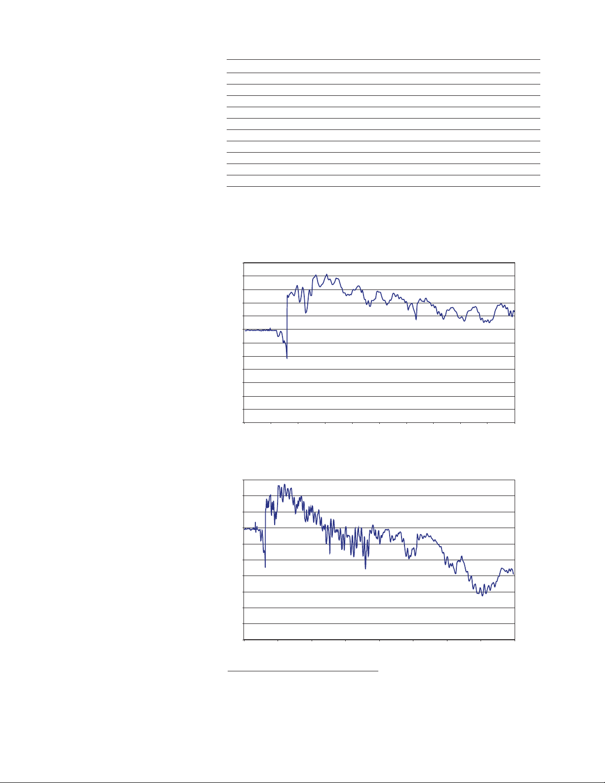
Maximum available power Option 520 with Option 1EA (measured)
27
26
25
24
23
22
21
20
Amplitude (dBm)
19
18
17
16
15
0 2000 4000 6000 8000 10000 12000 14000 20000
4
Frequency (MHz)
16000 18000
Maximum available power Option 540 with Option 1EA (measured)
25
24
23
22
21
20
19
Amplitude (dBm)
18
17
16
15
0 5000 10000 15000 20000 25000 30000 35000 40000
Frequency (MHz)
1. Quo ted specif ications between 15 and 35 °C . Max imum outpu t power typically decreases by 0. 2 dB/ °C
for temperatures outside this range.
2. Settable power +2 dB higher than specified.
3. Set table power +30 dBm.
4.
Settable to –130 dBm.
5
Page 6
Resolution 0.01 dB
Step attenuator 0 to 115 dB in 5 dB steps
(Option 1E1)
Amplitude
–15 to maximum specified output power with step attenuator
hold range in 0 dB. Can be offset using Option 1E1 mechanical attenuator.
Amplitude switching speed
1, 2
Type
SCPI mode 2 ms (typ)
List/Step sweep mode 2 ms (typ)
Absolute level accuracy [dB]
3, 4
Frequency range –20 to < –10 dBm –10 to +10 dBm > +10 dBm
250 kHz to 2 GHz ±1.4 ±0.6 ±0.6
2 to 20 GHz ±1.3 ±0.9 ±0.9
20 to 40 GHz ±1.3 ±0.9 ±1.0
Absolute level accuracy with Option 1E1 (dB)
4
Frequency range –90 to < –75 dBm –75 to < –10 dBm –10 to +10 dBm > +10 dBm
250 kHz to 2 GHz ±1.4 ±0.7 ±0.6 ±0.6
2 to 20 GHz ±1.6 ±1.0 ±0.9 ±0.9
20 to 40 GHz ±2.0 ±1.1 ±0.9 ±1.0
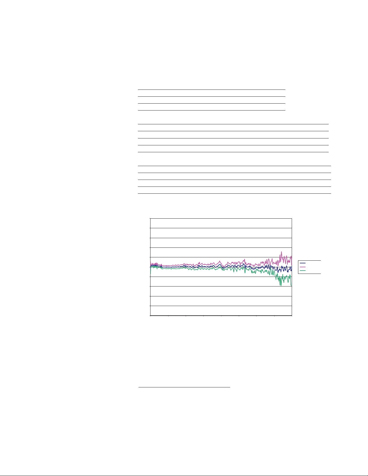
Measured level accuracy Options 520 & 540 at –90 dBm
1
0.8
0.6
0.4
0.2
0
–0.2
Level accuracy (dB)
–0.4
–0.6
–0.8
–1
0 5000 10000 15000 20000 25000 30000 35000 40000
Frequency (MHz)
mean
+STD Dev
–STD Dev
1. Time from r eceipt of SCPI command or trigger signal to amplitude se ttled wi thin 0 .2 dB .
2. Specific ation does not apply when switching from and to amplitudes where A LC levels ar e < –5 dBm
for Option 5 40 or < 0 dBm for O ption 520.
3. Level accuracy applie s from –20 dBm to ma ximum output power bet ween 15 °C and 3 5 °C.
4. For temper atures outside this r ange, absolute le vel accuracy degr ades by 0.01 dB/degree C for
frequencies ≤ 4. 5 GHz an d 0.0 2 dB/degr ee C for f requencies > 4.5 GHz.
connector s (Option 1ED), speci fications are degrade d typically 0. 2 dB above 18 GHz. Specifications
do not apply above the maximum specified power.
For ins trument s wit h Type-N
6
Page 7

Temperature stability 0.01 dB/°C (typ) for temperatures < 20 °C or > 30 °C
User flatness correction
Number of points 2 to 1601
Number of tables 10000 maximum; dependent on available free memory in
instrument
Entry modes USB/L AN direct power meter control, LAN to GPIB and
USB to GPIB, remote bus and manual USB/GPIB power
meter control
SWR 100 kHz to 20 GHz 1.6:1 (typ)
> 20 to 40 GHz 1.8:1 (typ)
Leveling modes Internal, external detector, ALC off, search
External detector leveling
1
Range –0.2 mV to –0.5V (nom)
Bandwidth 10 kHz (typ)
Digital sweep modes
Operating modes Step sweep (evenly spaced amplitude steps)
List sweep (arbitrary list of amplitude steps)
Can also simultaneously sweep frequency. See frequency
section for more detail.
Sweep range Within instrument amplitude range
Dwell time 100 μs to 100 s
Number of points 2 to 65535 (step sweep)
1 to 1601 (list sweep)
Step change Linear
Triggering Free run, trigger key, external, timer, bus (GPIB, LAN, USB)
1. Not intended for pulsed operation.
7
Page 8

Spectral Purity
–
–
–
–
–
–
–
–
–
–
–
–
–
–
–
–
Single sideband phase noise (at 20 kHz offset from carrier)
Frequency range dBc/Hz dBc/Hz (typ)
250 kHz to < 250 MHz –113 –116
250 to < 375 MHz –125 –128
375 to < 750 MHz –119 –122
750 MHz to < 1.5 GHz –113 –116
1.5 to < 3.0 GHz –107 –110
3.0 to < 6.0 GHz –101 –104
6.0 to < 12.0 GHz –95 –98
12.0 to < 24.0 GHz –89 –92
24.0 to 40.0 GHz –83 –86
SSB Phase Noise
0
–10
–20
–30
–40
–50
–60
–70
–80
–90
100
110
120
130
140
150
160
170
10 100 1000 10000 100000 1000000 1E+07 1E+08
L(f) [dBc/Hz] vs. f [Hz]
40 GHz
20 GHz
10 GHz
1 GHz
AM noise at 10 GHz
–20
–30
–40
–50
–60
–70
–80
–90
100
110
120
130
140
150
160
170
10 100 1000 10000 100000 1000000 1E+07 1E+08
8
M(f) (dBc/Hz) vs. f(Hz)
Page 9

Residual FM (CW mode, 0.3 to 3 kHz bandwidth, CITT, RMS)
< N*5Hz (typ)
Broadband noise CW mode at +10 dBm or maximum specified output
power, whichever is lower for offsets > 10 MHz
0.25 to 10 GHz –145 dBc/Hz (typ)
10 to 20 GHz –135 dBc/Hz (typ)
20 to 40 GHz –130 dBc/Hz (typ)
1
Harmonics (dBc)
250 kHz to 2 GHz –28 (–30 typ)
> 2 to 20 GHz –54 (– 60 typ)
> 20 to 40 GHz –56 (typ)
Non-harmonics (dBc)
1, 2
250 kHz to 250 MHz –62 (–89 typ)
> 250 to 375 MHz – 68 (– 86 typ)
> 375 to 750 MHz – 57 (–74 typ)
> 750 MHz to 1.5 GHz –54 (–70 typ)
> 1.5 to 3.2 GHz – 54 (–68 typ)
> 3.2 to 6 GHz –47 (– 63 typ)
> 6 to 12 GHz – 41 (–57 typ)
> 12 to 24 GHz (–50 typ)
> 24 to 40 GHz (– 45 typ)
Subharmonics (dBc)
1
250 kHz to 1.5 GHz None
> 1.5 GHz to 20 GHz –53
> 20 to 40 GHz –50
1. CW mode at +10 dBm or maximum specified output p ower, w hichever is lower.
2. Non-harmonics specifications apply to units with serial numbers ending with 49060000 or greater.
For uni ts with lower serial numbers, ref er to the archive section at the end of this document .
9
Page 10

Analog Modulation
Frequency bands1
Frequency N
100 kHz to < 250 MHz 1
250 to < 375 MHz 0.250
375 to < 750 MHz 0.500
750 to < 1.5 GHz 1
1.5 to < 3.0 GHZ 2
3.0 to < 6.0 GHz 4
6.0 to < 12.0 GHz 8
12.0 to < 24.0 GHz 16
24.0 to 40 GHz 32
Frequency modulation
(Option UNT)
Maximum deviation N x 10 MHz (nom)
Resolution 0.1% of deviation or 1 Hz, whichever is
greater (nom)
Deviation accuracy
1 kHz rate, deviation is N x 50 kHz
Modulation frequency response (at 100 kHz deviation)
DC coupled DC to 3 MHz (nom) DC to 7 MHz (nom)
AC coupled 5 Hz to 3 MHz (nom) 5 Hz to 7 MHz (nom)
< ± 2% + 20 Hz
1 dB bandwidth 3 dB bandwidth
Carrier frequency accuracy < ±0.2% of set deviation + (N x 1 Hz)
2
relative to CW in DCFM < ±0.06% of set deviation + (N x 1 Hz) (typ)
Distortion < 0.4%
1 kHz rate, deviation is N x 50 kHz
Sensitivity when using
external input
+1V peak for indicated deviation (nom)
3
1. N is a factor used to help def ine frequency and phase modulation specifications within the document.
2. Specific ation valid for temperature changes of less than ± 5° C since last DCFM c alibration.
3. Typical perf ormance immediately afte r a DCFM calib ration.
10
Page 11

Phase modulation
(Option UNT)
Modulation deviation and frequency response:
Max deviation 3 dB bandwidth
Nominal bandwidth N x 5 radians (nom) DC to 1 MHz (nom)
High bandwidth mode N x 0.5 radians (nom) DC to 4 MHz (nom)
Resolution
0.1% of deviation
Deviation accuracy
< +0.5% + 0.01 rad (typ)
1 kHz rate, normal bandwidth mode
Distortion < 0.2% (typ)
1 kHz rate, deviation normal bandwidth mode
Sensitivity when using
external input +1V peak for
Amplitude modulation
1
indicated deviation (nom)
(Option UNT)
AM Depth Linear Exponential
Maximum settable 90% 20 dB
Resolution 0.1% of depth (nom) 0.01 dB (nom)
Accuracy (1 kHz rate) < ±4% of setting <±(4% of setting
+ 1% (typ) + 0.2 dB) (typ)
Modulation rate (3 dB bandwidth, 30% depth)
DC coupled 0 to 10 kHz (typ)
AC coupled 5 Hz to 10 kHz (typ)
Distortion (1 kHz rate, 30% depth) < 2.0% (typ)
Sensitivity when using
external input +1V peak for indicated depth (nom)
1. AM is speci fied at carrier frequencies > 2 MHz, ALC on, and w hen A M envelope does not exceed max
power or go below –15 dBm for Option 52 0 or –2 0 dBm for Option 540.
11
Page 12

Pulse modulation
1
(Option UNU)
On/Off ratio > 80 dB (typ)
2
Rise time < 50 ns (typ)
Fall time < 50 ns (typ)
Minimum width
ALC on ≥ 2 μs (typ)
ALC off ≥ 500 ns (typ)
Resolution 20 ns (nom)
Pulse repetition frequency
ALC on DC to 500 kHz
ALC off DC to 2 MHz
Level accuracy < 1 dB (typ)
(relative to CW, ALC on or off)
Video feedthrough < 350 mV (typ)
Pulse overshoot < 15% (nom)
Pulse compression 15 ns (typ)
Pulse delay
RF delay (video to RF output) 10 ns (nom)
Video delay (ext input to video) 30 ns (nom)
External input
Input impedance 50 ohm (nom)
Level +1 Vpeak = ON (nom)
Internal pulse generator
Modes Free-run, square, triggered, adjustable doublet,
trigger doublet, gated, and external pulse
Square wave rate 0.1 Hz to 10 MHz, 0.1 Hz resolution (nom)
Pulse period 500 ns to 42 seconds (nom)
Pulse width 500 ns to pulse period – 10 ns (nom)
Resolution 10 ns (nom)
Adjustable trigger delay – pulse period + 10 ns to pulse period to pulse
width –10 ns
Settable delay Free run –3.99 to 3.97 μs
Triggered 0 to 40 s
Resolution 10 ns (nom)
(delay, width, period)
Pulse doublets
1st pulse delay 0 to 42 s – pulse width – 10 ns
(relative to sync out)
1st pulse width 500 ns to 42 s – delay – 10 ns
2nd pulse delay 0 to 42 s – (delay1 + width
2
) – 10 ns
(relative to pulse 1)
2nd pulse width 20 ns to 42 s – (delay1 + delay
2
) – 10 ns
1. Pulse specifications apply to frequencies > 500 M Hz. O perable down to 10 MH z.
2. A pplies to power levels > – 5 dBm for Opt ion 1E1.
12
Page 13

Narrow pulse modulation
Sync
Output
Video
Output
RF Pulse
Output
T
d
T
m
T
w
T
rf
V
f
T
f
T
r
V
or
T
p
50%
50%
10%
90%
50%
1
(Option UNW)
500 MHz to 3.2 GHz Above 3.2 GHz
On/Of f ratio > 80 dB (typ) > 80 dB (typ)
Rise/Fall times (Tr, Tf) < 10 ns (7 ns) < 10 ns (7 ns)
Minimum pulse width
Internally leveled ≥ 2 us ≥ 2 us
ALC off
2
≥ 20 ns ≥ 20 ns
Repetition frequency
Internally leveled 10 Hz to 500 kHz 10 Hz to 500 kHz
ALC off
2
DC to 5 MHz DC to 10 MHz
Level accuracy relative to CW
Internally leveled < ±1.0 dB (typ) < ±1.0 dB (typ)
ALC off
2
±1.0 dB (typ) ±1.0 dB (t y p)
Width compression < 5 ns (typ) < 10 ns (typ)
RF width relative to video out
Video feed-through
3
< 300 mV (typ) < 10 mV (typ)
Video delay - 30 ns (nom) 30 ns (nom)
ext input to video
RF delay -video to 10 ns (nom) 20 ns (nom)
RF output
Pulse overshoot < 15% (nom) < 15% (nom)
Input level +1 Vpeak = RF On +1 Vpeak = RF On
Input impedance 50 Ω (nom) 50 Ω (nom)
Td Video delay (variable)
Tw Video pulse width
(variable)
Tp Pulse period (variable)
Tm RF delay
Trf RF pulse width
Tf RF pulse fall time
Tr RF pulse rise time
Vor Pulse overshoot
Vf Video feedthrough
1. Pulse specifications apply to frequencies > 500 M Hz. O perable down to 10 MH z.
2. With power search on.
3. A pplies to power levels < +10 dBm .
13
Page 14

Internal analog modulation source
(Option UNT)
Waveform Sine
Rate range 0.1 Hz to 2 MHz (tunable to 3 MHz)
Resolution 0.1 Hz
Frequency accuracy Same as RF reference source (nom)
External modulation inputs
(Requires Option UNT)
Modulation types FM, AM, phase mod, pulse mod
Input impedance 50 Ω (nom)
Simultaneous modulation
All modulation types (FM, AM, φM and pulse modulation) may be simultaneously
enabled except: FM and phase modulation can not be combined; two modulation types
can not be simultaneously generated using the same modulation source. For example,
AM and FM can run concurrently and will modulate the output RF. This is useful for
simulating signal impairments.
1
1. If AM or pulse modulation are on, then phase and FM specif ications do not apply.
14
Page 15

General Characteristics
Remote programming
Interfaces GPIB IEEE-488.2, 1987 with listen and talk
LAN 100BaseT LAN interface, LXI class C
compliant
USB Version 2.0
Control languages SCPI Version 1997.0
Compatibility languages supporting a subset of common commands
Agilent Technologies 8360 series, E8247C, E8257C, E8257D, E8241A,
E8244A, E8251A, E8254A, E4428C, E4438C,
E8267C/D, 8662A, 8663A , 83711B, 83712B,
83731B, 83732B, 83751B, 83752B, 8340B,
8341B
Power requirements 100 to 120 VAC, 50 to 60 Hz and 400 Hz
220 to 240 VAC, 50 to 60 Hz
250 W maximum
Operating temperature range 0 to 55 °C
Storage temperature range –40 to 70 °C
Operating and storage altitude 15,000 feet
Environmental stress Samples of this product have been type tested in
accordance with the Agilent Environmental Test
Manual and verified to be robust against the
environmental stresses of Storage, Transportation
and End-use; those stresses include but are not
limited to temperature, humidity, shock, vibration,
altitude and power line conditions. Test Methods
are aligned with IEC 60068-2 and levels are
similar to MIL-PRF-28800F Class 3.
Safety Complies with European Low Voltage Directive
73/23/EEC, amended by 93/68/EEC
• IEC/EN 61010-1
• Canada: CSA C22.2 No. 61010-1
• USA: UL 61010-1
EMC Complies with European E MC Directive 89/336/
EEC, amended by 93/68/EEC
• IEC/EN 61326
• CISPR Pub 11 Group 1, class A
• AS/NZS CISPR 11:2002
• ICES/NMB-001
Memory Memory is shared by instrument states, sweep list
files, and other files. There is 512 MB of flash
memory available in the N5181A MXG. Depending
on how the memory is utilized, a maximum of
1000 instrument states can be saved.
15
Page 16

Security (Option 006) Memory sanitizing, memory sanitizing on power
on, and display blanking.
Self test Internal diagnostic routines test most modules
in a preset condition. For each module, if its
node voltages are within acceptable limits, the
module “passes” the test.
Weight ≤ 13.8 kg (30 lb.) net,
≤ 28.4 kg (62 lb.) shipping
Dimensions 103 mm H x 426 mm W x 432 mm L
(4.07 in H x 16.8 in W x 17 in L)
Recommended calibration cycle 24 months
ISO compliant The Agilent N5181A MXG is manufactured in an
ISO-9001 registered facility in concurrence with
Agilent Technologies’ commitment to quality.
Front panel connectors
1
RF output Output impedance 50 Ω (nom)
Option 520 Precision APC-3.5 male, or Type-N with
Option 1ED
Option 532/540 Precision 2.4 mm male; plus 2.4 – 2.4 mm and
2.4 – 2.9 mm female adapters
Maximum reverse power 0.5 W, 0 Vdc
USB 2.0 Used with a memory stick for transferring
instrument states, licenses and other files into
or out of the instrument. Also used with U2000
series USB average power sensors. For a
current list of supported memory sticks, visit
www.agilent.com/find/MXG, click on Technical
Support, and refer to FAQs: WaveformDownloads
and Storage.
Rear panel connectors
1
RF output Outputs the RF signal via a precision N type
(Option 1EM) female connector.
Sweep out Generates output voltage, 0 to +10 V when the
signal generator is sweeping. This output can
also be programmed to indicate when the source
is settled or output pulse video and is T TL and
CMOS compatible in this mode. Output
impedance < 1 Ω, can drive 2k Ω. Damage
levels are ±15 V.
AM External AM input. Nominal input impedance is
50 Ω. Damage levels are ±5 V.
FM External FM input. Nominal input impedance is
50 Ω. Damage levels are ±5 V.
Pulse External pulse modulation input. This input is
TTL and CMOS compatible. Low logic levels are
0 V and high logic levels are +1 V. Nominal input
impedance is 50 Ω. Input damage levels are
≤ –0.3 V and ≥ +5.3 V.
1. All connec tors are BNC unless otherw ise noted.
16
Page 17

Trigger in This high impedance input accepts TTL and
CMOS level signals for triggering point-to-point
in sweep mode. Damage levels are ≤ –0.3 V and
≥ +5.3 V.
Trigger out Outputs a T TL and CMOS compatible level
signal for use with sweep mode. The signal is
high at start of dwell, or when waiting for point
trigger in manual sweep mode; low when dwell
is over or point trigger is received. This output
can also be programmed to indicate when the
source is settled, pulse synchronization, or pulse
video. Nominal output impedance is 50 ohms.
Input damage levels are ≤ –0.3 V and ≥ +5.3 V.
Reference input Accepts a 10 MHz reference signal used to
frequency lock the internal timebase. Option 1ER
adds the capability to lock to a frequency from
1 MHz to 50 MHz. Nominal input level –3.5 to
+20 dBm, impedance 50 Ω.
10 MHz out Outputs the 10 MHz reference signal used by
internal time base. Level is nominally +3.9 dBm.
Nominal output impedance 50 Ω. Input damage
level is +16 dBm.
USB 2.0 The USB connector provides remote programming
functions via SCPI.
LAN (100 BaseT) The LAN connector provides the same SCPI
remote programming functionality as the GPIB
connector. The L AN connector is also used to
access the internal web server and FTP server.
The LAN supports DHCP, sockets SCPI, VXI-11
SCPI, connection monitoring, dynamic host name
services, TCP keep alive. This interface is L XI
class C compliant.
GPIB The GPIB connector provides remote
programming functionality via SCPI.
ALC input This female BNC connector is used for negative
external detector leveling.
Input impedance 100 kΩ (nominal)
Signal levels –0.2 mV to –0.5 V
Damage levels ≤ –12 V and ≥ 1 V
Z-axis output This female BNC connector supplies a +5 V
(nominal) level during retrace and band switch
intervals of a step or list sweep. During step or
list sweep, this connector supplies a –5 V
(nominal) level when the RF frequency is at a
marker frequency and intensity marker mode is
on. The load impedance should be ≥ 5 kΩ.
17
Page 18

Ordering Information
N5183A MXG microwave analog signal generator
Frequency
520 Frequency range from 100 kHz to 20 GHz
532 Frequency range from 100 kHz to 31.8 GHz
540 Frequency range from 100 kHz to 40 GHz
Performance enhancements
UNZ Fast frequency switching
1E1 Step attenuator
1EA High power
UNU Pulse modulation
UNW Narrow pulse modulation
UNT AM, FM, phase modulation
006 Instrument security
1ER Flexible reference input (1-50 MHz)
1EM Move RF output to rear panel
1ED Type N RF output connector
Accessories
1CM Rackmount kit
1CN Front handle kit
1CP Rackmount and front handle kit
1CR Rack slide kit
AX T Transit case
Archive
Related Literature
Non-harmonics (dBc)
(For serial numbers < 49060000)
250 kHz to 250 MHz –54 (–89 typ)
> 250 to 375 MHz –61 (– 86 typ)
> 375 to 750 MHz –55 (–74 typ)
> 750 MHz to 1.5 GHz –48 (–70 typ)
> 1.5 to 3.2 GHz – 47 (–68 typ)
> 3.2 to 6 GHz –40 (– 63 typ)
> 6 to 12 GHz –33 (–57 typ)
> 12 to 24 GHz – 50 (typ)
> 24 to 40 GHz –45 (typ)
Application literature
RF Source Basics, a self-paced tutorial (CD-ROM), literature number 5980-2060E
Product literature
Agilent MXG Signal Generator, Configuration Guide, literature number 5989-5485EN
See the Agilent M XG web page for the latest information. Get the latest news, product
and suppor t information, application literature, firmware upgrades and more at
www.agilent.com/find/MXG
18
Page 19

www.agilent.com
Agilent Email Updates
www.agilent.com/find/emailupdates
Get the latest information on the
products and applications you select.
www.lxistandard.org
LXI is the LAN-based successor to
GPIB, providing faster, more efficient
connectivity. Agilent is a founding
member of the LXI consortium.
Agilent Channel Partners
www.agilent.com/find/channelpartners
Get the best of both worlds: Agilent’s
measurement expertise and product
breadth, combined with channel
partner convenience.
Remove all doubt
Our repair and calibration services will
get your equipment back to you, performing like new, when promised. You
will get full value out of your Agilent
equipment through-out its lifetime.
Your equipment will be serviced by
Agilent-trained technicians using the
latest factory calibration procedures,
automated repair diagnostics and genuine parts. You will always have the utmost confidence in your measurements.
For information regarding self maintenance of this product, please contact
your Agilent office.
Agilent offers a wide range of additional expert test and measurement
services for your equipment, including
initial start-up assistance, onsite education and training, as well as design,
system integration, and project management.
For more information on repair and
calibration services, go to:
www.agilent.com/find/removealldoubt
For more information on Agilent
Technologies’ products, applications or
services, please contact your local Agilent
office. The complete list is available at:
www.agilent.com/fi nd/contactus
Americas
Canada (877) 894 4414
Latin America 305 269 7500
United States (800) 829 4444
Asia Pacifi c
Australia 1 800 629 485
China 800 810 0189
Hong Kong 800 938 693
India 1 800 112 929
Japan 0120 (421) 345
Korea 080 769 0800
Malaysia 1 800 888 848
Singapore 1 800 375 8100
Taiwan 0800 047 866
Thailand 1 800 226 008
Europe & Middle East
Austria 43 (0) 1 360 277 1571
Belgium 32 (0) 2 404 93 40
Denmark 45 70 13 15 15
Finland 358 (0) 10 855 2100
France 0825 010 700*
*0.125 €/minute
Germany 49 (0) 7031 464 6333
Ireland 1890 924 204
Israel 972-3-9288-504/544
Italy 39 02 92 60 8484
Netherlands 31 (0) 20 547 2111
Spain 34 (91) 631 3300
Sweden 0200-88 22 55
Switzerland 0800 80 53 53
United Kingdom 44 (0) 118 9276201
Other European Countries:
www.agilent.com/fi nd/contactus
Revised: October 1, 2009
Product specifications and descriptions
in this document subject to change
without notice.
© Agilent Technologies, Inc. 2008, 2010
Printed in USA, February 23, 2010
5989-7572EN
 Loading...