

Page 1
EXG X-Series Signal Generator
N5173B Microwave Analog
9 kHz to 13, 20, 31.8, or 40 GHz
Data Sheet
Page 2

Table of Contents
Definitions .........................................................2
Frequency specifications ..............................................3
Amplitude specifications ..............................................5
Spectral purity specifications ..........................................8
Analog modulation specifications ......................................12
General characteristics ..............................................16
Inputs and outputs ..................................................18
Related literature ...................................................20
Definitions
Specification (spec): Specifications represent warranted performance of a
calibrated instrument that has been stored for a minimum of 2 hours within the
operating temperature range of 0 to 55 °C, unless otherwise stated, and after a
45 minute warm-up period. The specifications include measurement uncertainty.
Data represented in this document are specifications unless otherwise noted.
Typical (typ): Typical (typ) describes additional product performance
information that is not covered by the product warranty. It is performance beyond
specifications that 80 percent of the units exhibit with a 95 percent confidence
level at room temperature (approximately 25 °C). Typical performance does not
include measurement uncertainty.
Nominal (nom) or measured (meas): Nominal (nom) or measured (meas)
describes a performance attribute that is by design or measured during the design
phase for the purpose of communicating sampled, mean or average performance,
such as the 50 ohm connector or amplitude drift vs. time. This data is not
warranted and is measured at room temperature (approximately 25 °C).
2
Page 3

Frequency Specifications
Range
Frequency range Option 513 9 kHz to 13 GHz
Option 520 9 kHz to 20 GHz
Option 532 9 kHz to 31.8 GHz
Option 540 9 kHz to 40 GHz
Resolution 0.001 Hz (nom)
Phase offset Adjustable in nominal 0.1° increments
Frequency switching speed 1 () = typical
Standard Option UNZ
CW mode
SCPI mode (≤ 5 ms) ≤ 1.15 ms (≤ 750 µs) < 1.65 ms (1 ms)
List/step sweep mode (≤ 5 ms) ≤ 900 µs (≤ 600 µs) < 1.4 ms (850 µs)
1. Time from receipt of SCPI command or trigger signal to within 0.1 ppm of final frequency or within 100 Hz, whichever is greater.
2. For export control purposes CW switching speed to within 0.05% of final frequency is 190 us (meas).
3. For export control purposes CW switching speed to within 0.05% of final frequency is > 400 us (nom) below 20 GHz and > 600 us (nom) above 20 GHz.
4. Specifications apply when status register updates are off.
2, 4
Option UZ2,
3, 4
3
Page 4

Frequency reference
Accuracy
± aging rate
± temperature effects
± line voltage effects
± initial setting accuracy
Internal time base reference oscillator aging rate
1
< ± 1 x 10^-7/year (nom)
< ± 5 x 10^-10/day after 30 days (nom)
Initial achievable calibration accuracy ± 4 x 10^-8 or ± 40 ppb
Adjustment resolution < 1 x 10^-10 (nom)
Temperature effects < ± 2 x 10^-8 from 20 to 30 °C (nom)
Line voltage effects < ± 1 x 10^-9 for ± 10% change (nom)
Reference output
Frequency 10 MHz
Amplitude ≥ +4 dBm, (nom) into 50 Ω load
External reference input
Input frequency standard 10 MHz
Input frequency Option 1ER 1 to 50 MHz (in multiples of 0.1 Hz)
Lock range ± 1 ppm (nom)
Amplitude 5 dBm ± 2 dB (nom)
2
Impedance 50 Ω (nom)
Waveform Sine or square
Sweep modes (frequency and amplitude)
Operating modes Step sweep (equally spaced frequency and amplitude or
logarithmically spaced frequency steps)
List sweep (arbitrary list of frequency and amplitude steps)
Simultaneously sweep waveforms with N5182B; see baseband
generator section for more detail
Sweep range Within instrument frequency range
Dwell time 100 µs to 100s
Number of points 2 to 65535 (step sweep)
1 to 3201 (list sweep)
Step change Linear or logarithmic
Triggering Free run, trigger key, external, timer, bus (GPIB, LAN, USB)
1. Aging rate is determined by design as a function of the OCXO.
2. Inputs between +3 dBm to +20 dBm are allowed.
4
Page 5
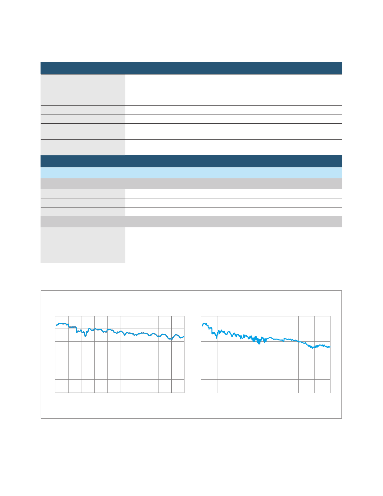
Amplitude Specifications
0
5
10
15
20
25
30
02468101214161820
Maximum power
Options 513/520 with Option 1EA and 1E1 (CW rms, measured)
Frequency (GHz) vs. amplitude (dBm)
0
5
10
15
20
25
30
0510 15 20 25 30 35 40
Maximum power
Options 532/540 with Option 1EA and 1E1 (CW rms, measured)
Frequency (GHz) vs. amplitude (dBm)
Output parameters
Settable range
(with Option 1E1 and 1EA)
Settable range
(without Option 1E1 and 1EA)
Resolution 0.01 dB, (nom)
Step attenuator (1E1) 0 to 115 dB in 10 dB steps mechanical type
Attenuator hold range –15 dBm to maximum specified output power with step attenuator in 0 dB state; can be offset
Connector 513/520 = 3.5 SMA male, 532/540 = 2.4 mm male, 50 Ω (nom)
Max output power
1
(dBm, with or without step attenuator, Option 1E1)
Frequency Standard High power Option 1EA
Option 513, 520
9 kHz to 3.2 GHz +18 +23
> 3.2 to 13 GHz +18 +20
> 13 to 20 GHz +15 +19
Option 532, 540
9 kHz to 3.2 GHz +14 +21
> 3.2 to 17 GHz +14 +16
> 17 to 31.8 GHz +13 +15
> 31.8 to 40 GHz +11 +15
1. Quoted specifications between 15 and 35 °C. Maximum output power typically decreases by 0.05 dB/°C for temperatures outside this range.
+30 to –130 dBm
+19 to –20 dBm
using option 1E1 mechanical attenuator
(Option 1ED adds Type-N connector to a 513 or 520)
5
Page 6
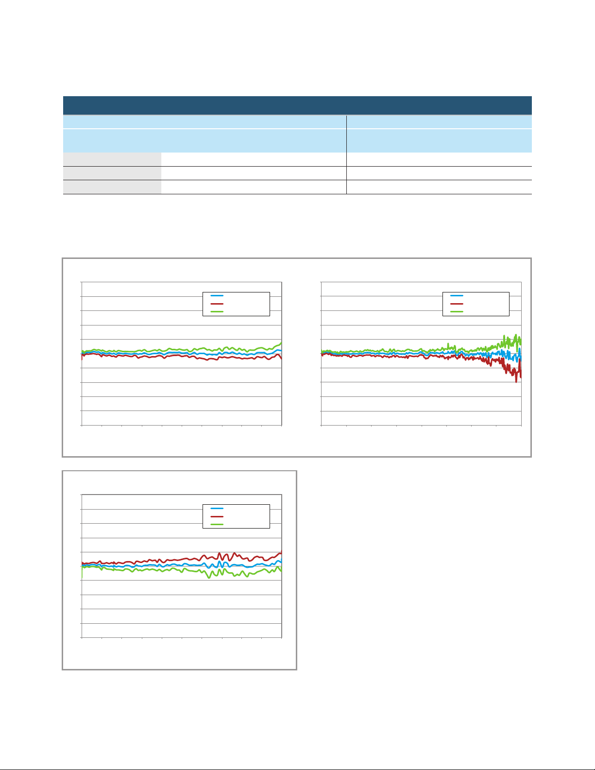
-1
-0.8
-0.6
-0.4
-0.2
0
0.2
0.4
0.6
0.8
1
02 468101214161820
mean
mean - std dev
mean + std dev
Frequency (GHz) vs. level accuracy ( dB)
Measured level accuracy at -110 dBm
Frequency (GHz) vs. level accuracy ( dB)
Measured level accuracy at -90 dBm
-1.00
-0.80
-0.60
-0.40
-0.20
0.00
0.20
0.40
0.60
0.80
1.00
0510 15 20 25 30 35 40
mean
mean - std dev
mean + std dev
Absolute level accuracy in CW mode
-1
-0.8
-0.6
-0.4
-0.2
0
0.2
0.4
0.6
0.8
1
02 468101214161820
mean
mean - std dev
mean + std dev
Frequency (GHz) vs. level accuracy ( dB)
Measured level accuracy at -120 dBm
1, 2
(ALC on) () = typical
With or without Option 1E1 With Option 1E1
9 kHz to 2 GHz
> 2 to 20 GHz
> 20 to 40 GHz
Max power to
+10 dBm
± 0.6 dB ± 0.6 dB ± 0.7 dB ± 0.7 dB ± 1.4 dB (± 0.3)
± 0.9 dB ± 0.7 dB ± 0.7 dB ± 0.7 dB ± 1.6 dB (± 0.3)
± 0.9 dB ± 0.8 dB ± 1.1 dB ± 1.1 dB ± 2.0 dB
< +10 to
–10 dBm
< –10 to
– 20dBm
< –20 to
–75 dBm
< –75 to
–90 dBm
< –90 to
–120 dBm
1. Level accuracy applies between 15 °C and 35 °C. Specifications do not apply above the maximum specified power. For temperatures outside this
range, absolute level accuracy degrades by 0.01 dB/degree C for frequencies ≤ 4.5 GHz and 0.02 dB/degree C for frequencies > 4.5 GHz.
2. For instruments with Type-N connectors (Option 1ED), specifications are degraded typically 0.2 dB above 18 GHz.
6
Page 7

SWR (measured CW mode)
Frequency Attenuator state
0 dB 5 dB and greater
≤ 2 GHz < 1.7:1 < 1.2:1
> 2 to 8 GHz < 1.4:1 < 1.4:1
> 8 to 13 GHz < 1.6:1 < 1.5:1
> 13 to 20 GHz < 1.8:1 < 1.7:1
> 20 to 40 GHz < 1.6:1 < 1.4:1
External detector leveling
Range –0.2 mV to –0.5 V (nom)
Bandwidth 10 kHz (typ)
Amplitude switching speed
SCPI mode ≤ 2 ms (typ)
Power search SCPI mode
List/step sweep mode ≤ 2 ms (typ)
1
2
3
< 12 ms (meas)
User flatness correction
Number of points 3201
Number of tables Dependent on available free memory in instrument; 10,000 maximum
Entry modes USB/LAN direct power meter control, LAN to GPIB and USB to GPIB, remote bus, and manual
USB/GPIB power meter control
Sweep modes
See Frequency Specifications section for more detail
1. Not intended for pulsed operation.
2. Time from receipt of SCPI command or trigger signal to amplitude settled within 0.2 dB. Specification does not apply when switching to or from frequencies < 5 MHz, or when ALC level is < 0 dBm, or when frequency crosses 0.002, 0.02, 0.1, 2.0, 3.2, 5.0, 6.4, 8, 10, 12.8, 16, 20, 25.6, or 32 GHz.
3. When ALC is off and power search mode is disabled amplitude switching is < 250 us (meas).
7
Page 8

Spectral Purity Specifications
-170
-160
-150
-140
-130
-120
-110
-100
-90
-80
-70
-60
-50
-40
-30
-20
1.E+00 1.E+01 1.E+02 1.E+03 1.E+04 1.E+05 1.E+06 1.E+07 1.E+08
L(f) [dBc/Hz] vs. f [Hz]
Standard SSB phase noise
40 GHz
20 GHz
10 GHz
3 GHz
1 GHz
250 MHz
100 MHz
-170
-160
-150
-140
-130
-120
-110
-100
-90
-80
-70
-60
-50
-40
-30
-20
1.E+00 1.E+01 1.E+02 1.E+03 1.E+04 1.E+05 1.E+06 1.E+07 1.E+08
M(f) [dBc/Hz] vs. f [Hz]
Measured AM noise
vs. power vs.S/N mode on/off at 10 GHz
10 GHz 0 dBm SNR OFF
10 GHz 0 dBm SNR ON
10 GHz +21 dBm SNR OFF
Standard absolute SSB phase noise (dBc/Hz) (CW) [at 20 kHz offset] 1 () = measured
5 to < 250 MHz –115 (–120)
250 MHz –129 (–134)
500 MHz –124 (–128)
1 GHz –118 (–122)
2 GHz –111 (–116)
3 GHz –105 (–110)
4 GHz –104 (–110)
6 GHz –99 (–104)
10 GHz –97 (–101)
20 GHz –90 (–95)
40 GHz –84 (–91)
Standard absolute SSB phase noise (dBc/Hz) (CW) [at 100 Hz offset] () = measured
100 MHz (–104)
250 MHz (–115)
500 MHz (–110)
1 GHz (–104)
2 GHz (–97)
3 GHz (–93)
4 GHz (–91)
6 GHz (–89)
10 GHz (–83)
20 GHz (–76)
40 GHz (–70)
1. From 0 to 55 °C, measured at +10 dBm.
8
Page 9

Broadband noise 1 () = measured
100 MHz (–143 dBc/Hz)
500 MHz (–155 dBc/Hz )
1 GHz (–163 dBc/Hz )
10 GHz (–150 dBc/Hz)
20 GHz (–143 dBc/Hz)
40 GHz (–135 dBc/Hz)
Residual FM (CW mode, rms) See frequency band table for N value
0.3 to 3 kHz bandwidth < N* 0.5 Hz (meas)
0.05 to 15 kHz bandwidth < N* 3 Hz (meas)
Residual AM (CW mode, +10 dBm, 0.3 kHz to 3 kHz bandwidth, rms)
< 2 GHz < 0.01% (meas)
Harmonics [CW mode] 2 () = typical
Range CW mode at +10 dBm CW mode at +20 dBm
9 kHz to 200 MHz < –48 dBc (–54) < –38 dBc (–43)
> 200 MHz to 2 GHz < –33 dBc (–40) < –25 dBc (–31)
> 2 to 20 GHz < –55 dBc (–65) < –50 dBc (–55)
1. CW mode at +10 dBm for offsets > 10 MHz. In high signal to noise ratio mode (optimize S/N).
2. Specifications apply from +15 to +35 °C and are nominal for harmonics beyond specified frequency range.
3. Or maximum specified output power, whichever is lower.
3
9
Page 10

Option 520 harmonics at +10 dBm (measured)
–30
Option 520 harmonics at +20 dBm (measured)
–30
–40
–50
–60
–70
2nd harmonic (dBc)
–80
–90
0 5000 10000 15000
Frequency (MHz)
Option 540 harmonics at +10 dBm (measured)
–30
–40
–50
–60
20000 25000
–40
–50
–60
–70
2nd harmonic (dBc)
–80
–90
0 5000 10000 15000
Frequency (MHz)
Option 540 harmonics at +20 dBm (measured)
–30
–40
–50
–60
20000 25000
–70
2nd harmonic (dBc)
–80
–90
0 5000 10000 15000
Frequency (MHz)
20000 25000
–70
2nd harmonic (dBc)
–80
–90
0 5000 10000 15000
Frequency (MHz)
20000 25000
10
Page 11

Nonharmonics (CW mode)
Range > 10 kHz offset
9 kHz to < 5 MHz –65
5 to < 250 MHz –75
250 to < 750 MHz –78
750 MHz to < 1.5 GHz –72
1.5 to < 3 GHz –66
3 to < 20 GHz –60
20 to 40 GHz –54
1, 2
Standard (dBc)
Subharmonics (CW mode)
9 kHz to 1.5 GHz None
> 1.5 to 3.2 GHz –75
> 3.2 to 5 GHz –67
> 5 to 10 GHz –67
> 10 to 20 GHz –56
> 20 to 40 GHz –53
1. CW mode at +10 dBm.
2. Power line related non-harmonics : 60 Hz to 300 Hz: < –50 dBc. Measured from 1 MHz to 40 GHz.
Jitter 1 (measured)
Carrier frequency SONET/SDH data rate rms jitter BW μUI rms Picoseconds
155 MHz 155 MB/s 100 Hz to 1.5 MHz 126 0.8
622 MHz 622 MB/s 1 kHz to 5 MHz 62 0.1
2.488 GHz 2488 MB/s 5 kHz to 20 MHz 251 0.1
9.953 GHz 10 kHz to 80 MHz 939 0.094
39.812 GHz 40 kHz to 320 MHz 3408 0.086
1. Calculated from phase noise performance in CW mode at +10 dBm. For other frequencies, data rates, or bandwidths, please consult your sales
representative.
11
Page 12

Analog Modulation Specifications
Frequency bands
Band # Frequency range N
1 9 kHz to < 5 MHz Digital synthesis
2 5 to < 250 MHz 1
3 250 to < 375 MHz 0.25
4 375 to < 750 MHz 0.5
5 750 MHz to < 1.5 GHz 1
6 1.5 to < 3 GHz 2
7 3 to < 6 GHz 4
8 6 to < 12 GHz 8
9 12 to < 24 GHz 16
10 24 to 40 GHz 32
Frequency modulation (Option UNT) (See N value above)
Max deviation N x 10 MHz (nom)
Resolution 0.025% of deviation or 1 Hz, whichever is greater (nom)
Deviation accuracy < ± 2% + 20 Hz 2 [1 kHz rate, deviation is N x 50 kHz]
Modulation frequency response
@ 100 KHz rate
Carrier frequency accuracy < ± 0.2% of set deviation + (N × 1 Hz)
Relative to CW after DC cal < ± 0.06% of set deviation + (N × 1 Hz) (typ)
Distortion < 0.4% [1 kHz rate, deviation is N x 50 kHz]
FM using external inputs 1 or 2 Sensitivity +1 V peak for indicated deviation (nom)
1 dB bandwidth DC/5 Hz to 3 MHz (nom)
3 dB bandwidth DC/1 Hz to 7 MHz (nom)
Input impedance 50 Ω/600 Ω/1 MΩ (nom)
Paths FM path 1 and FM path 2 are summed
1
3
4
internally for composite modulation
Phase modulation (Option UNT) (See N value above)
Maximum deviation Normal bandwidth N × 5 radians (nom)
High-bandwidth mode N × 0.5 radians (nom)
Frequency response Normal bandwidth (3 dB) DC to 1 MHz (nom)
High-bandwidth mode (3 dB) DC to 4 MHz (nom)
Resolution 0.1% of deviation
Deviation accuracy < +0.5% + 0.01 rad (typ) [1 kHz rate, normal BW mode]
Distortion < 0.2% (typ) [1 kHz rate, N x 1 radian deviation normal BW mode]
ΦM using external inputs 1 or 2 Sensitivity +1 V peak for indicated deviation (nom)
Input impedance 50 Ω or 600 Ω or 1 MΩ (nom)
Paths ΦM path 1 and ΦM path 2 are summed
internally for composite modulation
1. Digital synthesis band FM deviation is 5 MHz.
2. Specification applies from 15 to 35 °C.
3. Specification valid for temperature changes of less than ± 5 °C since last DC calibration.
4. Typical performance immediately after a DC calibration.
12
Page 13

Amplitude modulation (Option UNT)
1
Depth Linear mode Exponential mode
Settable depth
0 to 100% 0 to 50 dB
ALC ON with deep AM (default) or
2
ALC off
Depth resolution 0.1% (nom) 0.01 dB (nom)
AM depth accuracy
ALC on 3
[@ 1KHz rate, < 80% depth]
f < 5 MHz < 1.5% of setting +1%
± 2 dB @ 40 dB depth (typ)
(typ 0.5% of setting +1%)
5 MHz ≤ f ≤ 3.2 GHz < 4% of setting + 1% ± 2 dB @ 40 dB depth (typ)
> 3.2 to 40 GHz (typ 3% of setting +1%) ± 4 dB @ 40 dB depth (typ)
Total harmonic distortion (@ 1 KHz rate)
f < 5 MHz 30% depth < 0.25% (typ)
80% depth < 0.5% (typ)
5 MHz < f < 40 GHz 30% depth < 2%
80% depth < 3%
Frequency response (30% depth, 3 dB BW)
9 kHz to ≤ 3.2 GHz DC/10 Hz to 50 kHz
> 3.2 to 40 GHz DC/10 Hz to 100 kHz
5
5
AM inputs using External Inputs 1 and 2
Sensitivity +1 V peak for indicated depth (over-range can be 200% or 2.2 V peak)
Input impedance 50 Ω or 600 Ω or 1 MΩ, damage level: ± 5 V max
Paths AM Paths 1 and 2 are summed internally for composite modulation
4
4
4
Simultaneous and composite modulation
Simultaneous modulation All modulation types (FM, AM, φM and pulse modulation) may be simultaneously enabled except:
FM and phase modulation cannot be combined; two modulation types cannot be simultaneously
generated using the same modulation source. For example the Pulse, AM, and FM can run
concurrently and all will modulate the output RF. This is useful for simulating signal impairments,
FM chirp RADAR, or scan modulation.
Composite modulation AM, FM, and ΦM each consist of two modulation paths which are summed internally for
composite modulation. Modulation can be any combination of internal or external sources.
AM FM Phase Pulse
AM + + + +
FM + + – +
Phase + – + +
Pulse + + + –
+ = compatible, – = incompatible
1. AM specifications apply 6 dB below maximum specified power and down to –15 dBm for Option 520 or –20 dBm for Option 540 from 15 to 35 °C
with ALC on.
2. ALC off is used for narrow pulse modulation and/or high AM depths with envelope peaks below ALC operating range. Carrier power level will be
accurate after a power search is executed.
3. Deep AM with ALC on provides increased AM depths and improved distortion, together with closed-loop internal leveling. This mode requires a
repetitive AM waveform (frequency > 10 Hz) with peaks > –5 dBm (nom), excluding step-attenuator setting).
4. ± 2 dB @ 40 dB, and 50 dB < 31.8 GHz, and ± 4 dB @ 50 dB > 31.8 GHz (meas).
5. From 5 MHz to 50 MHz carrier roll off is < 5 dB at 50 kHz rate. From 50 MHz to 3.2 GHz rate is useable up to 100 kHz. Above 3.2 GHz rate is useable
to 1 MHz.
13
Page 14

External modulation inputs
(Option UNT required for FM, AM, and phase modulation inputs; Option UNW required for pulse modulation inputs)
EXT1 AM, FM, PM
EXT2 AM, FM, PM
PULSE Pulse (50 Ω only)
Input impedance 50 Ω, 1 MΩ, 600 Ω, DC and AC coupled
Standard internal analog modulation source
(Waveform generator for use with AM, FM, phase modulation, and LF out; requires Option UNT)
Waveform Sine, square, triangle, positive ramp, negative ramp
Rate range 0.1 Hz to 2 MHz (tunable to 3 MHz)
Resolution 0.1 Hz
Frequency accuracy Same as RF reference source (nom)
LF audio output 0 to 5 V peak into 50 Ω, –5 V to 5 V offset (nom)
Multifunction generator (Option 303)
The multifunction generator option (Option 303) consists of 7 waveform generators that can be set independently with up to 5
simultaneously using the composite modulation features in AM, FM/PM plus LF out
Waveform
Function generator 1 Sine, triangle, square, pos ramp, neg ramp, pulse
Function generator 2 Sine, triangle, square, pos ramp, neg ramp, pulse
Dual function generator Sine, triangle, square, pos ramp, neg ramp, pulse, phase offset and amplitude
ratio for Tone2 relative to Tone1
Swept function generator Sine, triangle, square, pos ramp, neg ramp
Trigger: free run, trigger key, bus, external, internal, timer trigger
Noise generator 1 Uniform, Gaussian
Noise generator 2 Uniform, Gaussian
DC Only for LF output
Frequency parameters
Sine wave 0.1 Hz to 10 MHz
Triangle, square, ramp, pulse 0.1 Hz to 1 MHz
Noise bandwidth 10 MHz
Resolution 0.1 Hz
Frequency accuracy Same as RF reference source (nom)
Narrow pulse modulation (Option UNW or UW2)
On/off ratio > 80 dB (typ)
Rise/fall times (Tr, Tf) < 10 ns; 7 ns (typ)
Minimum pulse width ALC on/off
Repetition frequency ALC on/off 10 Hz to 500 kHz / DC to 10 MHz
Level accuracy (relative to CW) ALC on/off
Width compression (RF width relative to video out) < 5ns (typ)
1. Pulse specifications apply to frequencies > 100 MHz. and power set to > –3 dBm. Operable down to 10 MHz.
2. Above 35 GHz vernier > 0 dBm.
3. For export control purposes option UW2 limits minimum pulse width above 31.8 GHz to ≥ 500 ns.
4. With power search on.
3
4
1
2
≥ 1us (500 ns typ) / ≥ 20 ns
± 0.7 dB (± 0.5 typ) / (< ± 0.75 dB typ)
14
Page 15

Video feed-through 1 < 3.2 / > 3.2GHz < 50 mV (typ) / < 3 mV (typ)
Sync
Output
Video
Output
RF Pulse
Output
T
d
T
m
T
w
T
rf
V
f
T
f
T
r
V
or
T
p
50%
50%
10%
90%
50%
Video delay (external input to video) 40 ns, nominal
RF delay (video to RF output) 45 ns, nominal
Pulse overshoot < 10% (typ)
Input level +1 V peak = RF On into 50 Ω (nom)
Td video delay (variable)
Tw video pulse width (variable)
Tp pulse period (variable)
Tm RF delay
Trf RF pulse width
Tf RF pulse fall time
Tr RF pulse rise time
Vor pulse overshoot
Vf video feedthrough
Internal pulse generator (included with Option UNW or UW2)
Modes Free-run, square, triggered, adjustable doublet, trigger doublet, gated, and
external pulse
Square wave rate 0.1 Hz to 10 MHz, 0.1 Hz resolution (nom)
Pulse period 30 ns to 42 s (nom)
Pulse width
Resolution 10 ns
Adjustable trigger delay (–pulse period +10 ns) to (pulse width –10 ns)
Settable delay Free run –3.99 to 3.97 µs
Resolution (delay, width, period) 10 ns, nominal
Pulse doublets 1st pulse delay (Relative to sync out) 0 to 42 s – pulse width – 10 ns
2
20 ns to pulse period –10 ns (nom)
Triggered 0 to 40 s
1st pulse width 20 ns to 42 s – delay – 10 ns
2nd pulse delay 0 to 42 s – (delay1 + width2) – 10 ns
2nd pulse width 20 ns to 42 s – (delay1 + delay2) – 10 ns
Pulse train generator Option 320 (requires Option UNW or UW2)
Number of pulse patterns 2047
On/off time range
1. Video feed through applies to power levels < +10 dBm.
2. For export control purposes option UW2 limits minimum pulse width above 31.8 GHz to ≥ 500 ns.
2
20 ns to 42 s
15
Page 16

General Characteristics
Remote programming
Interfaces GPIB IEEE-488.2, 1987 with listen and talk
LAN 1000BaseT LAN interface, LXI Class C compliant
USB Version 2.0
Control languages SCPI Version 1997.0
Compatibility languages Agilent Technologies: N5181A\61A, N5182A\62A, N5183A, E4438C, E4428C, E442xB,
E443xB, E8241A, E8244A, E8251A, E8254A, E8247C, E8257C/D, E8267C/D, 8648 series,
8656B, E8663B, 83711B/12B, 83731B/32B, 83751B/52B, 8340B/41B, 836xx series,
8664A, 8665A/B, 8644A, 8662A/63A
Aeroflex Incorporated: 3410 series
Rohde & Schwarz: SMR, SMF100A ,SMB100A, SMBV100A, SMU200A, SMJ100A,
SMATE200A, SMIQ, SML, SMV
Anritsu: MG369xA/B/C
Power requirements
100 or 120 VAC, 50 or 60 Hz, 400 Hz
220 or 240 VAC, 50 or 60 Hz
280 Watts maximum
Operating temperature range
0 to 55 °C
Storage temperature range
–40 to 70 °C
Operating and storage altitude
Up to 15,000 ft or 4,600 m
Environmental stress
Samples of this product have been type tested in accordance with the Agilent Environmental Test Manual and verified to be robust
against the environmental stresses of storage, transportation, and end-use; those stresses include but are not limited to temperature,
humidity, shock, vibration, altitude, and power line conditions. Test Methods are aligned with IEC 60068-2 and levels are similar to
MIL-PRF-28800F Class 3.
Safety
Complies with European Low Voltage Directive 2006/95/EC
• IEC/EN61010-1,3rdEdition
• Canada:CSAC22.2No.61010-1-12
• USA:UL61010-13rdEdition
EMC
Complies with European EMC Directive 2004/108/EC
• IEC/EN61326
• CISPRPub11Group1,classA
• AS/NZSCISPR11
• ICES/NMB-001
16
Page 17

Memory
Memory is shared by instrument states, user data files, sweep list files, and other files. Option 006 instrument security allows storage
of up to 8 GB. Depending on how the memory is utilized, a maximum of 1000 instrument states can be saved.
Security (Option 006)
Option 006 “Removable memory card & Instrument security” allows the following:
• Removable8GBsolidstatememory(SDcard)fromrearpane.
• Usercanforcealllestobestoredonlyonexternalmemorycardincludinginstrumentstates,userdatales,sweeplistles,
and other files
• Memorysanitizing,memorysanitizingonpoweron,anddisplayblanking
• DisableUSBports
Self-test
Internal diagnostic routines test most modules in a preset condition. For each module, if its node voltages are within acceptable limits,
the module “passes” the test.
Weight
N5173B-513/520: ≤ 14.5 kg (32 lb.) net, ≤ 29.5 kg (65 lb.) shipping
N5173B-532/540: ≤ 15.0 kg (33 lb.) net, ≤ 29.9 kg (66 lb.) shipping
Dimensions
88 mm H x 426 mm W x 489 mm L (length includes rear panel feet)
(3.5 in H x 16.8 in W x 19.2 in L)
Max length (L) including RF connector tip to end of rear panel feet is 508 mm (20 in)
Recommended calibration cycle
36 months
ISO compliant
This instrument is manufactured in an ISO-9001 registered facility in concurrence with Agilent Technologies’ commitment to quality.
17
Page 18

Inputs and Outputs
Front panel connectors (all connectors are BNC unless otherwise stated)
RF output Output impedance 50 Ω (nom)
Option 513/520 Precision APC-3.5 male, or Type- N with Option 1ED
Option 532/540 Precision 2.4 mm male; plus 2.4—2.4 mm and 2.4-2.9 mm female adapters
Maximum reverse power 0.5 W, 0 Vdc
USB 2.0 Used with a memory stick for transferring instrument states, licenses and other
files into or out of the instrument. Also used with U2000 Series USB average power
sensors.
Rear panel connectors
Rear panel inputs and outputs are 3.3 V CMOS, unless indicated otherwise. CMOS inputs will accept 5 V CMOS, 3 V CMOS, or TTL
voltage levels.
RF output (1EM) • Outputimpedance50Ω(nom)
• Option513/520:PrecisionAPC-3.5male,orType-Nwithoption1ED
• Option532/540:Precision2.4mmmale;plus2.4—2.4mmand2.4-2.9mmfemale
adapters
Sweep out Generates output voltage, 0 to +10 V when the signal generator is sweeping. This
output can also be programmed to indicate when the source is settled or output pulse
video and is TTL and CMOS compatible in this mode. Output impedance < 1 Ω, can
drive 2 kΩ. Damage levels are ± 15 V.
Ext1 External AM/FM/PM #1 input: Nominal input impedance is 50 Ω/600 Ω/1MΩ
nominal: Damage levels are ± 5 V.
Ext2 External AM/FM/PM #2 input: Nominal input impedance is 50 Ω/600 Ω/1MΩ
nominal: Damage levels are ± 5 V.
Pulse External pulse modulation input. This input is TTL and CMOS compatible. Low logic
levels are 0 V and high logic levels are +1 V. Nominal input impedance is 50 Ω. Input
damage levels are ≤ –0.3 V and ≥ +5.3 V.
Trigger 1 (in) Accepts TTL and CMOS level signals for triggering point-to-point in sweep mode.
Damage levels are ≤ –0.3 V and ≥ +5.3 V.
Trigger 2 (out) Default use is with sweep mode. The signal is high at start of dwell, or when waiting
for point trigger in manual sweep mode; low when dwell is over or point trigger is
received. This output can also be programmed to indicate when the source is settled,
pulse synchronization, or pulse video. Outputs a 2.5V into 50 Ω nominal. Input damage
levels are ≤ –0.3 V and ≥ +5.3 V.
Reference input Accepts a 10 MHz reference signal used to frequency lock the internal time base.
Option 1ER adds the capability to lock to a frequency from 1 MHz to 50 MHz. Nominal
input level –3.5 to +20 dBm, impedance 50 Ω, sine or square waveform.
10 MHz out Outputs the 10 MHz reference signal used by internal timebase. Level nominally
+5 dBm. Nominal output impedance 50 Ω. Input damage level is +16 dBm.
ALC in This female BNC connector is used for negative external detector leveling.
• Inputimpedance:100kΩ(nominal)
• Signallevels:–0.2mVto–0.5V
• Damagelevels:<–12Vand>1V
Z-Axisoutput This female BNC connector supplies a +5 V (nominal) level during retrace and band
switch intervals of a step or list sweep. During step or list sweep, this connector
supplies a –5 V (nominal) level when the RF frequency is at a marker frequency and
intensity marker mode is on. The load impedance should be ≥ 5 kΩ.
18
Page 19

USB Type-A There are two USB 2.0 Type-A connectors on the rear panel. Used with a memory stick
for transferring instrument states, licenses and other files into or out of the instrument;
also used with U2000 Series USB power sensors.
USB Type-B There is one USB 2.0 Type-B connectors on the rear panel. The USB connector
provides remote programming functions via SCPI.
LAN (1000 BaseT) The LAN connector provides the same SCPI remote programming functionality as the
GPIB connector. The LAN connector is also used to access the internal web server
and FTP server. The LAN supports DHCP, sockets SCPI, VXI-11 SCPI, connection
monitoring, dynamic hostname services, TCP keep alive. This interface is LXI class C
compliant. Trigger response time for the immediate LAN trigger is 0.5 ms (minimum),
4 ms (maximum), 2 ms (typ); delayed/alarm trigger is unknown. Trigger output
response time is 0.5 ms (minimum), 4 ms (maximum), 2 ms typical.
GPIB The GPIB connector provides remote programming functionality via SCPI.
19
Page 20

Related Literature
Agilent X-Series Signal Generators
MXG Microwave Signal Generator Data Sheet 5991-3131EN
Microwave Signal Generator Flyer 5991-3594EN
X-Series Signal Generator Brochure 5990-9957EN
myAgilent
www.agilent.com/find/myagilent
A personalized view into the information most relevant to you.
www.lxistandard.org
LAN eXtensions for Instruments puts the power of Ethernet and the
Web inside your test systems. Agilent is a founding member of the
LXI consortium.
Three-Year Warranty
www.agilent.com/find/ThreeYearWarranty
Agilent’s combination of product reliability and three-year warranty
coverage is another way we help you achieve your business goals:
increased confidence in uptime, reduced cost of ownership and
greater convenience.
www.agilent.com/quality
Agilent Electronic Measurement Group
DEKRA Certified ISO 9001:2008
Quality Management System
Agilent Channel Partners
www.agilent.com
www.agilent.com/find/N5173B
For more information on Agilent
Technologies’ products, applications or
services, please contact your local Agilent
office. The complete list is available at:
www.agilent.com/find/contactus
Americas
Canada (877) 894 4414
Brazil (11) 4197 3600
Mexico 01800 5064 800
United States (800) 829 4444
Asia Pacific
Australia 1 800 629 485
China 800 810 0189
Hong Kong 800 938 693
India 1 800 112 929
Japan 0120 (421) 345
Korea 080 769 0800
Malaysia 1 800 888 848
Singapore 1 800 375 8100
Taiwan 0800 047 866
Other AP Countries (65) 375 8100
Europe & Middle East
Belgium 32 (0) 2 404 93 40
Denmark 45 45 80 12 15
Finland 358 (0) 10 855 2100
France 0825 010 700*
*0.125 €/minute
Germany 49 (0) 7031 464 6333
Ireland 1890 924 204
Israel 972-3-9288-504/544
Italy 39 02 92 60 8484
Netherlands 31 (0) 20 547 2111
Spain 34 (91) 631 3300
Sweden 0200-88 22 55
United Kingdom 44 (0) 118 927 6201
For other unlisted countries:
www.agilent.com/find/contactus
(BP-09-27-13)
Product specifications and descriptions in
this document subject to change without
notice.
www.agilent.com/find/channelpartners
Get the best of both worlds: Agilent’s measurement expertise and
product breadth, combined with channel partner convenience.
© Agilent Technologies, Inc. 2013
Published in USA, November 13, 2013
5991-3132EN
 Loading...