

Page 1
The IFR 3410 series are portable, lightweight signal generators covering a wide range of carrier frequencies to 6 GHz. High quality analog and vector modulation capabilities make these signal generators
ideal for research, development and manufacturing applications.
Careful attention to the design of the modulators and the RF system
ensures that these signal generators exhibit low levels of adjacent
channel power, making them suitable for the most demanding
amplifier linearity and receiver selectivity measurements.
The use of Aeroflex fractional N synthesis techniques, combined
with fast level control and an electronic attenuator, ensures the 3410
series signal generators are both frequency and level agile for high
speed ATE testing.
A flexible but intuitive user interface based on a touch panel display
system ensures that the signal generator meets the needs of
unskilled as well as skilled operators. The instrument can be configured to the required mode of operation very simply, with numerical data being entered by the keyboard or via a rotary control. T he
display shows the primary parameters in a clear and unambiguous
format, minimizing the risk of operator error.
The 3410 series signal generators provide peak output power of up
to +16 dBm. With a level resolution of 0.01 dB, repeatable and accurate testing of wireless components can be performed.
Page 2
The electronic attenuator is ideal for high volume applications where
attenuator life is critical. A user defined RF level limit can be entered
to ensure that the signal generator cannot provide damaging signal
levels when testing less robust components. Careful attention to the
level control system guarantees that positive level transients cannot be
generated. The fast responding electronic reverse power protection
system helps ensure long life and high reliability when testing high
power systems.
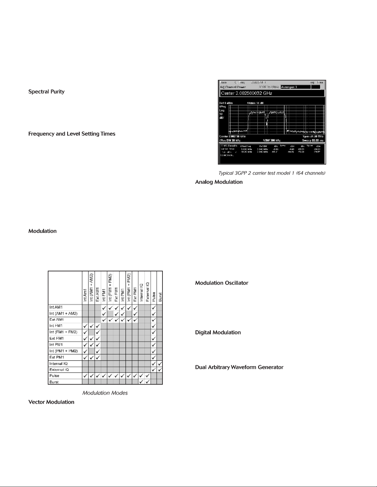
Receiver measurements require good spectral purity from a signal
generator. The 3410 series has excellent performance with typically
1.5 Hz residual FM at 1 GHz and a floor noise of typically better than
-148 dBc / Hz.
Fast frequency and RF level setting times are key parameters in
achieving minimum test execution times and therefore maximum
throughput, in production environments. The 3410 series with typical frequency setting times of 2 ms and level setting times of 2.5 ms
provide outstanding performance.
In addition to comprehensive sweep functions for carrier frequency,
RF level and modulation oscillator 3410 series provides an extremely
fast optional sweep mode for frequency and level settings through the
use of user stored lists. Option 010, List Mode has a setting time of
less than 500 µs and is ideal for frequency hopping and semi-conductor production applications.
Comprehensive modulation facilities are provided for supporting the
testing of analog or digital RF systems. A single key press turns the
modulation on and off, providing a fast method for signal to noise
checking.
be quickly optimized to reduce vector errors and ensure low carrier
leak at all operating frequencies.
The linearity of the modulator and the RF output system is reflected
in the excellent adjacent channel power when generating multi-carrier non-constant envelope signals such as cellular CDMA and
TETRA.
With typical AM bandwidth to 30 MHz and typical FM bandwidth to
20 MHz, the 3410 series signal generators are ideal tools for testing
broadcast systems. The wide bandwidths allow video signals to modulate the carrier with minimal distortion.
The wideband FM facilities allow the generation of fast-swept signals, while the use of a patented DC FM system ensures that carrier
frequency errors when the FM is DC coupled are minimal.
The specifications for AM are maintained to high carrier frequencies
to support the use in modern EMC testing applications. The signal
generator maintains excellent phase noise performance even when
generating wideband modulated signals.
The built-in IQ modulator provides state-of-the-art vector modulated signals with excellent level linearity, low vector error and low noise.
With a typical vector bandwidth up to 55 MHz, the modulator is able
to support wideband as well as narrow-band wireless standards.
Internal calibration systems ensure the modulator performance can
An internal modulation oscillator is provided which can be used to
generate two tones in the frequency range 0.1 Hz to 50 kHz (16 MHz
with Option 005 ARB Waveform Generator). In addition to sine
waves, the modulation oscillator can provide square waves, triangular
and sawtooth waveforms for narrow band sweeping.
The user has a choice of either a Dual Arbitrary Waveform Generator
or a Real Time Baseband Generator for producing digitally modulated output signals.
Fitted internally, the optional Dual Channel Arbitrary Waveform
Generator allows the user to select from a library of pre-stored IQ
modulator drive waveforms to provide accurately modulated carriers
simulating the characteristics of digitally modulated communication
systems. Burst modulation and alternate level rf attenuation facilities
are provided for TDMA signal simulation. Marker output signals can
be placed within the waveform to simplify triggering and synchronization with external test equipment. Using a patented technique,
the dual channel ARB is able to take waveform files typically four
times oversampled and run them through a real time interpolation
Page 3

system to raise the sampling rate of the file. This ensures the generation of low adjacent channel power and low spectral noise density.
The dual channel ARB is suited for the generation of both narrow
band and wideband signals, including WCDMA signals, without the
use of switched reconstruction filters. Combining a large ARB memory with the smaller file size required to define a waveform allows the
ARB to store up to 180 waveforms. Alternatively the whole of the
memory can be devoted to a single file. One such file would store over
1.5 seconds of a 3GPP WCDMA waveform signal. The use of interpolation techniques ensures that when narrow band systems are simulated the waveform generator can still operate at a high sample rate
without requiring excessively large amounts of data to be loaded or
restricting the repetition time. The library waveforms are structured
in a directory form to ease their selection and the optimization of the
user's generator. The modulation waveforms can be simply changed
by selection from a file list with the changeover between waveforms
occurring in a few milliseconds rather than the many seconds
required in more traditional waveform generators. The file name can
be determined by the user to convey a useful description of the contents of the file.
is a Windows based software utility that enables a user to
set up a modulation scheme and then create an ARB file using modulation templates. The resulting file may be saved on a PC or downloaded into the ARB. User-defined configurations can also be saved.
Consequently, it is possible to load previously saved setups to regenerate the ARB files quickly and easily. The capabilities of
include:-
Generic Modulation Types
PSK, FSK, MSK, QAM modulation types
Nyquist, Root Nyquist and Gaussian filters
PRBS, fixed pattern and user defined data sources
IQ errors - residual carrier, IQ imbalance, quadrature offset
Multi-carrier
Also included are 2G, 2.5G and 3G cellular TDMA and CDMA digital standards along with WLAN and other cordless phone standards.
In addition, includes a utility that allows user-defined
waveforms, created using software simulation tools such as
MATLAB, to be converted and packaged into a form that can be
downloaded into the 3410 Series ARB.
Fitted internally, the optional Real Time Baseband, RTBB, generates
baseband signals (I and Q) that modulate an RF source in real time
to produce generic FSK, PSK and QAM signals at rates up to
2 Msymbols/sec. The RTBB generates or inputs a set of modulation
symbols, modulates them with the chosen scheme, filters them using
an appropriate channel filter, and then converts the digital stream to
analogue I and Q for the I/Q vector modulator. T he source of the
symbol data is very flexible. The symbol data can originate from a
variety of internal or external sources. Internal data source choices
include a PRBS generator, an internal pattern generator or internal
memory storage of user downloaded symbols. External real-time
symbol data can be input in serial or parallel format via an industry
standard Low Voltage Differential Signalling (LVDS) interface.
Digitized I/Q data, available from sources such as basestation simulators, can be input via the LVDS interface as an alternative to external parallel or serial symbol data. Streaming digitized I/Q data samples are available as an output via the LVDS interface from internally
generated symbols for testing D/A convertors.
Synchronized clock, RF Burst, RF Burst Attenuation control and
marker output signal facilities are available for both internal and
external data generation.
An important feature necessary to support GSM signal generation is
the ability to frequency hop between channels. The RTBB option
provides frequency hopping by re-mixing the I and Q data at baseband. The resultant I and Q vectors then modulate the core synthesizer frequency thus producing a new RF frequency at the output of
the signal generator. This method ensures that synchronization is
maintained between the IQ data and the hop trigger. In addition,
because the main synthesizer hardware remains unchanged, frequency stabilization is nearly instantaneous.
The 3410 series is supplied with a free copy of
, a software
package to aid the creation and download of files to the ARB and
RTBB options.
is continually updated to include new modulation capabilities and facilities. The latest version is available for download at
www.aeroflex.com.
Options to have an instrument's ARB pre-loaded with a suite of example waveform files are available. A selection of waveforms from each
of the standards, or just waveforms relevant to the user's applications,
can be chosen. Although only available at the time of order, all the
waveforms are available within IQCreator should any of the files be
deleted then required in the future.
Single ended baseband I/Q outputs are available as standard.
Differential I/Q outputs, combined with comprehensive voltage bias
and offset facilities, are optionally available to simplify component and
module testing.
An optional pulse modulator allows the generation of fast rise time RF
signals with on/off ratios that meet the most demanding radar and
ECM/ECCM test applications.
The 3410 series include both fast GPIB and Ethernet remote control
interfaces for flexibility in production environments. RS-232 control
is also provided for use in legacy ATE systems.
The protocol and syntax of the GPIB commands have been designed
in accordance with IEEE 488.2 to simplify program generation. Plug
and play drivers are available that include a virtual front panel for
remote instrument supervision and debug.
The 3410 series includes a high stability OCXO as standard. The
inclusion of a main input power standby mode maintains the oscillator at working temperature while the rest of the instrument is powered down. Time to full specification working is thereby minimized
for equipment facilities held on standby.
Page 4
The 2U rack height ensures the 3410 series occupies minimal space
in a manufacturing rack or on the engineer's bench, allowing the provision of more compact test systems. The full rack width ensures
easy stacking of instruments while the light weight allows for easy
carrying in the laboratory or the field.
Range
250 kHz - 2 GHz (3412)
250 kHz - 3 GHz (3413)
250 kHz - 4 GHz (3414)
250 kHz - 6 GHz (3416)
Resolution
1 Hz, accuracy as frequency standard
The carrier output phase can be advanced or retarded in increments of
0.036°.
FREQUENCY SETTING TIME (NON-LIST MODE)
After receipt of the GPIB interface deliminator (terminator), 23°C ± 5°C
Phase Noise Mode Optimized > 10 kHz
< 5.5 ms, typically 4 ms, 375 MHz, to be within 200 Hz
Phase Noise Mode Optimized < 10 kHz
< 3 ms, typically 2.5 ms, 375 MHz, to be within 200 Hz
< 2.5 ms, typically 2 ms, >375 MHz, to be within 0.1 ppm
FREQUENCY SETTING TIME (OPTION 010 LIST MODE)
After external trigger in List Mode, 23°C ± 5°C
Phase Noise Mode Optimized > 10 kHz
< 4 ms, typically 3 ms, 375 MHz, to be within 200 Hz
Phase Noise Mode Optimized < 10 kHz
<600
s, typically 500 s,375 MHz, to be within < 200 Hz
<500
s, typically 450 s, > 375 MHz, to be within 0.1 ppm
> 375 MHz, to be within 0.1 ppm
> 375 MHz, to be within 0.1 ppm
When IQmodulation is selected maximum output is reduced by 6 dB
below 100 MHz.
Resolution
0.01 dB
RF Level Units
Units can be set to µV, mV, V EMF or PD; dB relative 1 µV, 1 mV, 1 V
EMF or PD; or dBm. Conversion between dB and linear units may be
achieved by pressing the appropriate units key (dB or V, mV or µV).
RF Output Accuracy (@ 23°C ± 5°C)
Electronic Attenuator
RFMode -127 to -30 dBm > -30 dBm
Auto
Mechanical Attenuator
RFMode -127 to -28 dBm > -28 dBm
Auto
No Attenuator
RFMode > 0 dBm
Auto
Level Accuracy With IQ Modulation
For constant envelope modulation systems: typical standard level error
± 0.15 dB
For non-constant envelope modulation systems: typical standard level
error ± 0.25 dB
Temperature Stability
± 0.01 dB/°C, 3 GHz
± 0.02 dB/°C, 4 GHz, ± 0.02 dB/°C typical, 6 GHz
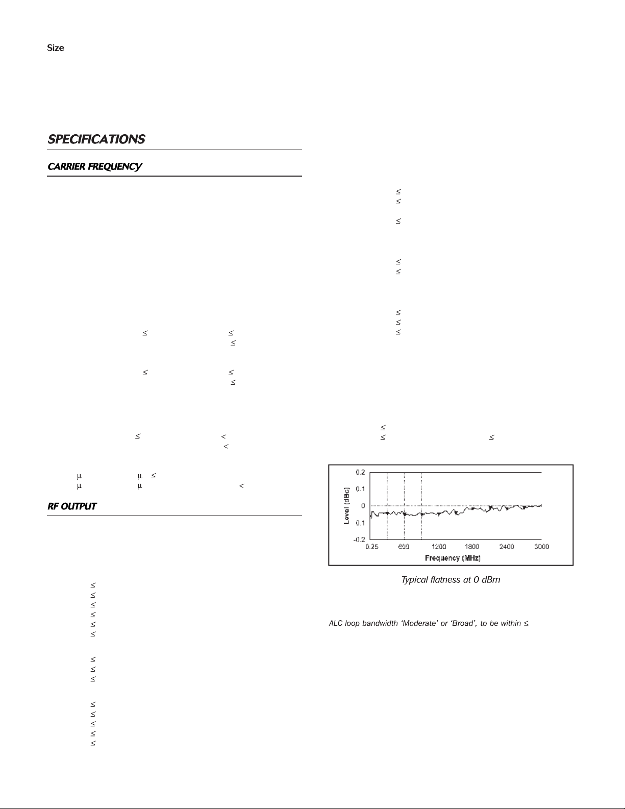
RF Flatness
2 GHz ± 0.75 dB ± 0.50 dB
3 GHz ± 1.00 dB ± 0.75 dB
-110 to -30 dBm > -30 dBm
6 GHz ± 1.25 dB ± 1.00 dB
2 GHz ± 0.75 dB ± 0.50 dB
3 GHz ± 1.00 dB ± 0.75 dB
2 GHz ± 0.50 dB
3 GHz ± 0.75 dB
6 GHz ± 1.00 dB
The RF output is controlled by an ALC system in normal operation.
When IQ modulation is enabled alternative control modes are available
to optimize the performance of the signal generator.
Range
Electronic Attenuator
10 MHz -140 to + 13 dBm
2 GHz -140 to + 16 dBm
3 GHz -140 to + 16 dBm
3.75 GHz -140 to + 13 dBm
4 GHz -140 to + 10 dBm
6 GHz -140 to + 8 dBm
Mechanical Attenuator
10 MHz -140 to + 16 dBm
2 GHz -140 to + 19 dBm
3 GHz -140 to + 16 dBm
No Attenuator
10 MHz 0 to + 21 dBm
3 GHz 0 to + 22 dBm
3.75 GHz 0 to + 20 dBm
4 GHz 0 to + 17 dBm
6 GHz 0 to + 18 dBm
When AM is selected the maximum RF output is linearly reduced by up
to 6 dB depending on the requested AM depth.
LEVEL SETTING TIME
Electronic attenuator, Option 003 is assumed in all cases.
0.3 dB
Level Setting Time (Non-List Mode)
After receipt of the GPIB interface deliminator (terminator), 23°C ± 5°C
< 4.5 ms, typically 2.5 ms
Level Setting Time (Option 010 List Mode)
After external trigger in List Mode, 23°C ± 5°C
< 3 ms, typically 1.5 ms
Page 5

Output VSWR
Electronic Attenuator
For output levels < 0 dBm Frequency Output VSWR
2 GHz < 1.25:1
3 GHz < 1.40:1
4 GHz < 1.50:1
6 GHz < 1.60:1
For output levels > 0 dBm VSWR is < 1.5:1 4 GHz, < 1.8:1 6 GHz
Mechanical Attenuator
For output levels < 0 dBm Frequency Output VSWR
3 GHz 1.33:1
For output levels > 0 dBm VSWR is < 1.5:1, 3 GHz
No Attenuator
Frequency Output VSWR
4 GHz < 1.5:1
6 GHz < 1.8:1
Attenuator Repeatability
Mechanical attenuator typically 0.1 dB
Output Connector
Front panel 50 type N female to MIL-PRF-39012 class 2
Output Protection
Protects the instrument from externally applied RF power
(from a 50 source) of 50 W up to 3 GHz and 25 W up to 4 GHz
The RPP trip may be reset from the front panel or via the remote interface. For safety, the protection is also provided when the instrument is
switched off.
3416 damage level 0.5 W (+ 27 dBm) from a max 5:1 VSWR, all frequencies
All parameters stated at RF level + 7 dBm in Noise and ACP RF
modes
Harmonics
< -30 dBc, typically < -40 dBc
Sub- and Non-Harmonics
For offsets > 10 kHz
< -70 dBc for carrier frequencies 3 GHz
< -60 dBc for carrier frequencies 6 GHz
Residual FM (FM on CW)
< 2.5 Hz RMS (typically 1.5 Hz) at 1 GHz in a 300 Hz to 3.4 kHz
unweighted bandwidth
SSB Phase Noise
For 20 kHz offset, Noise Optimized mode
CW/IQ
375 MHz < -115 dBc/Hz
500 MHz < -124 dBc/Hz
1 GHz < -118 dBc/Hz
2 GHz < -112 dBc/Hz
3 GHz < -108 dBc/Hz
4 GHz < -106 dBc/Hz
6 GHz < -102 dBc/Hz
Page 6

SSB AM Noise
SSB AM noise at 20 kHz offset (Typical values) measured at levels
> 0 dBm
Frequency MHz CW/IQ (dBc/Hz)
3 GHz -130
6 GHz -125
FREQUENCY MODULATION
Peak Deviation
Frequency Maximum Peak Deviation
250 kHz to 375 MHz 7.5 MHz
375 MHz to 750 MHz 3.75 MHz
750 MHz to 1.5 GHz 7.5 MHz
1.5 GHz to 3 GHz 15 MHz
3 GHz to 6 GHz 30 MHz
Displayed resolution is 4 digits or 1 Hz.
FM Accuracy
At 1 kHz rate
± 3% of set deviation excluding residual FM
FM Bandwidth
0.5 dB DC to 200 kHz (DC coupled, 100 k )
10 Hz to 200 kHz (AC coupled, 100 k )
3 dB Typically 20 MHz (DC or AC coupled, 50 )
RF Leakage
< 0.5 µV PD at the carrier frequency into a single turn 25 mm loop
25 mm or more from the case of the signal generator, for carrier frequencies <3 GHz
Wideband Noise
Applicable for all carrier levels at offsets > 5 MHz and < 50 MHz
excluding thermal noise (23°C ± 5°C)
RF Mode 375 MHz 3 GHz 6 GHz
(dBc/Hz) (dBc/Hz) (dBc/Hz)
Power < -138 < -142 (-148 typ) < -136
Noise < -138 < -142 (-148 typ) < -136
ACP < -135 < -140 < -134
FM, AM and M can be applied to the carrier using internal or external modulation sources. The internal modulation source is capable of
generating two simultaneous signals into any one of the modulation
channels. The internal and external modulation sources can be simultaneously enabled in order to produce combined amplitude and frequency (or phase) modulation.
Internal and external IQ modulation can be applied. In this mode, FM,
AM and M are not permitted.
Optional Pulse modulation can be used in combination with FM, AM,
M and IQ from an external pulse source.
Carrier Frequency Offset
For DC coupled FM ± (1 Hz + 0.1% of set deviation) after performing
a DCFM null operation
Total Harmonic Distortion
At 1 kHz rate
< 0.15% for deviations up to 2% of maximum allowed deviation
< 0.6% for deviations up to 20% of maximum allowed deviation
< 1.5% at maximum deviation
PHASE MODULATION
Phase Deviation
0 to 10 radians
Displayed resolution is 4 digits or 0.01 radians.
Accuracy
At 1 kHz rate
± 4% of set deviation excluding residual phase modulation
Bandwidth
0.5 dB 100 Hz to 10 kHz (AC coupled, 100 k )
Total Harmonic Distortion
At 1 kHz rate
< 0.5% at 10 radians deviation
Typically < 0.1% at 1 radian deviation
AMPLITUDE MODULATION
Specifications apply for carrier frequencies from 2 MHz up to 2 GHz,
Maximum specified output power is reduced by 2 dB,
Modulation Depth
0 to 99.9%, Displayed resolution is 3 digits or 0.1%
Page 7

Accuracy
At 1 kHz rate
± 4% of set depth ± 1% excluding residual AM
AM Bandwidth
1 dB DC to 200 kHz (DC coupled, 100 k )
10 Hz to 200 kHz (AC coupled, 100 k )
3 dB Typically 30 MHz (DC or AC coupled, 50 )
Total Harmonic Distortion
For 1 kHz modulation rate
< 1% for depths
< 2% for depths
30%
80%
FM on AM
Typically < 20 Hz for 30% AM depth at a modulation rate of 1 kHz and
carrier frequency of 500 MHz
M on AM
Typically < 0.02 radian for 30% AM depth at a modulation rate of
1 kHz and carrier frequency of 500 MHz
IQ MODULATION
Performance applicable in ACP and Noise modes only
IQ Inputs
BNC connector inputs, selectable 50 /100 k input impedance
Full scale input (I2+Q2)
0.5
occurs for 0.5 V rms (The level requested is
obtained by applying 0.5 VDC to either the I or Q input)
3 dB:
RF Mode 2.8 GHz 6 GHz
Noise > 42 MHz, 50 MHz typ > 35 MHz, 45 MHz typ
ACP > 48 MHz, 55 MHz typ > 40 MHz, 50 MHz typ
DC Vector Accuracy
Relative to Full Scale (0.5 V RMS)
Static Error Vector Magnitude (EVM) < 1% RMS at full scale
Magnitude error < 0.5% RMS at full scale
Phase error < 0.5° RMS at full scale
Residual Carrier Magnitude:
For 0 V input voltage, relative to full scale
RF Mode
Noise < -45 dBc, typically < -55 dBc
ACP < -40 dBc, typically < -50 dBc
Valid for 12 hours after executing an IQ self-calibration and within
± 5°C of the calibration temperature. The instrument displays a warning if the time or temperature limits are exceeded.
Static EVM and phase error measured with residual carrier magnitude
removed.
IQ Image Suppression
At 10 kHz modulation frequency
Typically < -50 dBc @ 10 kHz
Linearity (See linearity chart over page)
Adjacent Channel Power (ACP), in ACP mode for continuous and discontinuous signals at RF output levels 0 dBm, over the temperature
range 23°C ± 5°C
A digital control bit is used to generate an analog ramp (up or down)
of the RF output. The Burst Gate control signal can either be generated internally as part of the optional internal base-band source, or provided externally by the user on the rear panel connector. When internally generated, the Burst Gate control signal appears on the rear
panel auxiliary connector that then serves as an output.
On/Off Ratio
For the temperature range 23°C ± 5°C
> 90 dB for carriers 3 GHz
> 80 dB for carriers 4 GHz
> 65 dB for carriers 6 GHz
Ramp Profile
Rise and fall time after the L-H and H-L transitions of the burst control
bit respectively can be defined by the user from 10 µs to 999 µs in
0.1 µs steps.
Burst Gate control input is a TTL level (HCT), 50 impedance BNC
input on the rear panel.
RF ramp can be adjusted in time by ± 50 µs in increments of
0.1 µs with respect to the trigger event.
Modulation Bandwidth Relative to DC
At 23°C ± 5°C:
± 0.5 dB for frequencies DC up to 5 MHz
1 dB for frequencies DC up to 10 MHz
A digital attenuation control bit (in conjunction with the ramp control
bit) is used to decrease the RF level from the set level to an alternative
level during burst modulation. The Burst Attenuation Trigger signal can
be provided internally as part of the optional dual arbitrary waveform
generator (ARB), or externally on a rear panel connector. When internally generated, the Burst Attenuation Trigger control signal appears on
the rear panel auxiliary connector that then serves as an output.
Attenuation range available is 0 to 70 dB.
Burst Attenuation Trigger control is a TTL level (HCT), 50
impedance
Page 8

LINEARITY CHART
TETRA GSM 900 / 1800 / 1900 802.11a** IS-95 (CDMAone)
GSM EDGE (Enhanced Data Wireless LAN
rate for GSM Evolution) (Spectral Mask)
Frequency
Range(s)
ACLR
130 MHz - 1 GHz 850 MHz - 1 GHz 5.15 - 5.825 GHz 824 - 894 MHz
1700 - 1900 MHz 1850 - 2000 MHz
< -70 dBc @ 25 kHz offset < -35 dBc @ 200 kHz offset <-25 dBr @ 11 MHz offset < -65 dBc @ 885 kHz offset
(Continuous & < -80 dBc* @ 50 kHz offset < -70 dBc @ 400 kHz offset < -45 dBr @ 20 MHz offset < -75 dBc @ 1.25 MHz offset
Discontinuous)
< -80 dBc* @ 75 kHz offset < -80 dBc @ 600 kHz offset < -60 dBr* @ 30 MHz offset < -80 dBc @ 1.98 MHz offset
3GPP/WCDMA NADC (IS - 54, IS - 136) JDC/PDC PHP/PHS
Frequency
Range(s)
1855 - 2200 MHz 824 - 894 MHz 810 - 826 MHz 1895 - 1918 MHz
1850 - 2000 MHz 940 - 956 MHz
1429 - 1513 MHz
ACLR
< -70 dBc @ 5 MHz offset < -40 dBc @ 30 kHz offset < -65 dBc @ 50 kHz offset < -75 dBc @ 600 kHz offset
(Continuous & < -72 dBc* @ 5 MHz offset <-78 dBc* @ 60 kHz offset < -80 dBc* @ 100 kHz offset < -80 dBc @ 900 kHz offset
Discontinuous)
* denotes typical value ** At RFo/p level -4 dBm
< -80 dBc* @ 90 kHz offset
signal available on the rear panel Auxiliary connector.
RF burst attenuation requires Electronic Attenuator Opt 003.
A high performance Dual Arbitrary (ARB) Waveform Generator that provides IQ signals for the IQ modulator
The ARB enables files to be downloaded with sample rates from
17 kHz to 66 MHz. The ARB uses an interpolation system to increase
The internal modulation source is capable of generating up to two
simultaneous signals into any one of the modulation systems.
the digital to analog converter sample rate and avoid the use of reconstruction filters.
Frequency Range
0.1 Hz to 50 kHz (16 MHz with Option 005) with 0.1 Hz or 5 digits of
resolution
Accuracy
As frequency standard
Distortion
< 0.1 % for a sine wave at 1 kHz
In addition to a sine wave the following waveforms can be generated:
Triangle 0.1 Hz to 10 kHz (2 MHz with Option 005)
Ramp 0.1 Hz to 10 kHz (2 MHz with Option 005)
Square 0.1 Hz to 5 kHz (1 MHz with Option 005)
(Note: modulation frequency can be set to 50 kHz irrespective of
waveform type)
Level
Modulation source signals are available on the rear panel I/AM OUT
and Q/FM OUT at nominal level of 1 V peak EMF from 50
source
impedance.
ARB CHARACTERISTICS
Flash Memory Size
23,592,960 sample pairs
Maximum Number of Files
180
Sample Format
External inputs are available with a selectable input impedance of
50
or 100 k (default setting), AC or DC coupled.
Apply 1 V RMS (default) or 1 V peak for the set modulation.
A HI/LO indicator when the applied signal is greater than ± 6% from
nominal
External AM is input to EXT I/EXTAM front panel BNC connector.
External FM is input to EXT Q/EXT FM front panel BNC connector.
32 bits of data - 14 bits I, 14 bits Q, 3 associated marker bits
Sample Rate Tuning
± 20 ppm, 0.1 ppm step resolution
D-A Converter Resolution
14 bits
D-A Sample Rate
44 to 66 Msamples/s
Page 9

Interpolation Factor
Automatically selected
Reconstruction Filter Stop Band Attenuation
> 70 dB
ARB Spectral Purity
Spurious free dynamic range > 70 dB, typically > 80 dB
20 kHz offset phase noise < -120 dBc/Hz
Floor noise < -140 dBc/Hz
ation, formatting and downloading of ARB waveform files to the 3410
series.
A waveform library is provided on a CD containing a selection of files
for testing 2G, 2.5G and 3G systems. Files can be downloaded from
www.aeroflex.com.
Marker Control Bits
Up to 3 marker bits (1-3) can be attached to each sample of IQ data.
These can be used to indicate significant points in the waveform and
are available as HCCMOS outputs via the rear panel Aux IN/OUT connector. Marker bit 1 can be used as RF Burst Control signal. Marker
bit 2 can be used as Burst Attenuation Trigger signal to decrease
(attenuate) the RF level from its nominal value.
Control Mode
Continuous, single or triggered operation of the ARB
An external TTL trigger input signal is available on the AUX IN/OUT rear
panel connector.
IQ Outputs (Not applicable with Option 009 fitted)
The IQ signals produced by the ARB are available on the rear panel
I/AM OUT and Q/FM OUT BNC connectors. Output level is 0.5 V RMS
EMF (vector sum) from a source impedance of 50 .
Allows the creation of digitally modulated signals using generic modulation formats. An internal data source provides PRBSor fixed patterns.
External real-time data in the form of symbol data, or digital IQ data
may be applied via an LVDS interface.
Generic Modulation Formats
PSK BPSK, QPSK, 8PSK, 16PSK
8PSK EDGE (8PSK with 3 /8 rotation)
/2 DBPSK, /4 DQPSK, /8 D8PSK
DBPSK, DQPSK, D8PSK
OQPSK (time offset)
MSK GMSK
FSK/GFSK 2 and 4 level symmetric
QAM 16, 32, 64, 128, 256 levels
For data bit to symbol mapping information refer to Technical Note
"IFR 3410 Option 8 RTBB Ancillary Information"
SYMBOL RATE
Range
5 kHz to 2 MHz. Resolution 1 Hz
BASEBAND CHANNEL FILTERS
Filter Types
Nyquist a = 0.1 to 0.8, resolution 0.01
Root Nyquist a = 0.1 to 0.8, resolution 0.01
Gaussian Bt 0.1 to 1.0, resolution 0.1
EDGE "Linearized Gaussian" as defined in GSM 05.04
DATA SOURCE
Formats
Internal Data PRBS - PN9, PN11, PN15, PN16, PN20, PN21, PN23.
Fixed Pattern consisting of -
User-defined symbol file stored in non-volatile memory
(Max size 256 kB)
External Serial Data
A single bit stream representing symbol information can be applied.
The bit to symbol conversion is determined from the selected modulation type.
External Parallel Data
Symbol information consisting of 1 to 8 data bits can be applied.
External parallel and serial data is input via the LVDS connector on the
rear panel.
DATA ENCODING
None, Differential, GSM Differential, Inverted
TIMING/SYNCHRONIZATION
All clock and synchronization signals are provided internally by Option 8
RTBB and made available to the user on the rear panel LVDS connector. An external clock may be phase aligned to the internal clock via a
"sync" operation.
External Serial Data Clock
Eight times the symbol rate, for all modulation types.
External Parallel Data Clock
Nominal symbol rate
FREQUENCY HOPPING
Frequency Hop List
Up to 32 frequency values. The frequency values entered represent
offset values from the current RF frequency.
Frequency Offset Values
Offset values range ± 10 MHz
MODES
Linear
On receipt of a hop trigger, the next frequency in the list is indexed.
Random
On receipt of a hop trigger, an internal PRBS generator indexes
through the frequency list. PN length and polynomial initial seed value
are user selectable. PN values selectable from - 9, 11, 15, 16, 20,
21, and 23.
External
On receipt of a hop trigger, the 5-bit hop address lines applied to the
LVDS connector are used to index the frequency list.
Hop Rate
Max hop rate (hops/sec) is half symbol rate. Hopping is synchronized
to symbol transition.
DIGITAL IQ DATA
Digital IQ data is available via the LVDS connector on the rear panel.
EXTERNAL IQ DATA IN
External 16-bit IQ data can be applied to an LVDS interface. The data
can then be filtered or not, depending on the application, by the baseband board and fed to the DACs. All clock and sync signals are located
Page 10

on the LVDS connector. These can be used to synchronize to an externally applied clock.
INTERNAL IQ DATA OUT
16-bit IQ data is available on the LVDS interface when the modulation
is generated internally. Outputs can be disabled.
TONES
A tone (CW) only mode is available. Up to 2 tones may be selected.
Each tone may be independently enabled and disabled.
Frequency Range carrier frequency ± 10 MHz
Relative Level 60 dB
Logarithmic: 0.01% to 50%, 0.01% step
Level Sweep
0.01 dB minimum step
Modulation Oscillator
0.1 Hz minimum frequency step
LIST MODE
Up to 500 frequencies and levels can be entered in the list. Start
address, stop address and dwell time can be controlled. Dwell time
can be set from 500 µs to 10 s. Requires Option 003 Electronic
Attenuator
When differential I/Q outputs are enabled signal generator RF carrier
output is CW
Output Impedance
Can be used with single ended 50 loads or differential 100
Delivered bias voltages are halved with single ended loads.
I/Q Bias Voltages
Independent I and Q channel bias voltages settable within the range of
± 3 V
Bias Voltage
Resolution 1.0 mV nominal
Accuracy ±2% ± 4 mV max, ± 1% ± 2 mV typical
Offset See Bias Voltage above.
Differential Offset Voltage
Range ± 300 mV
Resolution 100 µV nominal
Accuracy ± 2% ±3.3 mV max, ± 1% ± 0.7 mV typical
Level Mode
Variable IQ signal level over 45 dB range
Differential Signal Balance
typ 0.15 dB @10 MHz
I/Q Channel Balance
± 0.2 dB @1 MHz
I/Q Level Imbalance Adjust
± 4 dB nominal continuously variable
I/Q Signal Amplitude
22.4 mV to 4 V pk-pk per channel
I/Q Signal Amplitude Accuracy
< 2% at 20 kHz, typ 1.5%, excludes termination errors
Baseband Purity (2 V p-p set voltage at 1 MHz)
2nd Harm -70 dBc
3rd Harm -65 dBc
IMD -70 dBc (100 kHz tone spacing, at 1 MHz)
Provides a digital sweep of RF frequency, RF level and Analog
Modulation Sources in discrete steps
Start, stop, step size, number and step time can be controlled. Step
time may be set from 2.5 ms to 10 s with 0.1 ms resolution. (20 ms
for mechanical attenuator Option 002)
The sweep can be set to be continuous, single or externally triggered
from the rear panel. TTL BNC Female rear panel.
Frequency Sweep
Linear step size: 1 Hz minimum step
only.
loads.
This option requires Electronic Attenuator Option 003 to be fitted.
On/Off Ratio
> 80 dB for carrier levels -60 dBm
Rise/Fall Time
< 20 ns typical (10 to 90%)
Pulse Delay
Typically < 50 ns
RF Level Accuracy
The above specification is met for all power levels above 150 MHz.
AM Depth and Distortion
AM operation is unspecified below 10 MHz.
AM depth and distortion specification is degraded for operation above
0 dBm at carrier frequencies <150 MHz.
Video Breakthrough
RF Mode
Power < ± 50 mV for RF levels > + 10 dBm
< ± 25 mV for RF levels in the range -10 dBm to + 10 dBm
< ± 10 mV for RF levels -10 dBm
Noise < ±50 mV for RF levels > + 4 dBm
< ± 25 mV for RF levels in the range -16 dBm to + 4 dBm
< ± 10 mV for RF levels -16 dBm
ACP < ± 50 mV for RF levels > -6 dBm
< ± 25 mV for RF levels in the range -26 dBm to -6 dBm
< ± 10 mV for RF levels -26 dBm
Modulation Source
PULSE IN BNC (female) connector rear panel
Input Impedance
50
Input Level
TTL level (HCT)
Control Voltage
A HCT logic 0 (0 V to 0.8 V) turns the carrier OFF
A HCT logic 1 (2 V to 5 V) turns the carrier ON
Max. Safe Input Level
± 10 V
Full instrument configurations can be saved to 100 memory stores
(0 - 99).
Page 11

10 MHz OCXO fitted as standard
Ageing Rate
< ± 0.8 x 10⁻⁷per year after 30 days continuous use
Temperature Coefficient
< ± 5 x 10⁻⁸over the temperature range 0°C to 50°C
Output Frequency
Within 2 x 10⁻⁷of final frequency after 10 minutes from connecting
supply power and switching on at a temperature of 20°C
Standby power is provided while the instrument is off but connected to
the supply.
Output of 2 V pk-pk from 50 is provided on a rear panel BNC connector.
1 MHz or 10 MHz at a level of 300 mV RMS to 1.8 V RMS into
1 k on the rear panel BNC connector
With this option fitted RF output, EXT I/EXT AM input and EXT Q/EXT FM
input connectors are transferred to the rear panel. When Option 009
is fitted only RF output connector is transfered to the rear panel. The
standard signal generator specification remains unaltered.
WARRANTY
2 years with options for 3, 4 and 5 years
CALIBRATION INTERVAL
Recommended at 2 years
REMOTE CONTROL INTERFACES
Ethernet
All signal generator parameters except the supply switch are remotely
programmable. The following LAN protocols supported:
VXI-11
Telephone Network (TELNET)
File Transfer Protocol (FTP) (instrument firmware upgrades only)
GPIB
All signal generator parameters except the supply switch are remotely
programmable. The GPIB is designed in accordance with the IEEE
488.2.
RS-232
All functions except the supply switch are remotely programmable.
Can be used for upgrading the instrument firmware without removal of
the instrument covers.
Interface Functions
SH1, AH1, T6, L4, SR1, RL1, PP0, DC1, DT1, C0, E2
DIMENSIONS AND WEIGHT
Height Width Depth
Overall 107 mm 468 mm (19") 545 mm max
Rackmount * 89 mm 425 mm 545 mm max
* Occupies 2U of rack height excluding removable feet bottom feet and front handles
Weight
3412/13/14 10.5 kg
3416 11.5 kg
RATED RANGE OF USE
MIL-T-28800E Class 5
Temperature
0°C to 50°C
Humidity
45%, 0°C to 50°C
95%, 30°C to 40°C
Altitude
700 mbars (3050 m, 10,000 feet)
CONDITIONS OF STORAGE AND TRANSPORT
MIL-T-28800E Class 5
Temperature -40°C to +71°C
Altitude 570 mbar (4570 m, 15,000 feet)
POWER REQUIREMENTS
AC Supply
100 - 240 V ~ (Limit 90 - 264 V)
50 - 60 Hz ~ (Limit 45 -66 Hz)
185 VA Max
ELECTROMAGNETIC COMPATIBILITY
Conforms to EC directives 89/336/EEC and standard IEC/EN 613261:1997;RF emission class B, immunity table 1 and performance criterion B
SAFETY
Conforms with the requirements of EEC Council Directive 73/23/EEC
(as amended) and the product safety standard IEC / EN61010-1 :
2001 + C1 : 2002 + C2 : 2003 for class 1 portable equipment, for
use in a Pollution Degree 2 environment. The instrument is designed
to be operated from an Installation Category 2 supply.
3412 250 kHz to 2 GHz Digital RF Signal Generator
3413 250 kHz to 3 GHz Digital RF Signal Generator
3414 250 kHz to 4 GHz Digital RF Signal Generator
3416 250 kHz to 6 GHz Digital RF Signal Generator
Supplied with AC power supply lead and CD-ROM
containing:
Operating Manual
Data Sheet
Factory Test Results (for the unit supplied) and
Certificate of Calibration
ARB data file creation and download soft-
ware
VISA Plug 'n' Play driver software
Library of common data files for dual ARB option
Page 12

3410 must be ordered with one of the following attenuator options. Refer to main specification for details.
Option 001 No attenuator
Option 002 Mechanical attenuator (Not available on 3414/3416 )
Option 003 Electronic attenuator
Option 302 Cellular example waveforms; GSM; EDGE; IS136;
PDC
Option 303 PMR example waveforms; TETRA, P25
Option 304 Avionics example waveforms; VDL
Option 305 WLAN example waveforms; 802.11; Bluetooth
Option 306 Satellite/Cable example waveforms; Various QAM for-
mats
Option 005 ARB waveform generator
(Not available with Option 008)
Option 006 Pulse Modulation
(Requires Option 003, not available with Option 009)
Option 007 Rear panel outputs
(RF Output only with Option 009)
Option 008 Real Time Baseband
(Not available with Option 005 or 009)
Option 009
Differential I/Q output
(Requires Option 005, not available with Option 006)
Option 010 List Mode (Requires Option 003)
Option 020 2G CDMA software license
Option 021 3G CDMA software license
Option 203 3 year warranty
Option 204 4 year warranty
Option 205 5 year warranty
Option 307 Digital cordless example waveforms; DECT; PHS
For details on each waveform included in option 300 series, refer to
Technical Note 3410 Option 300 waveform information,
Part Number 46891/942
46882/499 Operating manual (paper format)
46880/111 Service manual (includes semi-automatic
adjustment software)
82542 Breakout box (for Auxilliary connector)
43129/189 1.5 m GPIB lead
46662/745 Soft carry case
46884/650 RS-232 cable, 9 way female to female, 1.5 m
46884/649 RS-232 cable, 9 way to 25 way female, 1.5 m
46885/138 Rack mounting kit (front panel brackets)
43139/042 RF double screened connector cable 50 ,
1.5 m, BNC (m)
54311/095 RF double screened connector cable 50 , 1 m,
type N connectors
Option 300 Example waveforms - a selection from each of the
standards (Requires Option 021)
Option 301 CDMA example waveforms; 3GPP; CDMA2000; IS-
95 (Requires Option 021)
54311/092 Coaxial adapter N male to BNC female
59999/163 Precision coaxial adapter N male to SMA
female
 Loading...