


Asus VB171T, VB171S Service Manual
17" LCD Color Monitor ASUS VB171T&S
Service
Service
Service
Horizontal Frequency
30-82 KHz
TABLE OF CONTENTS
Description Page Description Page
Table Of Contents.......……..............................…........1
Revision List.…........................................……......2
Important Safety Notice.……..................……......3
1.Monitor Specification..............................………........4
2.LCD Monitor Description…………………………….......5
3.Operation Instruction…………...............……...........6
3.1.General Instructions…….............................…...........6
3.2.Control Button……………..…..............……...............6
3.3.OSD Menu…………….…...........................…............7
4.Input/Output Specification............………….…............11
4.1.Input Signal Connector............…………................11
4.2.Power Supply Requirements....................................12
4.3.Factory Preset Display Modes……..........................13
4.4.Panel Specification.....………...…………..................13
5.Block Diagram…..….....................…………................15
5.1.Software Flow Chart……………………....….......17
http://www.wjel.net
6.Schematic……………......................................21
6.1.Main Board………..........................................21
6.2.Power Board...……....................................26
6.3.Audio Board...……....................................28
7.PCB Layout..………….......................................29
7.1.Main Board………........................................29
7.2.Power Board….......................................32
7.3.Audio Board….......................................34
7.4.Key Board…………….....................................35
8.Maintainability……….......................................36
8.1.Equipments and Tools Requirement...............36
8.2.Trouble Shooting…………..............................37
9.White-Balance, Luminance adjustment.............43
10.Monitor Exploded View….…..…….…............45
11.BOM List…………………………………............46
12.Different Parts List………………...……............75
5.2.Electrical Block Diagram……………..….......19
SAFETY NOTICE
ANY PERSON ATTEMPTING TO SERVICE THIS CHASSIS MUST FAMILIARIZE HIMSELF WITH THE
CHASSIS AND BE AWARE OF THE NECESSARY SAFETY PRECAUTIONS TO BE USED WHEN SERVICING
ELECTRONIC EQUIPMENT CONTAINING HIGH VOLTAGES.
CAUTION: USE A SEPARATE ISOLATION TRANSFOMER FOR THIS UNIT WHEN SERVICING
1
17" LCD Color Monitor ASUS VB171T&S
Revision List
Version Release Date Revision History TPV Model Name
T77SMKDDHGUSD
A00 May.28, 2007 Initial release
T77SMKDKHGUSDN
Add new BOM in Item 11 T77SMWDTHGUSA
A01 Jul.20,2007
Add new BOM in Item 12
A02 Oct.22,2007 Add new BOM in Item 12
T77SMKDCHGU2DN
T77SMKDCHGUSD
T77SMKDCHGU2DZ
T77SMKDDHGUSDZ
http://www.wjel.net
2

17" LCD Color Monitor ASUS VB171T&S
Important Safety Notice
Proper service and repair is important to the safe, reliable operation of all AOC Company Equipment. The service
procedures recommended by AOC and described in this service manual are effective methods of performing service
operations. Some of these service operations require the use of tools specially designed for the purpose. The
special tools should be used when and as recommended.
It is important to note that this manual contains various CAUTIONS and NOTICES which should be carefully read in
order to minimize the risk of personal injury to service personnel. The possibility exists that improper service
methods may damage the equipment. It is also important to understand that these CAUTIONS and NOTICES ARE
NOT EXHAUSTIVE. AOC could not possibly know, evaluate and advise the service trade of all conceivable ways in
which service might be done or of the possible hazardous consequences of each way. Consequently, AOC has not
undertaken any such broad evaluation. Accordingly, a servicer who uses a service procedure or tool which is not
recommended by AOC must first satisfy himself thoroughly that neither his safety nor the safe operation of the
equipment will be jeopardized by the service method selected.
Hereafter throughout this manual, AOC Company will be referred to as AOC.
WARNING
Use of substitute replacement parts, which do not have the same, specified safety characteristics may create shock,
fire, or other hazards.
Under no circumstances should the original design be modified or altered without written permission from AOC.
AOC assumes no liability, express or implied, arising out of any unauthorized modification of design.
Servicer assumes all liability.
FOR PRODUCTS CONTAINING LASER:
DANGER-Invisible laser radiation when open AVOID DIRECT EXPOSURE TO BEAM.
CAUTION-Use of controls or adjustments or performance of procedures other than those specified herein may
result in hazardous radiation exposure.
CAUTION -The use of optical instruments with this product will increase eye hazard.
TO ENSURE THE CONTINUED RELIABILITY OF THIS PRODUCT, USE ONLY ORIGINAL MANUFACTURER'S
REPLACEMENT PARTS, WHICH ARE LISTED WITH THEIR PART NUMBERS IN THE PARTS LIST SECTION OF
THIS SERVICE MANUAL.
Take care during handling the LCD module with backlight unit
-Must mount the module using mounting holes arranged in four corners.
-Do not press on the panel, edge of the frame strongly or electric shock as this will result in damage to the screen.
-Do not scratch or press on the panel with any sharp objects, such as pencil or pen as this may result in damage to
the panel.
-Protect the module from the ESD as it may damage the electronic circuit (C-MOS).
-Make certain that treatment person’s body is grounded through wristband.
-Do not leave the module in high temperature and in areas of high humidity for a long time.
-Avoid contact with water as it may a short circuit within the module.
-If the surface of panel becomes dirty, please wipe it off with a soft material. (Cleaning with a dirty or rough cloth may
http://www.wjel.net
damage the panel.)
3
17" LCD Color Monitor ASUS VB171T&S
1. Monitor Specifications
Driving system TFT Color LCD
Size 17"
Type LTM170EU-L31
Pixel pitch 0.264mm( H )x 0.264mm( V )
LCD Panel
Response time (type) 5ms for SEC panel
Viewable angle
Video
Sync. Type H/V TTL
Input
Power Consumption
Display Color 16.7M
Dot Clock 150MHz
Contrast Ratio 1000:1
White Luminance 300cd/m
Max. Resolution 1280 x 1024
H-Frequency 30kHz – 82kHz
V-Frequency 56-76 Hz
ON Mode <42W
OFF Mode <2W
2
160˚ (H) 160˚ (V) (CR≥10)
R,G,B Analog Interface
Digital Interface
Plug & Play VESA DDC2BTM
Power Source 100~240VAC,47~63Hz
D-Sub 15pin
Input Connector
DVI 24pin
Analog:0.7Vp-p(standard),75 OHM, Positive
Input Video Signal
Digital signal
Safety Certifications UL/CUL , FCC, CE, Gost-R, BSMI,CCC,VCCI,C-Tick, CB, RoHS required
Maximum Screen Size
Environmental
Considerations
http://www.wjel.net
Horizontal : 337.920mm
Vertical: 270.336mm
Operating Temp: 0°C to 35°C
Storage Temp: -20°C to 60°C
Operating Humidity: 45% to 85%
4
17" LCD Color Monitor ASUS VB171T&S
(
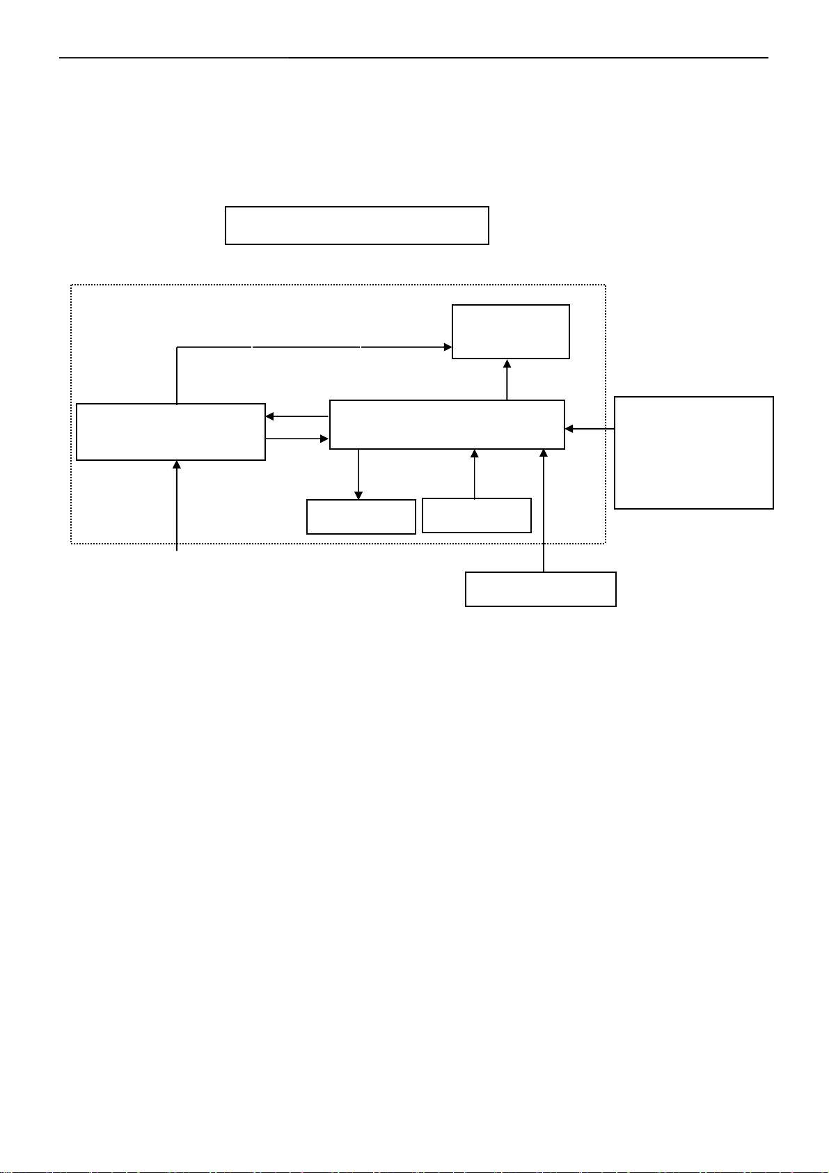
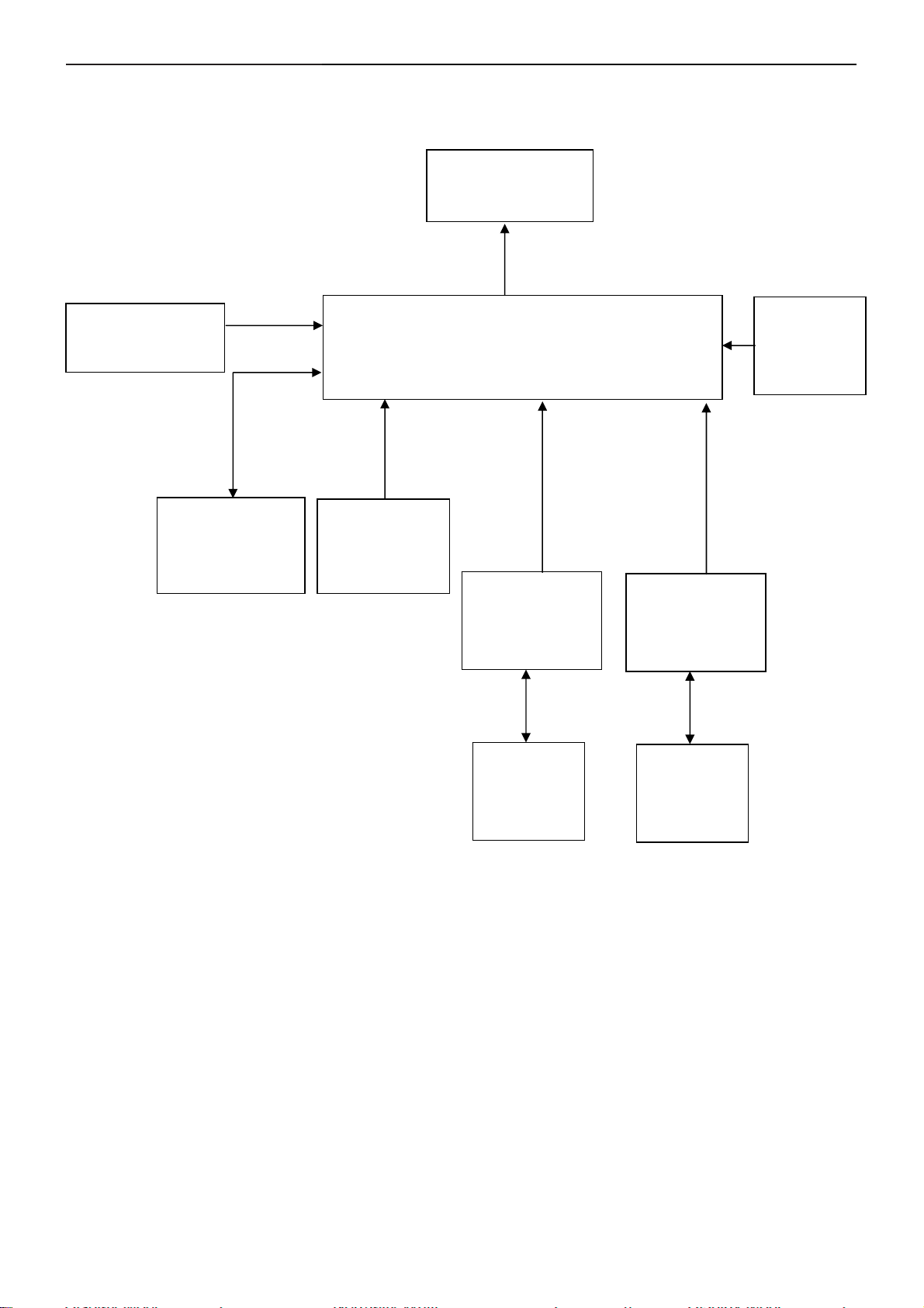
2. LCD Monitor Description
The LCD monitor will contain a main board, an audio board, a power board and a key board which house the flat
panel control logic, brightness control logic and DDC.
The power board will provide AC to DC Inverter voltage to drive the backlight of panel and the main board chips
each voltage.
Power board
Include: adapter, inverter)
AC-IN
100V-240V
Monitor Block Diagram
CCFL Drive.
Audio Board
Flat Panel and
CCFL backlight
Main Board
Key Board
HOST Computer
RS232 Connector
For white balance
adjustment in factory
mode
Video signal, DDC
http://www.wjel.net
5
17" LCD Color Monitor ASUS VB171T&S
3. Operating Instructions
3.1 General Instructions
Press the power button to turn the monitor on or off. The other control buttons are located at the front of the
panel of the monitor.
By changing these settings, the picture can be adjusted to your personal preferences.
The power cord should be connected.
-
Connect the video cable from the monitor to the video card.
-
Press the power button to turn on the monitor, the power indicator will light up.
-
3.2 Control Buttons
3.2.1 Key Control
http://www.wjel.net
6
17" LCD Color Monitor ASUS VB171T&S
3.2.2 Key Function
3.3 OSD Menu
3.3.1 How to Reconfigure
http://www.wjel.net
7
17" LCD Color Monitor ASUS VB171T&S
3.3.2 OSD Function Introduction
http://www.wjel.net
8
17" LCD Color Monitor ASUS VB171T&S
http://www.wjel.net
9
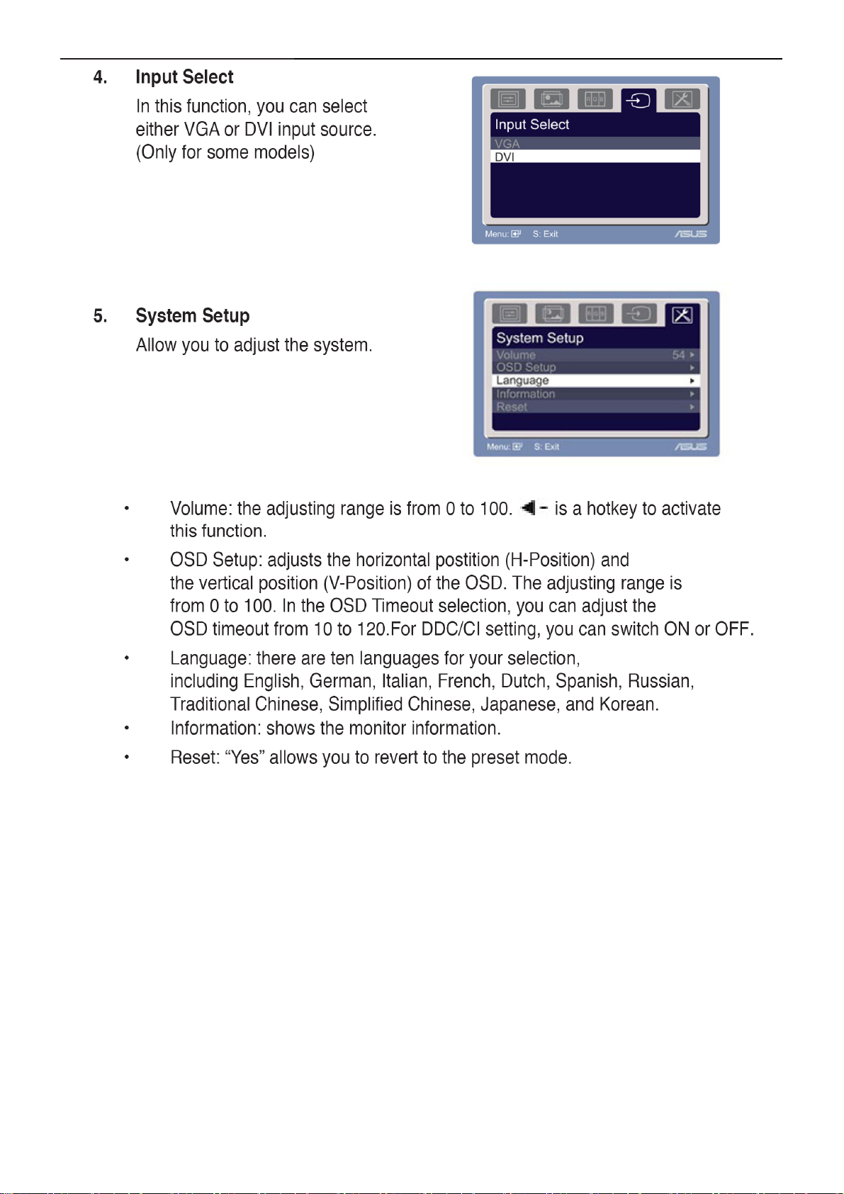
17" LCD Color Monitor ASUS VB171T&S
http://www.wjel.net
10
17" LCD Color Monitor ASUS VB171T&S
4. Input/Output Specification
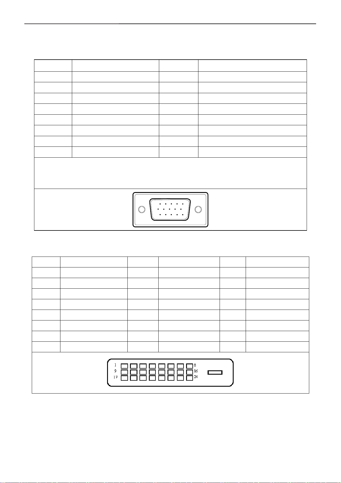
4.1 Input Signal Connector
Analog connectors
Pin No. Description Pin No. Description
1. Red Video 9. +5V
2. Green Video 10. Logic Ground
3. Blue Video 11. Monitor Ground
4. Monitor Ground 12. DDC-Serial Data
5. DDC-Return 13. H-Sync
6. Red Ground 14. V-Sync
7. Green Ground 15. DDC-Serial Clock
8. Blue Ground
VGA connector layout
15
6
11 15
DVI connectors
Pin No. Description Pin No. Description Pin No. Description
1. RX2- 9. R X1- 17. RX0-
2. RX2+ 10. RX1+ 18. RX0+
3. RX2 Shield 11. RX1 Shield 19. RX0 Shield
4. NC 12. NC 20. NC
5. NC 13. NC 21. NC
6. DDC Clock 14. +5V Power 22. RX Clock Shield
7. DDC Data 15. Ground 23. RX Clock+
8. NC 16. Hot Plug Detection 24. RX Clock-
http://www.wjel.net
10
11
17" LCD Color Monitor ASUS VB171T&S
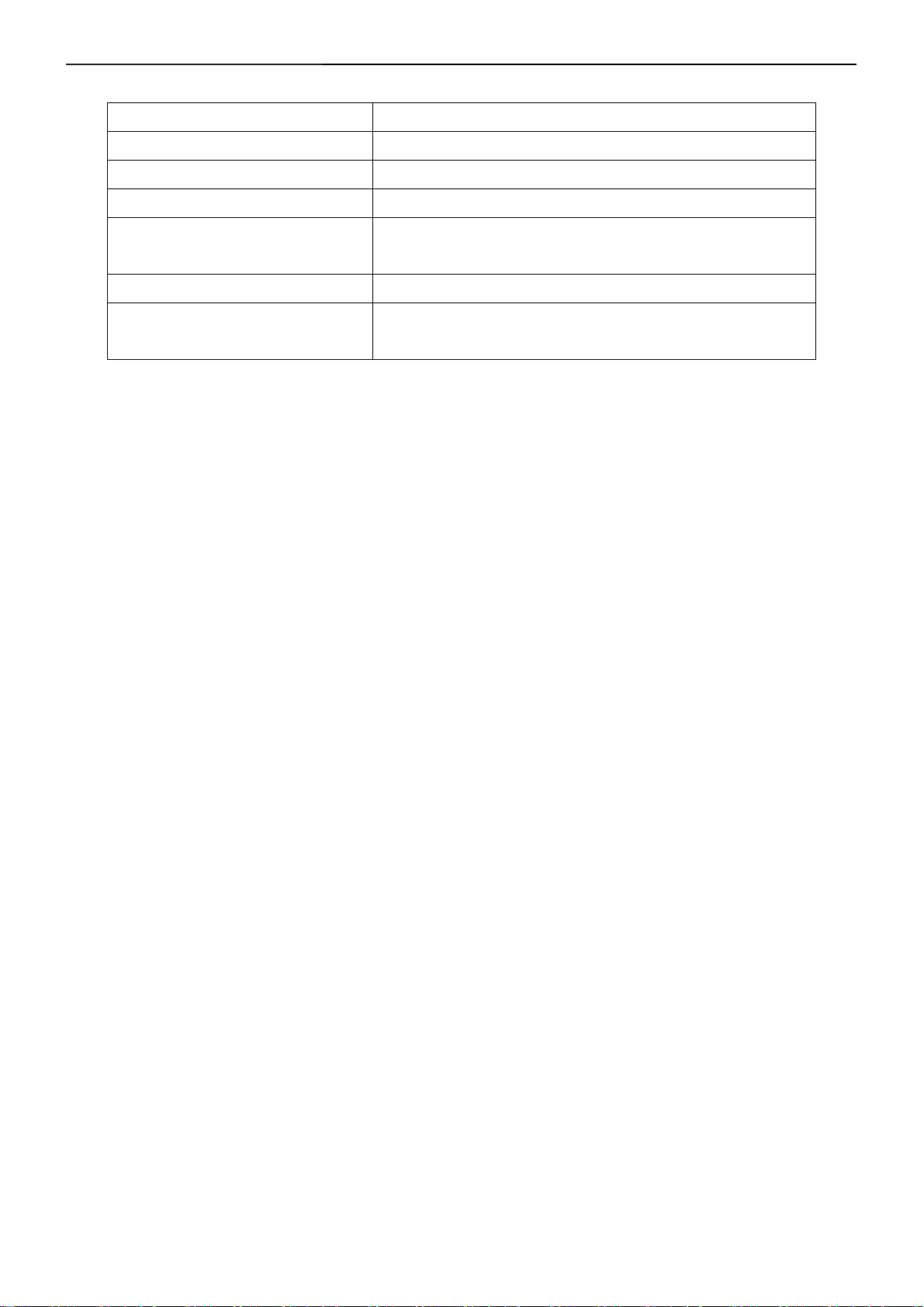
4.2 Power Supply Requirements
A/C Line voltage range 100 V ~ 240 V
A/C Line frequency range
Input Voltage transients
Current 1.5A max at 100V; 0.8A max at 240 V
Peak surge current
Leakage current < 3.5mA
Power line surge
50 ± 3Hz, 60 ± 3Hz
90-264 voltage AC for 10 sec @40℃
< 60A peak at 240 VAC and cold starting
< 30A peak at 120VAC and cold starting
No advance effects (no loss of information or defect)
with a maximum of 1 half-wave missing per second
http://www.wjel.net
12
17" LCD Color Monitor ASUS VB171T&S
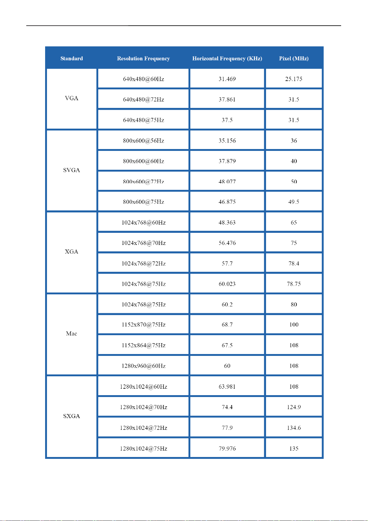
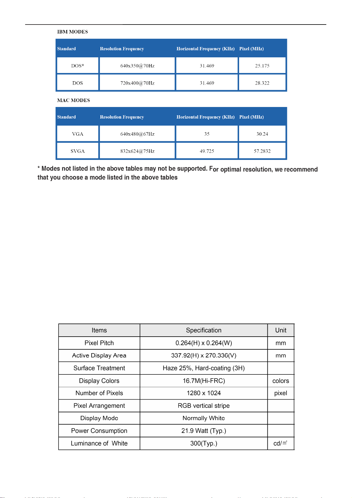
4.3 Factory Preset Display Modes
http://www.wjel.net
13
17" LCD Color Monitor ASUS VB171T&S
4.4 Panel Specification
4.4.1 Features
RoHS compliance (Pb-free)
High contrast ratio, high aperture ratio, fast response time
TN(Twisted Nematic) mode
2 dual CCFTs(Cold Cathode Fluorescent Tube)
DE(Data Enable) mode
LVDS (Low Voltage Differential Signaling) interface (2pixel/clock)
COMPACT SIZE DESIGN
TCO’03 compliance
4.4.2 Display Characteristics
http://www.wjel.net
14
17" LCD Color Monitor ASUS VB171T&S
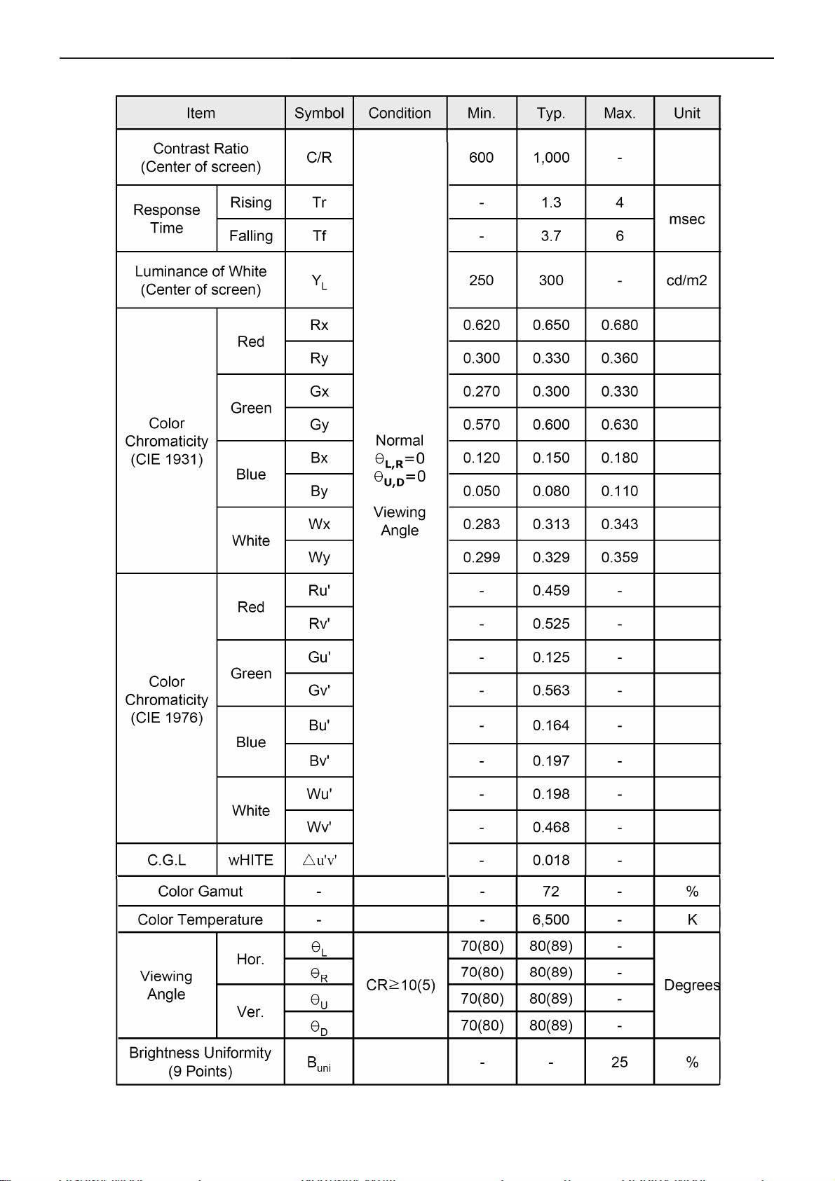
4.4.3 Optical Characteristics
http://www.wjel.net
15
17" LCD Color Monitor ASUS VB171T&S
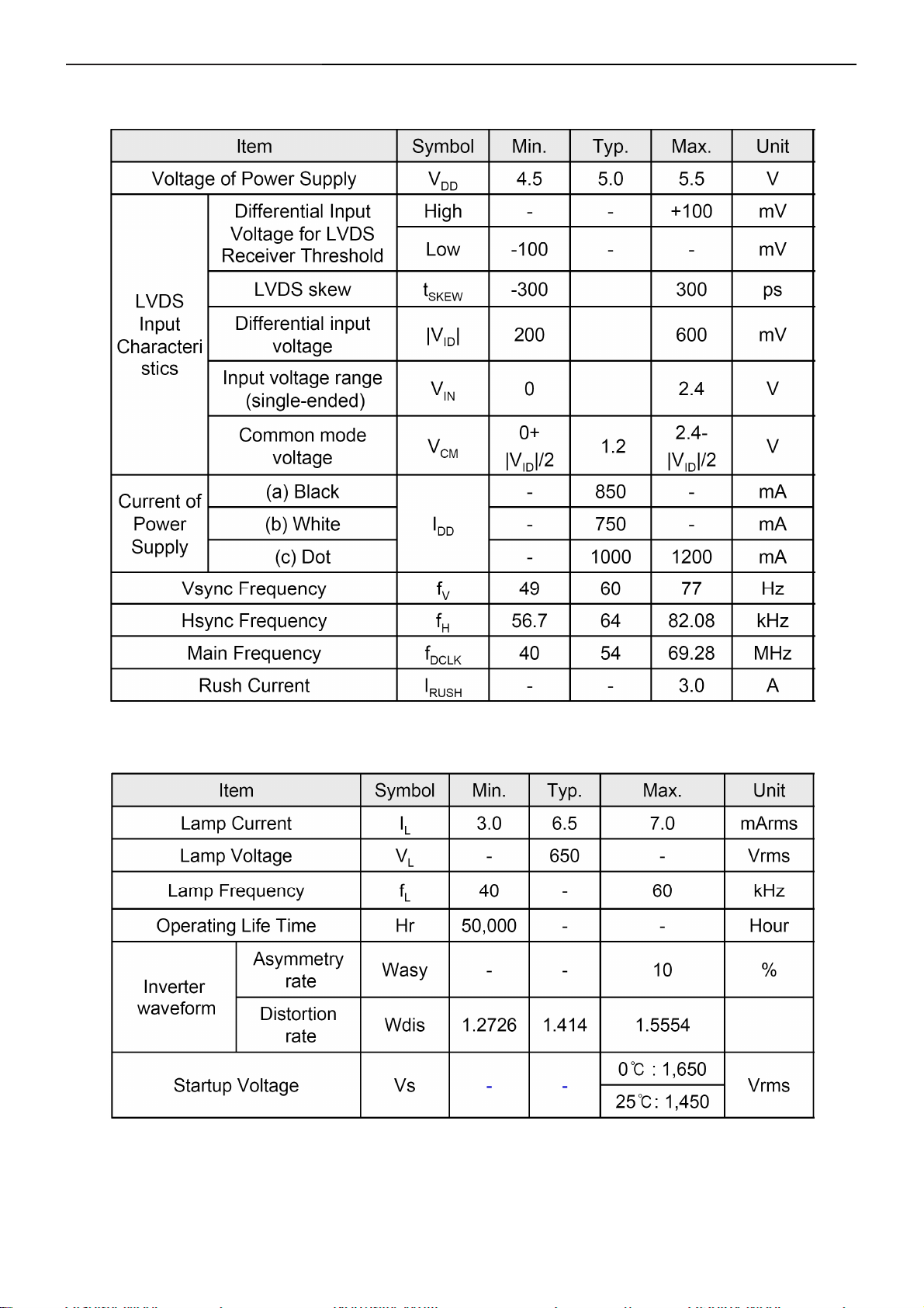
4.4.4 Electrical Characteristics
(1) TFT-LCD
(2) Backlight
http://www.wjel.net
16
17" LCD Color Monitor ASUS VB171T&S
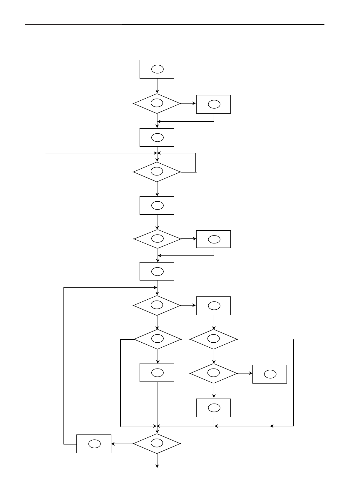
5. Block Diagram
5.1 Software Flow Chat
1
2
N
4
5
Y
6
7
Y
Y
N
N
3
9
10
Y
N
12
Y
N
11
13
N
Y
http://www.wjel.net
N
16
18
14
N
19
15
Y
17
Y
17

17" LCD Color Monitor ASUS VB171T&S
1) MCU initialize.
2) Is the EPROM blank?
3) Program the EPROM by default values.
4) Get the PWM value of brightness from EPROM.
5) Is the power key pressed?
6) Clear all global flags.
7) Are the AUTO and SELECT keys pressed?
8) Enter factory mode.
9) Save the power key status into EPROM.
Turn on the LED and set it to green color.
Scalar initializes.
10) In standby mode?
11) Update the lifetime of back light.
12) Check the analog port, are there any signals coming?
13) Does the scalar send out an interrupt request?
14) Wake up the scalar.
15) Are there any signals coming from analog port?
16) Display "No connection Check Signal Cable" message. And go into standby mode after the message
disappear.
17) Program the scalar to be able to show the coming mode.
18) Process the OSD display.
19) Read the keyboard. Is the power key pressed?
http://www.wjel.net
18
17" LCD Color Monitor ASUS VB171T&S
_
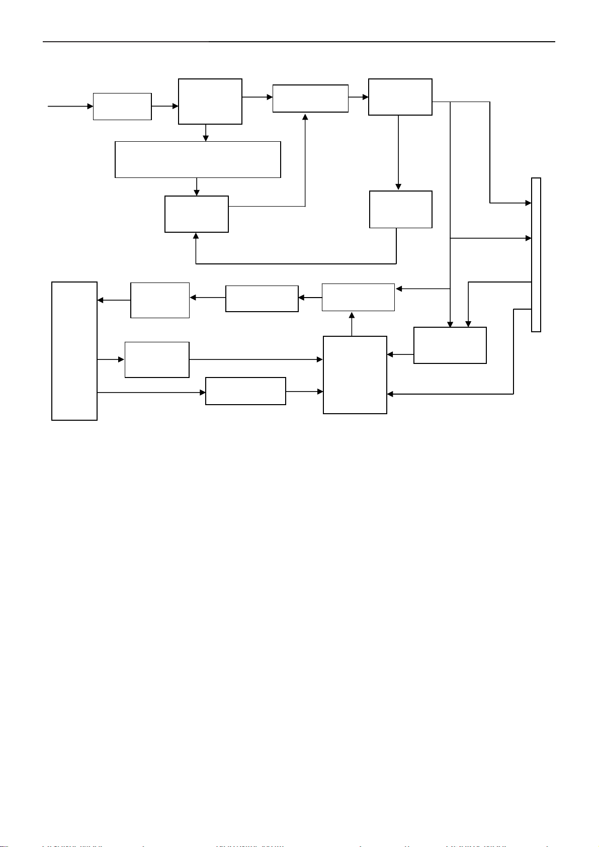
5.2 Electrical Block Diagram
5.2.1 Main Board
Keypad Interface
(CN404)
SDA
SCL
Flash Memory
PM25LV010A
(U402)
Crystal
14.31818MHZ
(X401)
Panel Interface
(CN703)
Scalar TSUM56AWHK-LF
(Include MCU, ADC, OSD)
(U401)
H sync
V sync
RGB
D-Data
D-Clock
EEPROM
M24C02
(U406)
D-Sub
Connector
(CN401)
DVI
Connector
(CN402)
VGA_SDA,
VGA_SCL
DVI_SDA,
DVI
SCL
EEPROM
M24C02
(U403)
EEPROM
M24C02
(U404)
http://www.wjel.net
19
17" LCD Color Monitor ASUS VB171T&S
t
t
5.2.2 Inverter/Power Board
AC input
EMI filter
Bridge
Rectifier
and Filter
Transformer
Rectifier
diodes
Start Circuit: R904, R932, R933
CN902
PWM
Control IC
Feedback
Circuit
12V
5V
ON/OFF
Lamp
Output
Circui
Feedback
Circui
Transformer MOSFET
Control IC
Over Voltage
(IC801)
PWM
ON/OFF
Control
DIM
http://www.wjel.net
20
17" LCD Color Monitor ASUS VB171T&S
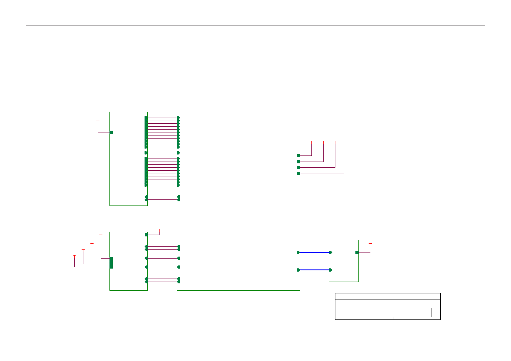
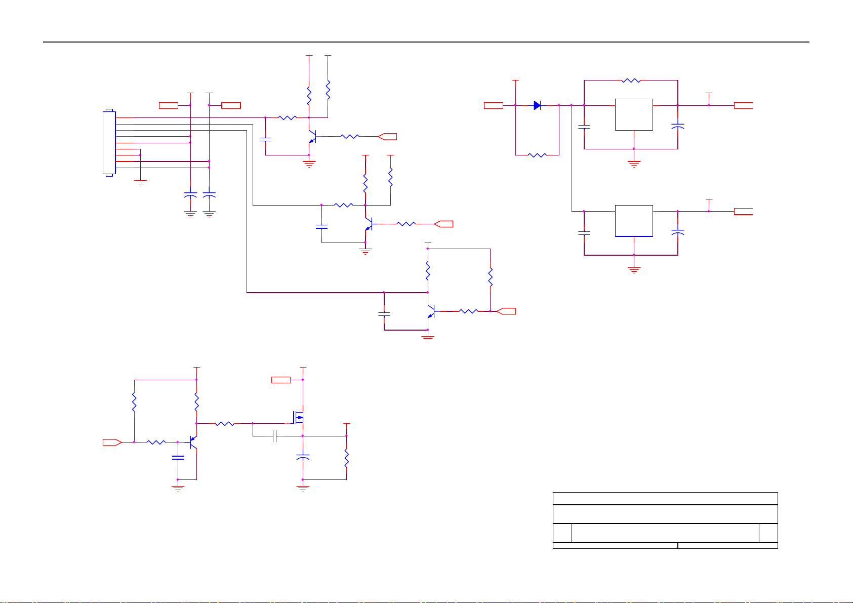
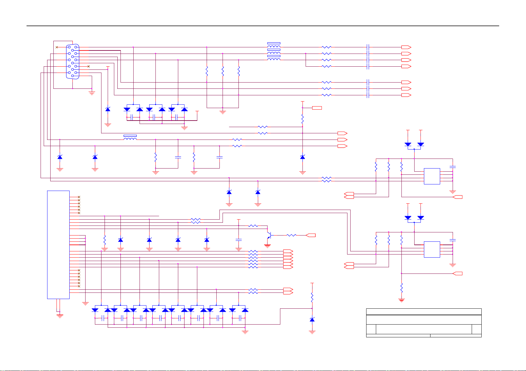
6. Schematic
6.1 Main Board
715G2571-1-2
TSUM56AHK SCHEMATIC
VCC3.3
XGA/SXGA/WSXGA
B3
+5V
+5V
RIN
GNDR
GNDG
SOG
BIN
GNDB
HSYNC
VSYN C
DDCA_SDA
DDCA_SCL
INPUT_DET
CLK+
CLK-
DDCD_SDA
DDCD_SCL
DDC_WP
HDCP_RST
GIN
R+
RG+
G-
B+
B-
B4
RIN
GNDR
GIN
GNDG
SOG
BIN
GNDB
HSYNC
VSYN C
DDCA_SDA
DDCA_SCL
INPUT_DET
R+
R-
G+
GB+
BCLK+
CLK-
DDCD_SDA
DDCD_SCL
DDC_WP
HDCP_RST
LVDS OUTPUT
VCC3.3
VCC1. 8
+5V
+12V
VCC1.8
VCC3.3 +12V
+5V
3.INP UT
B2
+12V
VCC1.8
+5V
+12V
VCC1. 8
+5V
VCC3. 3
VLCD
on_BACKLIG HT
on_Panel
Adj_BL2
Adj_BACKLIG HT
I2C_MCL
I2C_MDA
VLCD
on_BACKLIG HT
on_Panel
Adj_BL2
Adj_BACKLI GHT
I2C_MCL
I2C_MDA
PA[0..9]
PB[0..9]
PA[0..9]
PB[0..9]
B5
VLCD
VLCDPA[0.. 9]
PB[0.. 9]
5.PANEL INTERFACE
2.PO WER
4.SCALER
http://www.wjel.net
Tit le
Size Do cument Num ber Rev
B
Date: Sheet
1.2 TOP
715G2571-1-2
of
1.2 6Saturday , April 14, 2007
A
21
17" LCD Color Monitor ASUS VB171T&S
VCC3.3
+5V
SOT-223
R707 NC
U701
3 2
VI VO
C705
0.1uF /16V
SOT-223
U702
3 2
VI VO
C707
0.1uF /16V
VCC3.3
VCC 3.3 4
C706
GND
1
GND
1
+
+
10uF/ 50V
VCC1.8
C708
10uF/ 50V
VCC 1.8 4
CN701
CONN
NC
+5V
+12V
C701
100uF 50V
+12V 4
+5V3, 4
1
2
3
4
5
6
7
8
9
C702
100uF/ 25V
+
+
C703
NC
R701
R702
47R 1/ 16W
(
1uF 10V
R720
1K 1/16W
R703 4K7 1/16W
)
Q701
PMBS3904
R717
NC
C713
NC
+5V
VCC3.3
R716
NC
R715 NC
Q705
NC
Adj_BACKLIGH T 4
R721
NC
+5V
+5V3, 4
Adj_BL2 4
+5V
D701
SMAL140
R706
NC
R704
10K 1/16W
C704
0.1uF /16V
C710
VLCD
Q703
AO3401
+
C711
10uF/50V
+5V
R712
10KΩ 1/10W
+5V
VLCD5
R708
10K 1/16W
on_Panel4
R709
4K7 1/16W
0.1uF/ 16V
C709
R710
10K 1/16W
R711
51K 1/16W
Q704
PMBS3906
0.1uF /16V
R705 4K7 1/16W
Q702
PMBS3904
R718
10K 1/16W
on_BACKLI GHT 4
http://www.wjel.net
Tit le
Size Document Number Rev
B
Date: Sheet
2.Power
715G2571-1-2
A
26Saturday, April 14, 2007
of
22
17" LCD Color Monitor ASUS VB171T&S
7
CN402
SYNC GND
JACK
11
12
13
14
15
DB15
HSI
VSI
ZD403
MM3Z5V6B
RGB GND
HSYNC
VSYN C
DDC SCL
DDC SDA
+5V
HPD
1/3shield
2/4shield
0/5shield
clk shield
DAT0+
DAT0DAT1+
DAT1DAT2+
DAT2DAT3+
DAT3DAT4+
DAT4DAT5+
DAT5-
clk+
clk-
GND
GND
32
31
1
16
25
R
26
G
27
B
29
28
8
15
6
7
14
16
11
3
19
22
18
17
10
9
2
1
13
12
5
4
21
20
23
24
1
6
2
7
3
8
4
9
5
10
RED+
REDGREEN+
GREENBLUE+
BLUE-
PC5V
VGA_CON
MM3Z 5V6B
ZD404
MM3Z 5V6B
SCL_DVI
SDA_DVI
DVI5V
HPD
DAT0+
DAT0DAT1+
DAT1DAT2+
DAT2-
DCLK+
DCLK-
C416
2
0.1uF/16V
swit ching diode BAV99
PC5V
ZD402
swit ching diode BAV99
FB404 120 OHM
ZD407
R423
NC
MM3Z 5V6B
3
3
D404
C417
2
1
0.1uF /16V
switching diode BAV99
3
D401
C401 0.1u F/16V
1
2
DET_DVI
3
D405
C418
2
1
0.1uF/16V
3
D402
C402 0.1uF/16V
1
2
R413
2K2 1/16W
ZD408
MM3Z5V6B
3
D406
D407
C419
1
2
0.1uF/16V
switching diode BAV99
FB401 0R05 1/10W
FB402 0R05 1/10W
FB403 0R05 1/10W
R401
R402
75 1/16W
3
D403
ESD_5V
C403 0.1uF/ 16V
1
2
swit ching diode BAV99
C411
33pF
ZD409
MM3Z5V6B
3
D408
http://www.wjel.net
C420
1
2
1
0.1uF /16V
switching diode BAV99
switching diode BAV99
swit ching diode BAV99
R415
2K2 1/16W
R427 51R 1/16W
R425
51R 1/16W
ZD410
MM3Z5V6B
3
D409
C421
1
2
0.1uF/16V
R414 1K 1/16W
R416 1K 1/16W
C412
220pF
ZD405
MM3Z5V6B
3
D410
C422
1
2
0.1uF /16V
switching diode BAV99
switching diode BAV99
R403
75 1/16W
DET_DVI
DVI5V
R430 10K 1/16W
C415
0.1uF /16V
R432 10R 1/16W
R433 10R 1/16W
R434 10R 1/16W
R435 10R 1/16W
R436 10R 1/16W
R437 10R 1/16W
R438 10R 1/16W
R439 10R 1/16W
3
C423
1
2
0.1uF/16V
75 1/16W
R424
2.2KΩ 1% 1/16W
R412
1K 1/16W
ZD406
MM3Z5V6B
D411
switching diode BAV99
Q401
PMBS3904
ZD401
SCL_VGA
SDA_VGA
R431
4K7 1/16W
B+ 4
B- 4
G+ 4
G- 4
R+ 4
R- 4
CLK+ 4
CLK- 4
ESD_5V
+5V
R411
4.7KΩ 1% 1/16W
MM3Z5V6B
ZD411
MM3Z5V6B
R404
56Ω 1% 1/16W
R406
56Ω 1% 1/16W
R408
56Ω 1% 1/16W
R410 470R 1/ 16W
R405 100R 1/ 16WCN401
R407 100R 1/ 16W
R409 100R 1/ 16W
+5V 2, 4
R419
R417
DDCA_SDA4
DDCA_SCL4
HDCP_RST 4
DDCD_SDA4
DDCD_SCL4
+5V
R440
1K 1/16W
51R 1/16W
51R 1/16W
C404 0.047uF
C406 0.047uF
C408 0.047uF
C410 0.047uF
C405 0.047uF
C407 0.047uF
C409 0.047uF
INPUT_DET 4
HSYNC 4
VSYN C 4
4K7 1/16W
R426
R420
R428
4K7 1/16W
R418
4K7 1/16W
4K7 1/16W
Tit le
Size Document Number Rev
B
Date: Sheet
RIN 4
GIN 4
BIN 4
SOG 4
GNDR 4
GNDG 4
GNDB 4
PC5V
+5V
1
2
3
R421
8
10K 1/16W
7
6
M24C 02- WMN6 TP
DVI5V
+5V
1
2
3
R429
8
10K 1/16W
7
6
M24C 02- WMN6 TP
R450
NC
3.INPUT
715G2571-1-2
D412
BAV70
U403
VCC
WP
SCL
D413
BAV70
U404
VCC
WP
SCL
A0
A1
A2
VSSSDA
A0
A1
A2
VSSSDA
1
2
3
45
1
2
3
45
36Saturday , April 14, 2007
C413
0.22uF 16V
DDC_WP 4
C414
0.22uF 16V
DDC_WP 4
of
A
23
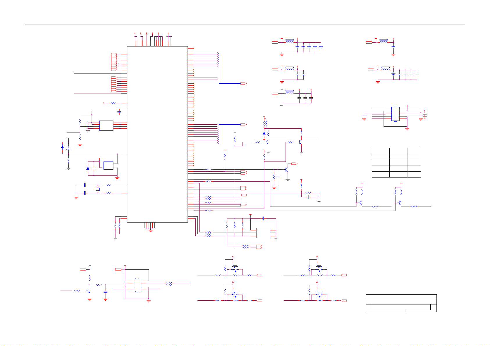
17" LCD Color Monitor ASUS VB171T&S
VPLL
D414
LL4148
Reset Circuit 2
VOLUME
SF_WP
+5V
+
R445
10K 1/16W
SDA_DB
SCL_DB
SDA_DVI
SCL_DVI
R443
NC
R444
10K 1/16W
C426
10uF/50V
ZD412
NC
Reset Circuit 1
C428 22pF
C429 22pF
+5V2, 3
R484 4K7 1/16W
3
AVDD
VCC3.3
8
7
3
C425
0.22uF16V
4 5
+5V
NC
C427
1 2
X401
14.3 Mhz
1 2
+5V
R485
1K 1/16W
R486 10K 1/16W
Q405
PMBS3904
RIN3
GNDR3
GIN3
GNDG3
SOG3
BIN3
GNDB3
HSYNC
VSYN C3
R+3
R-3
G+3
G-3
B+3
B-3
CLK+3
CLK-3
R442
390 1/16W
U402
SDO
VDD
CE#
HOLD#
WP#
SCK
VSS SDI
PM25LV010A
U405
RESET
3
GND
VCC
NC
R446 22R 1/16W
R447 22R 1/16W
R449
10K 1/16W
+12V2
C450
1uF 10V
C424
0.1uF/16V
2
1
6
2
1
XIN
XOU T
OUT-L+
59
58
56
55
57
54
53
63
64
65
66
39
40
42
43
45
46
48
49
36
37
51
62
61
70
71
72
73
19
32
33
102
104
R451
10K 1/16W
+12V
VDVI
RIN0P
RIN0M
GIN0P
GIN0M
SOGIN0
BIN0P
BIN0M
HSYNC0
VSYN C0
DDCA_SDA
DDCA_SCL
R+
RG+
GB+
BCK+
CKDDCD_SDA
DDCD_SCL
REXT
REFP
REFM
SDO
CSZ
SCK
SDI
RST
XIN
XOU T
MODE [0]
MODE [1]
1
3
5
7
9
44
CN403
CONN
VMPLL
50
52344
BYPASS
AVDD_DVI
AVDD_DVI
AVDD_PLL
AVDD_MPLL
GND
GND
3896116
13
2
4
6
8
10
VDDC
VDDP
AVDD
VCC3.3
VDDP
AUDIO_STBY
1
2
3
45
VCC3.3
VCC3.3
C446
0.1uF/16V
FB407
600 OHM
FB408
600 OHM
FB409
600 OHM
R482
10KΩ 1/16W
SCL_DB
SDA_DB
Q402
PMBS3904
C430
0.047uF
VDVI
C436
0.1uF/16V
VMPLL
C439
0.1uF/16V
DDC_WP 3
+5V
4K7 1/16W
R499
47R 1/16W
4K7 1/16W
R503
47R 1/16W
C431
C432
0.047uF
33pF
C437
0.1uF/16V
VPLL
C440
0.1uF/16V
R481
20KΩ 1/16W
AUDIO_MUTE
Q412
2N3904S-RTK/PS
20070308
R458
10K 1/16W
R459 20K 1/16W
C447 0.1uF/16V
R500
R504
C433
C434
220pF
220pF
C438
0.1uF/16V
+5V
R501 NC
+5V
Q408
2N7002E
Q409
2N7002E
R502
47R 1/16W
R506
47R 1/16W
1K 1/16W
DDCA_SCL 3
DDCA_SDA 3
R465
14
60
AVDD_ADC
GND
GND
GND
41
47
OUT-R+
68
97
95
103
115
117
TSUM56AWHK-LF
11
VCTRL
107
GPIO_P23
GPIO_P22
GPIO_P12
RSTN
GPIO_P03
GPIO_P06
GPIO_P07
GPIO_P13
GPIO_P14
PA0
108
PA1
109
PA2
PA3
110
111
PA4
112
PA5
113
PA6
114
PA7
98
NC
99
NC
100
NC
101
NC
105
PA8
106
PA9
89
NC
90
NC
91
NC
92
NC
93
NC
94
NC
9
10
15
16
17
18
2
3
5
6
7
8
PB0
118
119
PB1
PB2
120
PB3
121
122
PB4
123
PB5
124
PB6
125
PB7
126
PB8
PB9
127
128
1
80
NC
81
NC
88
NC
87
NC
86
NC
85
NC
84
NC
83
NC
82
NC
74
R456 22K 1/16W
35
69
78
79
R464 4K7 1/16W
75
20
21
22
23
24
R461 100R 1/16W
25
R462 100R 1/16W
26
27
R460 100R 1/16W
28
29
30
31
R468 4K7 1/16W
77
76
R472 100R 1/16W
R474 100R 1/16W
R476 100R 1/16W
SCL_DVI
SDA_DVI
PA[0..9]
PB[0..9]
VCC3.3
R454
NC
SF_WP
KEY1
KEY2
POWER
VOLUME
R492
4K7 1/16W
R491
47R 1/16W
R493 NC
R496
4K7 1/16W
R495
47R 1/16W
R497 NC R505 NC
PA[0..9] 5
PB[0..9] 5
+5V
R719
NC
HDCP_RST 3
Adj_BL2 2
on_BACKLIGHT 2
adj_BACKLIGHT 2
INPUT_DET 3
on_PANEL 2
VCC3.3
R475
R473
R477
10K 1/16W
10K 1/16W
R512 NC
R511 NC
+5V
Q406
2N7002E
R494
47R 1/16W
+5V
Q407
2N7002E
R498
47R 1/16W
VDDP
VDDP
VDDP
VDDP
VDDP
VDDC
VDDC
VDDC
VDDC
NC/LV ACKP/NC
NC/LVACKM/NC
RA1P/LVA2P/R A2
RA1N/LVA2M/R A3
RA2P/LVA1P/R A4
RA2N/LVA1M/R A5
RA3P/LVA0P/R A6
RA3N/LVA0M/R A7
GA3P/LVA3P/GA6
GA3N/LVA3M/GA7
RB1P/NC/RB2
RB1N/NC/RB3
RB2P/NC/RB4
RB2N/NC/RB5
RB3P/NC/RB6
RB3N/NC/RB7
GB1P/NC/ GB2
GB1N/NC /GB3
GB2P/NC/ GB4
GB2N/NC /GB5
GB3P/NC/ GB6
GB3N/NC /GB7
CLKAP/LVB3P/LHSY NC
CLKAN/LVB3M/LVSYN C
CLKBP/LVBCKP/LCK_OD D
CLKBN/ LVBCKM/LD E
NC/LVB2P/NC
NC/LVB2M/NC
BB1P/LVB1P/ BB2
BB1N/LVB1M/BB3
BB2P/LVB0P/ BB4
BB2N/LVB0M/BB5
BB3P/NC/BB6
BB3N/NC/ BB7
GPIO_P16/PWM2
GPIO_P15/PWM0
PWM2/GPIO _P24
GPIO_P27/PWM1
PWM1/GPIO _P25
GPIO_P00/SAR1
GPIO_P01/SAR2
GPIO_P02/SAR3
PWM0/GPIO _P26
GPIO_P10/I2C _MCL
GPIO_P11/I2C _MDA
GND
RSDS/LVDS/TTL
1K 1/16W
R518
AUDIO _STBY
AUDIO _MUTE
http://www.wjel.net
R516
1K 1/16W
U40 1
67
12
3.9KΩ 1/16W
10K 1/16W
ZD413
MM3Z5 V6B
R479
10K 1/16W
8
7
6
+12V
R478
+5V
R514
10K 1/16W
VCC
WP
SCL
M24C16
I2C_MCL 2
I2C_MDA 2
DDCD_SCL 3
DDCD_SDA 3
VCC3. 32
VCC3. 32
VCC3. 32
R483
3.9KΩ 1/16W
R480
20KΩ 1/16W
Q411
2N3904S-RTK/PS
NC
R457
C448
0.22uF
U406
A0
A1
A2
GNDSD A
VCC3.3
VCC3. 32
VCC1. 82
LED_G
C451
1000pF
+5V
R466
240Ω 1/16W
Q403
PMBS3906
Titl e
Size Document Number Rev
C
Date: Sheet
AVDD
FB406
600 OHM
VDDC
VCC1.8
FB405
1 2
0 ohm
C441
10uF/50V
OUT-L+
2
4
6
8
POWER
10
KEY2
12
KEY3
New Key port define
INPUT_D ET
Pull-High
D_Sub
Only
DVI
Only
Both
connected
Both Not
connected
R469
1K 1/16W
LED_G
R467
680R 1/16W
C435
0.047uF
+
C442
0.047uF
CN404
1
3
5
7
9
11
CONN
4.7K 1/16W
1K 1/16W
2.2K 1/16W
+5V
Q404
4.SCALER
715G2571-1-2
C443
0.047uF
VCC3.3
R470
240Ω 1/16W
PMBS3906
C445
0.047uF
OUT-R+
LED_A
KEY1
Detect
Voltage
0.877 V
1.594 V
0.638 V
5 V
C444
0.047uF
C452
R471
680R 1/16W
46Saturday , April 14, 2007
LED_A
of
1000pF
C453
1000pF
A
24
 Loading...