

Page 1
華華碩碩電電腦
腦
GTC ■ Service Manual
ASUS P550 Level 3 4
Trouble shooting Guide
Page 2

華華碩碩電電腦
腦
GTC ■ Service Manual
Context
1. Feature Introduction ........................................................................................................................................... 3
ID Overview ................................................................................................................................................... 3
Main key function Description....................................................................................................................... 4
2. Block Diagram ................................................................................................................................................... 5
3.1 Solaris TOP View..................................................................................................................................... 6
3.2 Solaris Bottom View ................................................................................................................................ 7
4. Base Band Repair Tooling.................................................................................................................................. 8
4.1 HW ........................................................................................................................................................... 8
5. Chip Timing Sequence ..................................................................................................................................... 10
5.1 PMU Timing Sequence .......................................................................................................................... 10
5.2 CPU Timing sequence ............................................................................................................................ 11
5.3 System Flowchart ................................................................................................................................... 12
5.4 Power supply Block................................................................................................................................ 13
5.5 Power system Supplied Block................................................................................................................ 14
5.6 Power System Charging block ............................................................................................................... 14
6. Trouble shooting............................................................................................................................................... 15
6.1 General Process ...................................................................................................................................... 15
6.2 Can’t Power ON process ........................................................................................................................ 16
7. Trouble shooting............................................................................................................................................... 18
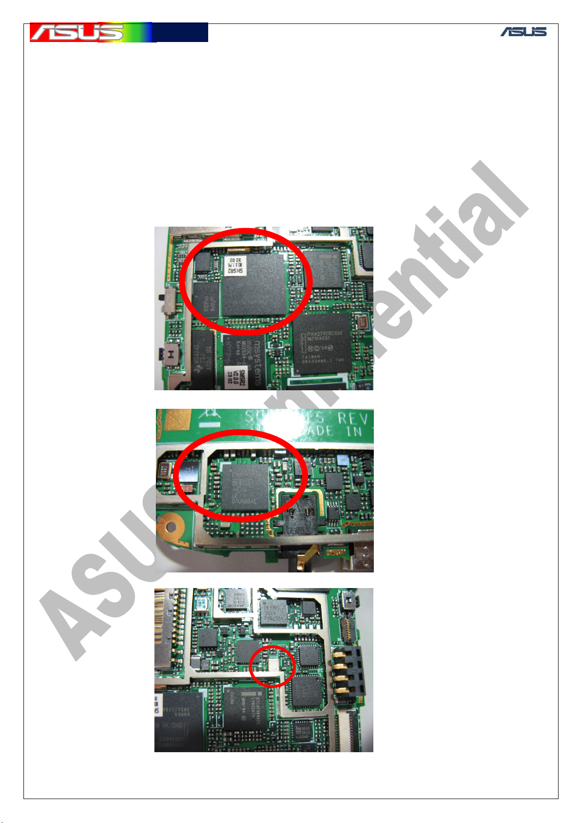
7.1 Touch panel failed .................................................................................................................................. 18
7.2 SDRAM.................................................................................................................................................. 19
7.3 Flash failed ............................................................................................................................................. 20
7.4 SDCARD................................................................................................................................................ 20
7.5 WiFi failed.............................................................................................................................................. 22
7.6 Modem-BUS failed ................................................................................................................................ 23
7.7 SIM failed............................................................................................................................................... 24
7.8 LED ........................................................................................................................................................ 24
7.9 Display failed.......................................................................................................................................... 25
7.10 Battery failed ........................................................................................................................................ 26
7.11 Vibrator failed....................................................................................................................................... 27
7.12 Camera.................................................................................................................................................. 27
7.13 Button failed ......................................................................................................................................... 28
7.14 BT failed............................................................................................................................................... 29
7.15 Audio failed .......................................................................................................................................... 29
Speaker no sound.................................................................................................................................. 29
Receiver no sound ................................................................................................................................ 30
Headphone no sound ............................................................................................................................ 31
Headphone MIC no record ................................................................................................................... 32
7.16 Standby current failed........................................................................................................................... 33
8. RF Repair Requirement............................................................................................................................ 34
8.1 SW: ...................................................................................................................................................... 34
8.2 HW: ..................................................................................................................................................... 34
8.3 Equipment: .......................................................................................................................................... 34
9. Block Diagram ................................................................................................................................................. 35
9.1 System Block Diagram........................................................................................................................... 35
9.2 GSM/GPRS – GSM RFMD solaris I Block Diagram............................................................................ 36
9.3 WCDMA – Maxim 3G Block Diagram.................................................................................................. 37
9.4 Blue tooth – CSR BC04 ......................................................................................................................... 38
9.5 WIFI– UGGZ3X10BA ........................................................................................................................... 39
9.6 GPS– GSC3F/LP-7................................................................................................................................. 40
10.1 Backside Antenna Area Test Points...................................................................................................... 41
10.2 GSM/GPRS Test Points........................................................................................................................ 42
10.3 WCDMA Test Points............................................................................................................................ 43
1
Page 3

華華碩碩電電腦
腦
11. GSM & WCDMA RF Tx/Rx Path.................................................................................................................. 44
11.1 GSM Tx path ........................................................................................................................................ 44
11.2 GSM Rx path........................................................................................................................................ 44
11.3 WCDMA Tx path ................................................................................................................................. 45
11.4 WCDMA Rx path ................................................................................................................................. 45
12. Test & Repair Flow Chart............................................................................................................................... 47
12.1 Conductive & Antenna Test Procedure ................................................................................................ 47
12.3 WCDMA Test & Repair Procedure ...................................................................................................... 49
12.4 Blue tooth Test & Repair Procedure..................................................................................................... 50
12.5 WIFI Test & Repair Procedure............................................................................................................. 51
13. Test Points Signal Examples .......................................................................................................................... 52
13.1 GSM900 ............................................................................................................................................... 52
13.2 DCS1800 .............................................................................................................................................. 55
13.3 PCS1900............................................................................................................................................... 58
13.4 WCDMA .............................................................................................................................................. 61
14. Blue tooth ....................................................................................................................................................... 67
15. WIFI ............................................................................................................................................................... 71
16. Appendix ........................................................................................................................................................ 75
16.1 Typical Value of GSM/GPRS Conductive Tx/Rx Test......................................................................... 75
16.2 Typical Value of WCDMA Conductive Tx/Rx Test ............................................................................. 75
16.3 Tx Test Environment Setup .................................................................................................................. 76
16.4 Rx Test Environment Setup.................................................................................................................. 77
17. GPS Introduce Purpose: ................................................................................................................................. 78
17.1 Equipment requires............................................................................................................................... 78
17.2 Software: .............................................................................................................................................. 78
17.3 Hardware: ............................................................................................................................................. 78
18. GPS Test points & Schematic......................................................................................................................... 79
18.1 GPS Active Path................................................................................................................................... 79
18.2 Passive Path.......................................................................................................................................... 80
18.3 GPS Chip.............................................................................................................................................. 80
18.4 Power part test points ........................................................................................................................... 81
18.5 Testing signal from base band .............................................................................................................. 81
19. Test points placement point ............................................................................................................................ 82
19.1 GPS Antenna ........................................................................................................................................ 82
20. GPS Hardware Examination Procedure ................................................................................................. 83
21. Measurement results of all test points ............................................................................................................ 87
22. Software procedure......................................................................................................................................... 89
22.1 GPS firmware download ...................................................................................................................... 94
GTC ■ Service Manual
2
Page 4
華華碩碩電電腦
腦
GTC ■ Service Manual
1. Feature Introduction
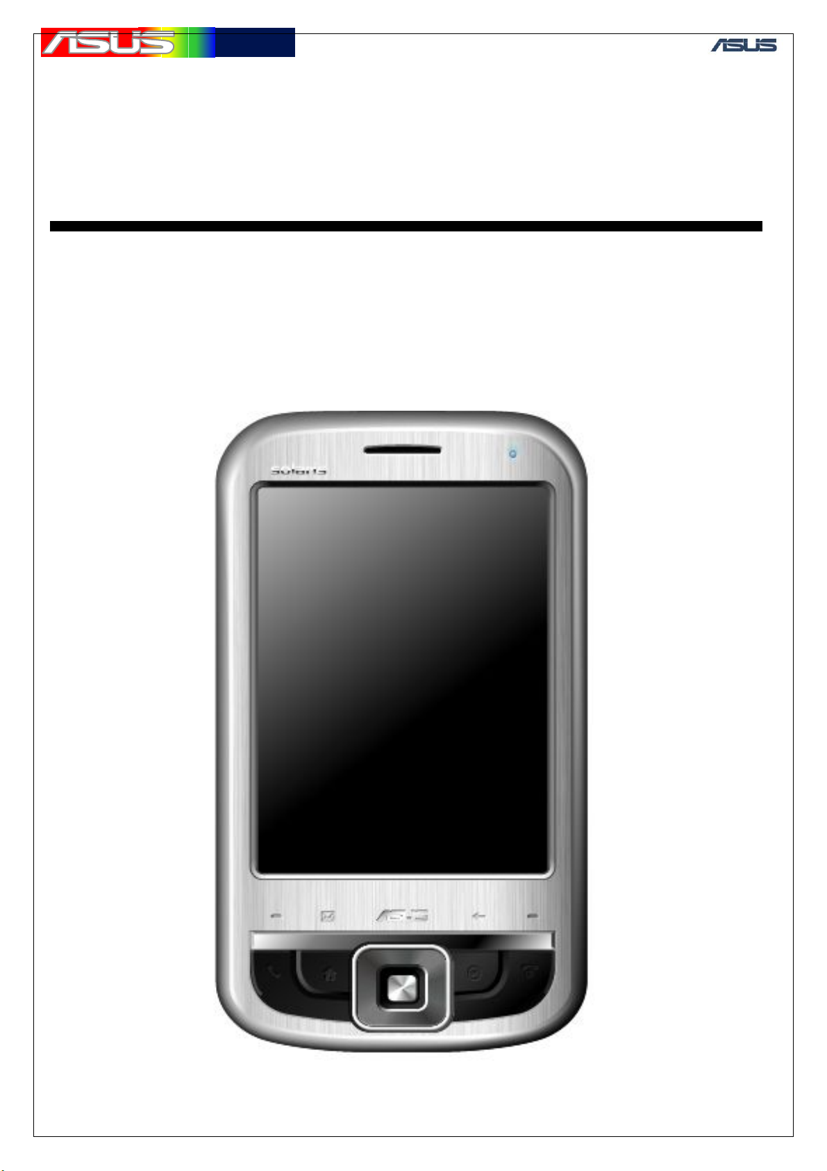
Solaris: WCDMA/GSM/GPS PDA Phone ( Mars-series)
1.1 Specification
Operation system : Windows Mobile 6.0
CPU : Marvell PXA270 520MHz
Main Memory : 256MB Flash (M-System H3) + 64MB SDRAM
(INFINEON HYB18L512320BF-7.5)
Modem : Intel PCPXA900 312MHz
Modem Memory : 32MB Stacking Flash + 16Mb PSRAM (Micron
MT45W1M16PDGA)
LCD : 3.5 inch, QVGA, Transflective, Touch-panel
(TPO TD035STED8)
Camera : 2M pixel, Fixed Focus (Walton COB20MZ1-solaris)
WiFi : IEEE 802.11b/g (ALPS UGGZ3X10BA)
Bluetooth : Bluetooth V2.0 (CSR BC41B143A05-IXB-E4)
GPS : SiRF StarIII GSC3F/LP-7979
Extended memory : Mini-SD Socket
Battery : 1530mAh (Welldone SBP-14)
ID Overview
3
Page 5
華華碩碩電電腦
腦
GTC ■ Service Manual
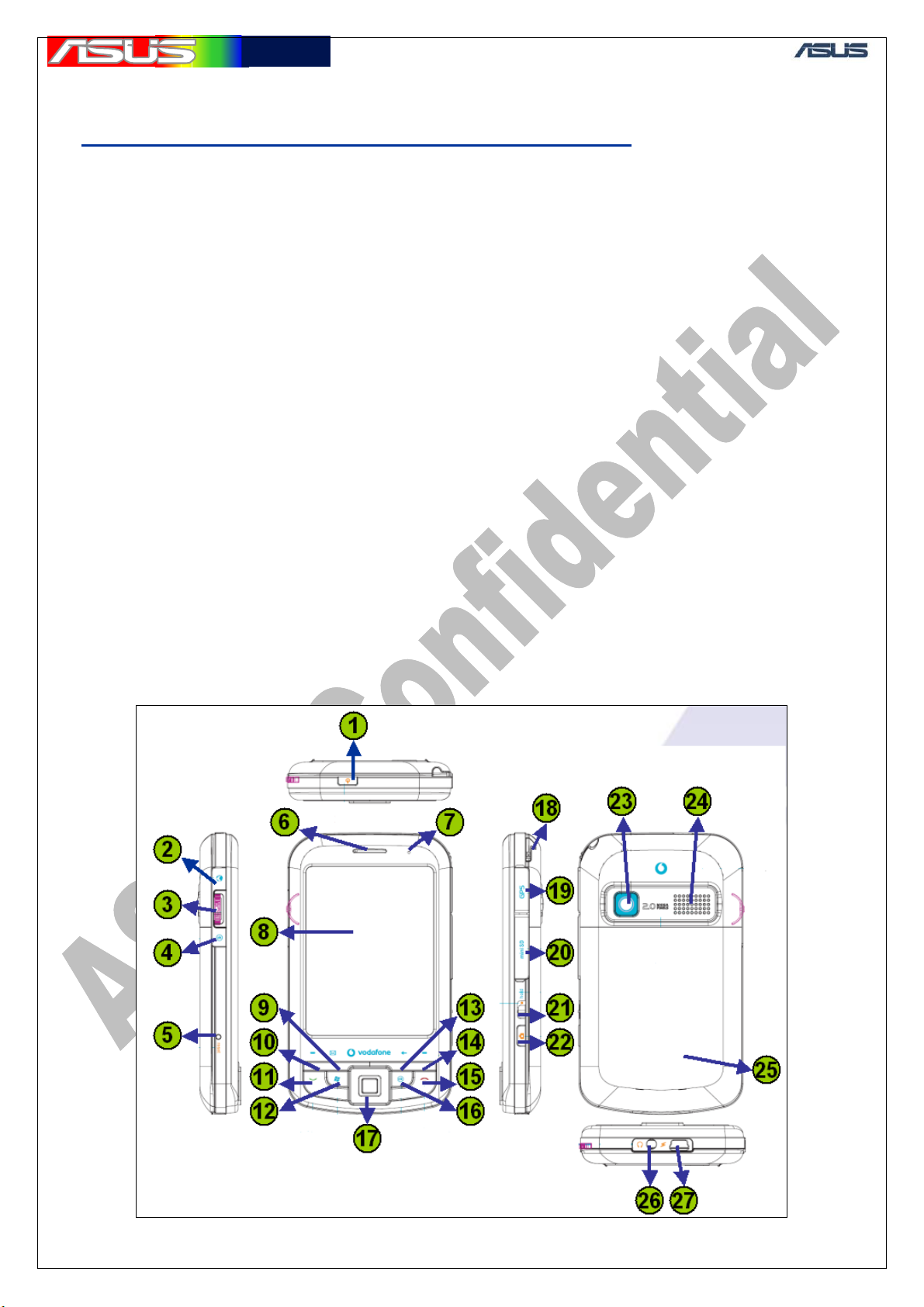
Main key function Description
1.Power Key
2.Explorer Key
3.3-way Navigation-Key
4.OK Key
5.Reset Key
6.Receiver
7.Notification LED
8.LCD (Touch)
9.Message center
10.Function Key1
11.Send Key
12.Start Key
13.Back Key
14.Function Key2
15.End Key
16.OK Key
17.5-way Navi-Key
18.Stylus
19.Active GPS antenna socket
20.Mini-SD socket
21.Hold Key
22.Camera Key
23.Camera
24.Speaker
25.Battery Cover
26.Phone Jack
27.Mini USB socket
4
Page 6
華華碩碩電電腦
腦
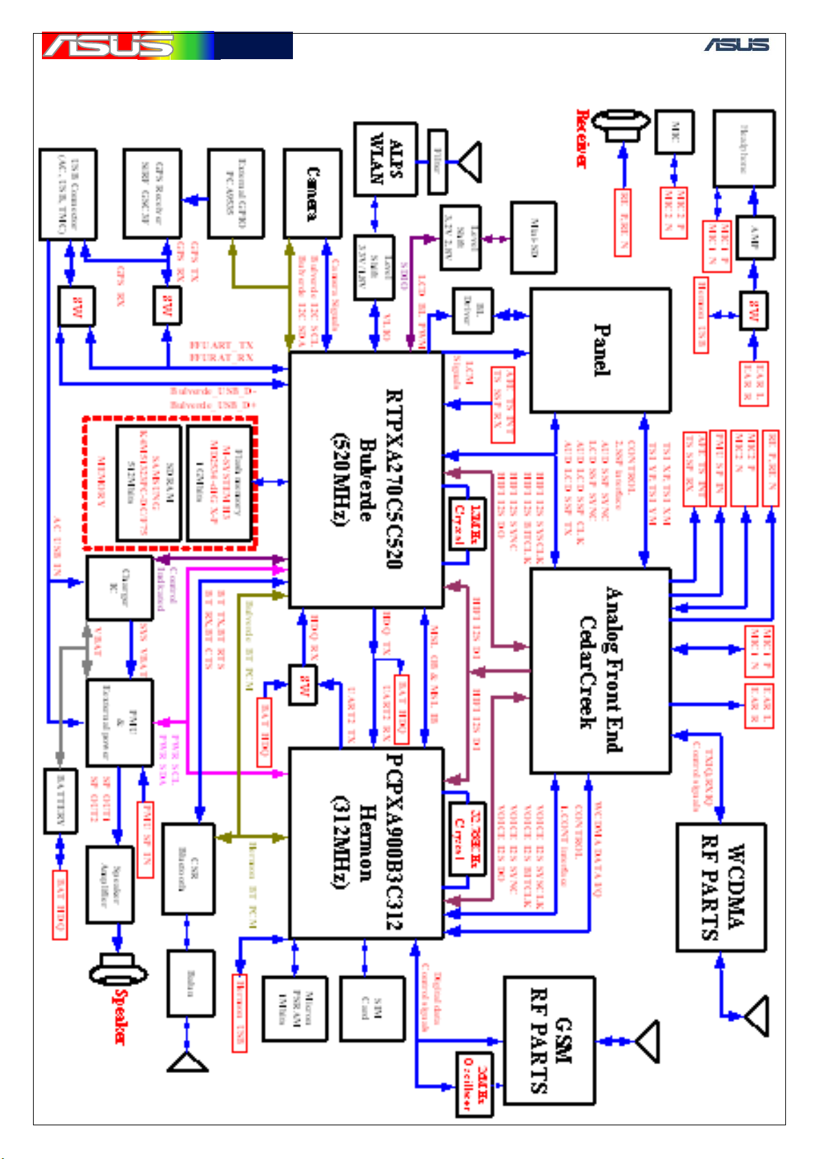
2. Block Diagram
GTC ■ Service Manual
5
Page 7
華華碩碩電電腦
腦
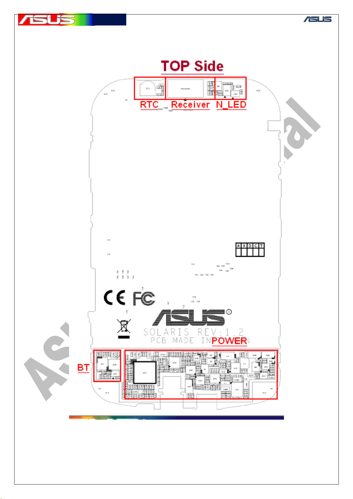
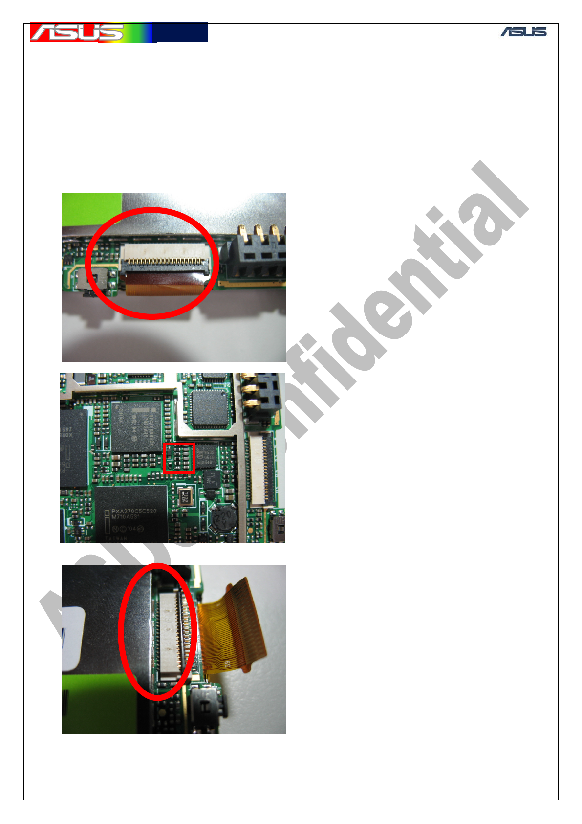
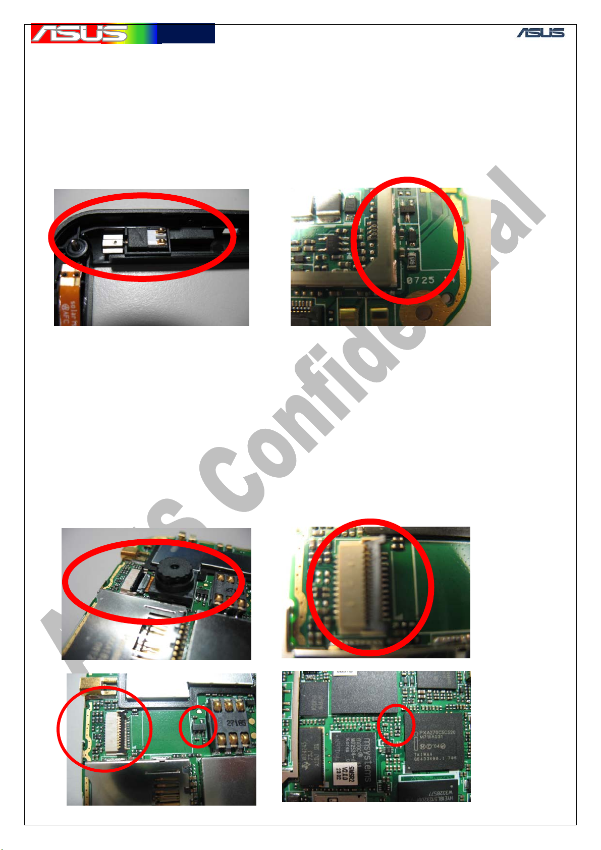
3. BASE Band Placement
3.1 Solaris TOP View
GTC ■ Service Manual
6
Page 8
華華碩碩電電腦
腦
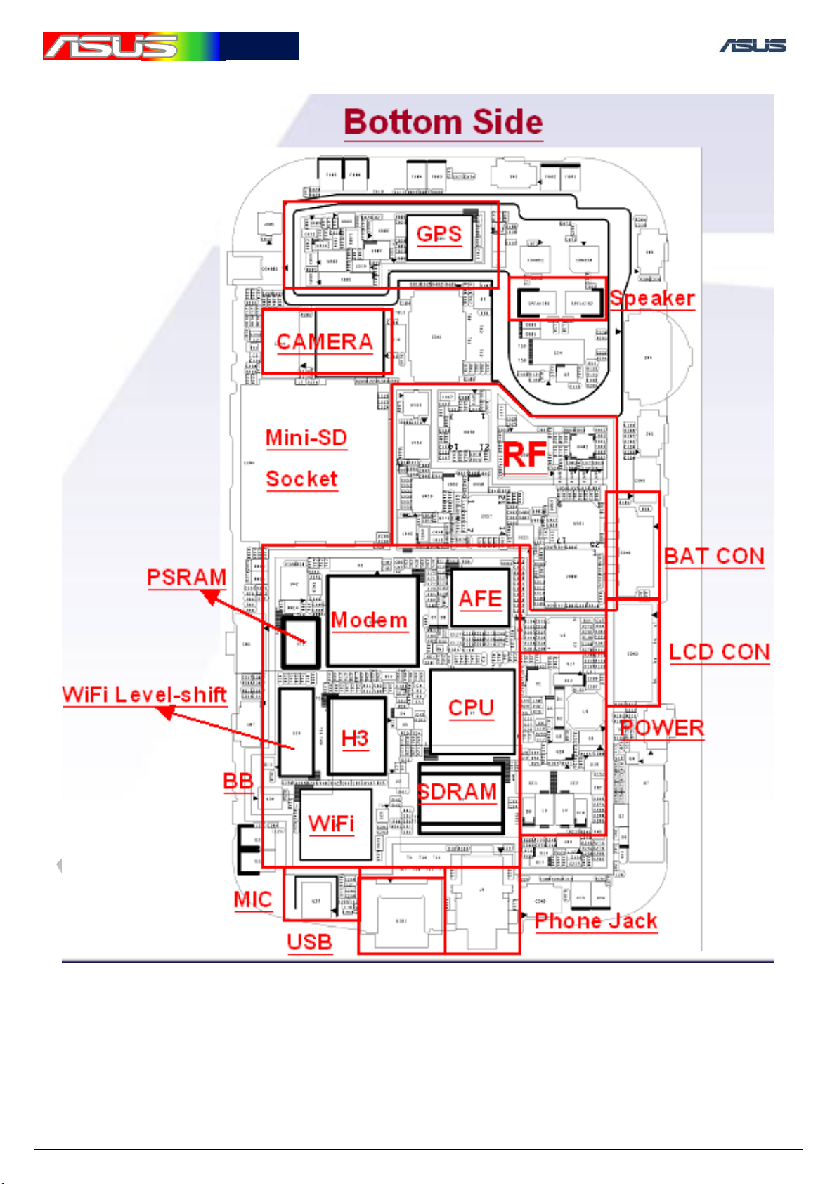
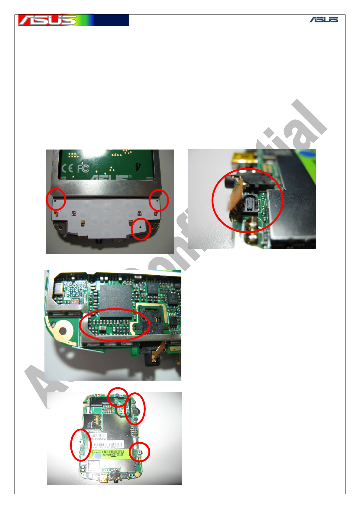
3.2 Solaris Bottom View
GTC ■ Service Manual
7
Page 9
華華碩碩電電腦
腦
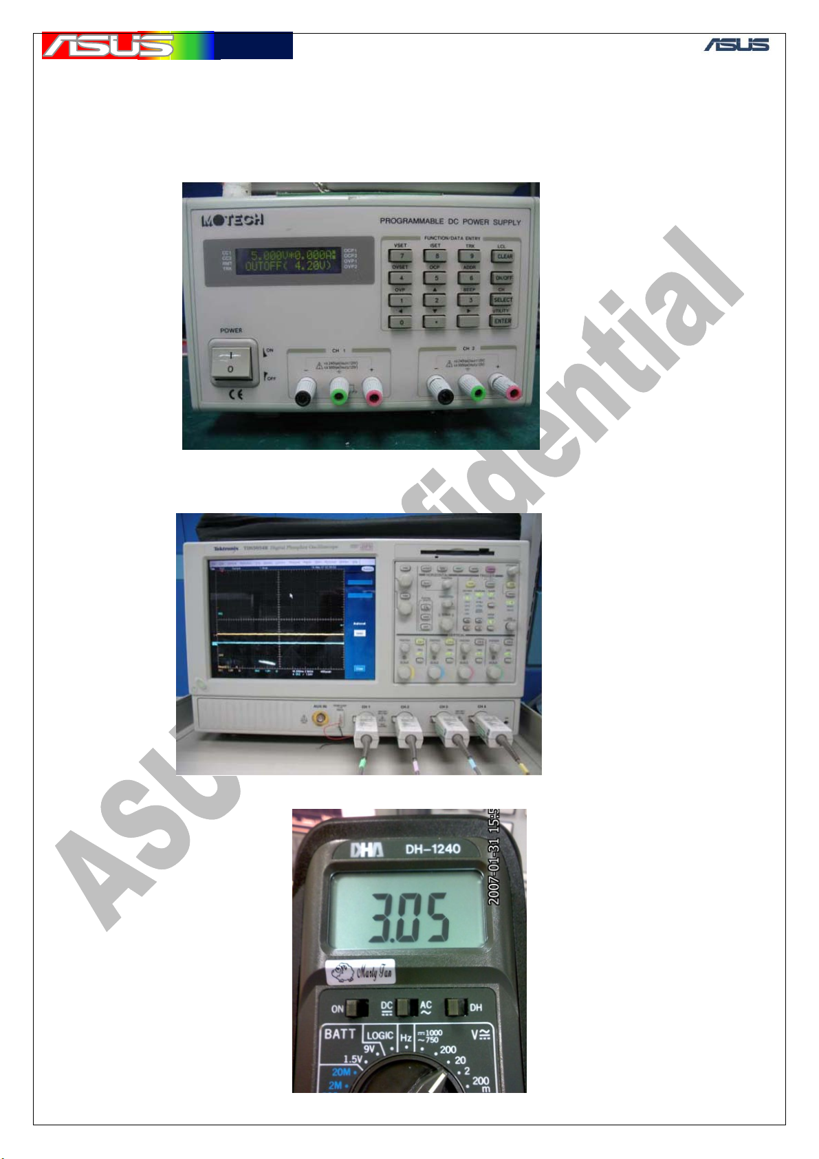
4. Base Band Repair Tooling
4.1 HW
Power source: power supply (Monitor current)
Digital Phosphor Oscilloscope
GTC ■ Service Manual
Digital Meter
8
Page 10
華華碩碩電電腦
腦
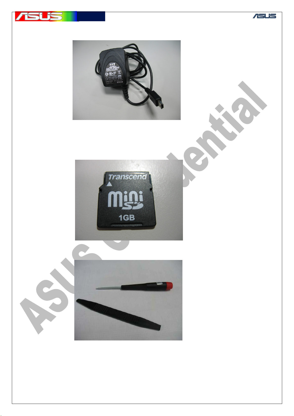
GTC ■ Service Manual
Adapter: JSP050090UU
Mini SD with test-program
ME tool
9
Page 11
華華碩碩電電腦
腦
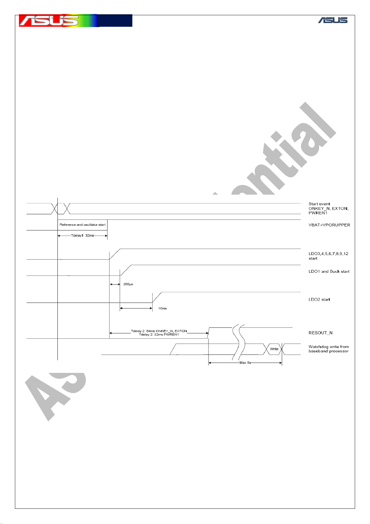
5. Chip Timing Sequence
5.1 PMU Timing Sequence
Base band start-up sequence:
1. The DA9030 powers up the following LDO for the Baseband: LDO3, LDO4,
LDO5, LDO 6, LDO8, LDO7, LDO9,LDO12, LDO14 (I/O LDOs, RF l LDOs
and VCTXO LDO).
2. After delay of 200μs from end of stage 1 the DA9030 powers up LDO1 and
DC/DC1 (Base band core and PLL).
3. After delay of 10ms from end of stage 2 the DA9030 will power up LDO2
(internal Flash LDO).
4. After delay of Tdelay2 (32ms) from the start of the start-up sequences (stage 1)
the DA9030 will raise RESOUT_N
signal to the base-band chip
GTC ■ Service Manual
.
10
Page 12
華華碩碩電電腦
腦
GTC ■ Service Manual
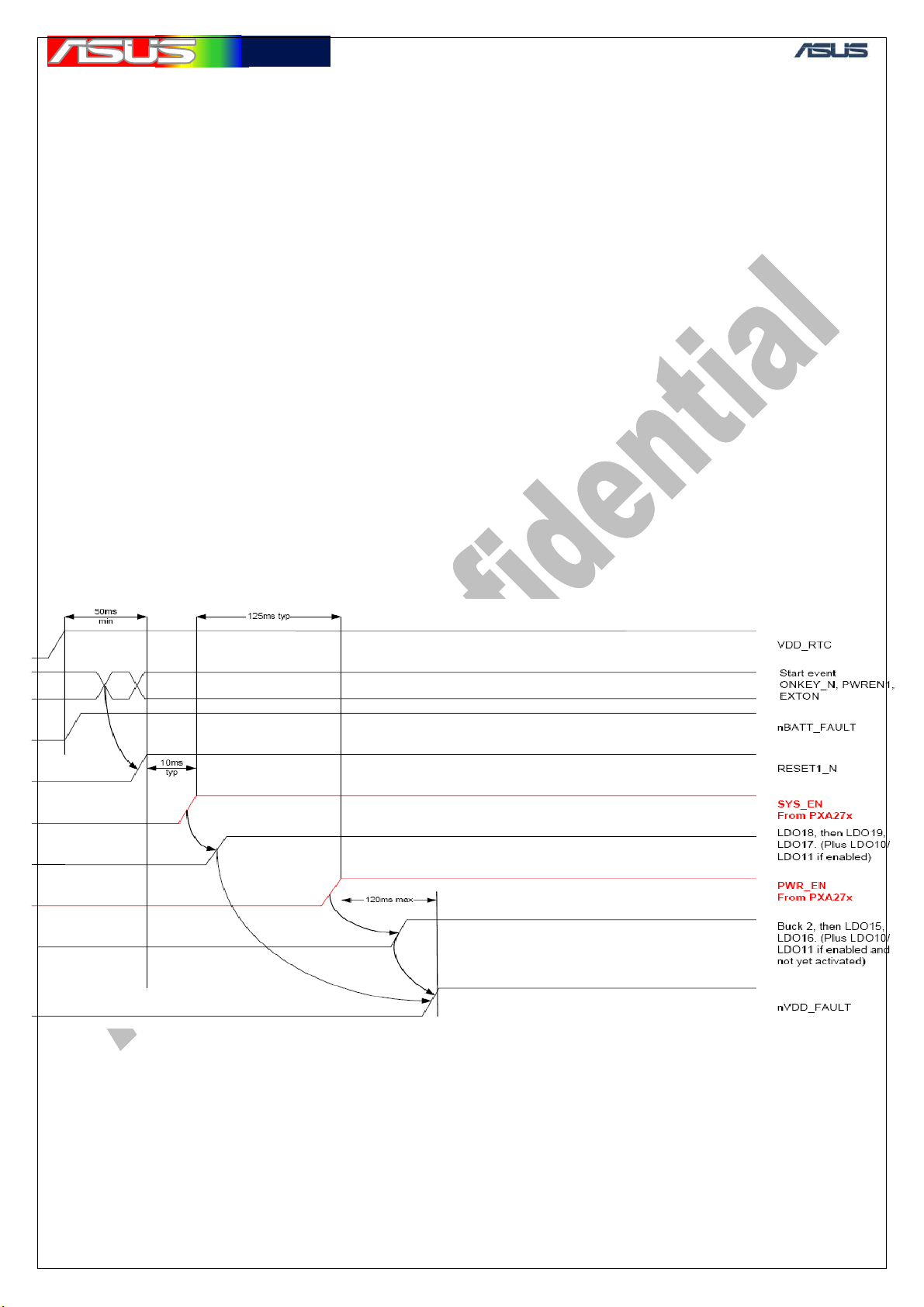
5.2 CPU Timing sequence
PXA27x Start-up sequence:
1. Once the VBAT has risen above the VBATUNDER threshold, the DA9030
de-asserts (High) BATT_FAULT signal to
the PXA27x chip (indicating that VBAT is ok).
2. On receiving a start event the DA9030 de-asserts RESOUT1_N (high) (a
minimum 50ms from power up of the RTC
LDO is required to reset the PMU unit in the PXA27x and before RESOUT1_N
can be de-asserted).
3. The DA9030 waits for the PXA27x to assert (High) SYS_EN and powers up
the LDOs associated with this signal
(described below).
4. The DA9030 waits for the PXA27x to assert PWR_EN (typically 125ms after
asserting SYS_EN) and powers up the
sources associated with this signal (described below).
5. After all sources are stable for the PXA27x, the DA9030 will de-assert (High)
VCC_FAULT (so the PXA27x can
continue with its power up sequence).
11
Page 13
華華碩碩電電腦
腦
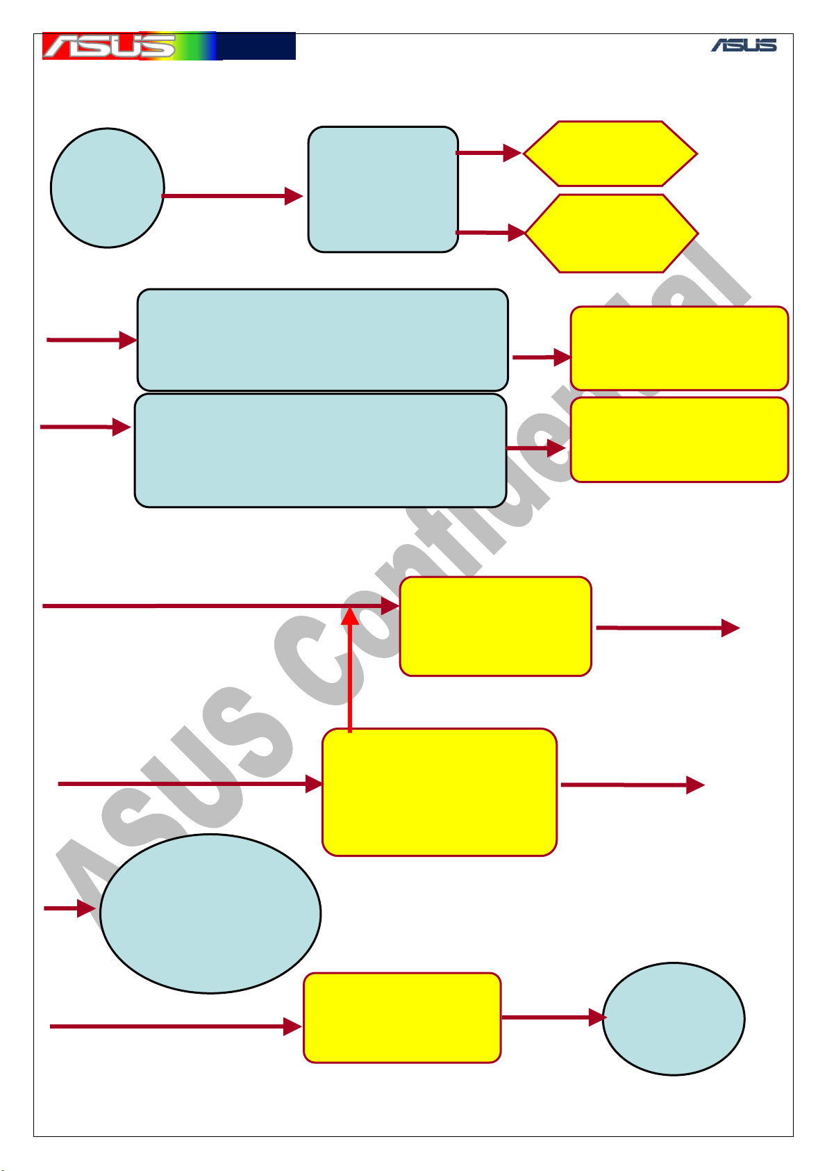
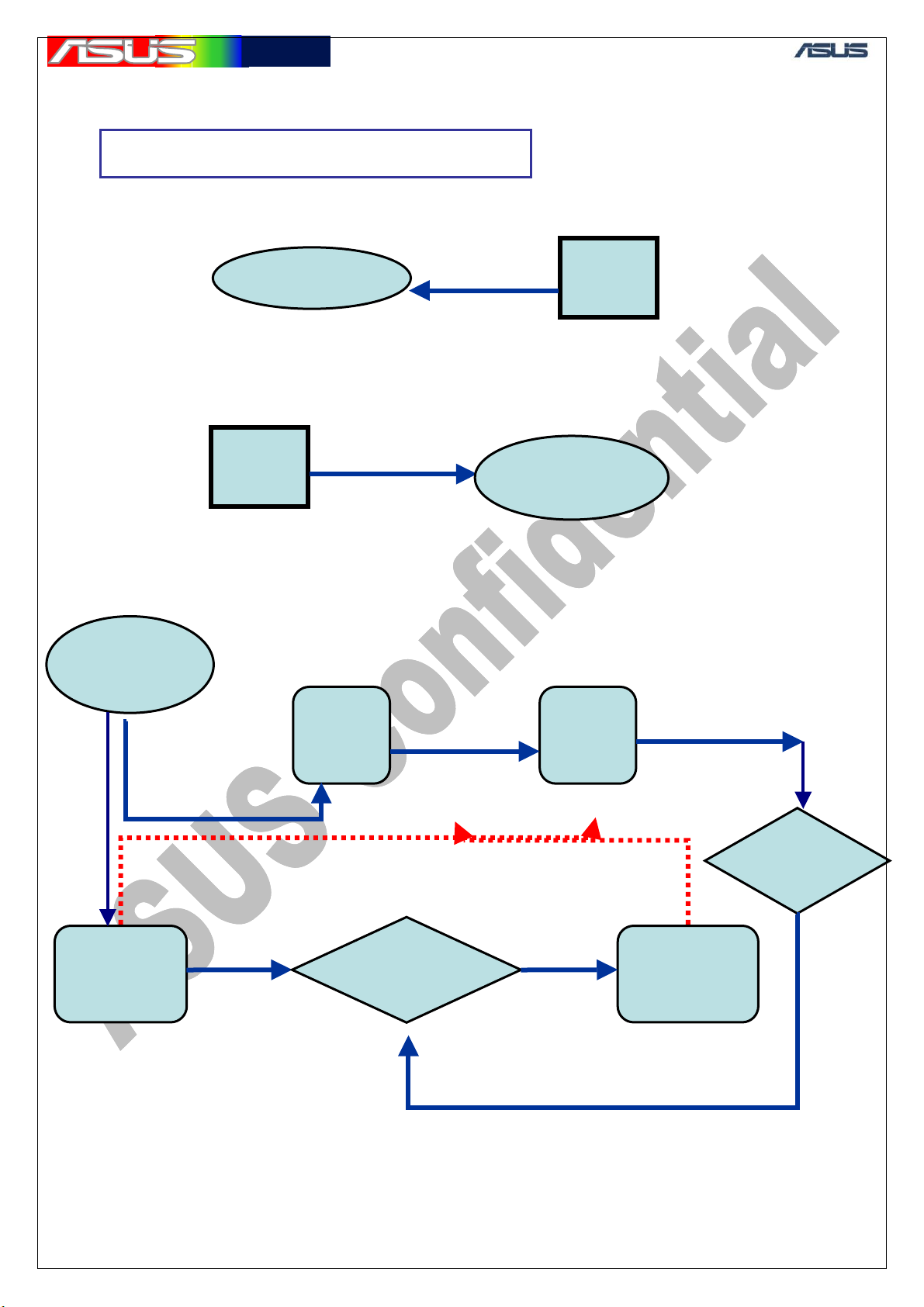
5.3 System Flowchart
GTC ■ Service Manual
Plug-in
Battery
(VBAT)
PWR_ON#
=VBAT
VLDO_RTC =
2.65V
Hermon_XTAL_IN(OUT) = 32KHz
VCXO_CLK(BB_CLK = 13MHz
Hermon_RESET_IN# = 2.65V
PMU_RESOUT_HERMON_OD#= 2.8V
32K_OUT_SLP = 32KHz
Bulverde_PXTAL_IN(OUT) = 13MHz
Bulverde_HW_RST# = 2.8V
Bulverde_SW_RST# = 2.8V
Push
Power-Key
PMIC with
Hermon
Power On
PMIC with
Bulverde
Hermon
Execute Boot-code
from Stack-Flash
Bulverde
Execute Boot-code
from Flash (U9)
Read
ON-mode
Check power-on
mode
Normal, download,
charging
Hermon
Execute OS in
RAM (U11)
from Stack-Flash
Re-boot
Write mode to
PMIC
Reset Hermon
Bulverde
Execute OS in RAM (U8)
from Flash (U9)
Read
ON-mode
Bulverde_SD_CS
0#
Bulverde_NF_
CS#
Bulverde
Init pheripherals
(Phone, LCD...)
12
Windows
START
Page 14
華華碩碩電電腦
腦
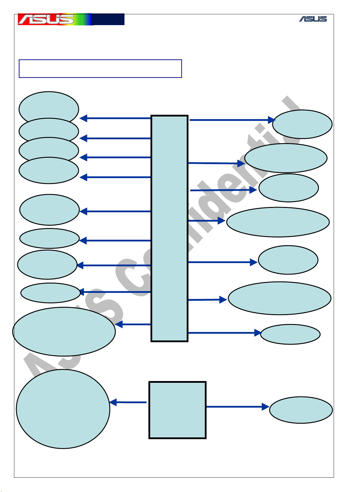
5.4 Power supply Block
¾ Power system ~ Supplied
CPU
VCORE
CPU RTC
Mini-SD
LCD
Mic,
Headphon
CPU PLL
CPU
SRAM
CPU USB
CPU IO(2.8V), Flash
CORE
PCA9535,
Modem IO(1.8V)
Modem memory,
Codec VCCP
CPU IO(1.8V),
Flash IO
SDRAM, Camera
VLDO15, 1.3V
VLDO16, 1.1V
VLDO17, 3.2V
VLDO18, 2.8V
VCORE_2, 1V~1.5V
VLDO3, 2.8V
VLDO10, 3.2V
VLDO11, 2.8V
VLDO13, 2.1V
AUX_1V8, 1.8V
PMU
U14
DC/DC
(U15)
GTC ■ Service Manual
VCORE_1, 1.25V
VLDO_RTC, 2.65V
VLDO1, 1.2V
VLDO3, 2.8V
VLDO5, 2.8V
VLDO6, 1.8V ~ 3V
VLDO19, 1.8V
Modem
VCORE
Modem RTC,
GPS RTC
Modem
PLL
Modem IO(2.8V),
Codec VCC
Codec
VCCA
Modem SIM, SIM
card
BT CORE
13
Page 15
華華碩碩電電腦
腦
(
GTC ■ Service Manual
5.5 Power system Supplied Block
¾ Power system ~ Supplied
Camera 2.8V
DC/D
LCD LED,
20V(Max)
CAM_2V8, 2.8V
C
LDO
U18
LCD
Backlight
5.6 Power System Charging block
Charger IC
(U21)
Cable
insert
AC_USB_IN, 5V
CHG_ST1, CHG_ST2
Charging
USB,
100mA
PMIC
(U14)
PMU_IRQ#, 0V
Change
charging
CPU
(U1)
Charging
CHG_P_SEL, CHG_USB_ISET, CHG_DIS
USB_C_D+, 3.2V
Detect
type
Battery
(CON2)
14
Page 16
華華碩碩電電腦
腦
r
6. Trouble shooting
6.1 General Process
¾ Trouble shooting ~ Procedure
Check orientation, position
Check SMT
components
PCBA
Abnormal
Set Power supply to 4V,
and
limit current to 1A
Press Power Key
(>5sec)
Monitor
current
RUN
Test-prog
GTC ■ Service Manual
Connect +,- to VBAT, GND
Check connector, components
System
Abnormal
Failed item in System level Failed item in Board level
Disassemble
assembly parts
15
Page 17
華華碩碩電電腦
腦
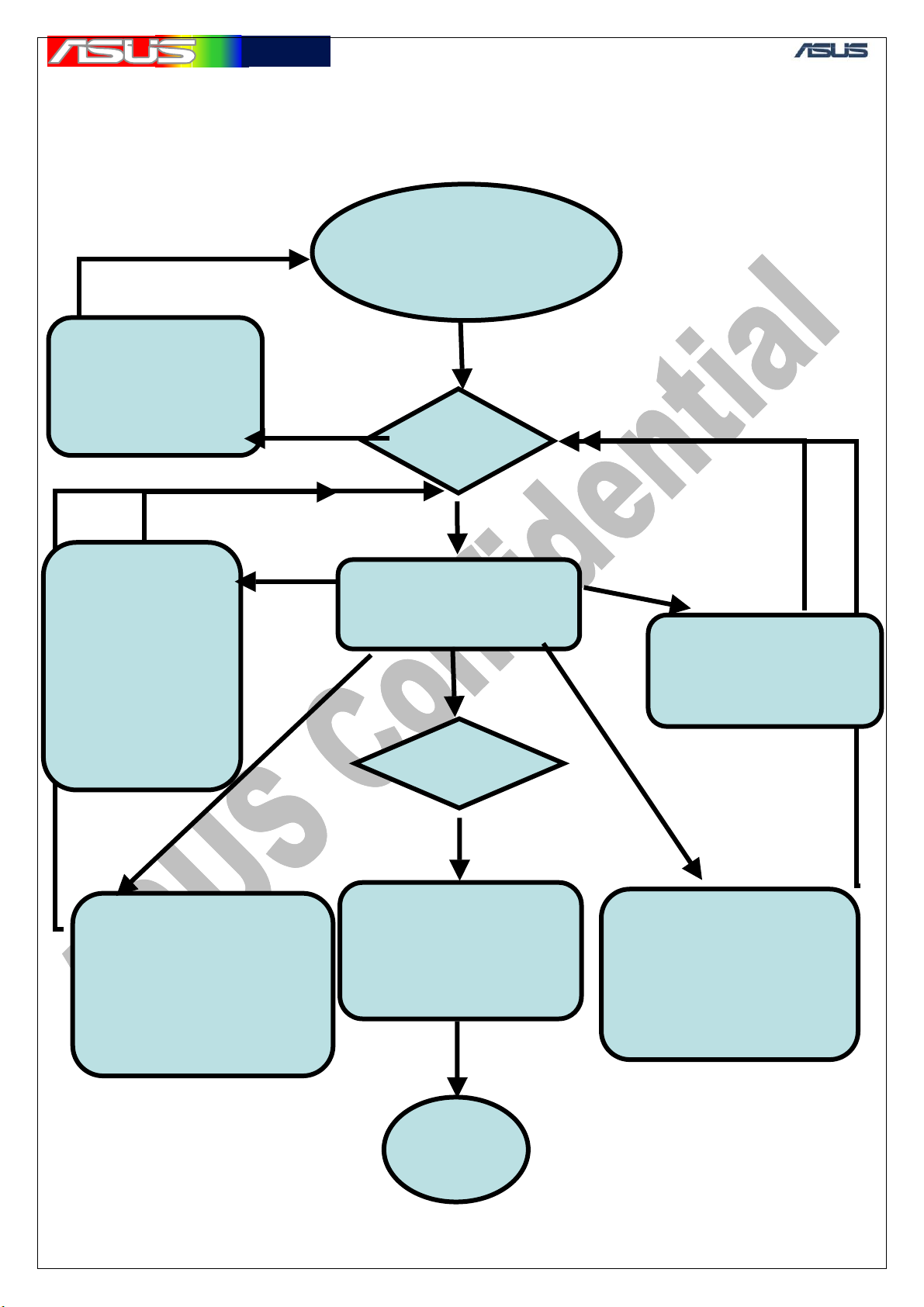
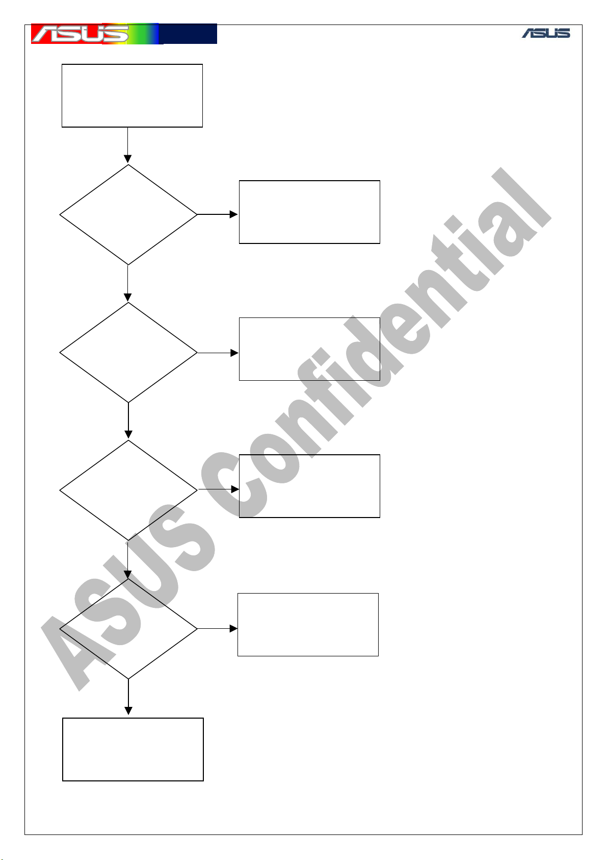
6.2 Can’t Power ON process
VBAT & GND short
U14, U15, U17, U18,
1. CPU failed to
load image
2. Flash failed to
provide image
3. SDRAM failed
to execute image
see note_1
Complete rework
Check supplied
components
LED1, U21
Complete rework
PMIC provide
abnormal power
(U14)
Check power supplied
domain
see note_2
Abnormal
Limit current
Abnormal
200mA -> 0mA
(8sec)
Abnormal
Suddenly
0mA
Check LCD connector
Set Power supply to
4V, and
limit current to 1A
Connect +,- to VBAT, GND
Monitor
current
Current ~ 0mA
Press Power Key
(>5sec)
Abnormal display
Monitor
Complete rework
Normal
200~400mA
and components
between
LCD and CPU
END
GTC ■ Service Manual
Complete rework
Abnormal
> 400mA
Check components
Abnormal
Sustain
U14 is the most case.
orientation and
touch BGA chip, feel
temperature.
0mA
Check Battery
connector and
VBAT-related
components
16
Page 18

華華碩碩電電腦
腦
GTC ■ Service Manual
Note 1
Measure reset signal (Bulverde_HW_RST#, Bulverde_SW_RST#), High =>
Inspect related components.
2. Measure clock signal (Bulverde_PXTAL_IN, Bulverde_PXTAL_OUT),
13MHz. (Bulverde_32K_IN), 32KHz.
Inspect U1, X1. And U10.
3. Measure chip-select signal (Bulverde_NF_CS#), H-L...
(Bulverde_SD_CS0#), H-L... => Inspect U1
4. Measure data-signal (D0), H-L... => Inspect U8, U95. Un-mount Flash(U9)
and re-download image. And then re-mount.
Note 2
1. Don’t supply VBAT to PCB, and measure impedance of all power supplier
(VCORE_1, VCORE_2.....)
Note3
Re-download image
2. If re-download image remain failed, please un-mount Hermon (U10) and
re-download by DATA-IO.
17
Page 19
華華碩碩電電腦
腦
7. Trouble shooting
7.1 Touch panel failed
1. Check LCD connector (CON3) => Assembly, Soldering issue
2. Replace LCD to golden sample => Component issue
3. Check communicated components between LCD (CON3) and Codec (U13)
=> Soldering issue
GTC ■ Service Manual
18
Page 20
華華碩碩電電腦
腦
GTC ■ Service Manual
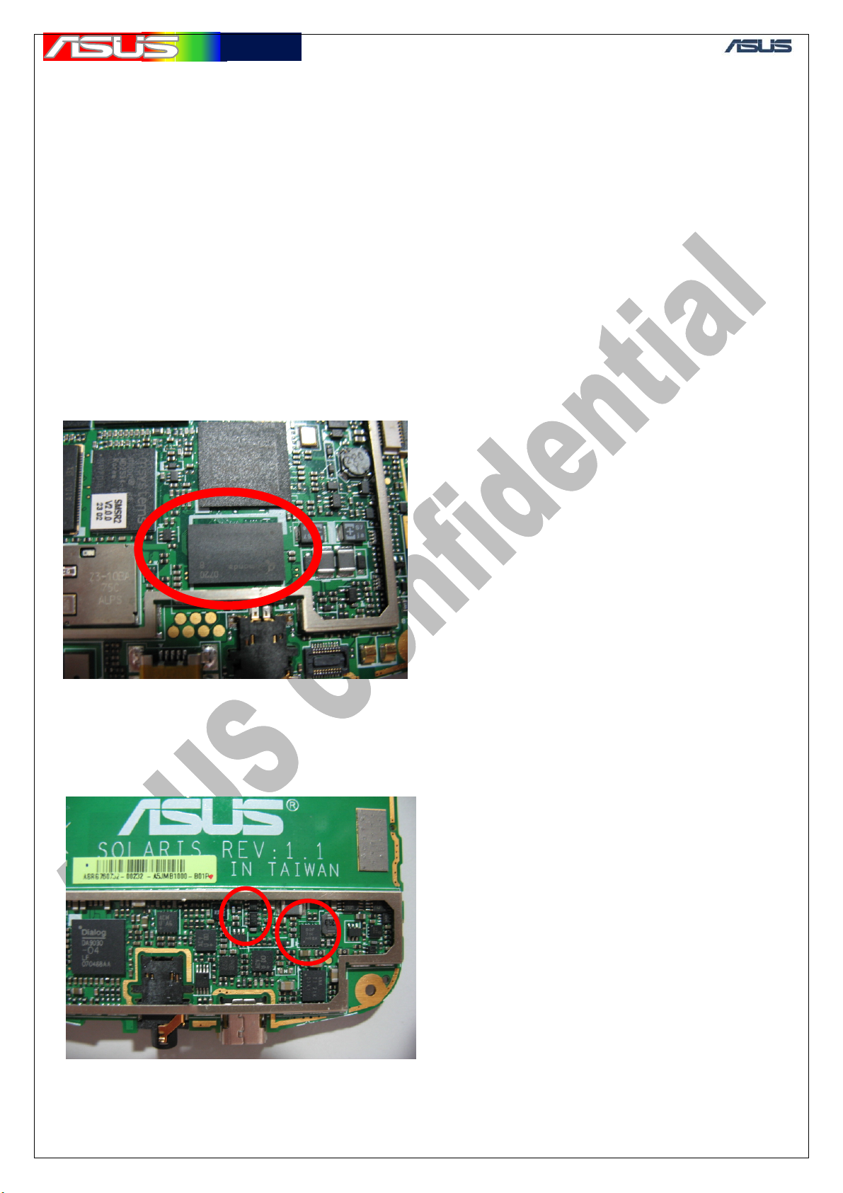
7.2 SDRAM
1. Check SDRAM (U8) and peripherals => Soldering issue
2. Measure power supplied, AUX_1V8_2 (R43) => Power supplied issue, check
U15, Q5 peripherals
3. Measure clock signal, Bulverde_SDCLK1 (R1) => Check U1 and peripherals
4. Measure chip-select signal, Bulverde_SD_CS0# (T51) => Check U1 and
peripherals
Note: If normal display and hang-up,
Modem failed to load image.
see note_3
END
BAT_HDQ
19
Page 21
華華碩碩電電腦
腦
GTC ■ Service Manual
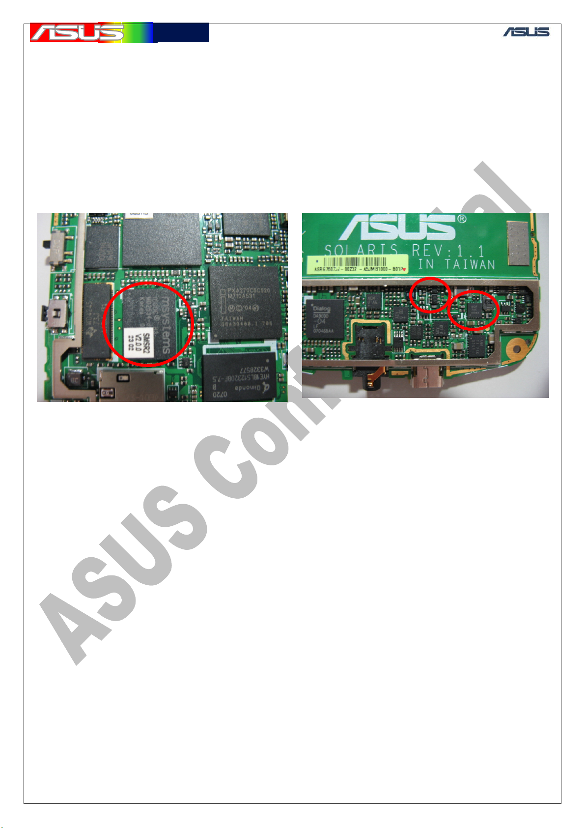
7.3 Flash failed
1. Check Flash (U9) and peripherals => Soldering issue
2. Measure power supplied, AUX_1V8_2 (R43), VLDO18 (R49) => Power
supplied issue, check U15, Q5 peripherals
3. Measure chip-select signal, Bulverde_NF_CS# (T49) => Check U1 and
peripherals
4. Measure chip-select signal, M-SYSTEM_BUSY# (R47) => Components
issue, replace U9
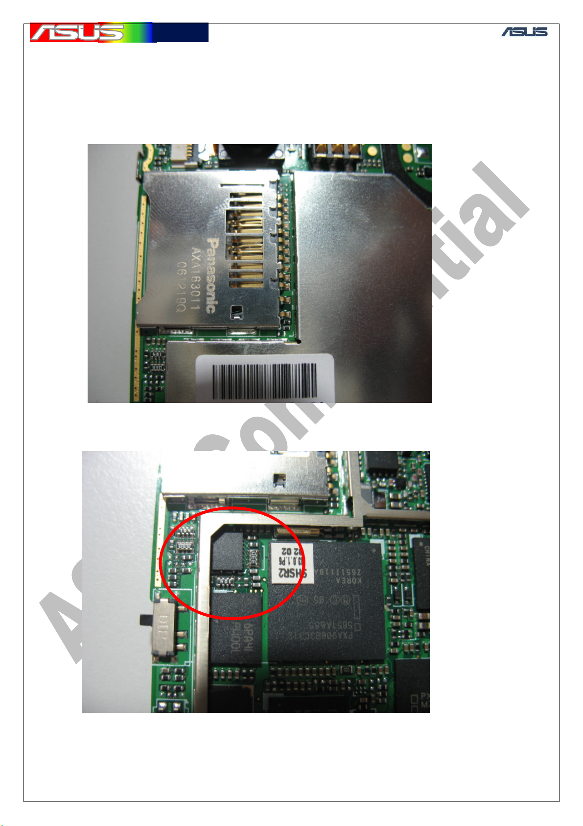
7.4 SDCARD
1. Check mini-SD socket (CON6) => Soldering issue
2. Check communicated components between mini-SD (CON6) and CPU (U1),
U42 and peripherals => Soldering
3. Measure power supplied, VLDO10 (R290) => Power supplied issue, Check
PMIC (U14)
4. Measure clock signal, SDMMC_CLK (R5) => Check U1 and peripherals
1. Check SDRAM (U8) and peripherals => Soldering issue
2. Measure power supplied, AUX_1V8_2 (R43) => Power supplied issue, check
U15, Q5 peripherals
3. Measure clock signal, Bulverde_SDCLK1 (R1) => Check U1 and peripherals
4. Measure chip-select signal, Bulverde_SD_CS0# (T51) => Check U1 and
peripherals
Note: If normal display and hang-up,
Modem failed to load image.
see note_3
END
BAT_HDQ
20
Page 22
華華碩碩電電腦
腦
21
GTC ■ Service Manual
Page 23
華華碩碩電電腦
腦
GTC ■ Service Manual
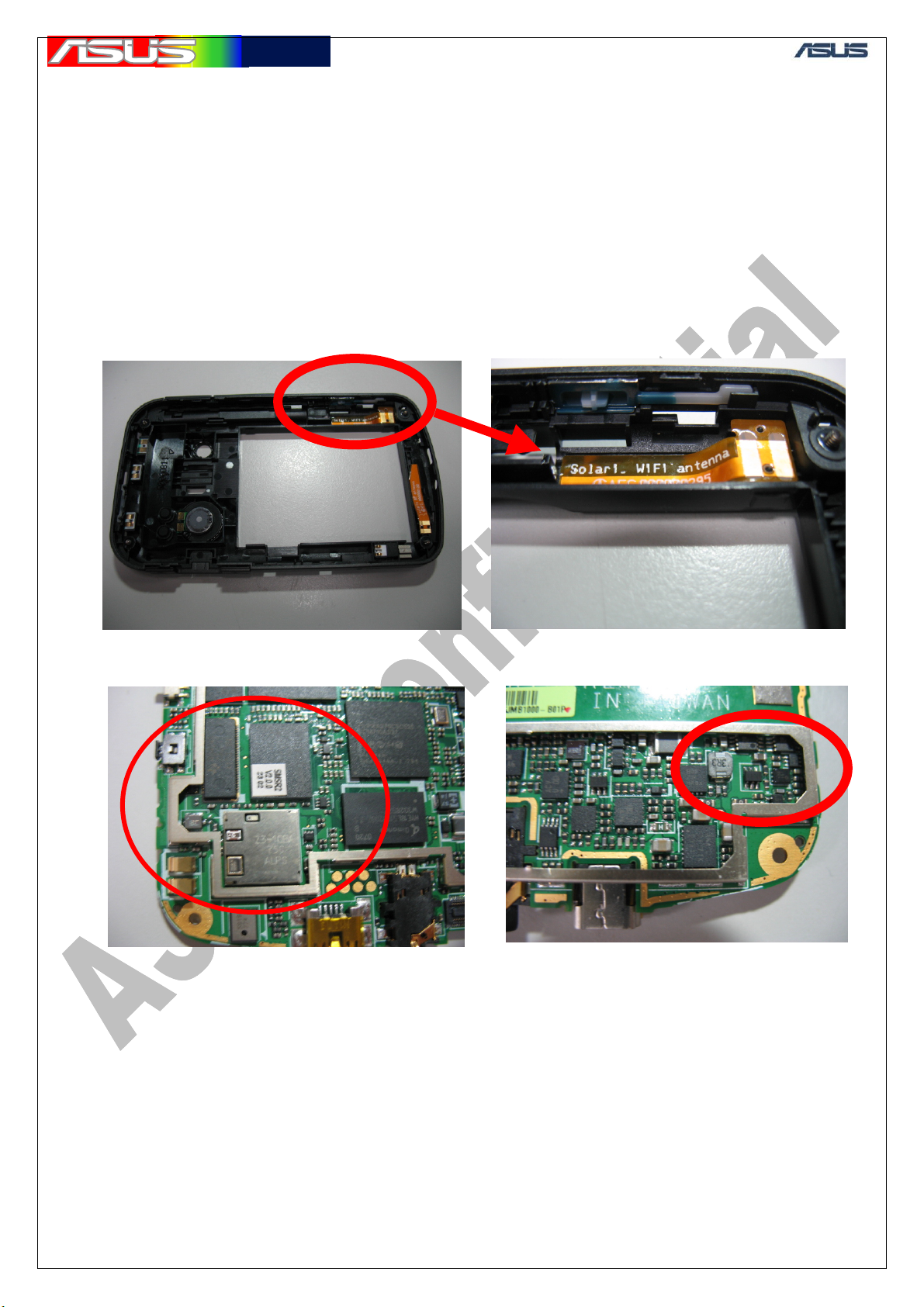
7.5 WiFi failed
1. If performance failed, check assembly WiFi antenna, Spring (U31,U32)
contact => Assembly, Soldering issue
2. Check WiFi (U35), Level-shift (U36) and peripherals => Soldering issue
3. Measure power supplied, WLAN_3V3 (R277), WLAN_1V5 (R278) => Q12,
U41 and peripherals, soldering issue
4. Measure chip-select, Bulverde_WLAN_CS# (R255) => Components issue,
U35, U36, U1 and peripherals
22
Page 24
華華碩碩電電腦
腦
GTC ■ Service Manual
7.6 Modem-BUS failed
1. Check Modem (U10), PSRAM (U11) and peripherals => Soldering issue
2. Clean-boot or Re-download image => Image crash
3. Measure power supplied, VCORE_1 (R79) and etc. => Check PMIC (U14)
and peripherals
4. Measure clock signal, VCXO_CLK ( OSC1), 13MHz. X’TAL (X2), 32KHz.
=> Check PMIC (U14) and peripherals
23
Page 25
華華碩碩電電腦
腦
GTC ■ Service Manual
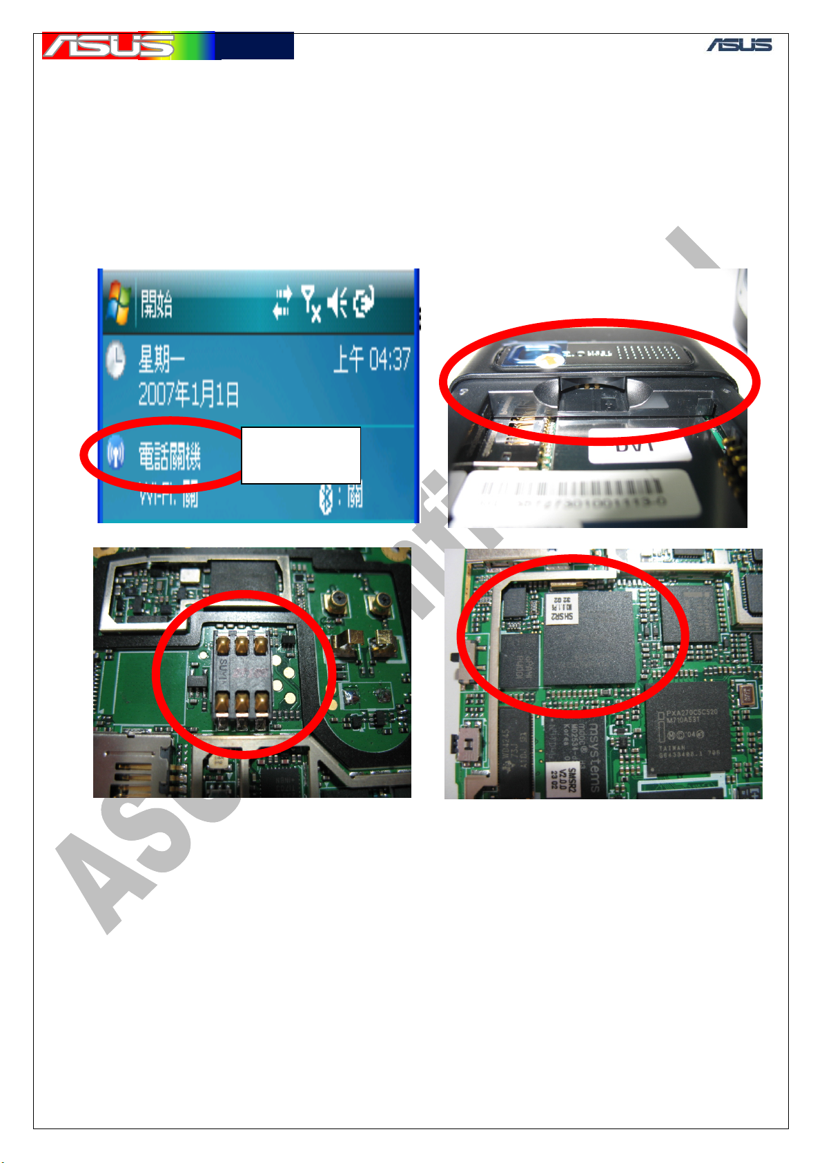
7.7 SIM failed
1. Check Wireless-manager, Phone must be ON => Operation issue
2. Check antenna cover => Assembly issue
3. Check SIM socket (CON1) and peripherals => Soldering issue
4. Check Modem (U10) and peripherals => Soldering issue
Phone OFF
7.8 LED
1-1. If Keypad LED failed, please check Keypad FPC assembly => Assembly
issue
1-2. If assembly is fine, please check connector (CON5) and peripherals =>
Soldering issue
2-1. If notification LED (LED1) failed, check LED1 and peripherals =>
Soldering issue
24
Page 26
華華碩碩電電腦
腦
GTC ■ Service Manual
7.9 Display failed
1. Check LCD connector (CON3) => Assembly, Soldering issue
2. Replace LCD to golden sample => Component issue
3. Check power supplied (R216), reset# (R198), SD (R270) => Soldering issue
4. Check communicated components between LCD (CON3) and CPU (U1) =>
Soldering issue
25
Page 27
華華碩碩電電腦
腦
GTC ■ Service Manual
7.10 Battery failed
1. Double check Battery on fine device => Component issue
2. Check Battery connect (CON2) => Soldering issue
3. Check signal, BAT HDQ(CON2, pin4), Q8, U20 => Soldering issue
26
Page 28
華華碩碩電電腦
腦
GTC ■ Service Manual
7.11 Vibrator failed
1. Check Vibrator => Assembly issue
2. Replace Vibrator to golden sample => Component issue
3. Check power supplied (R36), Driving signal (Q2) => Soldering issue
7.12 Camera
1. Check Assembly => Assembly issue
2. Replace Camera module to golden sample => Component issue
3. Check Camera connector => Soldering issue
4. Check power supplied (U18), CAM_RESET# (R187), CAM_STBY (R185),
Bulverde_I2C (RN1), CAM_MCLK (R8)
26MHz => Soldering issue
5. Check signal from Camera, CAM_XXX => Component issue
27
Page 29
華華碩碩電電腦
腦
GTC ■ Service Manual
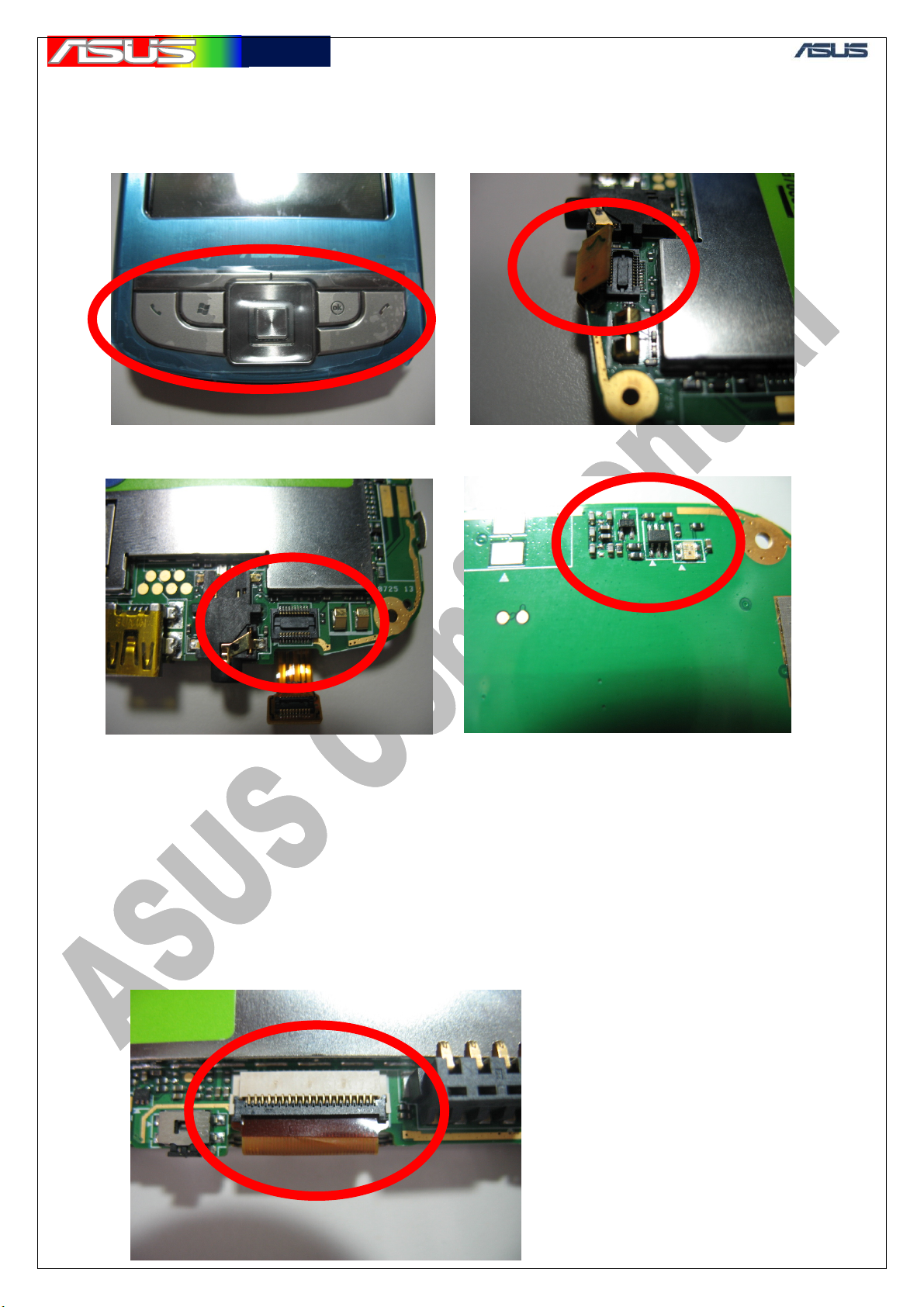
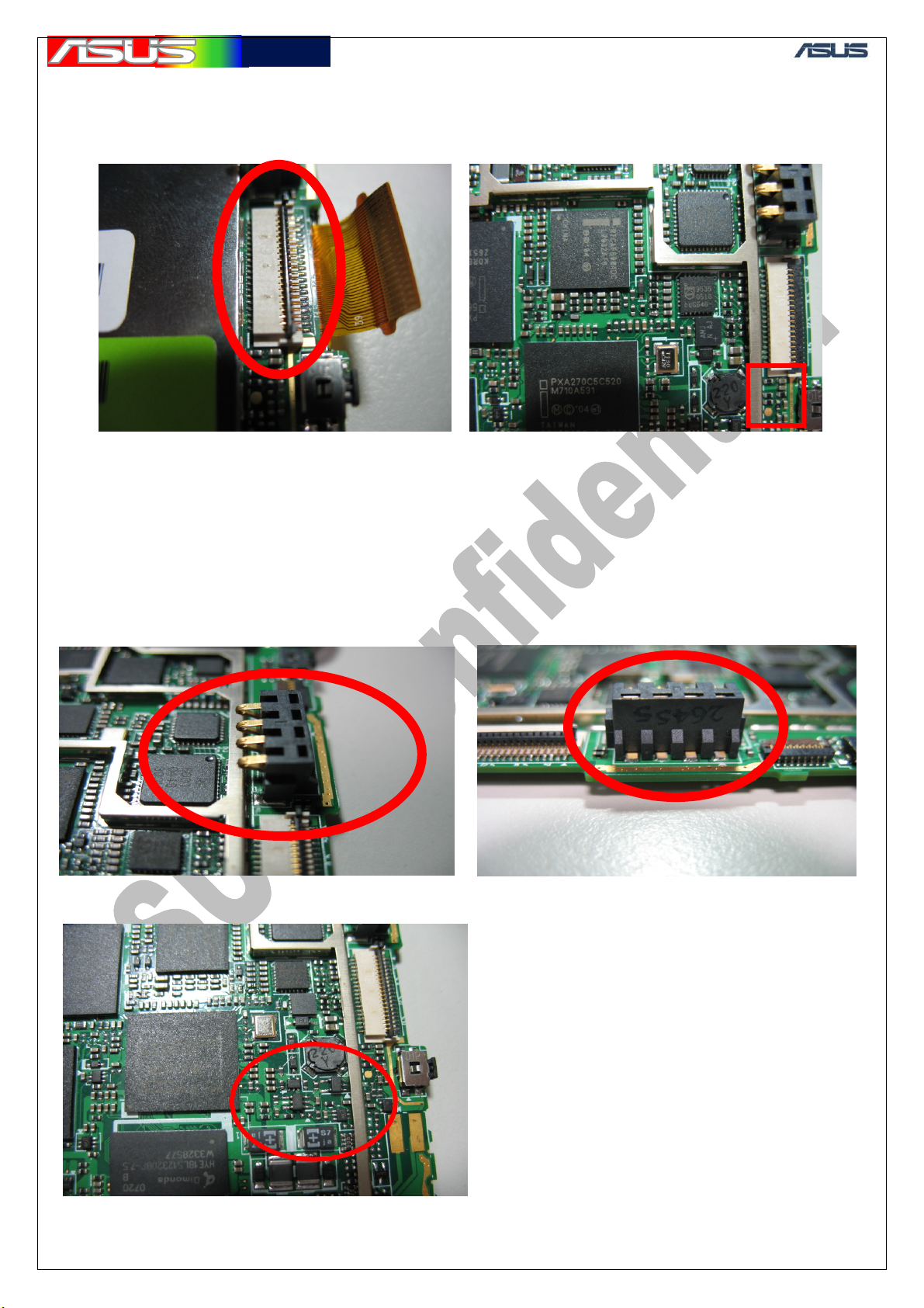
7.13 Button failed
1. Check stick position of keypad board => Assembly issue
2. Check assembly between keypad and connector (CON5) => Assembly issue
3. Replace to golden sample => Component issue
4. Check signal KP_XXX => Soldering issue
5. Check assembly of side-Key => Assembly issue
6. Check SMT switch (SW1 ~ SW7) => Soldering issue
28
Page 30

華華碩碩電電腦
腦
GTC ■ Service Manual
7.14 BT failed
1. If performance failed, check assembly BT antenna, Spring (U33,U34) contact
=> Assembly, Soldering issue
2. Check BT (U38), Filter (U37) and peripherals => Soldering issue
3. Measure power supplied (R251, R252), BT_RESET# (R280), X’TAL (X3) =>
Soldering issue
7.15 Audio failed
Speaker no sound
1. Check Speaker and Spring (Speaker2, Speaker3) => Assembly, SMT issue
2. Replace to golden sample => Component issue
3. Check amplifier (U24), PMIC(U14) and peripherals => SMT issue
29
Page 31

華華碩碩電電腦
腦
GTC ■ Service Manual
Receiver no sound
1. Check Receiver and Contact-pad (Speaker1) => Assembly issue
2. Replace to golden sample => Component issue
3. Check Signal RE_N, RE_P, and Codec (U13) => SMT issue
30
Page 32

華華碩碩電電腦
腦
GTC ■ Service Manual
Headphone no sound
1. Check Phone-jack (J1) => SMT issue
2. Check switch (U26), amplifier (U29), Codec (U13) and peripherals => SMT
issue
31
Page 33

華華碩碩電電腦
腦
GTC ■ Service Manual
Headphone MIC no record
1. If headphone no sound, please repair headphone first
2. Check power supplied (R224), amplifier (U28), Codec (U13) and peripherals
=> SMT issue
Board mic no record
1. Check assembly rubber => Assembly issue
2. Check SMT mic (U27), Codec (U13) and peripherals => SMT issue
32
Page 34

華華碩碩電電腦
腦
GTC ■ Service Manual
7.16 Standby current failed
1. Manual phone-off and press power-key to entry suspend-mode => Test
program issue
2. Remove camera module => Component issue
3. Measure signal PWR_EN (T64), Low. VCXO_CLK (C86), Low => SMT
issue
33
Page 35

華華碩碩電電腦
腦
8. RF Repair Requirement
8.1 SW:
IFL software
GSM and WCDMA debug tool
Hermon image database files
8.2 HW:
Specific fixture for repair and test, following must be included
i. Hermon USB Contact and USB Cable
ii. Power Supply Contact
iii. RF Connector and RF cable (30cm)
iv. High Frequency Probe with DC Block
GTC ■ Service Manual
8.3 Equipment:
1. PC
2. Spectrum Analyzer (up to 3.0 GHz)
3. Signal Generator (up to 3.0GHz)
4. Communication tester: Agilent 8960, CMU200 or Anritsu 8820
5. Digital Multi-meter
6. Power Supply
34
Page 36
華華碩碩電電腦
腦
9. Block Diagram
9.1 System Block Diagram
GTC ■ Service Manual
Phone
Jack
Speaker
WLAN
GPS
SD RAM
FLASH
AFE/Codec
Cedar Creek
LCD
Mini SD
MIC Receiver
BT
Bulverde
(App. CPU)
Gas
Gauge
Camera
WCDMA
Maxim 3G
PMIC
Mini USB
Keypad
GSM
RFMD
Polaris I
Hermon
(Comm. CPU)
USIM
35
Page 37

華華碩碩電電腦
腦
GTC ■ Service Manual
9.2 GSM/GPRS – GSM RFMD solaris I Block Diagram
ANT
EPCOS
A030
T/R switch
U902
Tx out
Rx in
RFMD
RF3166
GSM PA
U904
RFMD
RF2722
GSM receiver
buffer
U901
GSM 3 -wi re bu s
Tx
Tx out
26MHz VC-TCXO
Tx out
GSM t ransceiver
Rx IQ
Digital IQ
Hermon
OSC1
Reference clock
RFMD
RF6001
U900
Digital IQ
GSM 3-wire bus
U904
OSC1
U902
SAW filters
U901
U900
36
Page 38
華華碩碩電電腦
腦
9.3 WCDMA – Maxim 3G Block Diagram
ANT
Murata
Duplexer
Rx
U959
GTC ■ Service Manual
Tx
MAXIM
MAX2391
WCDM A receiv e r
U958
26MHz VC-TCXO
OSC1
k
c
o
l
c
e
c
n
e
r
e
f
e
R
WCDMA transm itter
WCDMA Rx IQ
Q
I
x
T
A
M
D
C
W
Codec- Cedar Creek
WCDMA 3-wire bus
MAXIM
MAX2395
U957
Isol at or
U954
Power
dector
Tx
U95 5
Fair child
Tx out
RAMP2259
WCDM A PA
U953
s
u
b
e
r
i
w
3
A
M
D
C
W
Vcc PA
MAXIM
1820
U951
Hermon
U959
U954
U955
U953
U958
U957
U951
37
Page 39

華華碩碩電電腦
腦
9.4 Blue tooth – CSR BC04
(1) BT Introduction
Frequency: 2402(ch0) ~ 2480(ch78) MHz
Maximum Transmitter power: -6 ~ +4 dBm
(2) Bluetooth circuitry
GTC ■ Service Manual
Antenna
BT Module
CSR BC04
Balance
Filte r
BT module
Balance
filter
38
Page 40

華華碩碩電電腦
腦
9.5 WIFI– UGGZ3X10BA
(1) WIFI introduction
Frequency: 2412~ 2472 MHz
Maximum output power: 15 dBm
(2) WIFI circuitry
GTC ■ Service Manual
ANT
WIFI m odule
U36
U30
RF in/out
2.4 G HZ BAND PASS FILTER
U30
U36
39
Page 41

華華碩碩電電腦
腦
9.6 GPS– GSC3F/LP-7
(1) GPS Introduction
Frequency: 1575.42 MHz
(2) GPS circuitry
GTC ■ Service Manual
ANT
GPS SAW
U809
x
R
T
N
A
NEC
UPC8215TU-E2
i
n
U806
LNA
ANT Rx in
MMCX
CON801
Active Rx in
UPG2179TB
RF Switch
U807
TCXO
16.369MHz
R
GPS SAW
n
x
i
U808
R
n
x
i
GPS RECEI VER
GSC3F/LP-7979
Crystal
32KHz
SIRF3
U804
SAW
U806
TCXO
U804
CRYSTAL
U807
SAW
40
Page 42
華華碩碩電電腦
腦
10. RF Circuit Test Points Location
10.1 Backside Antenna Area Test Points
GPS.ANT1
WCDMA.ANT1
GPS RF
Connector.
WCDMA RF
Connector.
GTC ■ Service Manual
GSM RF
Connector.
GSM ANT2
WCDMA.ANT2
41
Page 43

華華碩碩電電腦
腦
10.2 GSM/GPRS Test Points
1. Definition of test point’s suffix:
2. TH:Tx High band, DCS1800 & PCS 1900
3. TL:Tx Lowland, GSM900
4. RG:Rx GSM900
5. RP:Rx PCS1900
6. RD:Rx DCS1800
GSM.TH1
GSM.TL1
GTC ■ Service Manual
GSM.RP1
GSM.TL2
GSM.TH2
GSM.RD1
GSM.RD2
GSM.RG1
GSM.RG2
GSM.RP2
GSM.TL3
GSM.TH3
42
Page 44
華華碩碩電電腦
腦
GTC ■ Service Manual
10.3 WCDMA Test Points
43
Page 45

華華碩碩電電腦
腦
11. GSM & WCDMA RF Tx/Rx Path
How RF signal is transmitted and received between components on Solaris PCB
is explained in this section. It is important to realize RF transmission path (Tx)
and receiving path (Rx) before starting out to repair NG PCB, because engineers
need to choose proper test points, which assist us to distinguish where the
problem is. The following paragraphs describe both Tx and Rx path in GSM and
WCDMA bands. The related test points are listed in previous section.
11.1 GSM Tx path
Transceiver, RF6001 (U900), receives IQ signals coming from base band, and
output signals of RF6001 Pin22 and Pin23 are transmitted into the buffer of
receiver, RF2722. Then RF2722 Pin12 and Pin13 emit the low band signal
(GSM900) and high band signals (DCS1800 or PCS1900) separately.
In the low band, output signal from RF2722 Pin12 passes through C917,
attenuator (U903) and RF3166 (U904) Pin7, power amplifier, sequentially.
Transmission and receiving switch (U902), also named T/R switch, gets the
amplified signal from RF3166 Pin23 via matching circuits. RF signal coming
from T/R switch Pin12 is transmitted to connector (Con850) and radiated via the
GSM antenna of Solaris.
In the high band, output signal from RF2722 Pin13 passes through C934,
attenuator (U905) and RF3166 (U904) Pin1, power amplifier, sequentially.
Transmission and receiving switch (U902), also named T/R switch, gets the
amplified signal from RF3166 Pin30 via matching circuits. RF signal coming
from T/R switch Pin10 is transmitted to connector (Con850) and radiated via the
GSM antenna of Solaris.
GTC ■ Service Manual
11.2 GSM Rx path
RF signals, receiving from base station via the GSM antenna, pass through
connector (Con850) and T/R switch Pin6 (U902) sequentially. There are three
output pins of T/R switch, including Pin1, Pin14, and Pin15. The output path
which RF signal is transmitted depends on band selection of T/R switch.
In GSM900 band, the receiving signal, which is transmitted from T/R switch
Pin1, passes through SAW filter (BPF1) and matching circuits sequentially.
Upon RF2722 (U901) receiving the signal, it is amplified in the Low Noise
Amplifier (LNA) of the receiver, down converted the signal’s frequency and
transformed into IQ signals. The IQ signals from RF2722 Pin20, Pin21, Pin22,
and Pin23 travel to the transceiver RF6001 (U900). The transceiver RF6001
transfers the signals to the base band signals.
In DCS1800 band, the receiving signal, which is transmitted from T/R switch
Pin14, passes through SAW filter (BPF4) and matching circuits sequentially.
Upon RF2722 (U901) receiving the signal, it is amplified in the Low Noise
Amplifier (LNA) of the receiver, down converted the signal’s frequency and
transformed into IQ signals. The IQ signals from RF2722 Pin20, Pin21, Pin22,
and Pin23 travel to the transceiver RF6001 (U900). The transceiver RF6001
transfers the signals to the base band signals.
44
Page 46

華華碩碩電電腦
腦
GTC ■ Service Manual
In PCS1900 band, the receiving signal, which is transmitted from T/R switch
Pin15, passes through SAW filter (BPF3) and matching circuits sequentially.
Upon RF2722 (U901) receiving the signal, it is amplified in the Low Noise
Amplifier (LNA) of the receiver, down converted the signal’s frequency and
transformed into IQ signals. The IQ signals from RF2722 Pin20, Pin21, Pin22,
and Pin23 travel to the transceiver RF6001 (U900). The transceiver RF6001
transfers the signals to the base band signals.
11.3 WCDMA Tx path
The output signal from transmitter MAX2395 Pin2 travels to SAW filter (BPF5), and
RMPA2259 Pin2 sequentially. The output power coming from RMPA2259 Pin8 passes
through isolator (U954), duplexer Pin1 (U959), and connector (Con851). At last, the RF
signal is radiated via WCDMA antenna of Solaris.
11.4 WCDMA Rx path
RF signal in WCDMA, receiving from base station via the WCDMA antenna,
passes through connector (Con851) and duplexer Pin3 sequentially. MAX2391
Pin9 (U958), built-in LNA, receives the signal from duplexer. Then the signal is
transmitted to SAW filter (BPF6) and returns to receiver MAX2391 again. After
down converting the signal’s frequency and transforming into IQ signals, the IQ
signals from MAX2391 Pin20, Pin21, Pin22, and Pin23 travel to base band.
45
Page 47

華華碩碩電電腦
腦
GTC ■ Service Manual
46
Page 48

華華碩碩電電腦
腦
12. Test & Repair Flow Chart
12.1 Conductive & Antenna Test Procedure
Conductiv e & Antenna
Test Procedure
Insert test 3G USIM
Connect to
8960/CMU200/8820
2G
Registration
OK? Tx/Rx
Signal
Normal?
Registration
*1* 2
Y
3G
OK? Tx/Rx
Signal
Normal?
*3
N
N
Proceed to “2G
Board Level Test &
Repair Procedure"
Proceed to “3G
Board Level Test &
Repair Procedure"
GTC ■ Service Manual
Y
Check the
antenna
appearance
and contact
OK?
Y
Insert real 3G
USIM, check if
both 2G/3G
signal OK?
Y
Update the latest
firmware
Test c omplet e
N
N
Change new
antenna
*1:Refer to appendix A1 for GSM/GPRS typical values of conductive test
*2:Refer to appendix A2 for WCDMA typical values of conductive test
47
Page 49
華華碩碩電電腦
腦
GTC ■ Service Manual
12.2 GSM/GPRS Test & Repair Procedure
2G Board Level
Test & Repair
Procedure
Change GSM RF
Connector
Setup Tx test
environment*
Run Tx Debug Tool
GSM.ANT1
Y
GSM.ANT2
signal OK?
signal OK?
1
N
Run Rx Debug Tool
N
U902, U901 are Tx/Rx common devices
Tx must be tested after changing them
Y
Setup Rx test
environment*
GSM RF Connector &
2
Change U902
(T/R Switch)
Change U904
(RF3166 )
Change
U903 or U905
(Attenuator)
Change U901
(RF2722 )
Still failed by changing U901
Y
Y
Y
Reheat or change
GSM.TH1
GSM.TL1
signal OK?
N
GSM.TH2
GSM.TL2
signal OK?
N
GSM.TH3
GSM.TL3
signal OK?
N
Hermon
Y
GSM.RG1
GSM.RD1
GSM.RP1
signal OK?
Y
GSM.RG2
GSM.RD2
GSM.RP2
signal OK?
Run CMU go
production tests
N
N
Change U902
(T/R Switch)
Change BPF1,
BPF3 or BPF4
(Rx SAW)
*1:Refer to appendix B1 for Tx test environment setup
*2:Refer to appendix B2 for Rx test environment setup
48
Page 50

華華碩碩電電腦
腦
12.3 WCDMA Test & Repair Procedure
3G Board Level
Test & Repair
Procedure
GTC ■ Service Manual
Change WCDMA
RF Connector
Change U959
(Duplexer)
Change U951
(MAX1820)
Setup Tx test
environment*
Run Tx Debug Tool
WCDMA.ANT1
Y
Y
WCDMA.ANT2
N
signal OK?
N
signal OK?
N
WCDMA.T1
signal OK?
N
WCDMA.T2
signal OK?
1
WCDMA RF Connector &
U956 ar e Tx/Rx common devices
Tx must be tested after changing them
Y
Setup Rx test
environment*
Run Rx Debug Tool
WCDMA.R1
signal OK?
2
Y
N
Y
Change U956
(Duplexer)
Change U954
(Isolator)
Change U953
(RMPA2259)
Change BPF5
(Tx SAW)
Change U957
(MAX2395)
WCDMA.R2
Y
Y
Y
Y
WCDMA.T3
signal OK?
N
WCDMA.T4
signal OK?
N
WCDMA.T5
signal OK?
N
Still failed by changing U957
signal OK?
Y
WCDMA.R3
signal OK?
Y
Run CMU go
production tests
N
N
Change U958
(MAX2391)
Change BPF6
(Rx SAW filter )
Still failed by change U958
Reheat or change
Hermon
*1:Refer to appendix B1 for Tx test environment setup
*2:Refer to appendix B2 for Rx test environment setup
49
Page 51
華華碩碩電電腦
腦
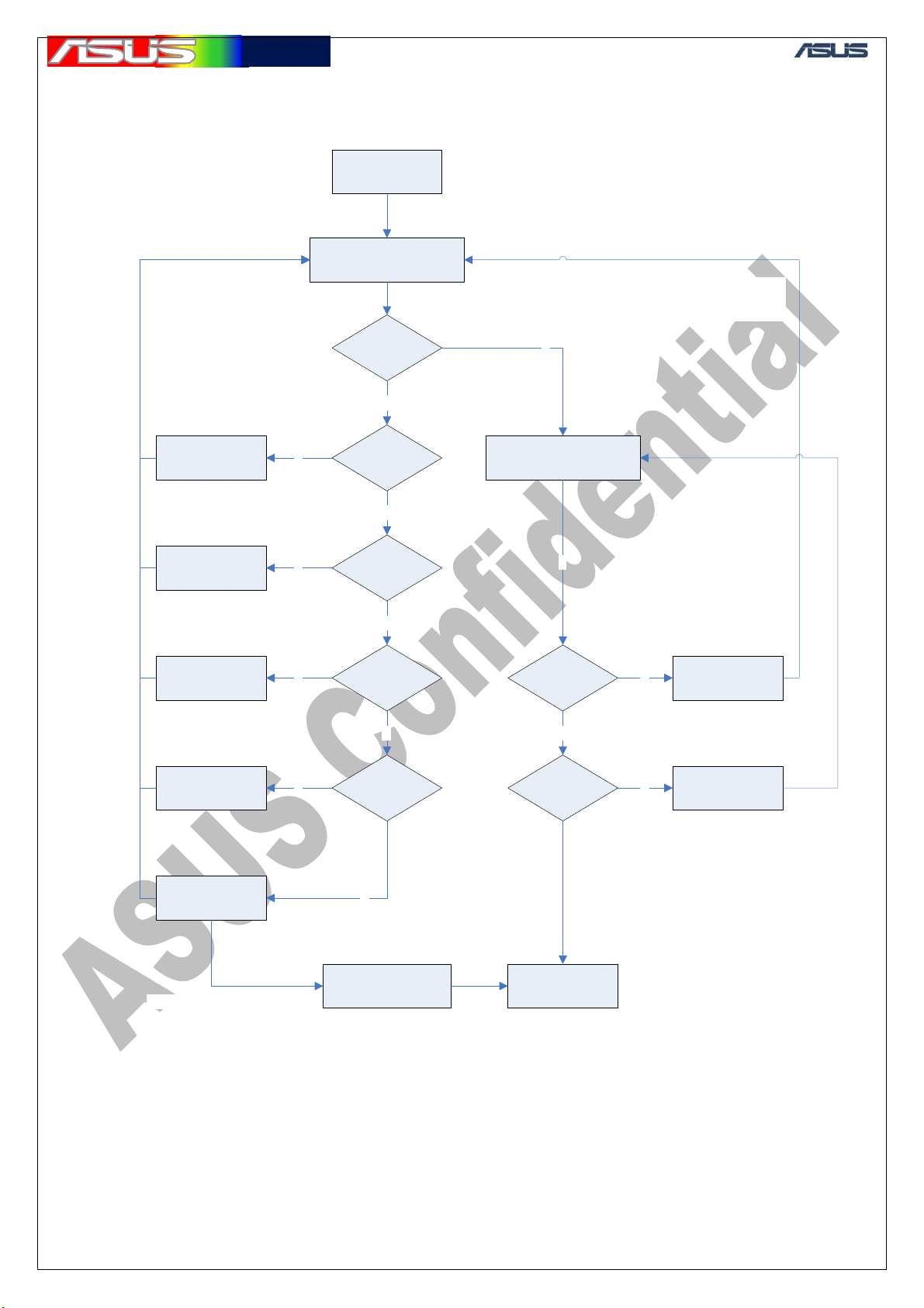
12.4 Blue tooth Test & Repair Procedure
GTC ■ Service Manual
50
Page 52

華華碩碩電電腦
腦
12.5 WIFI Test & Repair Procedure
Turn on PDA
Change WIFI
module
N
Turn on WIFI
ok?
Y
GTC ■ Service Manual
Search any
APs?
Y
NO
TROUBLE
FOUND
N
Disassemble
PDA
Check antenna
contact well
Y
PCB analysis
power supply
to WIFI
module
normal?
Y
N
N
Make sure
antenna
contact well
Change
components
Measure
signals
Output signal
normal?
Y
Assemble
PDA
51
N
Change WIFI
module
Page 53
華華碩碩電電腦
腦
13. Test Points Signal Examples
13.1 GSM900
Due to the spec of probe is not exactly the same please use the “working
sample” for signal reference.
GSM.ANT1:
GTC ■ Service Manual
GSM.ANT2 & GSM.TL1
52
Page 54
華華碩碩電電腦
腦
GSM.TL2 & GSM.TL3
GTC ■ Service Manual
GSM.RG1
53
Page 55

華華碩碩電電腦
腦
GSM.RG2
GTC ■ Service Manual
54
Page 56

華華碩碩電電腦
腦
GTC ■ Service Manual
13.2 DCS1800
Due to the spec of probe is not exactly the same please use the “working
sample” for signal reference.
GSM.ANT1
GSM.ANT2 & GSM.TH1
55
Page 57
華華碩碩電電腦
腦
GSM.TH2 & GSM.TH3
GTC ■ Service Manual
GSM.RD1
56
Page 58

華華碩碩電電腦
腦
GSM.RD2
GTC ■ Service Manual
57
Page 59

華華碩碩電電腦
腦
GTC ■ Service Manual
13.3 PCS1900
Due to the spec of probe is not exactly the same please use the “working
sample” for signal reference.
GSM.ANT1
GSM.ANT2 & GSM.TH1
58
Page 60

華華碩碩電電腦
腦
GSM.TH2 & GSM.TH3
GTC ■ Service Manual
GSM.RP1
59
Page 61

華華碩碩電電腦
腦
GSM.RP2
GTC ■ Service Manual
60
Page 62

華華碩碩電電腦
腦
GTC ■ Service Manual
13.4 WCDMA
Due to the spec of probe is not exactly the same please use the “working sample”
for signal reference.
WCDMA.ANT1
WCDMA.ANT2 (Tx)
61
Page 63

華華碩碩電電腦
腦
WCDMA.T1
GTC ■ Service Manual
WCDMA.T2
62
Page 64

華華碩碩電電腦
腦
WCDMA.T3
GTC ■ Service Manual
WCDMA.T4
63
Page 65

華華碩碩電電腦
腦
WCDMA.T5
GTC ■ Service Manual
WCDMA.ANT2 (Rx)
64
Page 66

華華碩碩電電腦
腦
WCDMA.R1
GTC ■ Service Manual
WCDMA.R2
65
Page 67

華華碩碩電電腦
腦
WCDMA.R3
GTC ■ Service Manual
66
Page 68

華華碩碩電電腦
腦
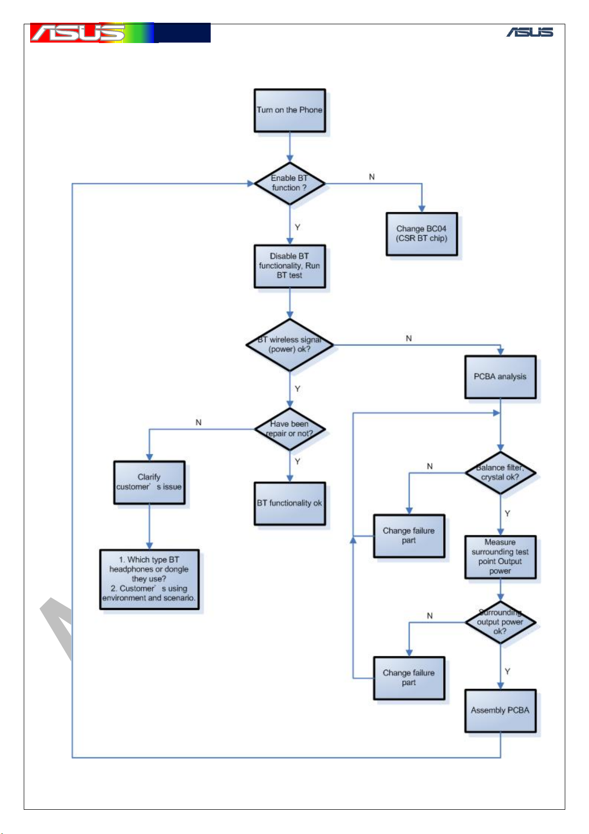
14. Blue tooth
Turn on the phone, make sure if BT can be enable.
(1) Confirm if BT is enabled or not
Touch here
GTC ■ Service Manual
BT Disable BT Enable and blue led flashed
(2)Turn off Blue tooth functionality:
Tap here
(3) BT test tool
TestCSR.exe
test.TXT
Put these two files above into PDA’s main directory (my device\)
67
Page 69

華華碩碩電電腦
腦
(4) Start BT test mode
Tap here
GTC ■ Service Manual
(5) Showing as the following menu. *
(i)
(iii)
(ii)
frequency
(i) First, turn on BT。
(ii) Enter test mode:
(iii) Choose a frequency
This option is used only for Anritsu885X series equipment
,press SETto start TX power
E.X. Frequency 2402:BT generate TX Power at2402MHz。
Frequency 2441:BT generate TX Power at2441MHz。
Frequency 2480:BT generate TX Power at2480MHz
68
。
Page 70

華華碩碩電電腦
腦
GTC ■ Service Manual
(6)Choose one frequency and measure power
(7) Measuring wireless performance via BT test program first. You may need to put the phone on shielding
box or TEM cell to insure no other interference. By comparing the golden sample’s normal output
value, you can judge the functionality of BT. Apparently, the wireless performance will differ within ±
2dBm. If the deviation of DUT is beyond the normal value, go straight for next step.
* The testing position should be the same with golden sample to reduce testing uncertainty.
8
BT Antenna in Bottom side
69
Page 71

華華碩碩電電腦
腦
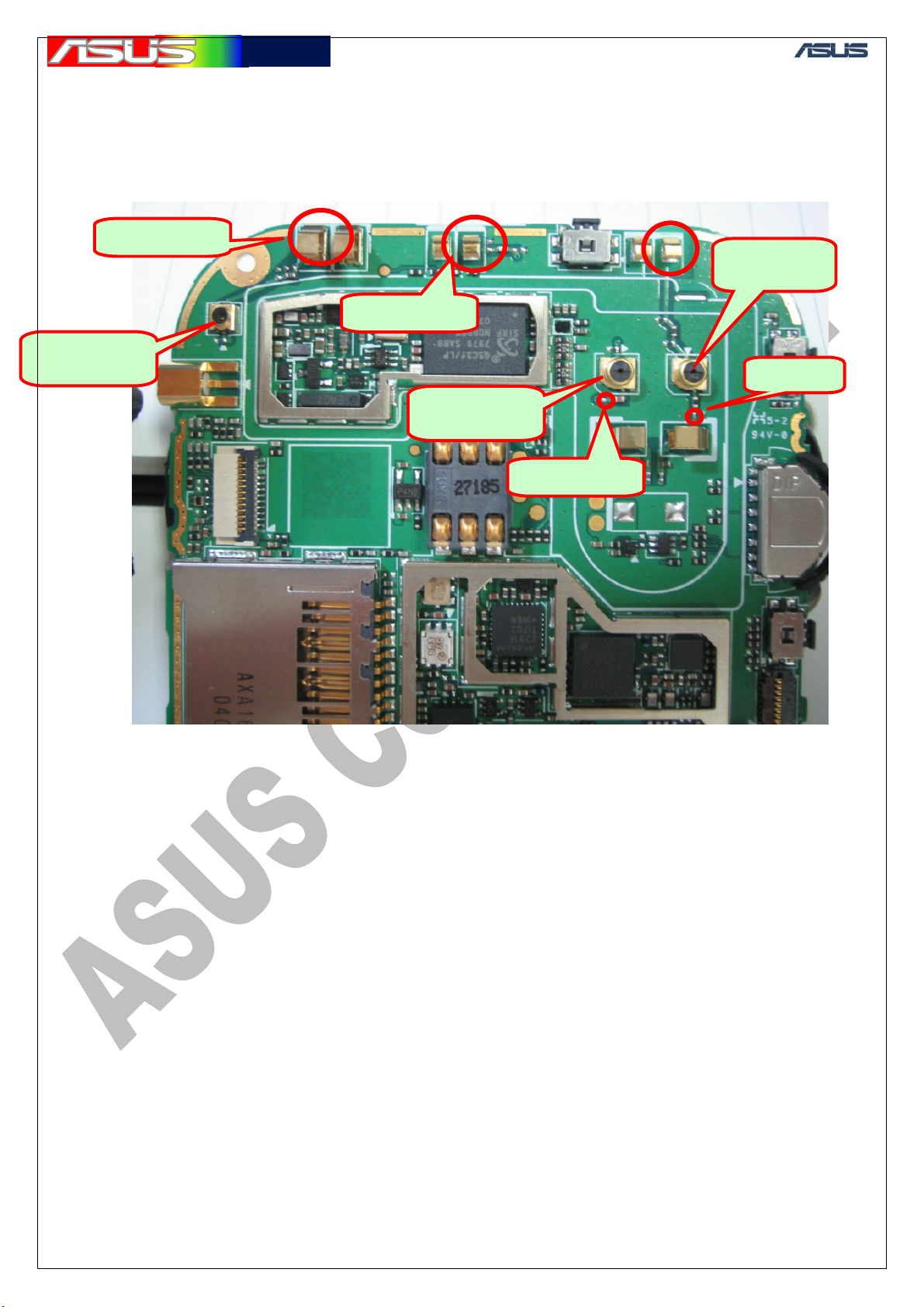
(8) BT position and testing point.
i. Make sure the RF probe is contact the resistor, BT output testing point1, (green circle) properly, the
output power will between -5 ~ +3 dBm normally.
ii. Next, measuring the BT output testing point2 (yellow circle) via RF probe, the output power will
between -5 ~ +3 dBm normally.
iii. If the output power still be abnormal, change the balance filter and go back to step ii.(You should
notice that the balance filter has its own orientation, so change it carefully.)
iv. Afterwards, the BT output power still be abnormal, change the BT chip.
.
GTC ■ Service Manual
BT Chip
BT Output
tesing point 1
Antenna
feed pin
Balance Filter
BT Output testing point 2
70
Page 72

華華碩碩電電腦
腦
15. WIFI
(1)
Turn on the phone, make sure if WIFI can be enable。
GTC ■ Service Manual
WIFI Disable WIFI Enable
(2)Searching AP:
SrartÆSettingsÆConnectionsÆWi-Fi manager
71
Page 73
華華碩碩電電腦
腦
(3)WIFI test mode
GTC ■ Service Manual
060518_u_00.00.18_d_0.05.01.05.zip 061024_pc_29_pda_28.zip
Unzip the above two files and put into PDA
execute
Go to another folder
Restart after installation
Tap AlpsRFtoolp
72
Page 74

華華碩碩電電腦
腦
.
The main menu is as above.
Settings are as above, you can choose
different channels then press start to
transmit power.
GTC ■ Service Manual
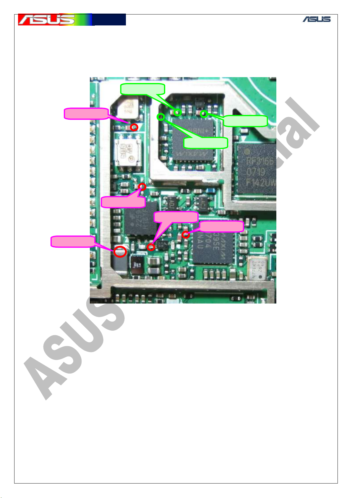
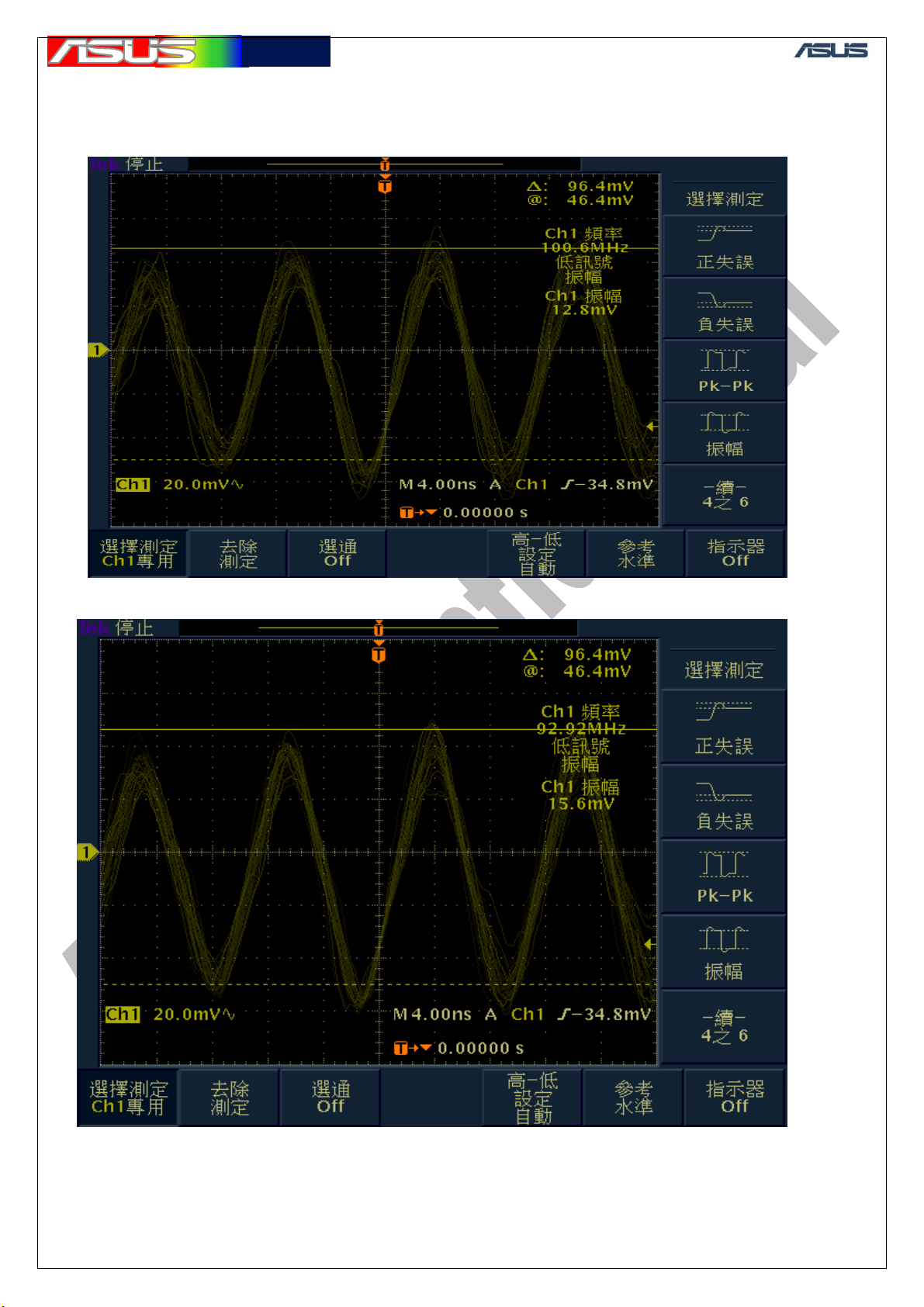
(4)Measure output power at test points
WIFI test point 1
WIFI test point 2
73
Page 75

華華碩碩電電腦
腦
GTC ■ Service Manual
Measure at test point1 typical power is about 13-15dBm.
If the power value is abnormal, change U35.
Measure at test point1 typical power is about 11-13dBm
If the power value is abnormal, change U30.
74
Page 76
華華碩碩電電腦
腦
GTC ■ Service Manual
16. Appendix
16.1 Typical Value of GSM/GPRS Conductive Tx/Rx Test
GSM/GPRS Tx Typical Value
Band Channel No.
975 880.2
EGSM 900
DCS1800
PCS1900
Band Channel No.
EGSM 900
DCS1800
PCS1900
62 902.4
124 914.8
512 1710.2
700 1747.8
885 1784.8
512 1850.2
661 1880
810 1909.8
975 925.2
62 947.4
124 959.8
512 1805.2
700 1842.8
885 1879.8
512 1930.2
661 1960
810 1989.8
Frequency.
(MHz)
GSM/GPRS Rx Typical Value
Frequency.
(MHz)
Power Level
5 32.5 +/- 1
0 29.5
0
Sensitivity Level - BER < 2% (dBm)
Typical Output Power
(dBm)
29.5 +/- 1
Maximum
-104
-103
-103
Tolerence
(dB)
+/- 1
16.2 Typical Value of WCDMA Conductive Tx/Rx Test
WCDMA Tx Typical Value
Band Channel No.
9612 1922.4
WCDMA Tx
Band Channel No.
WCDMA Rx
9750 1950
9888 1977.6
10562 2112.4
10700 2140
10838 2167.6
Frequency.
(MHz)
WCDMA Rx Typical Value
Frequency.
(MHz)
Power L evel
Maximum
(all up bit)
Sensitivity Level - BER < 0.1% (dBm)
Typical Output Power
(dBm)
23.5 +/- 1.5
Maximum
-111
Tolerence
(dB)
75
Page 77

華華碩碩電電腦
腦
16.3 Tx Test Environment Setup
Equipments Required:
1. PC
2. Specific Fixture for repair and test, including
A. Hermon USB contact
B. Power Supply contact
3. RF Probe with DC block and RF cable (30cm)
4. Spectrum Analyzer
5. Digital Multi-meter
Example of Tx Test Environment Setup:
GTC ■ Service Manual
76
Page 78

華華碩碩電電腦
腦
16.4 Rx Test Environment Setup
Equipments Required:
1. PC
2. Specific Fixture for repair and test, including
A. Hermon USB contact
B. Power Supply contact
C. RF connector and RF cable
3. RF Probe with DC block and RF cable (30cm)
4. Signal Generator
Example of Rx Test Environment Setup:
GTC ■ Service Manual
77
Page 79

華華碩碩電電腦
腦
GTC ■ Service Manual
17. GPS Introduce Purpose:
The Service Colleagues would be able to identify the GPS hardware trouble
issues of Solaris and then repair the hardware trouble issues soon.
17.1 Equipment requires
For identifying and repairing the GPS hardware trouble issues
of Solaris
17.2 Software:
SiRFDemoPPC, GPS Firmware: GSW3.2.4 or GSW Instant fix 3.2.4
17.3 Hardware:
GPS active antenna, Oscilloscope, GPS signal generator, Digital
Multimeter
78
Page 80
華華碩碩電電腦
腦
18. GPS Test points & Schematic
18.1 GPS Active Path
CON801
MMCX_JACK_1P
11GND1
GND2
2
3
L802
33NH
12
C802
100PF/50V
R803
+2.85V_GPS_LNA
12
C806
0.1UF/10V
C814
1 2
100PF/50V
10KOhm
1 2
1 2
21
10Ohm
3
Load
1
1
2
3
+2.85V_GPS_RF
R802
2
U802
Vin
ZXCT1009FTA
Iout
U803
1
A1
2
GND
3
A2
NC7WZ04L6X
U807
OUTPUT1
GND
OUTPUT2
UPG2179TB
R802
VCC
Vcont1
INPUT
Vcont2
GTC ■ Service Manual
+2.85V_GPS_RF_1
Y1
Y2
6
5
4
ACT_ANT_OFF
U807 pin 6
6
5
4
C817
1 2
100PF/50V
U807 pin 5
79
Page 81

華華碩碩電電腦
腦
18.2 Passive Path
GTC ■ Service Manual
4
OUTPUT
3
1575.42MHz
C823
L801
2.7NH
C803
1.2NH
21
1
IN
3
4
OUT
2
U809
1
C831
1 2
NC
RF_CON_4P
5
GND3
INPUT
GND12GND2
J801
21
100PF/50V
C822
1 2
12
C823
NC
C801
1 2
21
100PF/50V
L870
12NH
12
NC
C824
U806
GND34VCC
3
GND2
2
INPUT
1
GND1
UPC8215TU-E2
F805
1
1
SQ_37
F806
1
SQ_37
1
GND4
OUTPUT
GND5
5
6
7
8
+2.85V_GPS_BB
C807 C803
R889
0Ohm
1 2
12
C820
NC
C807
100PF/50V
12
+2.85V_GPS_LNA
12
C806
0.1UF/10V
C814
1 2
100PF/50V
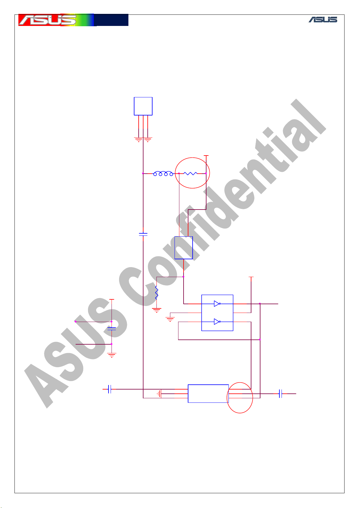
18.3 GPS Chip
+2.85V_GPS_RF_1
12
C808
0.01UF/16V
C816
33PF/50V
L805
4.7nH
2 1
TCXO_OUT
C821
80
12
+1.5V_GPS_RTC
12
12
C821
1000PF/50V
GPS_RTC
C825
GPS_BOOTSEL{13}
C809
1000PF/16V
+2.85V_GPS_RF_1
1000PF/16V
GPS_XTAL_O
GPS_XTAL_I
R811
VDDK1
VDDK2
RXA
RXB
ECLK
SCLK
MOE#
MWE#
SS#[0]
SS#[1]
GPIO[0]
ODO
EIT[0]
CS_F#
CS[0]#
TMODE
JTDO
JTDI
JTCK
JTRST#
JTMS
TXA
TXB
SO
SK
RIN
SI
B4
A10
C5
B3
C4
F7
B10
C10
A5
A6
C7
B7
A7
A8
B8
C8
J10
G10
B1
P1
D1
B2
J9
H1
A4
A2
J6
J8
J7
C6
B5
A3
D3
F1
C1
E1
E7
D10
M1
J1
N1
K1
L1
E10
F10
+1.5V_GPS_RTC
GPS_SPI_CS#
GPS_LNAPWR_EN
GPS_SPI_DO
GPS_SPI_DI
GPS_SPI_CLK
GPS_CS#
JTRST#
JTMS
N3
N10
N9
GND_RF10N4GND_RF11N5GND_RF12N6GND_RF13N7GND_RF14N8GND_RF15
P7
GND_RF7
GND_RF16P5GND_RF17
J3
F6
U804
GND_RF1L4GND_RF2L5GND_RF3L6GND_RF4L7GND_RF5L8GND_RF6L9GND_RF8N2GND_RF9
12
C810
100PF/50V
1 2C818 1000PF/16V
GPS_RST_RF#
SIGN_MAG
CLKACQ
C825
12
100KOhm
M10
VCC_RF1
M9
VCC_RF9
M8
VCC_RF8
M7
VCC_RF7
M6
VCC_RF6
M5
VCC_RF5
M4
VCC_RF4
M3
VCC_RF3
M2
VCC_RF2
P4
TP_IF
P8
NC
P9
VCC_RTC
P6
RFIN
P3
XTAL_OUT
P2
XTAL_IN
H6
PLL_FILTER
H10
1 2
RESET#
K6
SPI_DO
K8
SPI_DI
K7
SPI_CLK
K9
SPI_CEB
K3
AGCPWM
K5
SIGN_MAG_O
J5
SIGN_MAG_I
K4
CLKACQ_O
J4
CLKACQ_I
K10
RTC_OUT
L10
RTC_XO
P10
RTC_XI
A9
*EA[0]
B9
*EA[1]
D7
*EA[2]
C9
*EA[3]
B6
*EA[4]
D8
*EA[5]
D9
*EA[6]
E8
*EA[7]
E9
*EA[8]
G9
*EA[9]
H9
*EA[10]
G8
*EA[11]
H8
*EA[12]
G7
*EA[13]
H7
*EA[14]
G6
*EA[15]
G5
*EA[16]
H5
*EA[17]
F8
*EA[18]
F9
*EA[19]
ED[0]G1ED[1]C2ED[2]F3ED[3]F2*ED[4]D2*ED[5]H2*ED[6]H4ED[7]J2*ED[8]E3*ED[9]E2*ED[10]C3*ED[11]G3*ED[12]G2*ED[13]H3*ED[14]G4*ED[15]
GSC3F
GPS_ED0
GPS_ED1
GPS_ED2
GPS_ED3
GPS_ED7
GPS_SPI_DO
GPS_SPI_DI GPS_RST_RF#
GPS_SPI_CLK
GPS_SPI_CS#
R811
L3
VDD_BB1D4VDD_BB2E4VDD_BB3F4VDD_BB4K2VDD_BB5L2VDD_BB6
GND_BB1A1GND_BB2D5GND_BB3D6GND_BB4E5GND_BB5E6GND_BB6F5GND_BB7
VDD_RTC
VDDPLL_O
VDD_PLL
VDD_FLASH
VDD_REG1
VDD_REG2
Reserved1
Reserved2
SRESET#
ON_OFF
RFPWRUP
GRFRST#
TIMEMARK
GPIO[13]
GPIO[14]
GPIO[15]
WAKEUP#
Reserved3
C805 0.01UF/16V
1 2
C811 10UF/6.3V
1 2
GPS_TX {13}
GPS_RX {13}
GPS_RST# {13}
GPS_ON_OFF
GPS_RFPWR_EN
GPS_EIT
1 2R812 100KOhm
1 2R808 100KOhm
1 2R809 100KOhm
GPS_RTC
+2.85V_GPS_BB
+2.85V_GPS_BB
Page 82

華華碩碩電電腦
腦
GTC ■ Service Manual
18.4 Power part test points
GPS_PWR_EN{13}
R813
RF_VBAT{13}
GPS_RFPWR_EN
12
R813
100KOhm
12
C832
10UF/6.3V
GPS_LNAPWR_EN_OUT
12
C819
0.1UF/10V
U811
A1
INA
A4
INB
A2
SHDNA#
A3
SHDNB#
MAX8559EBAJJ
OUTA
OUTB
BP
GND
B1
B4
B2
B3
12
C833
0.01UF/16V
C830
10UF/6.3V
10UF/6.3V
12
C830
+2.85V_GPS_LNA
12
C834
C819
L806
1
1
22MHZ
C834
GND
3
+1.5V_GPS_RTC
BACKUP_BAT
C838
2.2UF/6.3V
1 2
U319
5
GND
4
3
VOUT
VIN
CE
XC6215B152GR
VSS
1
2
C839
1UF/10V
1 2
C839 C838
+2.85V_GPS_BB
RF_VBAT{13}
GPS_PWR_EN{13}
2
C836
2.2UF/10V
1
U318
C3
IN
A3
EN
TPS79328YZQR
OUT
NR
GND
C1
B2
A1
C837
1
2
C837
1000PF/50V
+2.85V_GPS_RF+2.85V_GPS_RF_1
2
2
18.5 Testing signal from base band
81
Page 83

華華碩碩電電腦
腦
19. Test points placement point
19.1 GPS Antenna
C823
C803
R813
C819
Test point displacement plot 1
C807
U807 pin6
R802
C838
GTC ■ Service Manual
R811
C821
C825
U807 pin4
Testing signal from baseband
T809T808
82
Page 84
華華碩碩電電腦
腦
N
GTC ■ Service Manual
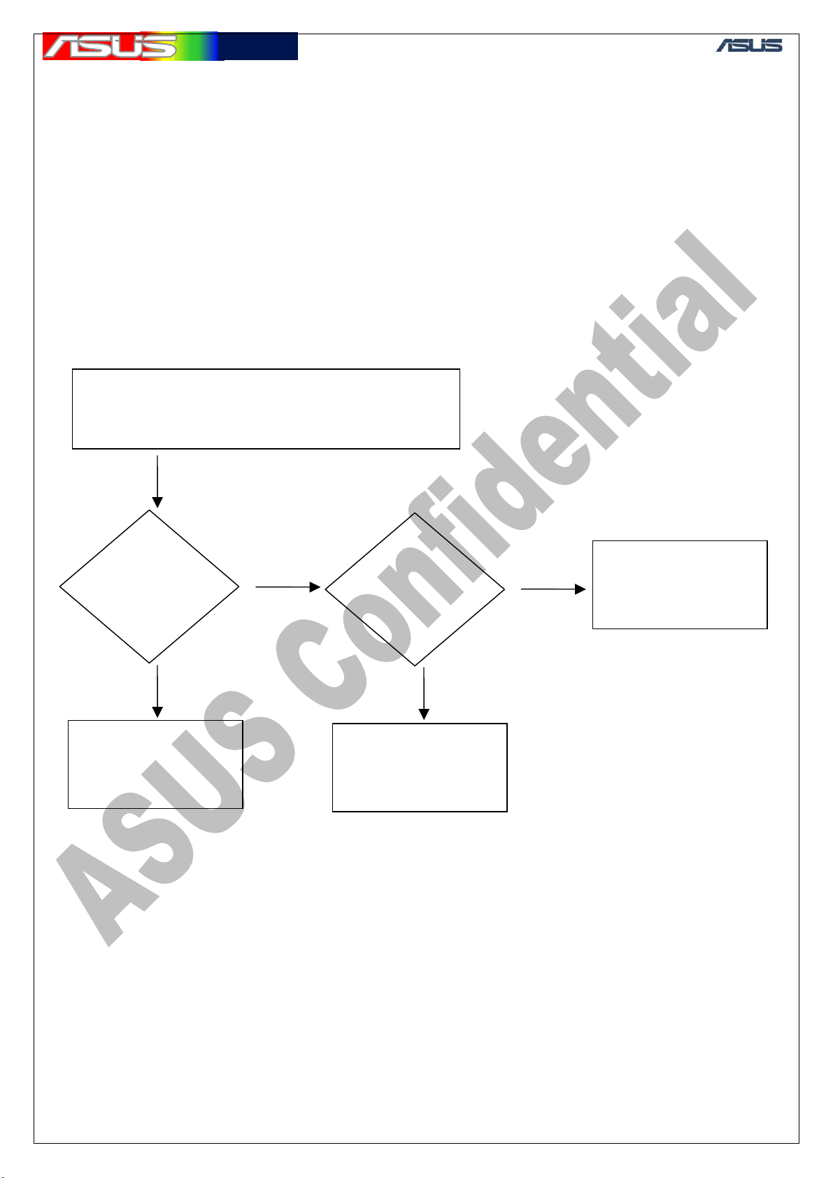
20. GPS Hardware Examination Procedure
The GPS examination procedure includes six parts. In the six parts, SiRFDemo
PPC program must be used. (Appendix A)
1. Start the SiRFDemoPPC program. Then, make sure that the GPS comport
setting is [Port:COM3][Baud Rate:4800 ]. After this step, check whether the
GPS function works or not.
Re-download the GPS firmware (as Appendix B) and then check if the GPS
function or works or not.
2. Active Path Fault Finding Chart
Put GSP active antenna into CON801 and then make
the active antenna near the window or open sky.(To
get the fine GPS signal)
YES
The C/N0 value
(got by the
SiRFDemo) > 35
YES
Do 4. Passive Path
Fault Finding Chart
O
Make sureU807
Pin6:Low(<0.2V)
Pin4:High(>2.5V)
OK?
YES
Do as SiRF StarIII
Fault Finding Chart
NO
Replace U807
with a new one
83
Page 85
華華碩碩電電腦
腦
g
d
n
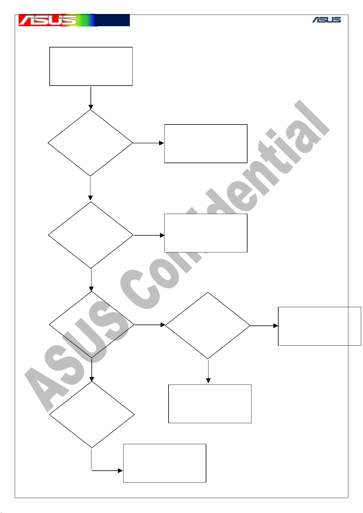
4.Passive Path Fault Finding Chart
GTC ■ Service Manual
Remove the GPS
active antenna
See if the GPS
antenna contacts
with the antenna
contact spring well?
Check if C803.Pin1 an
C823 Pin 1 get connectio
directly?
Make sure that the GPS
antenna contact well with
the sprin
YES
Change J801 with a
new one
YES
Check if the voltage of
C819 is 3±10% (V)?
Check if the voltage of
C807.Pin1 is 2.85±5%
(V)?
Do the Power Part
Fault Finding Chart
YES
YES
Check if the voltage
of C807.Pin1 is
2.85±5% (V) ?
Replace U801 with a
new one
YES
Replace U806 or do
SIRF StarIII Fault
Finding Chart
84
Page 86

華華碩碩電電腦
腦
N
t
N
N
N
t
5.Power Part Fault Finding Chart
Make sure the V_BAT
is 4V
GTC ■ Service Manual
C830 and C834
are 2.85±5%
YES
Check if
the voltage of
R813 >1.6V?
YES
Check if
(V) ?
O
O
Do SiRF StarIII Faul
Finding Chart or change
U318
Replace U811
with a new one
Check if the voltage of
C838 >1.5V?
Check if the
voltage of C839 is
1.5±5% (V)?
YES
YES
O
O
YES
V_bat is not on
Replace U319 with a
new one
Do SiRF StarIII Faul
Finding Chart
85
Page 87
華華碩碩電電腦
腦
NO N
N
N
6.SiRF StarIII Fault Finding Chart
GTC ■ Service Manual
Put the GPS active
antenna into CON301
YES
Checnk
C837(2.85V±5%)
C810(1.5V±5%)
OK?
YES
Measure
C821.Pin1
OK?
O
Do Power Part Fault
Finding Chart
Replace X802 with a
new one
YES
Measure
C406.Pin2
OK?
YES
Measure
T305
T306
OK?
YES
O
O
Replace
X3801 with new
ones
Replace U804
with a new one
Re-Download GPS
Firmware
86
Page 88
華華碩碩電電腦
腦
21. Measurement results of all test points
Test point : T808
GTC ■ Service Manual
Test point :T809
87
Page 89

華華碩碩電電腦
腦
Test point :C821
GTC ■ Service Manual
Test point :C825
88
Page 90

華華碩碩電電腦
腦
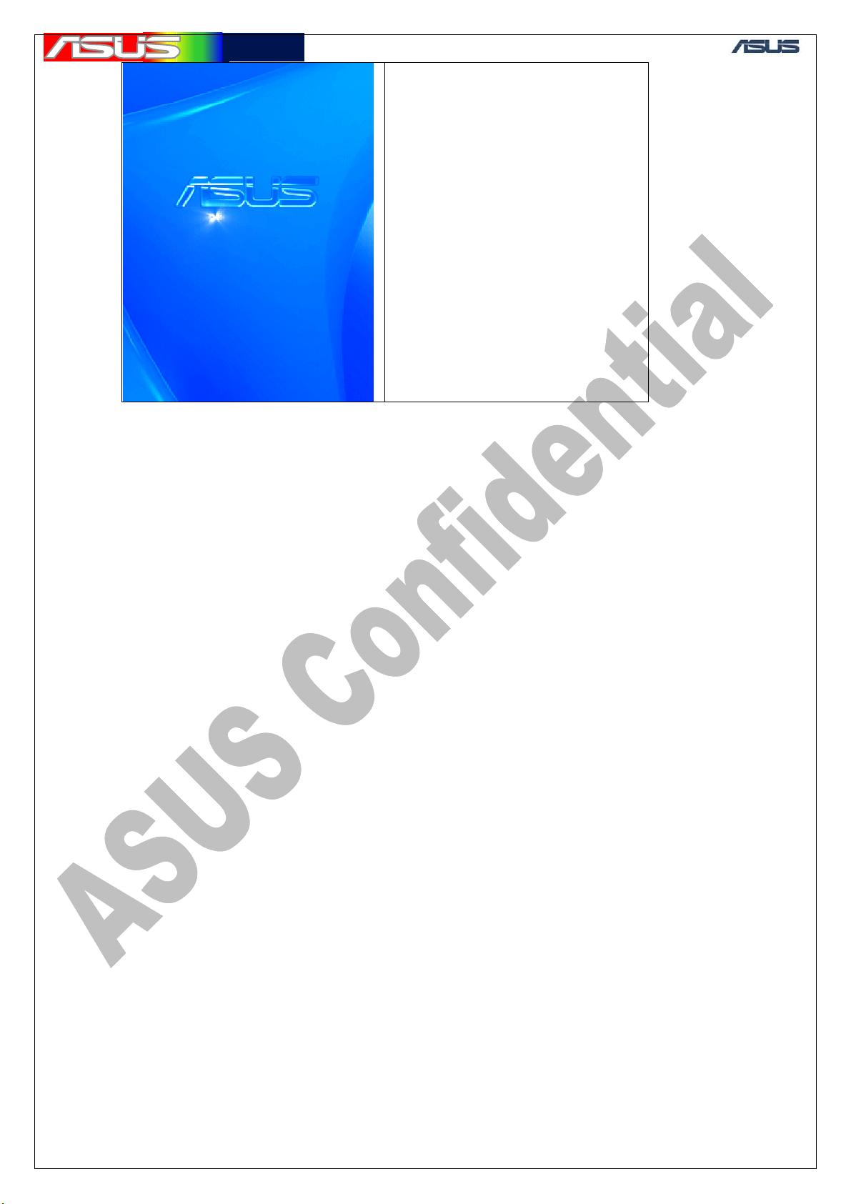
22. Software procedure
GTC ■ Service Manual
Put SIRFDemoPPC at Micro SD
Card
1. choose [SiRFDemoPPC]
2. choose [OK]
89
Page 91

華華碩碩電電腦
腦
GTC ■ Service Manual
1. choose [OK]
1. choose [Connect]
4800 or 57600
1. choose [Done]
90
Page 92

華華碩碩電電腦
腦
GTC ■ Service Manual
SiRFDemoPPC plantface
1.choose [Signal]
GPS signal receiving
91
Page 93

華華碩碩電電腦
腦
GTC ■ Service Manual
The green signal means the
signal has been demodulated.
When all tests are finished
1. choose [setup]
1. choose [Exit]
92
Page 94

華華碩碩電電腦
腦
GTC ■ Service Manual
93
Page 95

華華碩碩電電腦
腦
22.1 GPS firmware download
1.choose [Pegasus_DGPS.exe]
GTC ■ Service Manual
Re-download automatically
begins
The re-download is finished
94
Page 96
華華碩碩電電腦
腦
Mobile re-boot
GTC ■ Service Manual
95
 Loading...