

Page 1

Motherboard Layout
3
1
2
4
567
17.0cm (6.7 in)
JCFPWR1
1
HDMI1
29
28
27
26
DVI2
USB 2.0
T: U SB 0
B: USB1
1
VGA1
1
LVDS1
LAN2
LAN1
1
Line Out
Bottom:
Center:
Line In
Mic In
Top:
1
COM1
AUDIO
CODEC
25
COM2
24
ErP/EuP Ready
CON1
PCIE1
1
23
Super
IO
JGPIO1
IMB-142
PCI1
RoHS
22
21
CPU_FAN1 CHA_FAN2 CHA_FAN1
1
SMBUS1
16Mb
BIOS
1
USB4_51USB6_7
1
1
USB2_3
HDLED RESET
PANEL 1
1
Designedin Taipei
19
20
PLED PWRBTN
18
JPS2
CMOS
Battery
1
FSB800
DDR3_B1
DDR3_A1
SATAII_1
JPWR1
1
CLRCMOS1
SPEAKER1
16
17
17.0cm (6.7 in)
8
9
SATAII_2
10
11
12
SATAPWR1
13
14
1
15
1 JCF Power Connector (JCF PWR1) 16 Clear CMOS Jumper (CLRCMOS1)
2 ATX 12V Power Connector (ATX12V1) 17 Chassis Speaker Header
3 CPU Fan Connector (CPU_FAN1) (SPEAKER 1, White)
4 Chassis Fan Connector (CHA_FAN2) 18 JPS Connector (JPS2)
5 Chassis Fan Connector (CHA_FAN1) 19 USB 2.0 Header (USB2_3, Blue)
6 CPU Heatsink 20 USB 2.0 Header (USB4_5, Blue)
7 2 x DDR3 DIMM Slots 21 Chipset Heatsink
8 16Mb Flash 22 PCI Slot (PCI1)
9 SMBUS Connector (SMBUS1) 23 JGP IO Connector (JGP IO1)
10 SATA2 Connector (SATAII_1, Blue) 24 COM Port Header (COM1)
11 SATA2 Connector (SATAII_2, Red) 25 COM Port Header (COM2)
12 USB 2.0 Header (USB6_7, Blue) 26 PCI Express x1 Slot (PCIE1, White)
13 JPWR Connector (JPWR1) 27 LVDS Connector (LVDS1)
14 SATA Power Connector (SATAPWR1) 28 CON1
15 System Panel Header (PANEL1, White) 29 VGA Header (VGA1)
1
Page 2

Jumpers Setup
The illustration shows how jumpers are
setup. When the jumper cap is placed on
pins, the jumper is “Short”. If no jumper cap
is placed on pins, the jumper is “Open”. The
illustration shows a 3-pin jumper whose
pin1 and pin2 are “Short” when jumper cap
is placed on these 2 pins.
Jumper Setting Description
Clear CMOS Jumper
(CLRCMOS1)
(see p.1, No. 16)
Note: CLRCMOS1 allows you to clear the data in CMOS. To clear and reset the
system parameters to default setup, please turn off the computer and unplug
the power cord from the power supply. After waiting for 15 seconds, use a
jumper cap to short pin2 and pin3 on CLRCMOS1 for 5 seconds. However,
please do not clear the CMOS right after you update the BIOS. If you need
to clear the CMOS when you just fi nish updating the BIOS, you must boot up
the system fi rst, and then shut it down before you do the clear-CMOS action.
Please be noted that the password, date, time, user default profi le and MAC
address will be cleared only if the CMOS battery is removed.
Clear CMOSDefault
2
Page 3
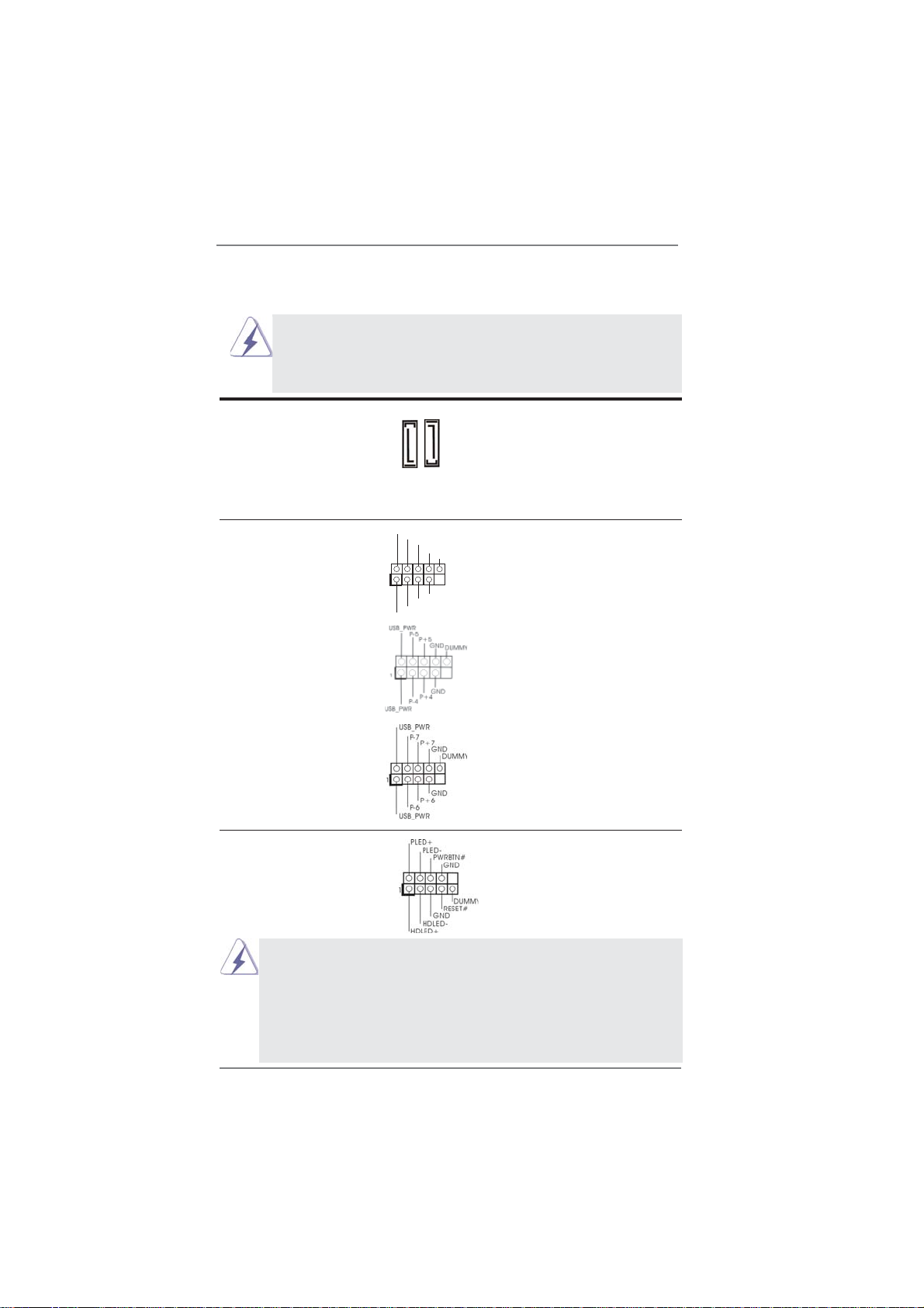
Onboard Headers and Connectors
Onboard headers and connectors are NOT jumpers. Do NOT place
jumper caps over these headers and connectors. Placing jumper caps
over the headers and connectors will cause permanent damage of the
motherboard!
SATAII Connectors These two Serial ATAII
(SATAII_1: see p.1, No. 10)
(SATAII_2: see p.1, No. 11)
storage devices. The current
SATAII interface allows up to
3.0 Gb/s data transfer rate.
(SATAII) connectors support
SATAII_1 SATAII_2
SATA data cables for internal
1
USB_PWR
P-3
P-2
USB_PWR
P+3
P+2
GND
GND
DUMMY
USB 2.0 Headers Besides two default USB 2.0
(9-pin USB2_3)
(see p.1 No. 19)
ports on the I/O panel, there
are three USB 2.0 headers on
this motherboard. Each
USB 2.0 header can support
two USB 2.0 ports.
(9-pin USB4_5)
(see p.1 No. 20)
(9-pin USB6_7)
(see p.1 No. 12)
System Panel Header This header accommodates
(9-pin PANEL1)
(see p.1 No. 15)
several system front panel
functions.
Connect the power switch, reset switch and system status indicator on the
chassis to this header according to the pin assignments below. Note the
positive and negative pins before connecting the cables.
PWRBTN (Power Switch):
Connect to the power switch on the chassis front panel. You may confi gure
the way to turn off your system using the power switch.
3
Page 4
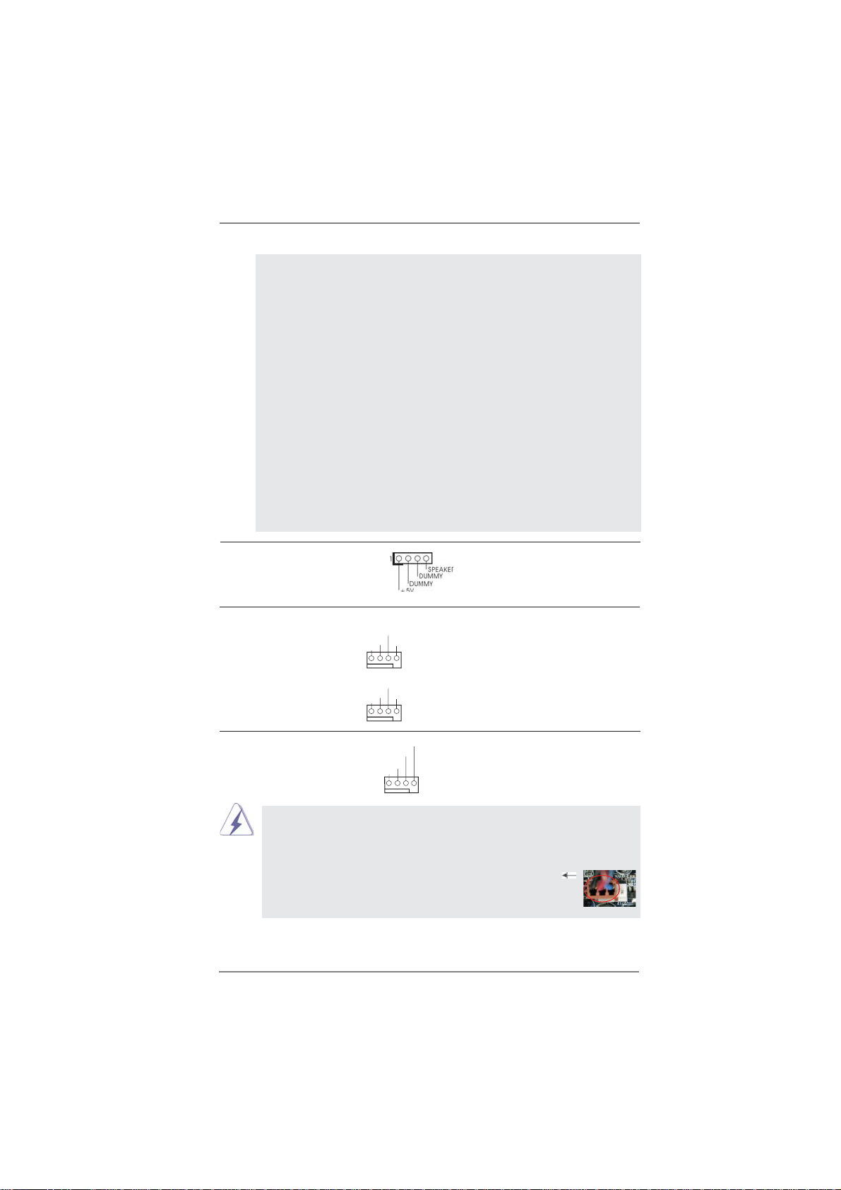
RESET (Reset Switch):
Connect to the reset switch on the chassis front panel. Press the reset
switch to restart the computer if the computer freezes and fails to perform a
normal restart.
PLED (System Power LED):
Connect to the power status indicator on the chassis front panel. The LED
is on when the system is operating. The LED keeps blinking when the sys-
tem is in S1 sleep state. The LED is off when the system is in S3/S4 sleep
state or powered off (S5).
HDLED (Hard Drive Activity LED):
Connect to the hard drive activity LED on the chassis front panel. The LED
is on when the hard drive is reading or writing data.
The front panel design may differ by chassis. A front panel module mainly
consists of power switch, reset switch, power LED, hard drive activity LED,
speaker and etc. When connecting your chassis front panel module to this
header, make sure the wire assignments and the pin assign-ments are
matched correctly.
Chassis Speaker Header Please connect the chassis
(4-pin SPEAKER 1)
(see p.1 No. 17)
speaker to this header.
Chassis Fan Connectors Please connect the fan cables
(4-pin CHA_FAN1)
(see p.1 No. 5)
to the fan connectors and
match the black wire to the
CHA_FAN_SPEED
+12V
FAN_SPEED_CONTROL
GND
ground pin.
(4-pin CHA_FAN2)
(see p.1 No. 4)
CPU Fan Connectors Please connect the CPU fan
(4-pin CPU_FAN1)
(see p.1 No. 3)
cable to the connector and
match the black wire to the
ground pin.
Though this motherboard provides 4-Pin CPU fan (Quiet Fan) support, the 3-Pin
CPU fan still can work successfully even without the fan speed control function.
If you plan to connect the 3-Pin CPU fan to the CPU fan connector on this
motherboard, please connect it to Pin 1-3.
CHA_FAN_SPEED
+12V
FAN_SPEED_CONTROL
GND
FAN_SPEED_CONTROL
CPU_FAN_SPEED
+12V
GND
1 2 3 4
Pin 1-3 Connected
3-Pin Fan Installation
4
Page 5
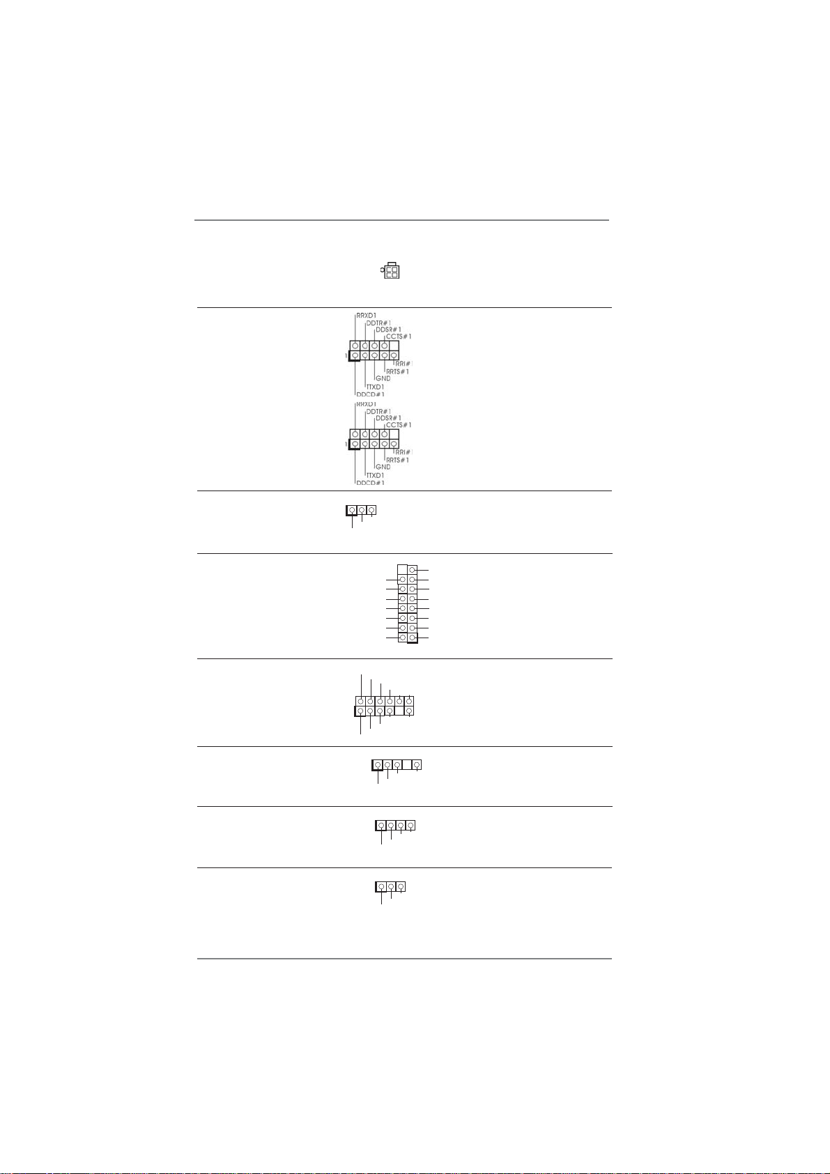
ATX 12V Power Connector Please connect an ATX 12V
(4-pin ATX12V1)
(see p.1 No. 2)
power supply to this connector.
Serial port Headers Each COM1 header supports a
(9-pin COM1)
(see p.1 No. 24)
(9-pin COM2)
(see p.1 No. 25)
serial port module.
JCF Power Connector
(3-pin JCF PWR1)
(see p.1 No. 1)
D-SUB VGA Connector
(15-pin VGA1)
(see p.1 No. 29)
JGP IO Connector
(11-pin JGP IO1)
(see p.1 No. 23)
JPS Connector
(4-pin JPS2)
(see p.1 No. 18)
JPWR Connector
(4-pin JPWR_1)
(see p.1 No. 13)
SATA Power Connector
(3-pin SATA PWR_1)
(see p.1 No. 14)
1
+5V
CF SocketPower (Con1)
+3V
Dsub VSYNC
Dsub DDCDATA
GND
GND
GND
N/A
Dsub_G
GPIO0
GPIO1
1
GPI 5O
GPIO4
1
PS2 VCC
1
+5V
1
+5V
1
GPIO2
GPIO3
GPIO Power
+5V
+3V
GPIO7
GPIO6
KBDATA
KBCLK
+12V
GND
GND
GND
SATA 7thPin Power
GND
Dsub DDCCLK
Dsub HSYNC
N/A
VGA PWR
GND
GND
Dsub_B
Dsub_R
5
Page 6
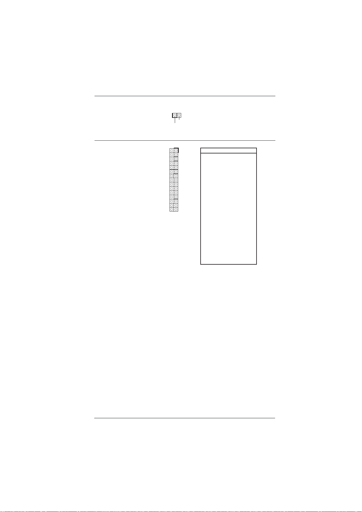
SMBUS Connector
(2-pin SMBUS1)
(see p.1 No. 9)
1
SMBUS DATA
SMBUS CLK
LVDS Connector
(30-pin LVDS1)
(see p.1 No. 27)
1
2
LVDS Connector Pin Defi nition
Pin 1, 2, 3, 4 : Backlight PWR
Pin 5, 6, 11, 17, 18, 29, 30 : GND
Pin 7, 9 : LCD VDD PWR Enable
Pin 8 : LCD PID1
Pin 10 : LCD PID0
Pin 12 : EDID CLK
Pin 13 : Backlight Enable
Pin 14 : EDID DATA
Pin 15 : Backlight PWM
29
30
Pin 16 : EDID CS#
Pin 19 : EDID PWR(3V)
Pin 20 : Empty
Pin 21 : LVDS CLK#
Pin 22 : LVDS CLK
Pin 23 : LVDS DATA2#
Pin 24 : LVDS DATA2
Pin 25 : LVDS DATA1#
Pin 26 : LVDS DATA1
Pin 27 : LVDS DATA0#
Pin 28 : LVDS DATA0
6
 Loading...