

Page 1

G41M-VS
User Manual
Version 1.0
Published August 2009
Copyright©2009 ASRock INC. All rights reserved.
11
1
11
Page 2

Copyright Notice:Copyright Notice:
Copyright Notice:
Copyright Notice:Copyright Notice:
No part of this manual may be reproduced, transcribed, transmitted, or translated in
any language, in any form or by any means, except duplication of documentation by
the purchaser for backup purpose, without written consent of ASRock Inc.
Products and corporate names appearing in this manual may or may not be regis-
tered trademarks or copyrights of their respective companies, and are used only for
identification or explanation and to the owners’ benefit, without intent to infringe.
Disclaimer:Disclaimer:
Disclaimer:
Disclaimer:Disclaimer:
Specifications and information contained in this manual are furnished for informa-
tional use only and subject to change without notice, and should not be constructed
as a commitment by ASRock. ASRock assumes no responsibility for any errors or
omissions that may appear in this manual.
With respect to the contents of this manual, ASRock does not provide warranty of
any kind, either expressed or implied, including but not limited to the implied warran-
ties or conditions of merchantability or fitness for a particular purpose.
In no event shall ASRock, its directors, officers, employees, or agents be liable for
any indirect, special, incidental, or consequential damages (including damages for
loss of profits, loss of business, loss of data, interruption of business and the like),
even if ASRock has been advised of the possibility of such damages arising from any
defect or error in the manual or product.
This device complies with Part 15 of the FCC Rules. Operation is subject to the
following two conditions:
(1) this device may not cause harmful interference, and
(2) this device must accept any interference received, including interference that
may cause undesired operation.
CALIFORNIA, USA ONLY
The Lithium battery adopted on this motherboard contains Perchlorate, a toxic
substance controlled in Perchlorate Best Management Practices (BMP) regulations
passed by the California Legislature. When you discard the Lithium battery in
California, USA, please follow the related regulations in advance.
“Perchlorate Material-special handling may apply, see
www.dtsc.ca.gov/hazardouswaste/perchlorate”
ASRock Website: http://www.asrock.com
22
2
22
Page 3

ContentsContents
Contents
ContentsContents
1 Introduction1 Introduction
1 Introduction
1 Introduction1 Introduction
1.1 Package Contents .......................................................... 5
1.2 Specifications ................................................................ 6
1.3 Motherboard Layout ........................................................ 10
1.4 I/O Panel......................................................................... 11
2 Installation2 Installation
2 Installation
2 Installation2 Installation
2.1 Screw Holes ................................................................... 12
2.2 Pre-installation Precautions ............................................ 12
2.3 CPU Installation .............................................................. 13
2.4 Installation of Heatsink and CPU fan ............................... 15
2.5 Installation of Memory Modules (DIMM) ......................... 16
2.6 Expansion Slots (PCI and PCI Express Slots) ..................... 17
2.7 Jumpers Setup ............................................................... 18
2.8 Onboard Headers and Connectors .................................. 20
2.9 SATAII Hard Disk Setup Guide ........................................ 23
2.10 Serial ATA (SATA) / Serial ATAII (SATAII) Hard Disks
Installation ...................................................................... 24
2.11 Driver Installation Guide .............................................. 24
2.12 Untied Overclocking Technology .................................... 24
3 BIOS S3 BIOS S
3 BIOS S
3 BIOS S3 BIOS S
ETUP UTILITYETUP UTILITY
ETUP UTILITY
ETUP UTILITYETUP UTILITY
3.1 Introduction ..................................................................... 25
3.1.1 BIOS Menu Bar ..................................................... 25
3.1.2 Navigation Keys .................................................... 26
3.2 Main Screen ................................................................... 26
3.3 OC Tweaker Screen ...................................................... 27
3.4 Advanced Screen ......................................................... 35
3.4.1 CPU Configuration ................................................ 36
3.4.2 Chipset Configuration .......................................... 38
3.4.3 ACPI Configuration ............................................... 40
3.4.4 Storage Configuration ......................................... 41
3.4.5 PCIPnP Configuration ........................................... 43
3.4.6 Super IO Configuration ........................................ 44
3.4.7 USB Configuration ............................................... 45
3.5 Hardware Health Event Monitoring Screen .................. 46
3.6 Boot Screen ................................................................... 47
3.6.1 Boot Settings Configuration .................................. 47
3.7 Security Screen ............................................................ 48
3.8 Exit Screen .................................................................... 49
......................................................................................................
...................................................
......................................................................................................
..........................................................................................................
.....................................................
..........................................................................................................
....................................................................................
..........................................
....................................................................................
5 5
5
5 5
12 12
12
12 12
25 25
25
25 25
33
3
33
Page 4

4 Software Support4 Software Support
4 Software Support
4 Software Support4 Software Support
4.1 Install Operating System ............................................... 50
4.2 Support CD Information ................................................. 50
4.2.1 Running Support CD ............................................ 50
4.2.2 Drivers Menu ........................................................ 50
4.2.3 Utilities Menu ........................................................ 50
4.2.4 Contact Information .............................................. 50
......................................................................................
...........................................
......................................................................................
50 50
50
50 50
44
4
44
Page 5

Chapter 1 IntroductionChapter 1 Introduction
Chapter 1 Introduction
Chapter 1 IntroductionChapter 1 Introduction
Thank you for purchasing ASRock G41M-VS motherboard, a reliable motherboard
produced under ASRock’s consistently stringent quality control. It delivers excellent
performance with robust design conforming to ASRock’s commitment to quality and
endurance.
In this manual, chapter 1 and 2 contain introduction of the motherboard and step-by-step
guide to the hardware installation. Chapter 3 and 4 contain the configuration guide to
BIOS setup and information of the Support CD.
Because the motherboard specifications and the BIOS software might be
updated, the content of this manual will be subject to change without
notice. In case any modifications of this manual occur, the updated
version will be available on ASRock website without further notice. You
may find the latest VGA cards and CPU support lists on ASRock website
as well. ASRock website
If you require technical support related to this motherboard, please visit
our website for specific information about the model you are using.
www.asrock.com/support/index.asp
1.1 P1.1 P
ackack
1.1 P
1.1 P1.1 P
ASRock G41M-VS Motherboard
(Micro ATX Form Factor: 8.8-in x 6.7-in, 22.4 cm x 17.0 cm)
ASRock G41M-VS Quick Installation Guide
ASRock G41M-VS Support CD
One 80-conductor Ultra ATA 66/100 IDE Ribbon Cable (Optional)
One Serial ATA (SATA) Data Cable (Optional)
One I/O Panel Shield
age Contentsage Contents
ack
age Contents
ackack
age Contentsage Contents
http://www.asrock.com
55
5
55
Page 6
1.21.2
SpecificationsSpecifications
1.2
Specifications
1.21.2
SpecificationsSpecifications
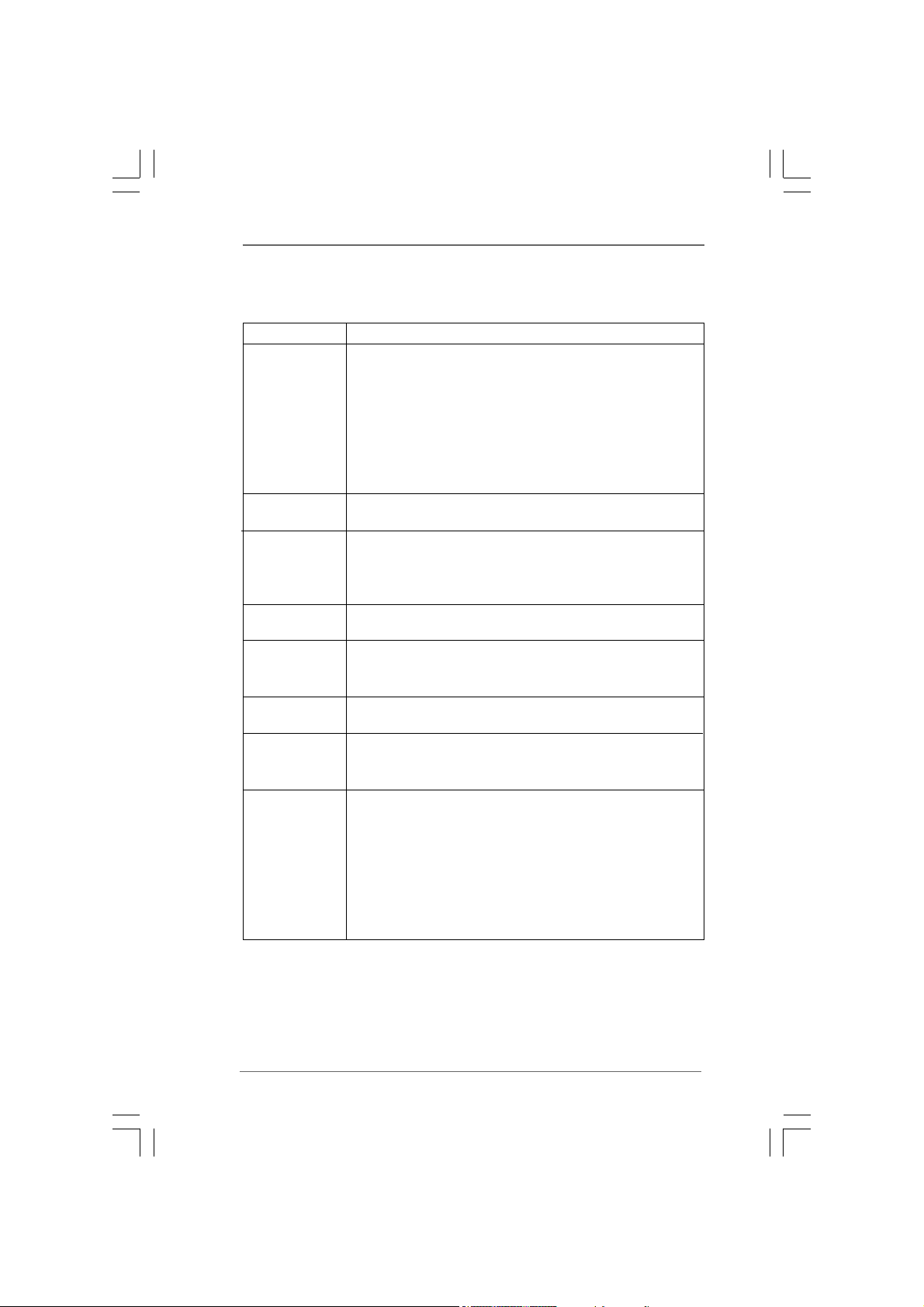
Platform - Micro ATX Form Factor: 8.8-in x 6.7-in, 22.4 cm x 17.0 cm
CPU - LGA 775 for Intel
®
CoreTM 2 Quad / CoreTM 2 Duo / Pentium
Dual Core / Celeron® Dual Core / Celeron®, supporting Dual
Core Wolfdale processors (see CAUTION 1)
- Supports CPU power up to 65W
- Supports FSB1333/1066/800 MHz
- Supports Hyper-Threading Technology (see CAUTION 2)
- Supports Untied Overclocking Technology (see CAUTION 3)
- Supports EM64T CPU
Chipset - Northbridge: Intel
®
G41
- Southbridge: Intel® ICH7
Memory - Dual Channel DDR2 Memory Technology (see CAUTION 4)
- 2 x DDR2 DIMM slots
- Supports DDR2 800/667 non-ECC, un-buffered memory
- Max. capacity of system memory: 8GB (see CAUTION 5)
Expansion Slot - 1 x PCI Express x16 slot
- 1 x PCI slot
Graphics - Intel
®
Graphics Media Accelerator X4500
- Pixel Shader 4.0, DirectX 10
- Max. shared memory 352MB (see CAUTION 6)
Audio - 5.1 CH Windows
®
VistaTM Premium Level HD Audio
(Realtek ALC662 Audio Codec)
LAN - Realtek PCIE x1 LAN 8103EL / 8102EL
- Speed: 10/100 Ethernet
- Supports Wake-On-LAN
Rear Panel I/O I/O Panel
- 1 x PS/2 Mouse Port
- 1 x PS/2 Keyboard Port
- 1 x Serial Port: COM1
- 1 x VGA Port
- 4 x Ready-to-Use USB 2.0 Ports
- 1 x RJ-45 LAN Port with LED (ACT/LINK LED and SPEED LED)
- HD Audio Jack: Line in / Front Speaker / Microphone
®
66
6
66
Page 7
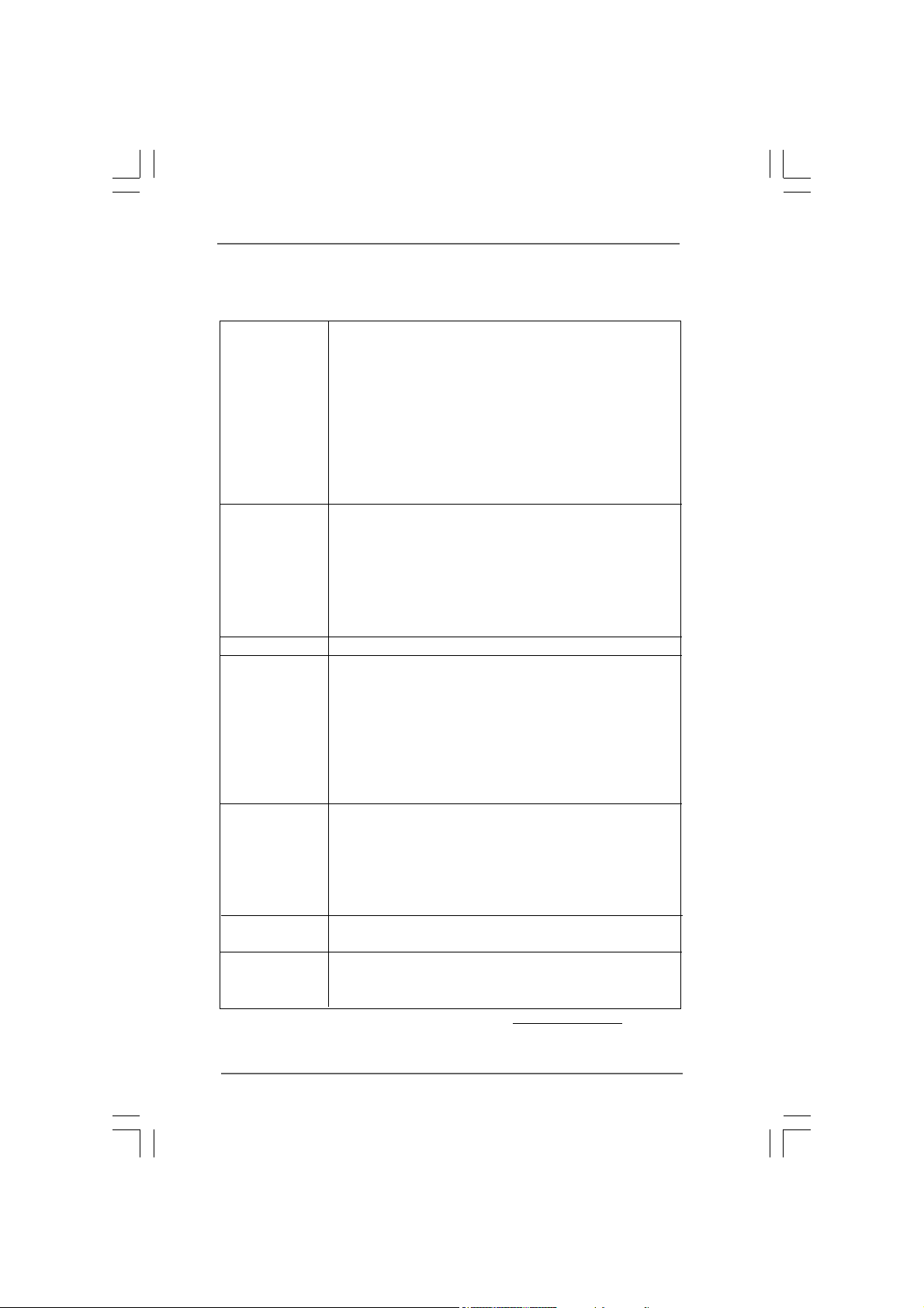
Connector - 2 x SATAII 3.0 Gb/s connectors (No Support for RAID and
“Hot Plug” functions) (see CAUTION 7)
- 1 x ATA100 IDE connector (supports 2 x IDE devices)
- 1 x Print port header
- CPU/Chassis FAN connector
- 24 pin ATX power connector
- 4 pin 12V power connector
- Front panel audio connector
- 2 x USB 2.0 headers (support 4 USB 2.0 ports)
(see CAUTION 8)
BIOS Feature - 8Mb AMI BIOS
- AMI Legal BIOS
- Supports “Plug and Play”
- ACPI 1.1 Compliance Wake Up Events
- SMBIOS 2.3.1 Support
- VCCM, NB, VTT Voltage Multi-adjustment
- Supports Smart BIOS
Support CD - Drivers, Utilities, AntiVirus Software (Trial Version)
Unique Feature - ASRock OC Tuner (see CAUTION 9)
- Intelligent Energy Saver (see CAUTION 10)
- Instant Boot
- ASRock Instant Flash (see CAUTION 11)
- Hybrid Booster:
- CPU Frequency Stepless Control (see CAUTION 12)
- ASRock U-COP (see CAUTION 13)
- Boot Failure Guard (B.F.G.)
Hardware - CPU Temperature Sensing
Monitor - Chassis Temperature Sensing
- CPU Fan Tachometer
- Chassis Fan Tachometer
- CPU Quiet Fan
- Voltage Monitoring: +12V, +5V, +3.3V, Vcore
OS - Microsoft
®
Windows® 2000 / XP / XP 64-bit / Vista
TM
/
VistaTM 64-bit / Win7 compliant
Certifications - FCC, CE
- EuP Ready (EuP ready power supply is required)
(see CAUTION 14)
* For detailed product information, please visit our website: http://www.asrock.com
77
7
77
Page 8

WA R NING
Please realize that there is a certain risk involved with overclocking, including adjusting
the setting in the BIOS, applying Untied Overclocking Technology, or using the third-
party overclocking tools. Overclocking may affect your system stability, or even
cause damage to the components and devices of your system. It should be done at
your own risk and expense. We are not responsible for possible damage caused by
overclocking.
CAUTION!
1. This motherboard supports CPU power up to 65W. Please refer to CPU
support list for compatible CPU. ASRock website:
2. About the setting of “Hyper Threading Technology”, please check page 36.
3. This motherboard supports Untied Overclocking Technology. Please read
“Untied Overclocking Technology” on page 24 for details.
4. This motherboard supports Dual Channel Memory Technology. Before you
implement Dual Channel Memory Technology, make sure to read the
installation guide of memory modules on page 16 for proper installation.
5. Due to the operating system limitation, the actual memory size may be
less than 4GB for the reservation for system usage under Windows® XP
®
and Windows
VistaTM. For Windows® XP 64-bit and Windows® VistaTM 64-
bit with 64-bit CPU, there is no such limitation.
6. The maximum shared memory size is defined by the chipset vendor and
is subject to change. Please check Intel
®
website for the latest information.
7. Before installing SATAII hard disk to SATAII connector, please read the “SATAII
Hard Disk Setup Guide” on page 23 to adjust your SATAII hard disk drive to
SATAII mode. You can also connect SATA hard disk to SATAII connector
directly.
8. Power Management for USB 2.0 works fine under Microsoft
VistaTM 64-bit / VistaTM / XP 64-bit / XP SP1 or SP2 / 2000 SP4.
9. It is a user-friendly ASRock overclocking tool which allows you to surveil
your system by hardware monitor function and overclock your hardware
devices to get the best system performance under Windows
environment. Please visit our website for the operation procedures of
ASRock OC Tuner. ASRock website:
http://www.asrock.com
10. Featuring an advanced proprietary hardware and software design,
Intelligent Energy Saver is a revolutionary technology that delivers
unparalleled power savings. In other words, it is able to provide excep-
tional power saving and improve power efficiency without sacrificing
computing performance. Please visit our website for the operation pro-
cedures of Intelligent Energy Saver.
ASRock website:
http://www.asrock.com
http://www.asrock.com
®
Windows
®
®
88
8
88
Page 9

11. ASRock Instant Flash is a BIOS flash utility embedded in Flash ROM.
This convenient BIOS update tool allows you to update system BIOS
without entering operating systems first like MS-DOS or Windows®. With
this utility, you can press <F6> key during the POST or press <F2> key to
BIOS setup menu to access ASRock Instant Flash. Just launch this tool
and save the new BIOS file to your USB flash drive, floppy disk or hard
drive, then you can update your BIOS only in a few clicks without prepar-
ing an additional floppy diskette or other complicated flash utility. Please
be noted that the USB flash drive or hard drive must use FAT32/16/12 file
system.
12. Although this motherboard offers stepless control, it is not recommended
to perform over-clocking. Frequencies other than the recommended CPU
bus frequencies may cause the instability of the system or damage the
CPU.
13. While CPU overheat is detected, the system will automatically shutdown.
Before you resume the system, please check if the CPU fan on the
motherboard functions properly and unplug the power cord, then plug it
back again. To improve heat dissipation, remember to spray thermal
grease between the CPU and the heatsink when you install the PC system.
14. EuP, stands for Energy Using Product, was a provision regulated by
European Union to define the power consumption for the completed system.
According to EuP, the total AC power of the completed system shall be
under 1.00W in off mode condition. To meet EuP standard, an EuP ready
motherboard and an EuP ready power supply are required. According to
Intel’s suggestion, the EuP ready power supply must meet the standard of
5v standby power efficiency is higher than 50% under 100 mA current
consumption. For EuP ready power supply selection, we recommend you
checking with the power supply manufacturer for more details.
99
9
99
Page 10
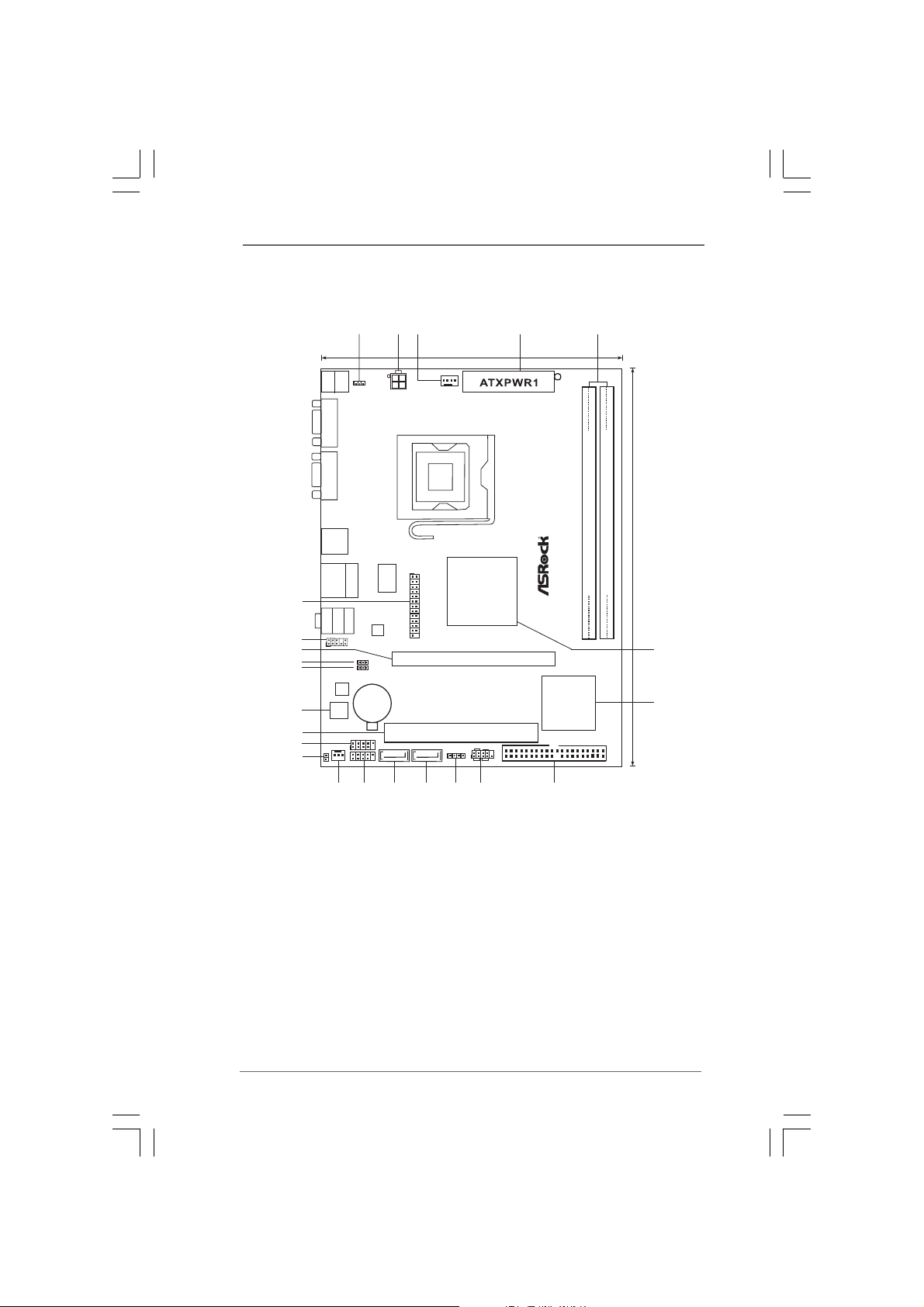
1.3 Motherboard Layout1.3 Motherboard Layout
1.3 Motherboard Layout
1.3 Motherboard Layout1.3 Motherboard Layout
3
24
1
5
17.0cm (6.7 in)
Keyboard
Mouse
PS2
PS2
1
PS2_USB_PWR1
ATX12V2
COM1
VGA1
USB 2.0
T:USB2
B: USB3
USB 2.0
T:USB0
B: USB1
23
Bottom:
MicIn
HD_AUDIO1
22
1
21
20
19
8Mb
18
BIOS
17
16
CHA_FAN1
15
CLRCMOS1
Super
Top:
IO
RJ-45
LineOut
Center:
LineIn
Top:
LAN
PHY
EUP_LAN
1
1
EUP_AUDIO1
AUDIO
CODEC
CMOS
Battery
USB6_7
SATAII_1
1
1
USB4_5
1
LPT1
RoHS
SATAII_2
CPU_FAN1
Intel
G41
Chipset
EuP Ready
PCIE1
PCI1
PANEL1
PLED PWRBTN
SPEAKER1
1
1
HDLED RESET
DX10
FSB1333
DDR2 800
G41M-VS
Intel
ICH7
IDE1
Dual Channel
FSB800
DDRII_1 (64bit, 240-pin module)
FSB800
DDRII_2 (64bit, 240-pin module)
22.4cm (8.8 in)
6
7
14
13
11
12
910
8
1 PS2_USB_PWR1 Jumper 12 Primary SAT AII Connector (SA T AII_1; Red)
2 ATX 12V Connector (A TX12V2) 13 USB 2.0 Header (USB4_5, Blue)
3 CPU Fan Connector (CPU_FAN1) 14 Chassis Fan Connector (CHA_FAN1)
4 A TX Power Connector (ATXPWR1) 1 5 Clear CMOS Jumper (CLRCMOS1)
5 2 x 240-pin DDR2 DIMM Slots 16 USB 2.0 Header (USB6_7, Blue)
(Dual Channel: DDRII_1, DDRII_2; Yellow) 17 PCI Slot (PCI1)
6 North Bridge Controller 18 BIOS SPI Chip
7 South Bridge Controller 19 EUP Audio Jumper (EUP_AUDIO1)
8 IDE1 Connector (IDE1, Blue) 20 EUP LAN Jumper (EUP_LAN1)
9 System Panel Hea der (P ANEL1, Orange) 21 PCI Express x16 Slot (PCIE1)
10 Chassis Speaker Header 22 Front Panel Audio Header
(SPEAKER 1, Purple) (HD_AUDIO1, Lime)
11 Secondary SAT AII Conne ctor (SA T AII_2; Red) 23 Print Port Header (LPT1, Purple)
1010
10
1010
Page 11
1.4 I/O P1.4 I/O P
1.4 I/O P
1.4 I/O P1.4 I/O P
anelanel
anel
anelanel
1
2
3
4
5
6
10
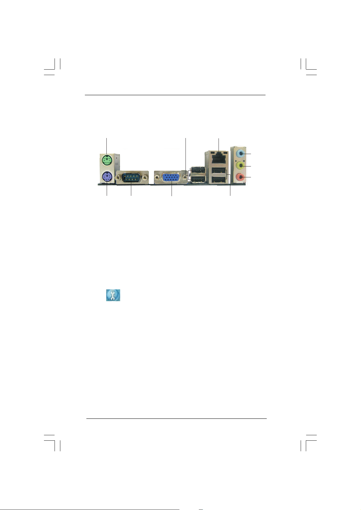
1 PS/2 Mouse Port (Green) 6 Microphone (Pink)
2 USB 2.0 Ports (USB23) 7 USB 2.0 Ports (USB01)
3 RJ-45 Port 8 VGA Port
4 Line In (Light Blue) 9 COM Port
5 Line Out (Lime) 10 PS/2 Keyboard Port (Purple)
* To enable Multi-Streaming function, you need to connect a front panel audio cable to the front
panel audio header. Please refer to below steps for the software setting of Multi-Streaming.
For Windows® XP:
After restarting your computer, you will find “Mixer” tool on your system. Please select “Mixer
ToolBox” , click “Enable playback multi-streaming”, and click “ok”. Choose “2CH” or
“4CH” and then you are allowed to select “Realtek HDA Primary output” to use Rear Speaker
and Front Speaker, or select “Realtek HDA Audio 2nd output” to use front panel audio. Then
reboot your system.
For Windows
After restarting your computer, please double-click “Realtek HD Audio Manager” on the
system tray. Set “Speaker Configuration” to “Quadraphonic” or “Stereo”. Click “Device
advanced settings”, choose “Make front and rear output devices playbacks two different audio
streams simultaneously”, and click “ok”. Then reboot your system.
®
VistaTM:
9
8
7
1111
11
1111
Page 12
Chapter 2 InstallationChapter 2 Installation
Chapter 2 Installation
Chapter 2 InstallationChapter 2 Installation
G41M-VS is a Micro ATX form factor (8.8" x 6.7", 22.4 x 17.0 cm) motherboard.
Before you install the motherboard, study the configuration of your chassis to en-
sure that the motherboard fits into it.
Make sure to unplug the power cord before installing or removing the
motherboard. Failure to do so may cause physical injuries to you and
damages to motherboard components.
2.1 Screw Holes2.1 Screw Holes
2.1 Screw Holes
2.1 Screw Holes2.1 Screw Holes
Place screws into the holes indicated by circles to secure the motherboard to the
chassis.
Do not over-tighten the screws! Doing so may damage the motherboard.
2.2 Pre-installation Precautions2.2 Pre-installation Precautions
2.2 Pre-installation Precautions
2.2 Pre-installation Precautions2.2 Pre-installation Precautions
Take note of the following precautions before you install motherboard components
or change any motherboard settings.
1. Unplug the power cord from the wall socket before touching any component.
2. To avoid damaging the motherboard components due to static electricity, NEVER
place your motherboard directly on the carpet or the like. Also remember to use
a grounded wrist strap or touch a safety grounded object before you handle
components.
3. Hold components by the edges and do not touch the ICs.
4. Whenever you uninstall any component, place it on a grounded antistatic pad or
in the bag that comes with the component.
1212
12
1212
Before you install or remove any component, ensure that the power is
switched off or the power cord is detached from the power supply.
Failure to do so may cause severe damage to the motherboard, peripherals,
and/or components.
Page 13
2.3 CPU Installation2.3 CPU Installation
2.3 CPU Installation
2.3 CPU Installation2.3 CPU Installation
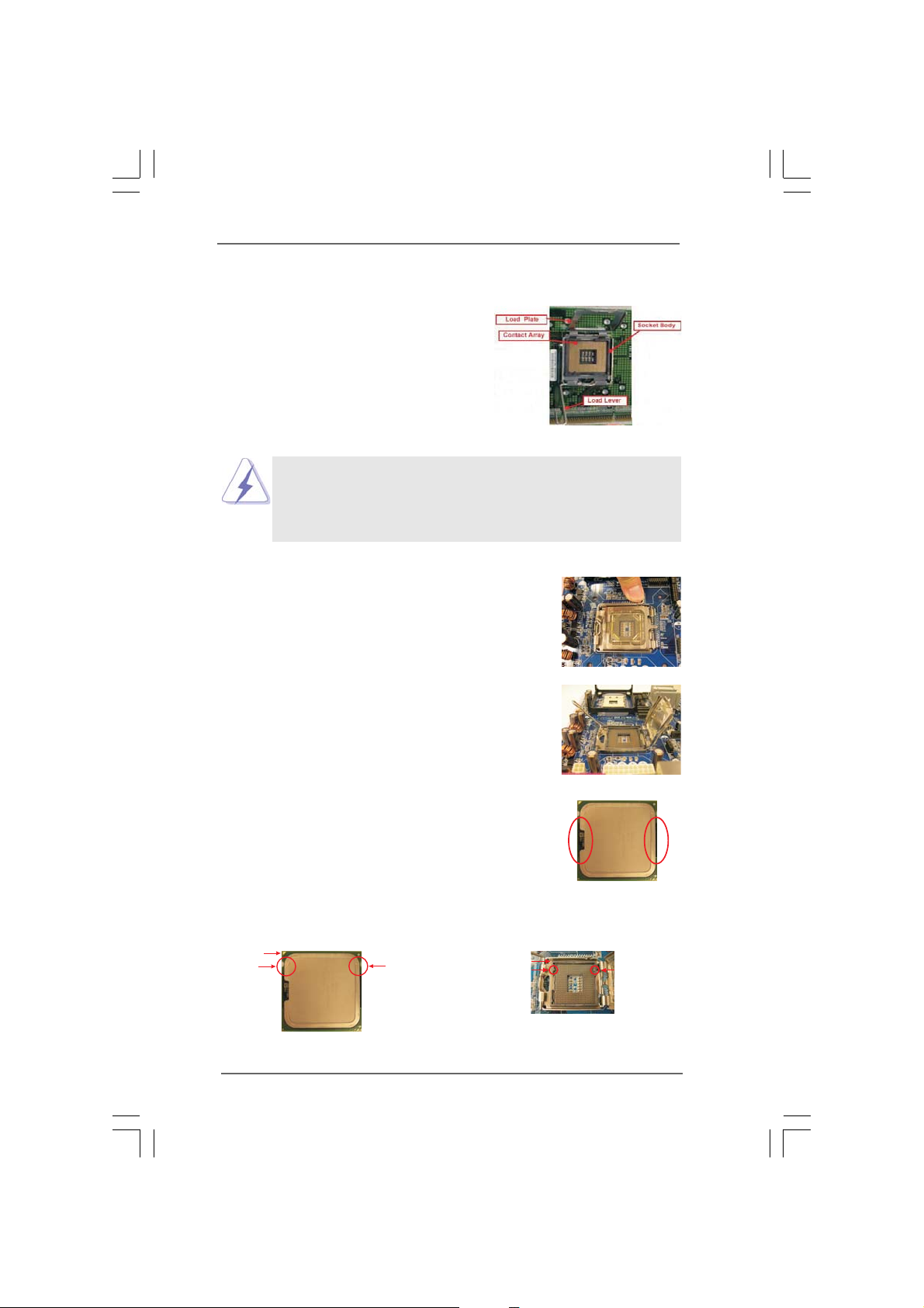
For the installation of Intel 775-LAND CPU,
please follow the steps below.
Before you insert the 775-LAND CPU into the socket, please check if
the CPU surface is unclean or if there is any bent pin on the socket.
Do not force to insert the CPU into the socket if above situation is
found. Otherwise, the CPU will be seriously damaged.
775-Pin Socket Overview
Step 1. Open the socket:
Step 1-1. Disengaging the lever by depressing
Lift Lever Up to 90°
down and out on the hook to clear
retention tab.
Step 1-2. Rotate the load lever to fully open po-
sition at approximately 135 degrees.
Step 1-3. Rotate the load plate to fully open po-
sition at approximately 100 degrees.
Step 2. Insert the 775-LAND CPU:
Step 2-1. Hold the CPU by the edges where are
marked with black lines.
Step 2-2. Orient the CPU with IHS (Integrated
Heat Sink) up. Locate Pin1 and the two
orientation key notches.
Pin1
orientation
key notch
orientation
key notch
CPU Marked Corner
Socket Marked Corner
alignment key
Pin1
black line
black line
alignment key
775-LAND CPU
775-Pin Socket
1313
13
1313
Page 14
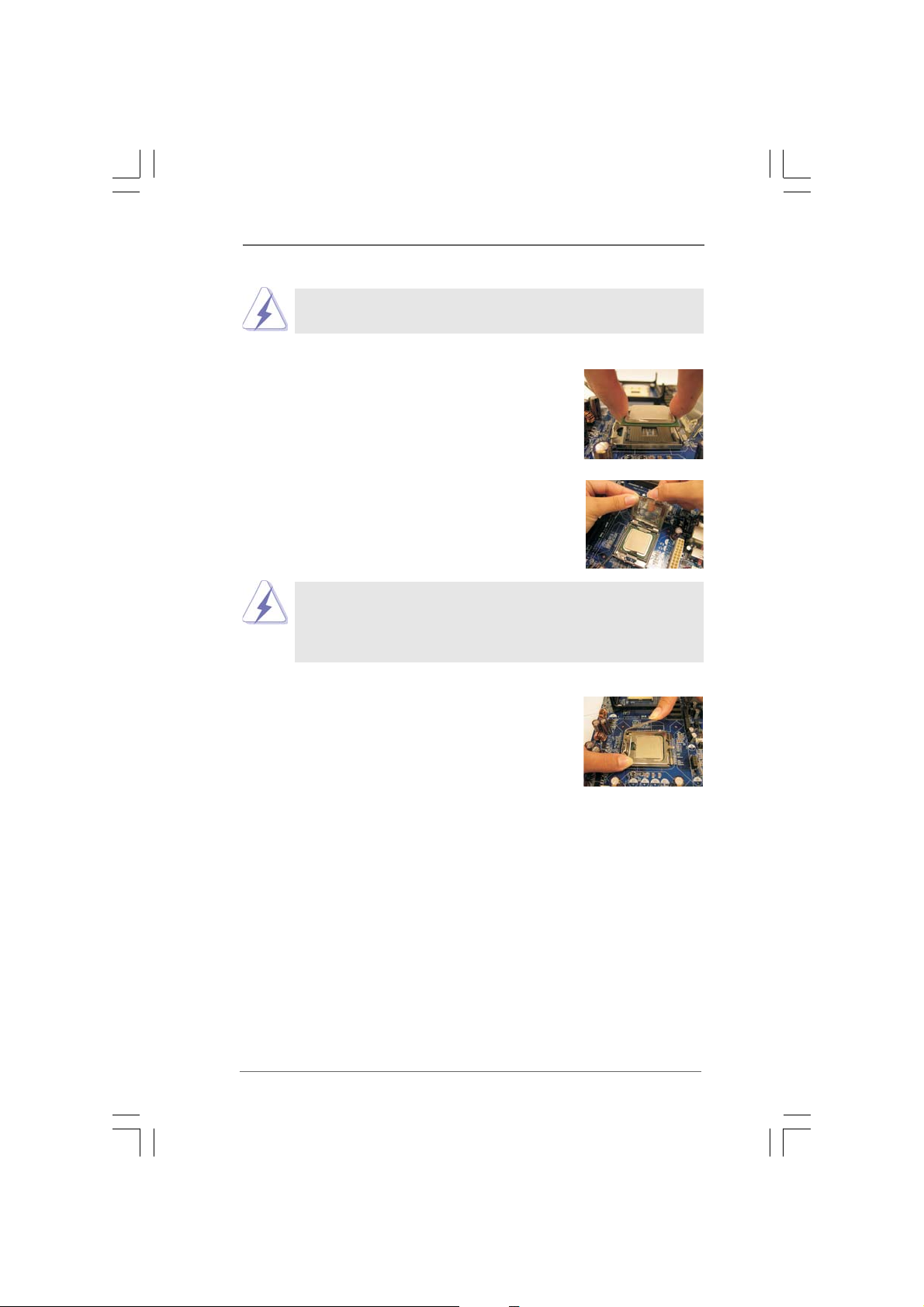
For proper inserting, please ensure to match the two orientation key
notches of the CPU with the two alignment keys of the socket.
Step 2-3. Carefully place the CPU into the socket
by using a purely vertical motion.
Step 2-4. Verify that the CPU is within the socket
and properly mated to the orient keys.
Step 3. Remove PnP Cap (Pick and Place Cap):
Use your left hand index finger and thumb to
support the load plate edge, engage PnP cap
with right hand thumb and peel the cap from the
socket while pressing on center of PnP cap to
assist in removal.
1. It is recommended to use the cap tab to handle and avoid kicking
off the PnP cap.
2. This cap must be placed if returning the motherboard for after
service.
Step 4. Close the socket:
Step 4-1. Rotate the load plate onto the IHS.
Step 4-2. While pressing down lightly on load
plate, engage the load lever.
Step 4-3. Secure load lever with load plate tab
under retention tab of load lever.
1414
14
1414
Page 15
2.42.4
Installation of CPU Fan and HeatsinkInstallation of CPU Fan and Heatsink
2.4
Installation of CPU Fan and Heatsink
2.42.4
Installation of CPU Fan and HeatsinkInstallation of CPU Fan and Heatsink
This motherboard is equipped with 775-Pin socket that supports Intel 775-LAND CPU.
Please adopt the type of heatsink and cooling fan compliant with Intel 775-LAND CPU
to dissipate heat. Before you installed the heatsink, you need to spray thermal
interface material between the CPU and the heatsink to improve heat dissipation.
Ensure that the CPU and the heatsink are securely fastened and in good contact with
each other. Then connect the CPU fan to the CPU_FAN connector (CPU_FAN1, see
page 10, No. 3).
For proper installation, please kindly refer to the instruction manuals of
your CPU fan and heatsink.
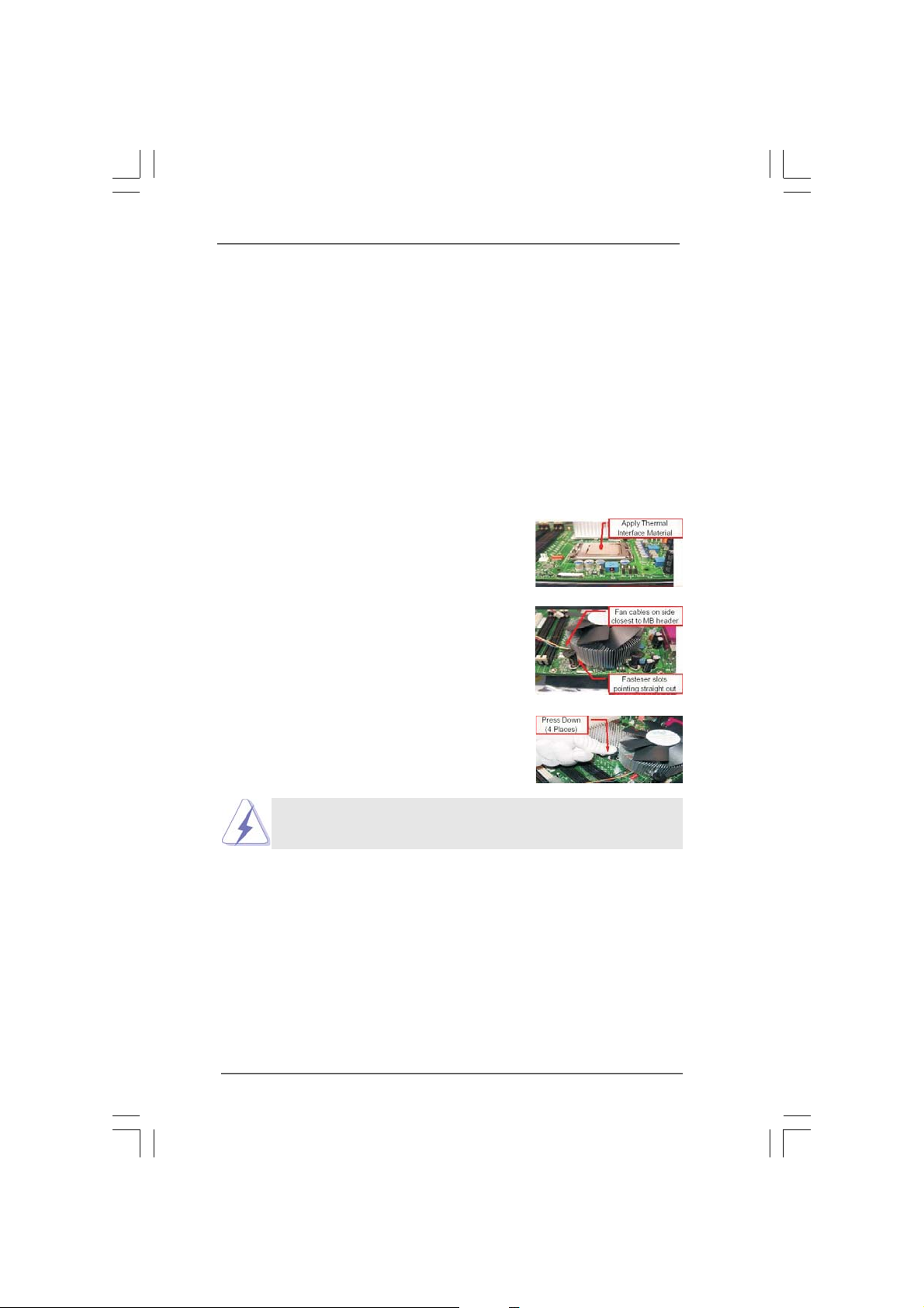
Below is an example to illustrate the installation of the heatsink for 775-LAND CPU.
Step 1. Apply thermal interface material onto center
of IHS on the socket surface.
Step 2. Place the heatsink onto the socket. Ensure
fan cables are oriented on side closest to the
CPU fan connector on the motherboard
(CPU_FAN1, see page 10, No. 3).
Step 3. Align fasteners with the motherboard
throughholes.
Step 4. Rotate the fastener clockwise, then press
down on fastener caps with thumb to install
and lock. Repeat with remaining fasteners.
If you press down the fasteners without rotating them clockwise,
the heatsink cannot be secured on the motherboard.
Step 5. Connect fan header with the CPU fan
connector on the motherboard.
Step 6. Secure excess cable with tie-wrap to ensure
cable does not interfere with fan operation or
contact other components.
1515
15
1515
Page 16
2.5 Installation of Memory Modules (DIMM)2.5 Installation of Memory Modules (DIMM)
2.5 Installation of Memory Modules (DIMM)
2.5 Installation of Memory Modules (DIMM)2.5 Installation of Memory Modules (DIMM)
G41M-VS motherboard provides two 240-pin DDR2 (Double Data Rate 2) DIMM
slots, and supports Dual Channel Memory Technology. For dual channel
configuration, you always need to install two identical (the same brand, speed,
size and chip-type) memory modules in the DDR2 DIMM slots to activate Dual
Channel Memory Technology. Otherwise, it will operate at single channel mode.
1. It is not allowed to install a DDR memory module into DDR2 slot;
otherwise, this motherboard and DIMM may be damaged.
2. If you install only one memory module or two non-identical memory
modules, it is unable to activate the Dual Channel Memory Technology.
Installing a DIMMInstalling a DIMM
Installing a DIMM
Installing a DIMMInstalling a DIMM
Please make sure to disconnect power supply before adding or
removing DIMMs or the system components.
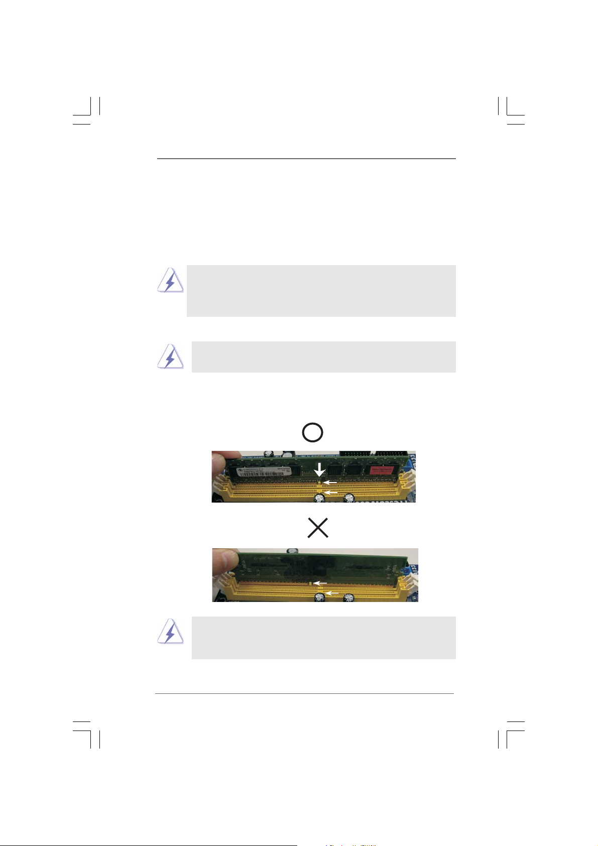
Step 1. Unlock a DIMM slot by pressing the retaining clips outward.
Step 2. Align a DIMM on the slot such that the notch on the DIMM matches the break
on the slot.
notch
break
notch
break
The DIMM only fits in one correct orientation. It will cause permanent
damage to the motherboard and the DIMM if you force the DIMM into the
slot at incorrect orientation.
Step 3. Firmly insert the DIMM into the slot until the retaining clips at both ends fully
snap back in place and the DIMM is properly seated.
1616
16
1616
Page 17
2.6 Expansion Slots (PCI and PCI Express Slots)2.6 Expansion Slots (PCI and PCI Express Slots)
2.6 Expansion Slots (PCI and PCI Express Slots)
2.6 Expansion Slots (PCI and PCI Express Slots)2.6 Expansion Slots (PCI and PCI Express Slots)
There are 1 PCI slot and 1 PCI Express slot on this motherboard.
PCI slot: PCI slot is used to install expansion card that has the 32-bit PCI interface.
PCIE slot: PCIE1 (PCIE x16 slot) is used for PCI Express card with x16 lane width
graphics card.
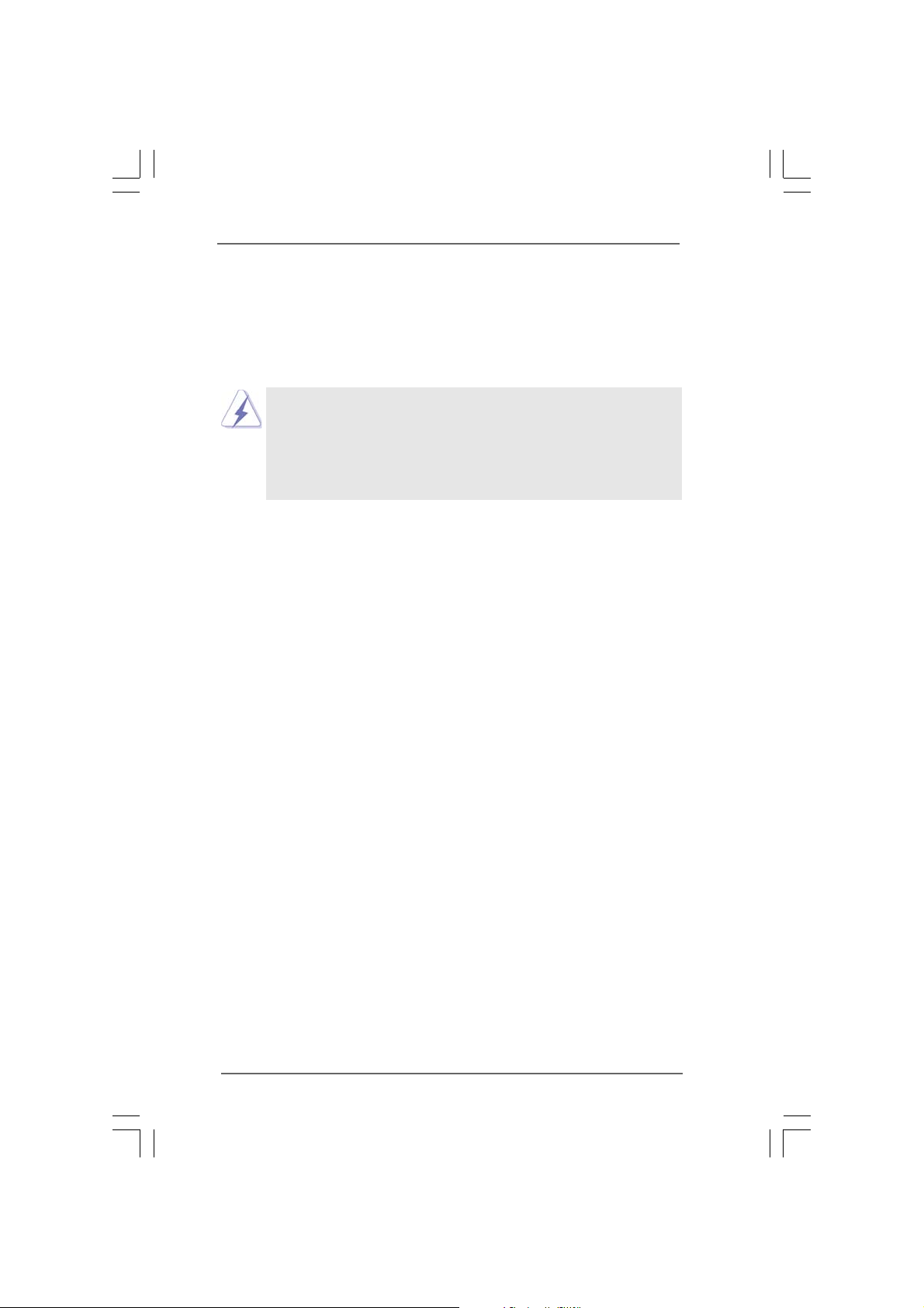
If you install the add-on PCI Express VGA card to PCIE1 (PCIE x16 slot),
the onboard VGA will be disabled. If you install the add-on PCI Express
VGA card to PCIE1 (PCIE x16 slot) and adjust the BIOS options “Primary
Graphics Adapter” to [Onboard] and “Share Memory” to [Auto], then the
onboard VGA will be enabled, and the primary screen will be onboard
VGA.
Installing an expansion cardInstalling an expansion card
Installing an expansion card
Installing an expansion cardInstalling an expansion card
Step 1. Before installing the expansion card, please make sure that the power
supply is switched off or the power cord is unplugged. Please read the
documentation of the expansion card and make necessary hardware
settings for the card before you start the installation.
Step 2. Remove the bracket facing the slot that you intend to use. Keep the screws
for later use.
Step 3. Align the card connector with the slot and press firmly until the card is
completely seated on the slot.
Step 4. Fasten the card to the chassis with screws.
1717
17
1717
Page 18
2.7 Jumpers Setup2.7 Jumpers Setup
2.7 Jumpers Setup
2.7 Jumpers Setup2.7 Jumpers Setup
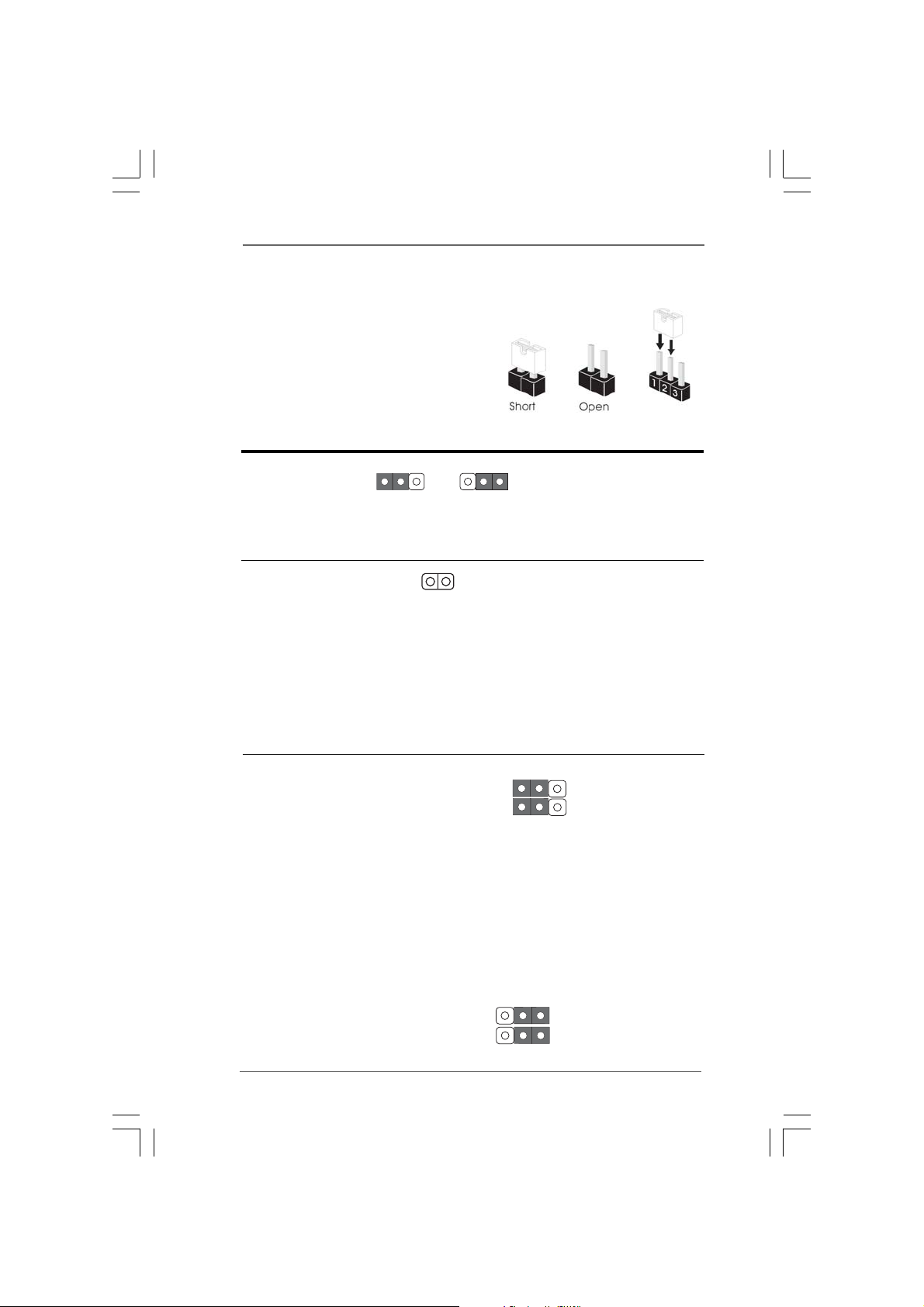
The illustration shows how jumpers are
setup. When the jumper cap is placed on
pins, the jumper is “Short”. If no jumper cap
is placed on pins, the jumper is “Open”. The
illustration shows a 3-pin jumper whose pin1
and pin2 are “Short” when jumper cap is
placed on these 2 pins.
Jumper Setting Description
PS2_USB_PWR1 Short pin2, pin3 to enable
(see p.10 No. 1) +5VSB (standby) for PS/2
1_2
+5V
2_3
+5VSB
or USB wake up events.
Note: To select +5VSB, it requires 2 Amp and higher standby current provided by
power supply.
Clear CMOS
(CLRCMOS1, 2-pin jumper)
(see p.10 No. 15)
2-pin jumper
Note: CLRCMOS1 allows you to clear the data in CMOS. The data in CMOS includes
system setup information such as system password, date, time, and system
setup parameters. To clear and reset the system parameters to default setup,
please turn off the computer and unplug the power cord from the power
supply. After waiting for 15 seconds, use a jumper cap to short 2 pins on
CLRCMOS1 for 5 seconds.
EUP LAN / EUP Audio Jumper
(EUP_LAN1, 3-pin jumper, see p.10 No. 20)
(EUP_AUDIO1, 3-pin jumper, see p.10 No. 19)
EUP_LAN1
EUP_AUDIO1
Default (Enable EuP)
Note: EUP_LAN and EUP_AUDIO jumper design decreases the power consumption
of this motherboard to meet EuP standard. With an ASRock EuP ready
motherboard and a power supply that the 5VSB power efficiency is higher
than 50% under 100mA current consumption, your system is able to submit
EuP standard. The default setting (short pin1 and pin2) is EuP enabled. If you
want to disable this power saving function, you may short pin2 and pin3.
Please be noticed that when EUP_LAN jumper is set to enabled, the
Wake-On-LAN function under S3 (Suspend to RAM), S4 (Suspend to Disk),
and S5 (Soft Off) will be disabled.
1818
18
1818
EUP_LAN1
EUP_AUDIO1
(Disable EuP)
Page 19
2.8 Onboard Headers and Connectors2.8 Onboard Headers and Connectors
2.8 Onboard Headers and Connectors
2.8 Onboard Headers and Connectors2.8 Onboard Headers and Connectors
Onboard headers and connectors are NOT jumpers. Do NOT place
jumper caps over these headers and connectors. Placing jumper caps
over the headers and connectors will cause permanent damage of the
motherboard!
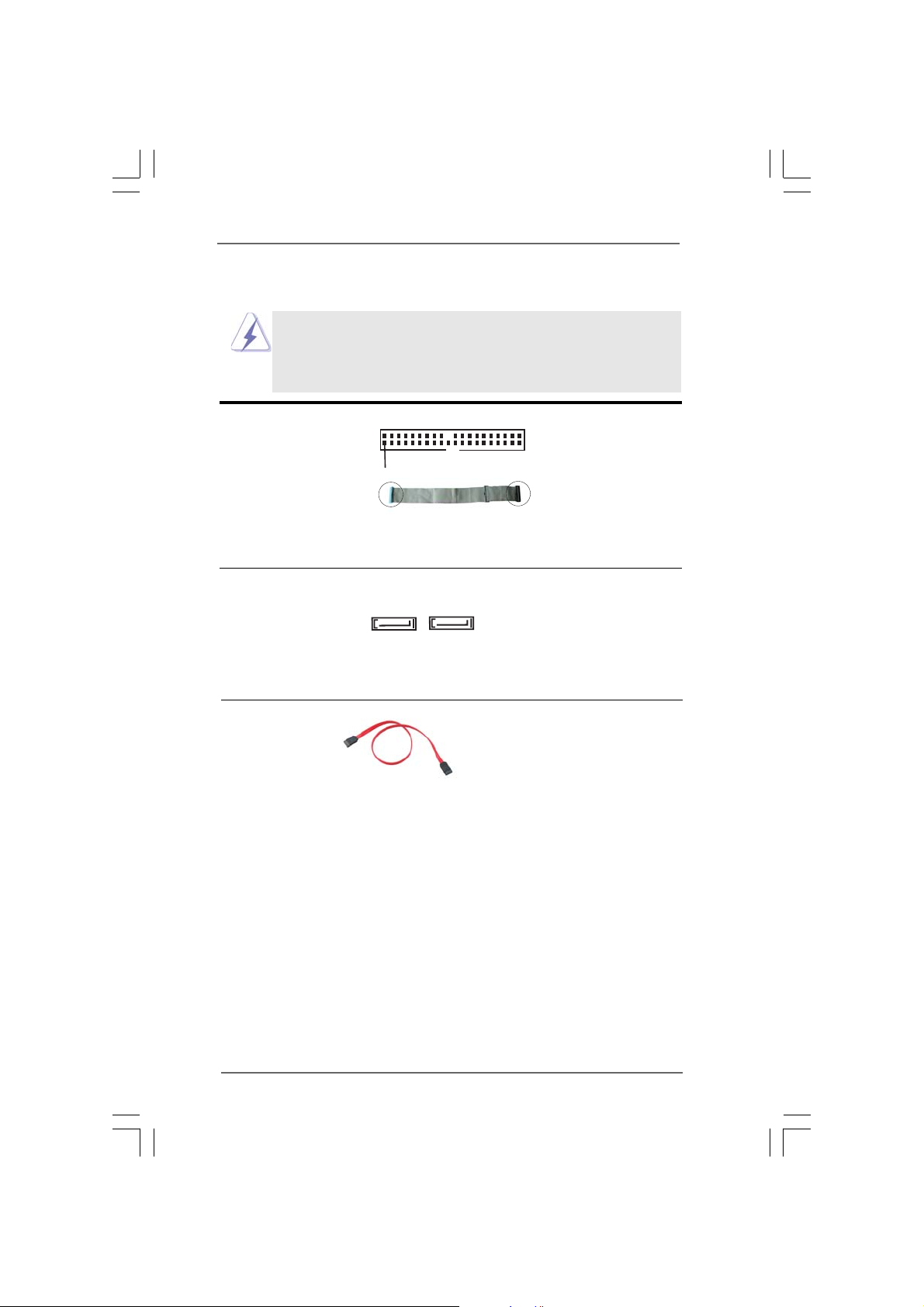
Primary IDE connector (Blue)
(39-pin IDE1, see p.10 No. 8)
PIN1
connect the blue end
to the motherboard
IDE1
connect the black end
to the IDE devices
80-conductor ATA 66/100 cable
Note: Please refer to the instruction of your IDE device vendor for the details.
Serial ATAII Connectors These Serial ATAII (SATAII)
(SATAII_1: see p.10, No. 12) connectors support SATAII
(SATAII_2: see p.10, No. 11) or SATA hard disk for internal
SATAII_1 SATAII_2
storage devices. The current
SATAII interface allows up to
3.0 Gb/s data transfer rate.
Serial ATA (SATA) Either end of the SATA data cable
Data Cable can be connected to the SATA /
(Optional) SATAII hard disk or the SATAII
connector on the motherboard.
1919
19
1919
Page 20
1
1
USB_PWR
P-7
P-6
USB_PWR
USB_PWR
P-5
P-4
USB_PWR
P+7
P+6
P+5
P+4
GND
GND
GND
GND
DUMMY
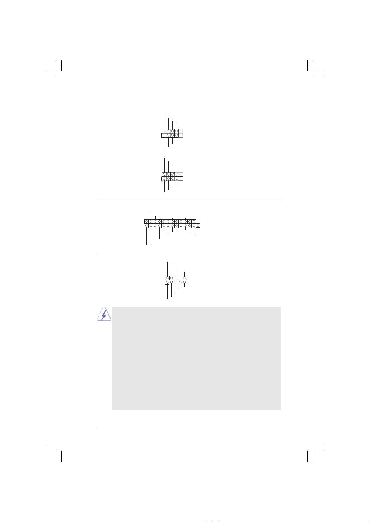
motherboard. Each USB 2.0
header can support two USB
2.0 ports.
DUMMY
USB 2.0 Headers Besides four default USB 2.0
(9-pin USB6_7) ports on the I/O panel, there are
(see p.10 No. 16) two USB 2.0 headers on this
(9-pin USB4_5)
(see p.10 No. 13)
Print Port Header This is an interface for print
(25-pin LPT1) port cable that allows
(see p.10 No. 23) convenient connection of printer
Front Panel Audio Header This is an interface for front
(9-pin HD_AUDIO1) panel audio cable that allows
(see p.10 No. 22) convenient connection and
1
AFD#
STB#
ERROR#
PINIT#
SPD1
SPD0
SLIN#
SPD2
SPD3
1
SPD4
GND
MIC2_L
GND
SPD6
SPD5
PRE SENCE#
MIC_RET
OUT2_R
MIC2_R
SPD7
ACK#
J_SENSE
BUSY
OUT_R ET
OUT2_L
devices.
PE
SLCT
control of audio devices.
1. High Definition Audio supports Jack Sensing, but the panel wire on
the chassis must support HDA to function correctly. Please follow the
instruction in our manual and chassis manual to install your system.
2. If you use AC’97 audio panel, please install it to the front panel audio
header as below:
A. Connect Mic_IN (MIC) to MIC2_L.
B. Connect Audio_R (RIN) to OUT2_R and Audio_L (LIN) to OUT2_L.
C. Connect Ground (GND) to Ground (GND).
D. MIC_RET and OUT_RET are for HD audio panel only. You don’t
need to connect them for AC’97 audio panel.
E. Enter BIOS Setup Utility. Enter Advanced Settings, and then select
Chipset Configuration. Set the Front Panel Control option from
[Auto] to [Enabled].
F. Enter Windows system. Click the icon on the lower right hand
taskbar to enter Realtek HD Audio Manager.
2020
20
2020
Page 21
For Windows® 2000 / XP / XP 64-bit OS:
Click “Audio I/O”, select “Connector Settings” , choose
“Disable front panel jack detection”, and save the change by
clicking “OK”.
For Windows
®
VistaTM / VistaTM 64-bit OS:
Click the right-top “Folder” icon , choose “Disable front
panel jack detection”, and save the change by clicking “OK”.
G. To activate the front mic.
®
For Windows
2000 / XP / XP 64-bit OS:
Please select “Front Mic” as default record device.
If you want to hear your voice through front mic, please deselect "Mute"
icon in “Front Mic” of “Playback” portion.
For Windows® VistaTM / VistaTM 64-bit OS:
Go to the "Front Mic" Tab in the Realtek Control panel.
Click "Set Default Device" to make the Front Mic as the default record
device.
1
1
PLED+
PLED-
HDLED -
HDLED +
DUMMY
+5V
PWRBTN#
GND
DUMMY
RES ET#
GND
SPEAKER
DUMMY
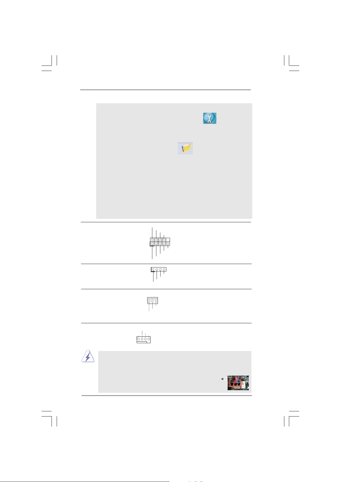
System Panel Header This header accommodates
(9-pin PANEL1) several system front panel
(see p.10 No. 9) functions.
Chassis Speaker Header Please connect the chassis
(4-pin SPEAKER 1) speaker to this header.
(see p.10 No. 10)
Chassis Fan Connector Please connect a chassis fan
(3-pin CHA_FAN1) cable to this connector and
(see p.10 No. 14) match the black wire to the
CPU Fan Connector Please connect a CPU fan cable
(4-pin CPU_FAN1) to this connector and match
(see p.10 No. 3) the black wire to the ground pin.
+12V
GND
1 2 3 4
Though this motherboard provides 4-Pin CPU fan (Quiet Fan) support, the 3-Pin
CPU fan still can work successfully even without the fan speed control function.
If you plan to connect the 3-Pin CPU fan to the CPU fan connector on this
motherboard, please connect it to Pin 1-3.
GND
+12V
CHA_FAN_SPEED
CPU_FAN_SPEED
FAN_S PEED_CONTROL
ground pin.
Pin 1-3 Connected
3-Pin Fan Installation
2121
21
2121
Page 22
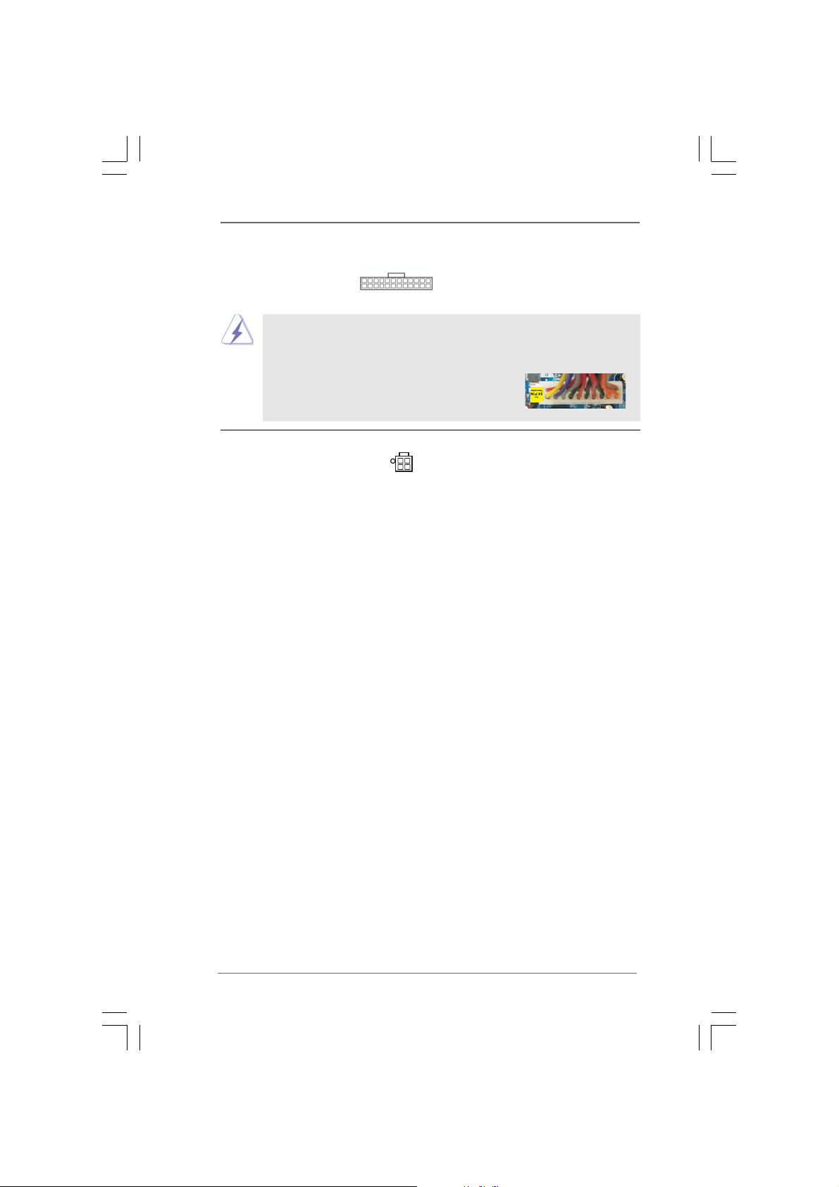
ATX Power Connector Please connect an ATX power
(24-pin ATXPWR1) supply to this connector.
(see p.10 No. 4)
24 13
12 1
Though this motherboard provides 24-pin ATX power connector, it can still work
if you adopt a traditional 20-pin ATX power supply. To use the 20-pin ATX power
supply, please plug your power supply along with Pin 1 and Pin 13.
24 13
20-Pin ATX Power Supply Installation
12 1
ATX 12V Connector Please note that it is necessary
(4-pin ATX12V2) to connect a power supply with
(see p.10 No. 2) ATX 12V plug to this connector
so that it can provides sufficient
power. Failing to do so will cause
the failure to power up.
2222
22
2222
Page 23
2.92.9
SASA
TT
2.9
2.92.9
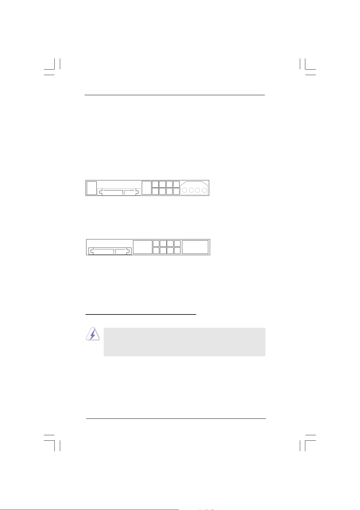
Before installing SATAII hard disk to your computer, please carefully read below
SATAII hard disk setup guide. Some default setting of SATAII hard disks may not
be at SATAII mode, which operate with the best performance. In order to enable
SATAII function, please follow the below instruction with different vendors to
correctly adjust your SATAII hard disk to SATAII mode in advance; otherwise, your
SATAII hard disk may fail to run at SATAII mode.
Western Digital
If pin 5 and pin 6 are shorted, SATA 1.5Gb/s will be enabled.
On the other hand, if you want to enable SATAII 3.0Gb/s, please remove the
jumpers from pin 5 and pin 6.
SAMSUNG
If pin 3 and pin 4 are shorted, SATA 1.5Gb/s will be enabled.
On the other hand, if you want to enable SATAII 3.0Gb/s, please remove the
jumpers from pin 3 and pin 4.
AII Hard Disk Setup GuideAII Hard Disk Setup Guide
SA
T
AII Hard Disk Setup Guide
SASA
TT
AII Hard Disk Setup GuideAII Hard Disk Setup Guide
1357
2468
1357
2468
HIT ACHI
Please use the Feature Tool, a DOS-bootable tool, for changing various ATA
features. Please visit HITACHI’s website for details:
http://www.hitachigst.com/hdd/support/download.htm
The above examples are just for your reference. For different SATAII hard
disk products of different vendors, the jumper pin setting methods may not
be the same. Please visit the vendors’ website for the updates.
2323
23
2323
Page 24

2.102.10
Serial ASerial A
2.10
Serial A
2.102.10
Serial ASerial A
Installation Installation
Installation
Installation Installation
This motherboard adopts Intel® ICH7 south bridge chipset that supports Serial ATA
(SATA) / Serial ATAII (SATAII) hard disks. You may install SATA / SATAII hard disks
on this motherboard for internal storage devices. This section will guide you to
install the SATA / SATAII hard disks.
STEP 1: Install the SATA / SATAII hard disks into the drive bays of your chassis.
STEP 2: Connect the SATA power cable to the SATA / SATAII hard disk.
STEP 3: Connect one end of the SATA data cable to the motherboard’s SATAII
connector.
STEP 4: Connect the other end of the SATA data cable to the SATA / SATAII hard
disk.
2.112.11
Driver Installation GuideDriver Installation Guide
2.11
Driver Installation Guide
2.112.11
Driver Installation GuideDriver Installation Guide
To install the drivers to your system, please insert the support CD to your optical drive
first. Then, the drivers compatible to your system can be auto-detected and listed on
the support CD driver page. Please follow the order from up to bottom side to install
those required drivers. Therefore, the drivers you install can work properly.
2.122.12
Untied Overclocking TUntied Overclocking T
2.12
Untied Overclocking T
2.122.12
Untied Overclocking TUntied Overclocking T
This motherboard supports Untied Overclocking Technology, which means during
overclocking, FSB enjoys better margin due to fixed PCI / PCIE buses. Before you
enable Untied Overclocking function, please enter “Overclock Mode” option of
BIOS setup to set the selection from [Auto] to [Manual]. Therefore, CPU FSB is
untied during overclocking, but PCI / PCIE buses are in the fixed mode so that FSB
can operate under a more stable overclocking environment.
TT
A (SAA (SA
T
A (SA
TT
A (SAA (SA
TT
A) / Serial AA) / Serial A
T
A) / Serial A
TT
A) / Serial AA) / Serial A
echnologyechnology
echnology
echnologyechnology
TT
AII (SAAII (SA
T
AII (SA
TT
AII (SAAII (SA
TT
AII) Hard DisksAII) Hard Disks
T
AII) Hard Disks
TT
AII) Hard DisksAII) Hard Disks
2424
24
2424
Please refer to the warning on page 8 for the possible overclocking risk
before you apply Untied Overclocking Technology.
Page 25

Chapter 3: BIOS SETUP UTILITYChapter 3: BIOS SETUP UTILITY
Chapter 3: BIOS SETUP UTILITY
Chapter 3: BIOS SETUP UTILITYChapter 3: BIOS SETUP UTILITY
3.1 Introduction3.1 Introduction
3.1 Introduction
3.1 Introduction3.1 Introduction
This section explains how to use the BIOS SETUP UTILITY to configure your system.
The SPI Memory on the motherboard stores the BIOS SETUP UTILITY. You may run the
BIOS SETUP UTILITY when you start up the computer. Please press <F2> or <Del>
during the Power-On-Self-Test (POST) to enter the BIOS SETUP UTILITY, otherwise,
POST will continue with its test routines.
If you wish to enter the BIOS SETUP UTILITY after POST, restart the system by press-
ing <Ctl> + <Alt> + <Delete>, or by pressing the reset button on the system chassis.
You may also restart by turning the system off and then back on.
Because the BIOS software is constantly being updated, the follow-
ing BIOS setup screens and descriptions are for reference purpose
only, and they may not exactly match what you see on your screen.
3.1.13.1.1
BIOS Menu BarBIOS Menu Bar
3.1.1
BIOS Menu Bar
3.1.13.1.1
BIOS Menu BarBIOS Menu Bar
The top of the screen has a menu bar with the following selections:
Main To set up the system time/date information
OC Tweaker To set up overclocking features
Advanced To set up the advanced BIOS features
H/W Monitor To display current hardware status
Boot To set up the default system device to locate and load the Op-
erating System
Security To set up the security features
Exit To exit the current screen or the BIOS SETUP UTILITY
Use < > key or < > key to choose among the selections on the menu bar,
and then press <Enter> to get into the sub screen.
2525
25
2525
Page 26
3.1.23.1.2
Navigation KeysNavigation Keys
3.1.2
Navigation Keys
3.1.23.1.2
Navigation KeysNavigation Keys
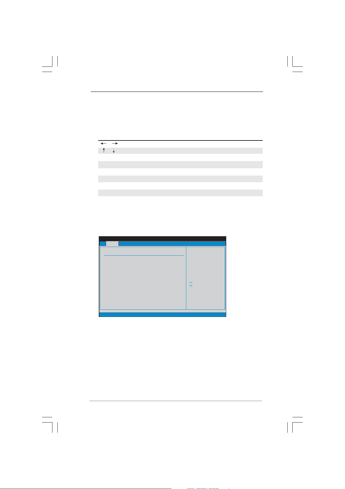
Please check the following table for the function description of each navigation
key.
Navigation Key(s) Function Description
/ Moves cursor left or right to select Screens
/ Moves cursor up or down to select items
+ / - To change option for the selected items
<Enter> To bring up the selected screen
<F1> To display the General Help Screen
<F9> To load optimal default values for all the settings
<F10> To save changes and exit the BIOS SETUP UTILITY
<ESC> To jump to the Exit Screen or exit the current screen
3.23.2
Main ScreenMain Screen
3.2
Main Screen
3.23.2
Main ScreenMain Screen
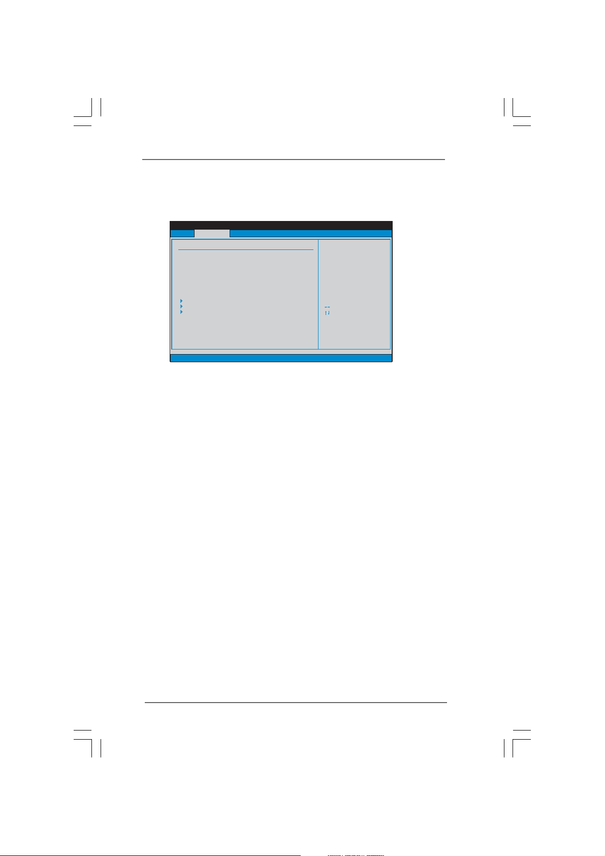
When you enter the BIOS SETUP UTILITY, the Main screen will appear and display
the system overview
OC Tweaker H/W Monitor Boot Security ExitAdvanced
Main
System Overview
System Time
System Date
BIOS Version
Processor Type
Processor Speed
Microcode Update
Cache Size
Total Memory
DDRII 1
DDRII 2
v02.54 (C)Copyright 1985-2005, American Megatrends, Inc.
BIOS SETUP UTILITY
: G41M-VS P1.00
:Intel(R)Core(TM)2DuoCPU
E6850 @ 3.00GHz (64bit)
: 3148MHz
: 6FB/B6
: 4096KB
: 2048MB with 256MB shared memory
and 2MB GTT memory
: 1024MB/420MHz (DDR2 840)
: 1024MB/420MHz (DDR2 840)
System Time [Hour:Minute:Second]
Use this item to specify the system time.
System Date [Day Month/Date/Year]
Use this item to specify the system date.
2626
26
2626
[ :00:09]
14
[Thu 08/06/2009]
Use [Enter], [TAB]
or [SHIFT-TAB] to
select a field.
Use [+] or [-] to
configure system Time.
Select Screen
Select Item
+- Change Field
Tab Select Field
F1 General Help
F9 Load Defaults
F10 Save and Exit
ESC Exit
Page 27
3.33.3
OC TOC T
weakweak
3.3
3.33.3
OC T
OC TOC T
weak
weakweak
er Screener Screen
er Screen
er Screener Screen
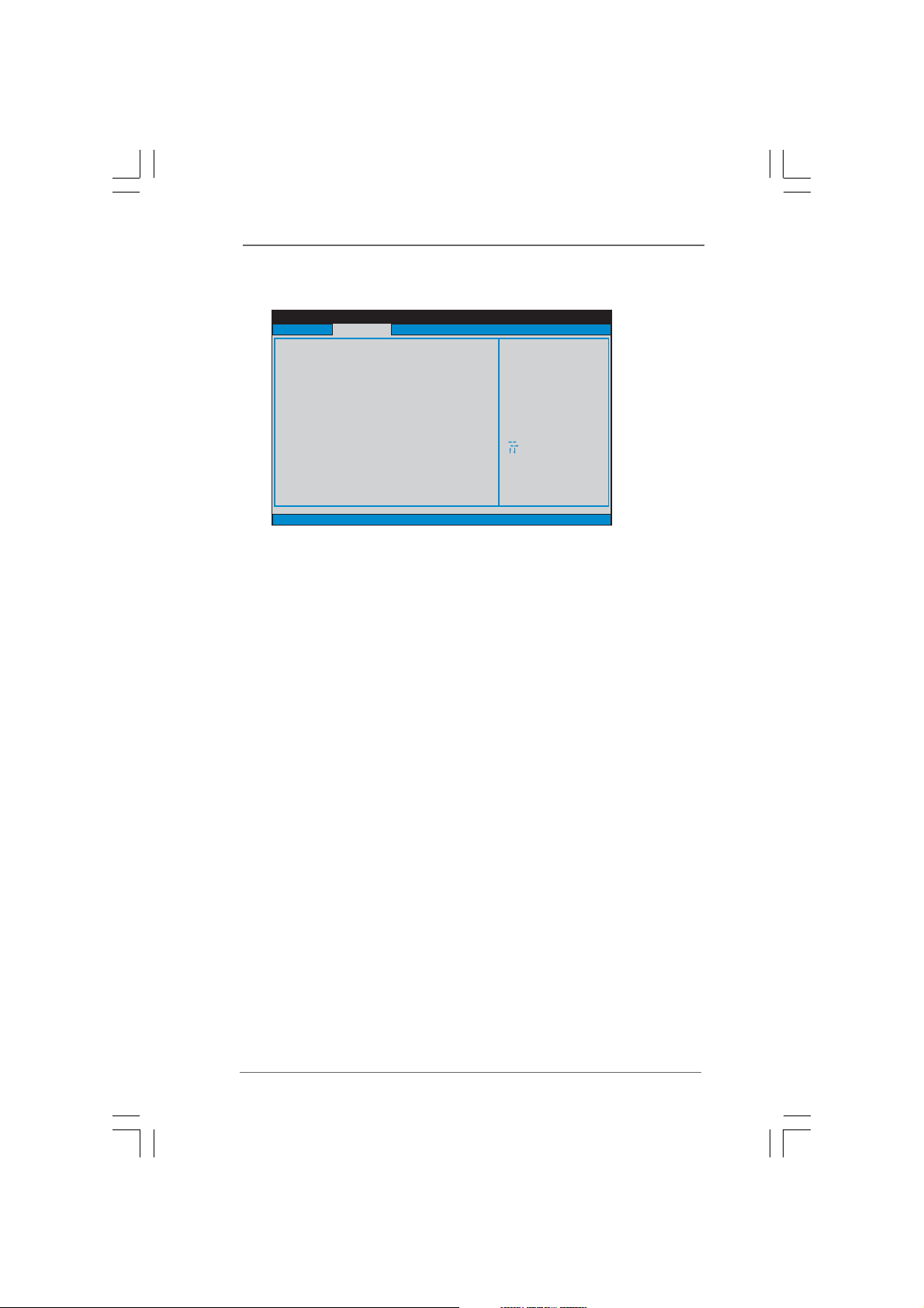
In the OC Tweaker screen, you can set up overclocking features.
Main
OC Tweaker
OC Tweaker Settings
Overclock Mode
CPU Frequency (MHz)
PCIE Frequency (MHz)
Boot Failure Guard
Spread Spectrum
Ratio Actual Value
DRAM Frequency
DRAM Timing Configuration
DRAM RCOMP STRENGTH Configuration
DRAM DLL SKEW Configuration
DRAM Voltage
NB Voltage
VTT Voltage
GTLRef Voltage
v02.54 (C)Copyright 1985-2005, American Megatrends, Inc.
BIOS SETUP UTILITY
Advanced H/W Monitor Boot Security Exit
Select the over clock
[Auto]
[350]
[103]
[Enabled]
[Auto]
9
[Auto]
[Auto]
[Auto]
[Auto]
[Auto]
mode.
Select Screen
Select Item
Enter Go to Sub Screen
F1 General Help
F9 Load Defaults
F10 Save and Exit
ESC Exit
Overclock Mode
Use this to select Overclock Mode. The default value is [Auto]. Configuration
options: [Auto], [Manual] and [Optimized].
CPU Frequency (MHz)
Use this option to adjust CPU frequency.
PCIE Frequency (MHz)
Use this option to adjust PCIE frequency.
Boot Failure Guard
Enable or disable the feature of Boot Failure Guard.
Spread Spectrum
This item should always be [Auto] for better system stability.
Ratio Actual Value
This is a read-only item, which displays the ratio actual value of this
motherboard.
DRAM Frequency
If [Auto] is selected, the motherboard will detect the memory module(s)
inserted and assigns appropriate frequency automatically. You may also
select other value as operating frequency: [333MHz (DDR2 667)] and
[400MHz (DDR2 800)].
2727
27
2727
Page 28
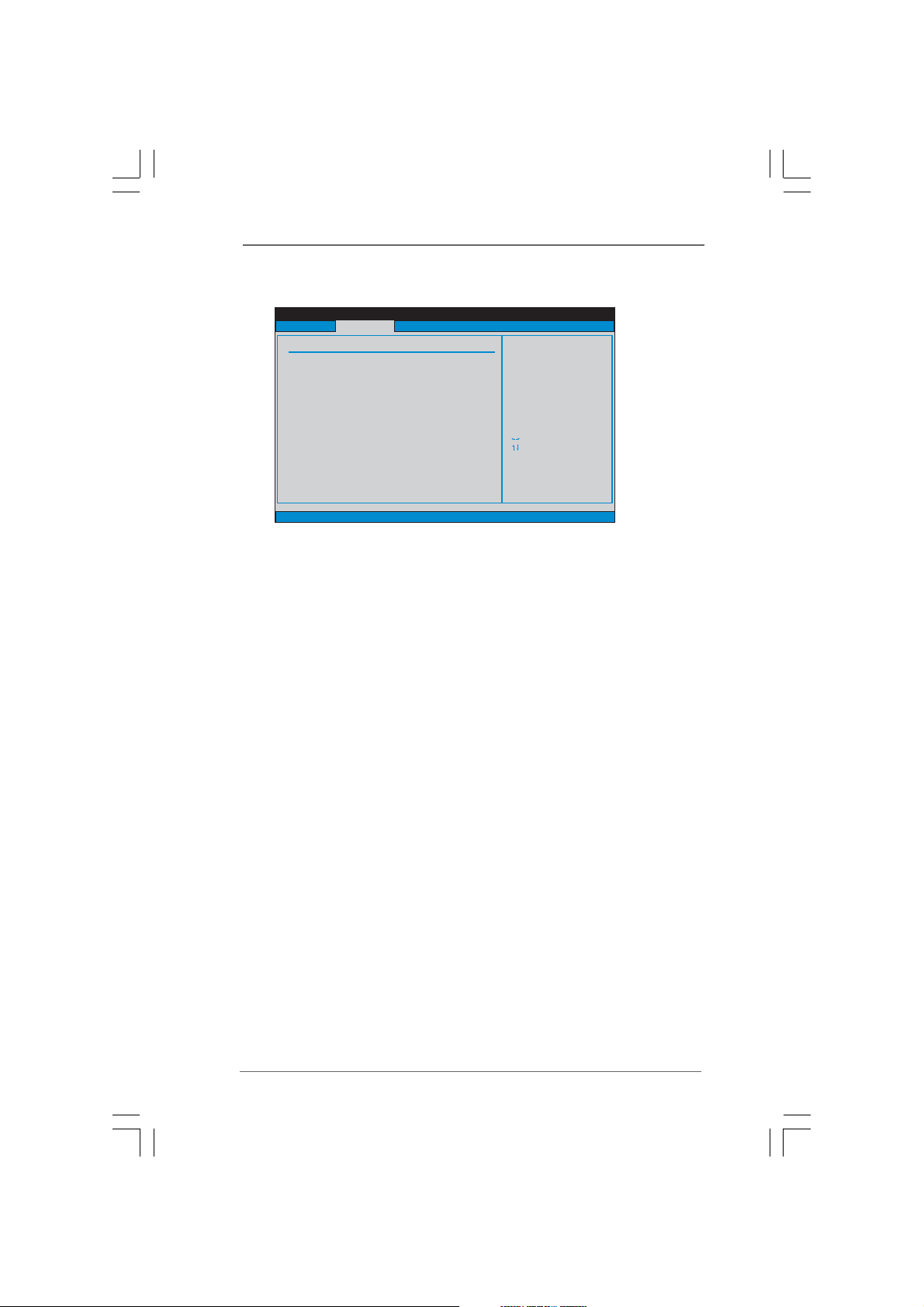
DRAM Timing Configuation
OC Tweaker
Standard Memory Info : 5-5-5-18-42-6-3-3-3
DRAM tCL
DRAM tRCD
DRAM tRP
DRAM tRAS
DRAM tRFC
DRAM tWR
DRAM tWTR
DRAM tRRD
DRAM tRTP
Advanced Memory Info : 18-18-7-7-0-0
DRAM CH0 RCOMP ODT
DRAM CH1 RCOMP ODT
DRAM CH0 tRD
DRAM CH1 tRD
DRAM CH0 tRD Phase Adjust
DRAM CH1 tRD Phase Adjust
v02.54 (C)Copyright 1985-2005, American Megatrends, Inc.
BIOS SETUP UTILITY
[Auto]
[Auto]
[Auto]
[Auto]
[Auto]
[Auto]
[Auto]
[Auto]
[Auto]
[Auto]
[Auto]
[Auto]
[Auto]
[Auto]
[Auto]
DRAM tCL
Val ue
Min=3
Max=7
Select Screen
Select Screen
Select Item
Select Item
+- Change Option
+- Change Option
F1 General Help
F1 General Help
F9 Load Defaults
F9 Load Defaults
F10 Save and Exit
F10 Save and Exit
ESC Exit
ESC Exit
DRAM tCL
This controls the number of DRAM clocks for TCL. Min: 3. Max: 7. The
default value is [Auto].
DRAM tRCD
This controls the number of DRAM clocks for TRCD. Min: 3. Max: 10. The
default value is [Auto].
DRAM tRP
This controls the number of DRAM clocks for TRP. Min: 3. Max: 10. The
default value is [Auto].
DRAM tRAS
This controls the number of DRAM clocks for TRAS. Min: 9. Max: 24. The
default value is [Auto].
DRAM tRFC
This controls the number of DRAM clocks for TRFC. Min: 15. Max: 78. The
default value is [Auto].
DRAM tWR
This controls the number of DRAM clocks for TWR. Min: 3. Max: 15. The
default value is [Auto].
DRAM tWTR
This controls the number of DRAM clocks for TWTR. Min: 2. Max: 15. The
default value is [Auto].
DRAM tRRD
This controls the number of DRAM clocks for TRRD. Min: 2. Max: 15. The
default value is [Auto].
DRAM tRTP
This controls the number of DRAM clocks for TRTP. Min: 2. Max: 13. The
default value is [Auto].
2828
28
2828
Page 29

DRAM CH0 RCOMP ODT
This controls the number of DRAM CH0 RCOMP ODT. Min: 1. Max: 63. The
default value is [Auto].
DRAM CH1 RCOMP ODT
This controls the number of DRAM CH1 RCOMP ODT. Min: 1. Max: 63. The
default value is [Auto].
DRAM CH0 tRD
This controls the number of DRAM CH0 TRD. Min: 0. Max: 30. The default
value is [Auto].
DRAM CH1 tRD
This controls the number of DRAM CH1 TRD. Min: 0. Max: 30. The default
value is [Auto].
DRAM CH0 tRD Phase Adjust
This controls the number of DRAM CH0 TR D Phase Adjust. M in: 0. M ax: 62.
The default value is [Auto].
DRAM CH1 tRD Phase Adjust
This controls the number of DRAM CH1 TR D Phase Adjust. M in: 0. M ax: 62.
The default value is [Auto].
2929
29
2929
Page 30
DRAM RCOMP STRENGTH Configuration
OC Tweaker
DRAM RCOMP STRENGTH Settings
DRAM CH0 RCOMP STRENGTH Info : 0-10-7-7-7-7
DRAM CH0 G0 (Data)
DRAM CH0 G1 (Command)
DRAM CH0 G2 (Control1)
DRAM CH0 G3 (Control2)
DRAM CH0 G4 (Clocks1)
DRAM CH0 G5 (Clocks2)
DRAM CH1 RCOMP STRENGTH Info : 0-10-7-0-7-0
DRAM CH1 G0 (Data)
DRAM CH1 G1 (Command)
DRAM CH1 G2 (Control1)
DRAM CH1 G3 (Control2)
DRAM CH1 G4 (Clocks1)
DRAM CH1 G5 (Clocks2)
v02.54 (C)Copyright 1985-2005, American Megatrends, Inc.
BIOS SETUP UTILITY
[Auto]
[Auto]
[Auto]
[Auto]
[Auto]
[Auto]
[Auto]
[Auto]
[Auto]
[Auto]
[Auto]
[Auto]
DRAM CH0 G0 (Data)
Val ue
Min=1
Max=15
Select Screen
Select Screen
Select Item
Select Item
+- Change Option
+- Change Option
F1 General Help
F1 General Help
F9 Load Defaults
F9 Load Defaults
F10 Save and Exit
F10 Save and Exit
ESC Exit
ESC Exit
DRAM CH0 G0 (Data)
This controls the number of DRAM CH0 G0 (Data). Min: 1. Max: 15. The
default value is [Auto].
DRAM CH0 G1 (Command)
This controls the number of DRAM CH0 G1 (Comma nd). Min: 1. Max: 15. The
default value is [Auto].
DRAM CH0 G2 (Control1)
This controls the number of DRAM CH0 G2 (Control1). Min: 1. Max: 15. The
default value is [Auto].
DRAM CH0 G3 (Control2)
This controls the number of DRAM CH0 G3 (Control2). Min: 1. Max: 15. The
default value is [Auto].
DRAM CH0 G4 (Clocks1)
This controls the number of D RAM CH0 G4 (Clocks1). Min: 1. Max: 15. The
default value is [Auto].
DRAM CH0 G5 (Clocks2)
This controls the number of D RAM CH0 G5 (Clocks2). Min: 1. Max: 15. The
default value is [Auto].
DRAM CH1 G0 (Data)
This controls the number of DRAM CH1 G0 (Data). Min: 1. Max: 15. The
default value is [Auto].
DRAM CH1 G1 (Command)
This controls the number of DRAM CH1 G1 (Comma nd). Min: 1. Max: 15. The
default value is [Auto].
DRAM CH1 G2 (Control1)
This controls the number of DRAM CH1 G2 (Control1). Min: 1. Max: 15. The
default value is [Auto].
3030
30
3030
Page 31

DRAM CH1 G3 (Control2)
This controls the number of DRAM CH1 G3 (Control2). Min: 1. Max: 15. The
default value is [Auto].
DRAM CH1 G4 (Clocks1)
This controls the number of DRAM CH1 G4 (Clocks1). Min: 1. Max: 15. The
default value is [Auto].
DRAM CH1 G5 (Clocks2)
This controls the number of DRAM CH1 G5 (Clocks2). Min: 1. Max: 15. The
default value is [Auto].
3131
31
3131
Page 32
DRAM DLL SKEW Settings
OC Tweaker
DRAM DLL SKEW Settings
DRAM CH0 CLKSET0 SKEW Info:11-5-1-0-0-1034
DRAM CH0 CLKSET0 SKEW
DRAM CH0 CLKSET1 SKEW Info:11-5-1-0-0-1034
DRAM CH0 CLKSET1 SKEW
DRAM CH0 CMD SKEW Info :3-4-1-1-0-311
DRAM CH0 CMD SKEW
DRAM CH0 CTRL0 SKEW Info :0-5-1-1-0-55
DRAM CH0 CTRL0 SKEW
DRAM CH0 CTRL1 SKEW Info :2-3-1-1-0-211
DRAM CH0 CTRL1 SKEW
DRAM CH0 CTRL2 SKEW Info :2-3-1-1-0-211
DRAM CH0 CTRL2 SKEW
DRAM CH0 CTRL3 SKEW Info :2-3-1-1-0-211
DRAM CH0 CTRL3 SKEW
DRAM CH1 CLKSET0 SKEW Info :11-5-1-0-0-1034
v02.54 (C)Copyright 1985-2005, American Megatrends, Inc.
BIOS SETUP UTILITY
[Auto]
[Auto]
[Auto]
[Auto]
[Auto]
[Auto]
[Auto]
Options
Auto
-350 ps
-300 ps
-250 ps
-200 ps
-150 ps
-100 ps
-50 ps
Normal
Select Screen
Select Screen
Select Item
Select Item
+- Change Option
+- Change Option
F1 General Help
F1 General Help
F9 Load Defaults
F9 Load Defaults
F10 Save and Exit
F10 Save and Exit
ESC Exit
ESC Exit
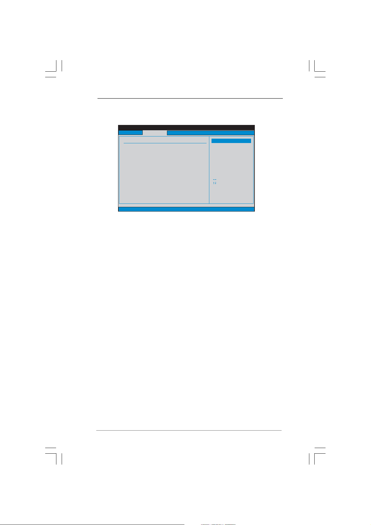
DRAM CH0 CLKSET0 SKEW
This controls the number of DRAM CH0 CLKSET0 SKEW. Configuration
options: [Auto], [Normal], [-350 ps] to [-50 ps]. The default value is [Auto].
DRAM CH0 CLKSET1 SKEW
This controls the number of DRAM CH0 CLKSET1 SKEW. Configuration
options: [Auto], [Normal], [-350 ps] to [-50 ps]. The default value is [Auto].
DRAM CH0 CMD SKEW
This controls the number of DRAM CH0 CMD SKEW. Conf iguration options :
[Auto], [Normal], [-350 ps] to [-50 ps]. The default value is [Auto].
DRAM CH0 CTRL0 SKEW
This controls the number of DRAM CH0 CTRL0 SKEW. Configuration options:
[Auto], [Normal], [-350 ps] to [-50 ps]. The default value is [Auto].
DRAM CH0 CTRL1 SKEW
This controls the number of DRAM CH0 CTRL1 SKEW. Configuration options:
[Auto], [Normal], [-350 ps] to [-50 ps]. The default value is [Auto].
DRAM CH0 CTRL2 SKEW
This controls the number of DRAM CH0 CTRL2 SKEW. Configuration options:
[Auto], [Normal], [-350 ps] to [-50 ps]. The default value is [Auto].
DRAM CH0 CTRL3 SKEW
This controls the number of DRAM CH0 CTRL3 SKEW. Configuration options:
[Auto], [Normal], [-350 ps] to [-50 ps]. The default value is [Auto].
DRAM CH1 CLKSET0 SKEW
This controls the number of DRAM CH1 CLKSET0 SKEW. Configuration
options: [Auto], [Normal], [-350 ps] to [-50 ps]. The default value is [Auto].
DRAM CH1 CLKSET1 SKEW
This controls the number of DRAM CH1 CLKSET1 SKEW. Configuration
options: [Auto], [Normal], [-350 ps] to [-50 ps]. The default value is [Auto].
3232
32
3232
Page 33

DRAM CH1 CMD SKEW
This controls the number of DRAM CH1 CMD SKEW. Conf iguration options :
[Auto], [Normal], [-350 ps] to [-50 ps]. The default value is [Auto].
DRAM CH1 CTRL0 SKEW
This controls the number of DRAM CH1 CTRL0 SKEW. Configuration options:
[Auto], [Normal], [-350 ps] to [-50 ps]. The default value is [Auto].
DRAM CH1 CTRL1 SKEW
This controls the number of DRAM CH1 CTRL1 SKEW. Configuration options:
[Auto], [Normal], [-350 ps] to [-50 ps]. The default value is [Auto].
DRAM CH1 CTRL2 SKEW
This controls the number of DRAM CH1 CTRL2 SKEW. Configuration options:
[Auto], [Normal], [-350 ps] to [-50 ps]. The default value is [Auto].
DRAM CH1 CTRL3 SKEW
This controls the number of DRAM CH1 CTRL3 SKEW. Configuration options:
[Auto], [Normal], [-350 ps] to [-50 ps]. The default value is [Auto].
3333
33
3333
Page 34

DRAM Voltage
Use this to select DRAM Voltage. Configuration options: [Auto], [1.794V] to
[2.201V]. The default value of this feature is [Auto].
NB Voltage
Use this to select NB Voltage. Configuration options: [Auto], [1.05V],
[1.11V], [1.23V] and [1.30V]. The default value of this feature is [Auto].
VTT Voltage
Use this to select VTT Voltage. Configuration options: [Auto], [1.10V],
[1.20V], [1.37V] and [1.46V]. The default value of this feature is [Auto].
GLTRef Voltage
Use this to select GLTRef Voltage. Configuration options: [Auto],
[0.67 x Vtt], [0.65 x Vtt], [0.63 x Vtt] and [0.615 x Vtt]. The default value of
this feature is [Auto].
Would you like to save current setting user defaults?
In this option, you are allowed to load and save three user defaults
according to your own requirements.
3434
34
3434
Page 35
3.43.4
Advanced ScreenAdvanced Screen
3.4
Advanced Screen
3.43.4
Advanced ScreenAdvanced Screen
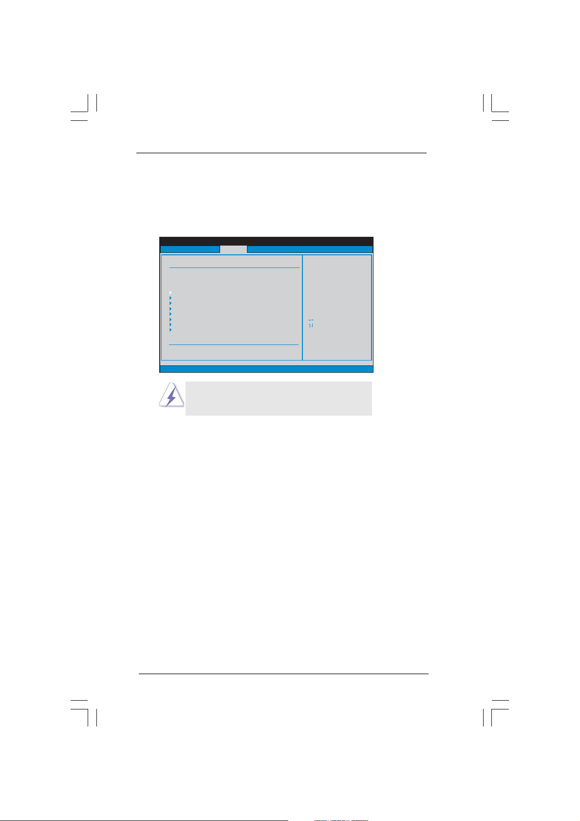
In this section, you may set the configurations for the following items: CPU
Configuration, Chipset Configuration, ACPI Configuration, Storage Configuration, PCIPnP
Configuration, SuperIO Configuration, and USB Configuration.
BIOS SETUP UTILITY
Main OC Tweaker
Advanced Settings
WARNING: Setting wrong values in below sections
BIOS Update Utility
ASRock Instant Flash
may cause system to malfunction.
CPU Configuration
Chipset Configuration
ACPI Configuration
Storage Configuration
PCIPnP Configuration
Floppy Configuration
SuperIO Configuration
USB Configuration
v02.54 (C)Copyright 1985-2005, American Megatrends, Inc.
H/W Monitor Boot Security Exit
Advanced
Options for CPU
Select Screen
Select Item
Enter Go to Sub Screen
F1 General Help
F9 Load Defaults
F10 Save and Exit
ESC Exit
Setting wrong values in this section may cause
the system to malfunction.
ASRock Instant Flash
ASRock Instant Flash is a BIOS flash utility embedded in Flash ROM. This
convenient BIOS update tool allows you to update system BIOS without
entering operating systems first like MS-DOS or Windows®. Just launch
this tool and save the new BIOS file to your USB flash drive, floppy disk or
hard drive, then you can update your BIOS only in a few clicks without
preparing an additional floppy diskette or other complicated flash utility.
Please be noted that the USB flash drive or hard drive must use FAT32/16/
12 file system. If you execute ASRock Instant Flash utility, the utility will
show the BIOS files and their respective information. Select the proper
BIOS file to update your BIOS, and reboot your system after BIOS update
process completes.
3535
35
3535
Page 36
3.4.13.4.1
CPU ConfigurationCPU Configuration
3.4.1
CPU Configuration
3.4.13.4.1
CPU ConfigurationCPU Configuration
Advanced
CPU Configuration
Enhanced Halt State
Intel (R) Virtualization tech.
CPU Thermal Throttling
No-Execute Memory Protection
Intel (R) SpeedStep (tm) tech.
v02.54 (C)Copyright 1985-2005, American Megatrends, Inc.
BIOS SETUP UTILITY
[Disabled]
[Enabled]
[Enabled]
[Disabled]
[Auto]
This should be enabled
in order to enable or
disable the “Enhanced
Halt State”.
Select Screen
Select Screen
Select Item
Select Item
+- Change Option
+- Change Option
F1 General Help
F1 General Help
F9 Load Defaults
F9 Load Defaults
F10 Save and Exit
F10 Save and Exit
ESC Exit
ESC Exit
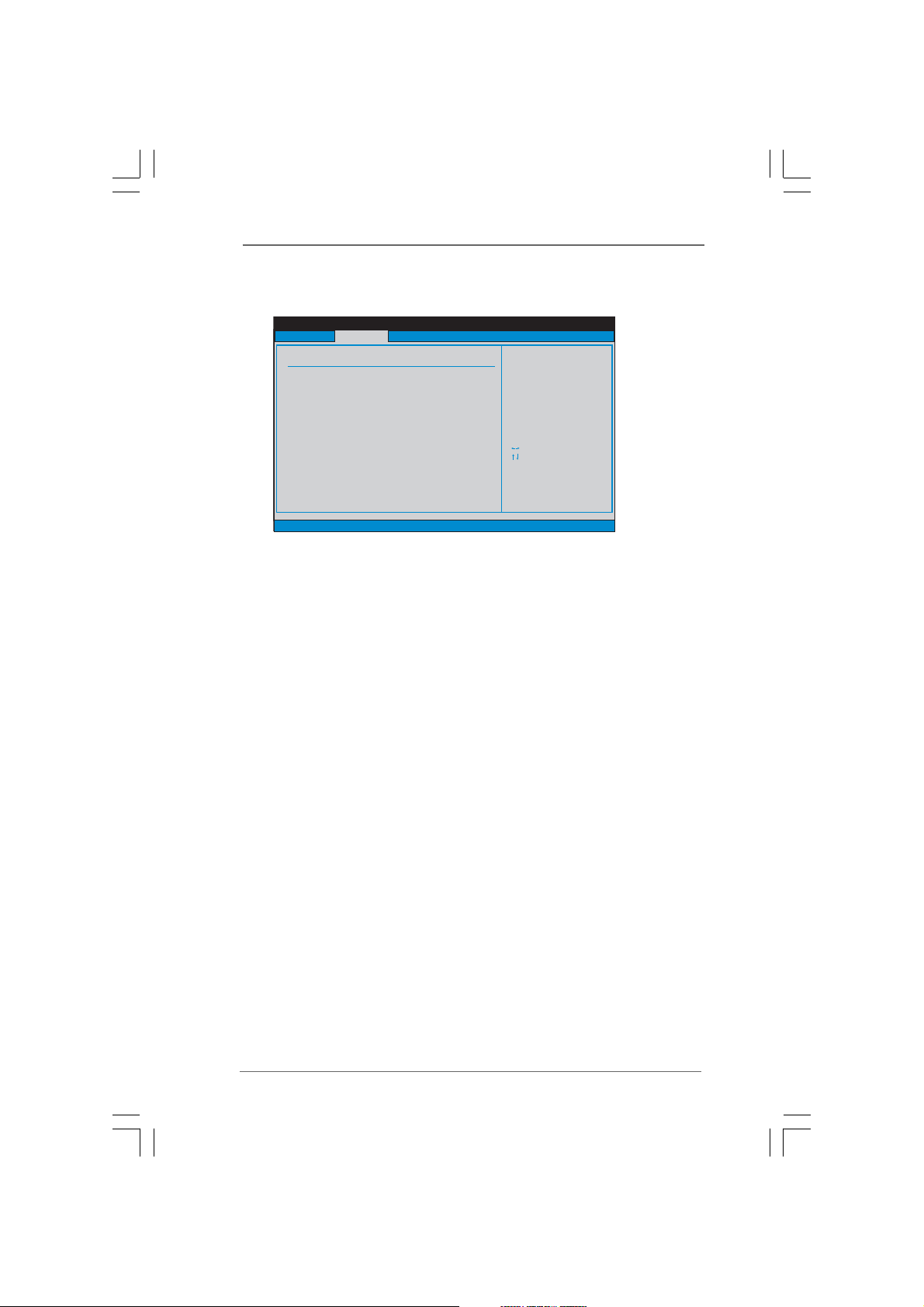
Enhance Halt State
All processors support the Halt State (C1). The C1 state is supported
through the native processor instructions HLT and MWAIT and requires no
hardware support from the chipset. In the C1 power state, the processor
maintains the context of the system caches.
Intel (R) Virtualization tech.
When this option is set to [Enabled], a VMM (Virtual Machine Architecture)
can utilize the additional hardware capabilities provided by Vanderpool
Technology. This option will be hidden if the installed CPU does not support
Intel (R) Virtualization Technology.
CPU Thermal Throttling
You may select [Enabled] to enable P4 CPU internal thermal control mecha-
nism to keep the CPU from overheated.
No-Excute Memory Protection
No-Execution (NX) Memory Protection Technology is an enhancement to
the IA-32 Intel Architecture. An IA-32 processor with “No Execute (NX)
Memory Protection” can prevent data pages from being used by malicious
software to execute code. This option will be hidden if the current CPU
does not support No-Excute Memory Protection.
Hyper Threading Technology
To enable this feature, it requires a computer system with an Intel Pentium
4 processor that supports Hyper-Threading technology and an operating
system that includes optimization for this technology, such as Microsoft
Windows® XP or VistaTM. Set to [Enabled] if using Microsoft® Windows® XP,
VistaTM, or Linux kernel version 2.4.18 or higher. This option will be hidden
if the installed CPU does not support Hyper-Threading technology.
®
®
3636
36
3636
Page 37

Intel (R) SpeedStep(tm) tech.
Intel (R) SpeedStep(tm) tech. is Intel’s new power saving technology.
Processor can switch between multiple frequency and voltage points to
enable power savings. The default value is [Auto]. Configuration options:
[Auto], [Enabled] and [Disabled]. If you install Windows® XP and select
[Auto], you need to set the “Power Schemes” as “Portable/Laptop” to en-
able this function. If you install Windows® VistaTM and want to enable this
function, please set this item to [Enabled]. This item will be hidden if the
current CPU does not support Intel (R) SpeedStep(tm) tech..
Please note that enabling this function may reduce CPU voltage and lead to system
stability or compatibility issue with some power supplies. Please set this item to
[Disable] if above issue occurs.
3737
37
3737
Page 38
3.4.23.4.2
Chipset ConfigurationChipset Configuration
3.4.2
Chipset Configuration
3.4.23.4.2
Chipset ConfigurationChipset Configuration
3838
38
3838
Advanced
Chipset Settings
Memory Remap Feature
Fixed Mode Operation
Primary Graphics Adapter
Shared Memory
PAVP Mode
DVMT Mode Select
DVMT/FIXED Memory
Onboard HD Audio
Front Panel
OnBoard Lan
Intelligent Energy Saver
v02.54 (C)Copyright 1985-2005, American Megatrends, Inc.
BIOS SETUP UTILITY
[Disabled]
[Enabled]
[PCI]
[Auto]
[Disabled]
[DVMT Mode]
[Maximum DVMT]
[Auto]
[Enabled]
[Enabled]
[Disabled]
ENABLE: Allow
remapping of
overlapped PCI memory
above the total
physical memory.
DISABLE: Do not allow
remapping of memory.
Select Screen
Select Item
+ - Change Option
F1 General Help
F9 Load Defaults
F10 Save and Exit
ESC Exit
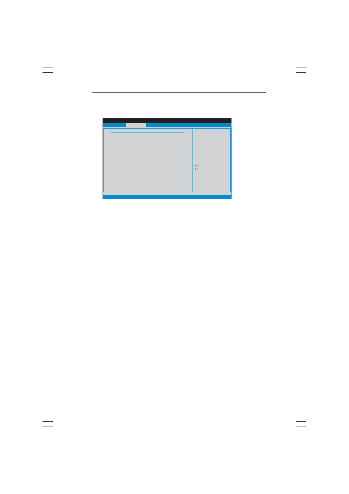
Memory Remap Feature
Use this item to enable or disable memory remap feature. Configuration
options: [Enabled] and [Disabled]. The default value is [Disabled].
Flex Mode Operation
This allows you to enable or disable flex mode operation feature. The
default value is [Enabled]. Configuration options: [Enabled] and [Disabled].
Primary Graphics Adapter
This allows you to select [Onboard], [PCI] or [PCI Express] as the boot
graphic adapter priority. The default value is [PCI].
Share Memory
This allows you to set share memory feature. The default value is [Auto].
Configuration options: [Auto], [32MB], [64MB], [128MB] and [256MB].
PAVP Mode
Use this option to adjust PAVP mode. Configuration options: [Disabled] and
[Lite]. The default value is [Disabled]. PAVP is the new graphics feature in
Intel® 4 Series Express chipset family to support increased content
protection and robustness requirements for premium content playback (Blu-
ray disc). [Lite] mode is the encryption of compressed video buffer and is
hardware-based 128-bit AES decryption.
DVMT Mode Select
Use this option to adjust DVMT mode. The default value is [DVMT Mode].
DVMT (Dynamic Video Memory Technology) is an architecture that offers
breakthrough performance for the motherboard through efficient memory
utilization. In DVMT mode, the graphics driver allocates memory as needed
for running graphics applications and is cooperatively using this memory
with other system components. This item will not be used under Windows
VistaTM OS because the driver will intelligently detect physical memory
available and allocate necessary video memory.
®
Page 39

DVMT/FIXED Memory
You are allowed to adjust the shared memory size in this item if you set
DVMT Mode Select as [DVMT Mode]. Configuration options: [128MB], [256MB]
and [Maximum DVMT]. The option [Maximum DVMT] only appears when you
adopt the memory module with 1024MB or above.
Onboard HD Audio
Select [Auto], [Enabled] or [Disabled] for the onboard HD Audio feature. If
you select [Auto], the onboard HD Audio will be disabled when PCI Sound
Card is plugged.
Front Panel
Select [Auto], [Enabled] or [Disabled] for the onboard HD Audio Front Panel.
OnBoard Lan
This allows you to enable or disable the “OnBoard Lan” feature.
Intelligent Energy Saver
Intelligent Energy Saver is a revolutionary technology that delivers
unparalleled power savings. The default value is [Enabled]. Configuration
options: [Auto], [Enabled] and [Disabled]. If you want to enable this function,
please set this item to [Enabled]. Besides the BIOS option, you can also
choose our Intelligent Energy Saver utility to enable this function.
3939
39
3939
Page 40
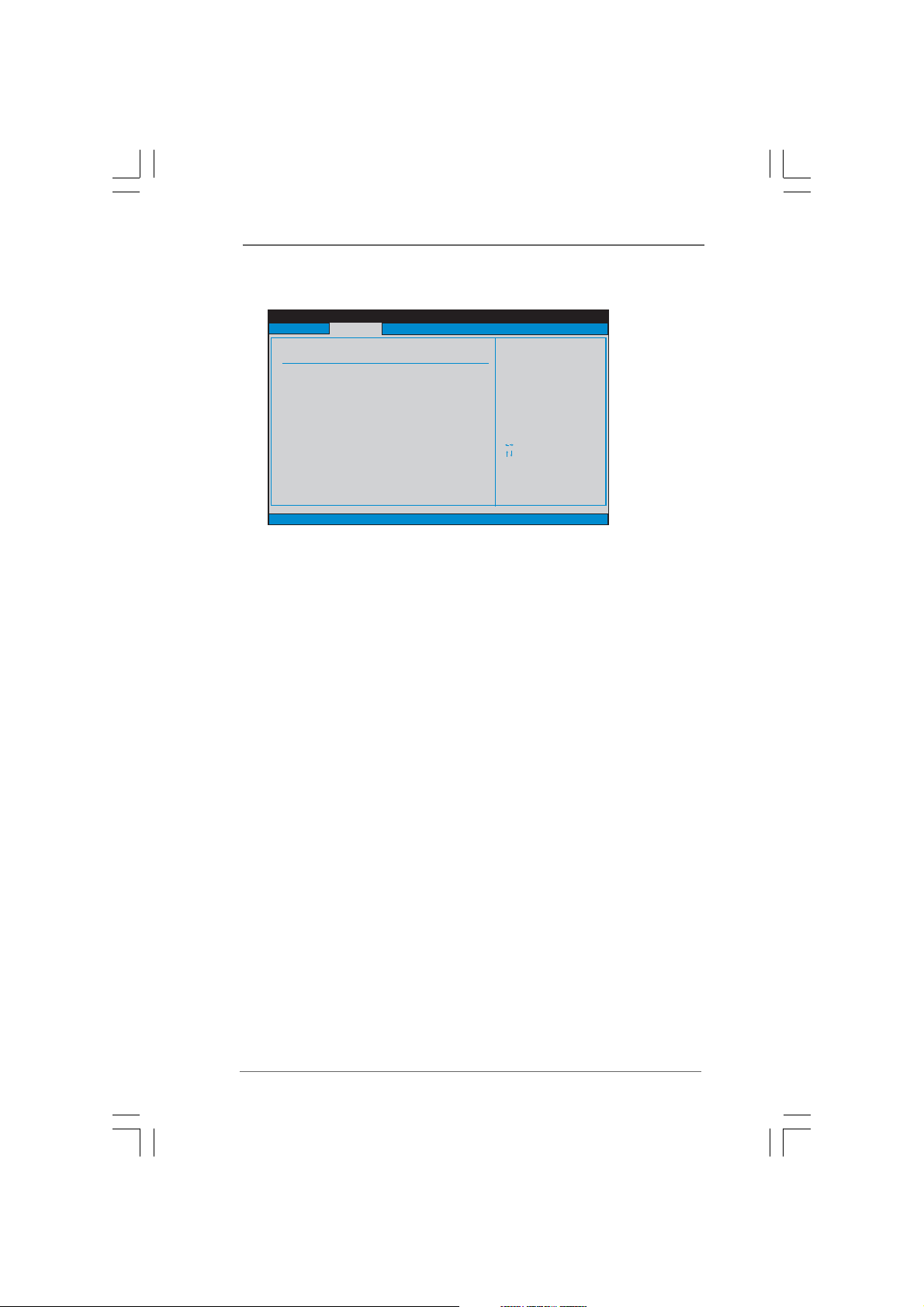
3.4.33.4.3
ACPI ConfigurationACPI Configuration
3.4.3
ACPI Configuration
3.4.33.4.3
ACPI ConfigurationACPI Configuration
Advanced
ACPI Configuration
Suspend To RAM
Restore onAC/Power Loss
Ring-In Power On
PCI Devices Power On
PS /2 Keyboard Power On
RTC Alarm Power On
ACPI HPET Table
v02.54 (C)Copyright 1985-2005, American Megatrends, Inc.
BIOS SETUP UTILITY
[Disabled]
[Power Off]
[Disabled]
[Disabled]
[Disabled]
[Disabled]
[Disabled]
Select auto-detect or
disable the STR
feature.
Select Screen
Select Item
+- Change Option
F1 General Help
F9 Load Defaults
F10 Save and Exit
ESC Exit
Suspend to RAM
Use this item to select whether to auto-detect or disable the Suspend-to-
RAM feature. Select [Auto] will enable this feature if the OS supports it. If
you set this item to [Disabled], the function “Repost Video on STR Resume”
will be hidden.
Repost Video on STR Resume
This feature allows you to repost video on STR resume. (STR refers to
suspend to RAM.)
Check Ready Bit
Use this item to enable or disable the feature Check Ready Bit.
Restore on AC/Power Loss
This allows you to set the power state after an unexpected AC/Power
loss. If [Power Off] is selected, the AC/Power remains off when the power
recovers. If [Power On] is selected, the AC/Power resumes and the
system starts to boot up when the power recovers.
Ring-In Power On
Use this item to enable or disable Ring-In signals to turn on the system from
the power-soft-off mode.
PCI Devices Power On
Use this item to enable or disable PCI devices to turn on the system from the
power-soft-off mode.
PS/2 Keyboard Power On
Use this item to enable or disable PS/2 keyboard to turn on the system from
the power-soft-off mode.
RTC Alarm Power On
Use this item to enable or disable RTC (Real Time Clock) to power on the
system.
4040
40
4040
Page 41
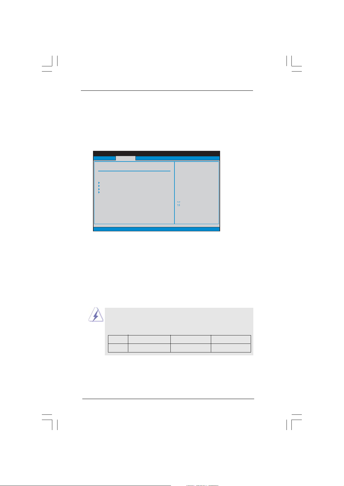
ACPI HPET Table
Use this item to enable or disable ACPI HPET Table. The default value is
[Disabled]. Please set this option to [Enabled] if you plan to use this
motherboard to submit Windows® VistaTM certification.
3.4.43.4.4
Storage ConfigurationStorage Configuration
3.4.4
Storage Configuration
3.4.43.4.4
Storage ConfigurationStorage Configuration
Advanced
Storage Configuration
ATA/IDE Configuration
SATAII_1
SATAII_2
IDE1 Master
IDE1 Slave
v02.54 (C)Copyright 1985-2005, American Megatrends, Inc.
BIOS SETUP UTILITY
[Enhanced]
[Hard Disk]
[Not Detected]
[Not Detected]
[Not Detected]
Set [Compatible]
when Legacy OS
(MS-DOS, Win NT)
device is used.
Set [Enhanced]
when Native OS
(Win2000 /XP)
is used.
Select Screen
Select Screen
Select Item
Select Item
+- Change Option
+- Change Option
F1 General Help
F1 General Help
F9 Load Defaults
F9 Load Defaults
F10 Save and Exit
F10 Save and Exit
ESC Exit
ESC Exit
ATA/IDE Configuration
Please select [Compatible] when you install legacy OS (Windows
native OS (Windows® 2000 / XP / VistaTM) is installed, please select
[Enhanced].
When [Compatible] is selected
Combined Option
It allows you to select between [SATA 1, SATA 2], [SATA 1, IDE 1], and
[IDE 1, SATA 2]. If it is set to [SATA 1, IDE 1], then SATAII_2 will not work.
Likewise, if it is set to [IDE 1, SATA 2], then SATAII_1 will not work.
®
NT). If
Because Intel® ICH7 south bridge only supports two IDE devices
under legacy OS (Windows NT), you have to choose [SATA 1, SATA2],
[SATA 1, IDE 1], or [IDE 1, SATA 2] when the installed device is used
with legacy OS.
[SATA 1, SATA 2] [SATA 1, IDE 1] [IDE 1, SATA 2]
Master SATAII 1, SATAII 2 SATAII 1 SATAII 2
IDE Device Configuration
You may set the IDE configuration for the device that you specify. We will
use the “Primary IDE Master” as the example in the following instruction.
4141
41
4141
Page 42
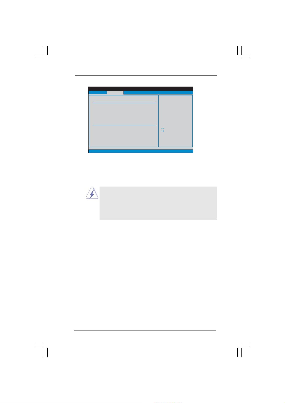
Advanced
Primary IDE Master
Device
Vendor
Size
LBA Mode
Block Mode
PIO Mode
Async DMA
Ultra DMA
S.M.A.R.T.
Type
LBA/Large Mode
Block (Multi-Sector Transfer)
PIO Mode
DMA Mode
S.M.A.R.T.
32Bit Data Transfer
v02.54 (C)Copyright 1985-2005, American Megatrends, Inc.
BIOS SETUP UTILITY
:Hard Disk
:ST340014A
:40.0 GB
:Supported
:16Sectors
:4
:MultiWord DMA-2
:Ultra DMA-5
:Supported
[Auto]
[Auto]
[Auto]
[Auto]
[Auto]
[Disabled]
[Enabled]
Select the type
of device connected
to the system.
Select Screen
Select Item
+- Change Option
F1 General Help
F9 Load Defaults
F10 Save and Exit
ESC Exit
TYPE
Use this item to configure the type of the IDE device that you specify.
Configuration options: [Not Installed], [Auto], [CD/DVD], and [ARMD].
[Not Installed]: Select [Not Installed] to disable the use of IDE device.
[Auto]: Select [Auto] to automatically detect the hard disk drive.
After selecting the hard disk information into BIOS, use a disk
utility, such as FDISK, to partition and format the new IDE hard
disk drives. This is necessary so that you can write or read
data from the hard disk. Make sure to set the partition of the
Primary IDE hard disk drives to active.
[CD/DVD]: This is used for IDE CD/DVD drives.
[ARMD]: This is used for IDE ARMD (ATAPI Removable Media Device),
such as MO.
LBA/Large Mode
Use this item to select the LBA/Large mode for a hard disk > 512 MB under
DOS and Windows; for Netware and UNIX user, select [Disabled] to
disable the LBA/Large mode.
Block (Multi-Sector Transfer)
The default value of this item is [Auto]. If this feature is enabled, it will
enhance hard disk performance by reading or writing more data during
each transfer.
PIO Mode
Use this item to set the PIO mode to enhance hard disk performance by
optimizing the hard disk timing.
DMA Mode
DMA capability allows the improved transfer-speed and data-integrity for
compatible IDE devices.
4242
42
4242
Page 43
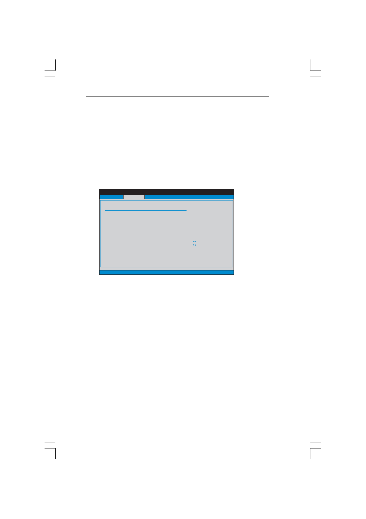
S.M.A.R.T.
Use this item to enable or disable the S.M.A.R.T. (Self-Monitoring, Analysis,
and Reporting Technology) feature. Configuration options: [Disabled], [Auto],
[Enabled].
32-Bit Data Transfer
Use this item to enable 32-bit access to maximize the IDE hard disk data
transfer rate.
3.4.53.4.5
PCIPnP ConfigurationPCIPnP Configuration
3.4.5
PCIPnP Configuration
3.4.53.4.5
PCIPnP ConfigurationPCIPnP Configuration
Advanced
Advanced PCI / PnP Settings
PCI Latency Timer
PCI IDE BusMaster
v02.54 (C)Copyright 1985-2005, American Megatrends, Inc.
BIOS SETUP UTILITY
[32]
[Enabled]
ValueinunitsofPCI
clocks for PCI device
latency timer
register.
Select Screen
Select Item
+- Change Option
F1 General Help
F9 Load Defaults
F10 Save and Exit
ESC Exit
PCI Latency Timer
The default value is 32. It is recommended to keep the default value unless
the installed PCI expansion cards’ specifications require other settings.
PCI IDE BusMaster
Use this item to enable or disable the PCI IDE BusMaster feature.
4343
43
4343
Page 44
3.4.63.4.6
Super IO ConfigurationSuper IO Configuration
3.4.6
Super IO Configuration
3.4.63.4.6
Super IO ConfigurationSuper IO Configuration
Advanced
Configure Super IO Chipset
Serial Port Address [3F8 /IRQ4]
Parallel Port Address
Parallel Port Mode
EPP Version
ECP Mode DMA Channel
Parallel Port IRQ
v02.54 (C)Copyright 1985-2003, American Megatrends, Inc.
BIOS SETUP UTILITY
[378]
[ECP + EPP]
[1.9]
[DMA3]
[IRQ7]
Allow BIOS to Enable
or Disable Floppy
Controller.
Select Screen
Select Item
+- Change Option
F1 General Help
F9 Load Defaults
F10 Save and Exit
ESC Exit
Serial Port Address
Use this item to set the address for the onboard serial port or disable it.
Configuration options: [Disabled], [3F8 / IRQ4], [2F8 / IRQ3], [3E8 / IRQ4],
[2E8 / IRQ3].
Parallel Port Address
Use this item to set the address for the onboard parallel port or disable it.
Configuration options: [Disabled], [378], and [278].
Parallel Port Mode
Use this item to set the operation mode of the parallel port. The default
value is [ECP+EPP]. If this option is set to [ECP+EPP], it will show the EPP
version in the following item, “EPP Version”. Configuration options:
[Normal], [Bi-Directional], and [ECP+EPP].
EPP Version
Use this item to set the EPP version. Configuration options: [1.9]
and [1.7].
ECP Mode DMA Channel
Use this item to set the ECP mode DMA channel. Configuration
options: [DMA0], [DMA1], and [DMA3].
Parallel Port IRQ
Use this item to set the IRQ for the parallel port. Configuration options:
[IRQ5] and [IRQ7].
4444
44
4444
Page 45
3.4.73.4.7
USB ConfigurationUSB Configuration
3.4.7
USB Configuration
3.4.73.4.7
USB ConfigurationUSB Configuration
Advanced
USB Configuration
USB Controller
USB 2.0 Support
Legacy USB Support
v02.54 (C)Copyright 1985-2005, American Megatrends, Inc.
BIOS SETUP UTILITY
[Enabled]
[Enabled]
[Enabled]
To enable or disable
the onboard USB
controllers.
Select Screen
Select Item
+- Change Option
F1 General Help
F9 Load Defaults
F10 Save and Exit
ESC Exit
USB Controller
Use this item to enable or disable the use of USB controller.
USB 2.0 Support
Use this item to enable or disable the USB 2.0 support.
Legacy USB Support
Use this option to select legacy support for USB devices. There are four
configuration options: [Enabled], [Auto], [Disabled] and [BIOS Setup
Only]. The default value is [Enabled]. Please refer to below descriptions
for the details of these four options:
[Enabled] - Enables support for legacy USB.
[Auto] - Enables legacy support if USB devices are connected.
[Disabled] - USB devices are not allowed to use under legacy OS and BIOS
setup when [Disabled] is selected. If you have USB compatibility issue, it is
recommended to select [Disabled] to enter OS.
[BIOS Setup Only] - USB devices are allowed to use only under BIOS setup
and Windows® / Linux OS.
4545
45
4545
Page 46
3.53.5
Hardware Health Event Monitoring ScreenHardware Health Event Monitoring Screen
3.5
Hardware Health Event Monitoring Screen
3.53.5
Hardware Health Event Monitoring ScreenHardware Health Event Monitoring Screen
In this section, it allows you to monitor the status of the hardware on your system,
including the parameters of the CPU temperature, motherboard temperature, CPU fan
speed, chassis fan speed, and the critical voltage.
Main Smart Advanced
Hardware Health Event Monitoring
CPU Temperature
M /B Temperature
CPU Fan Speed
Chassis Fan Speed
Vcore
+ 3.30V
+ 5.00V
+ 12.00V
CPU Quiet Fan [Disabled]
v02.54 (C)Copyright 1985-2003, American Megatrends, Inc.
BIOS SETUP UTILITY
H/W Monitor
: 37C/98F
: 31C/87F
: 3400 RPM
:N/A
: 1.629V
: 3.306V
: 5.067V
: 11.890V
Boot Security Exit
Enable/Disable
CPU Quiet Fan
Function.
Select Screen
Select Item
F1 General Help
F9 Load Defaults
F10 Save and Exit
ESC Exit
CPU Quiet Fan
This item allows you to identify the temperature of CPU fan. If you set this
option as [Disabled], the CPU fan will operate in full speed. If you set this
option as [Enabled], you will find the items “Target CPU Temperature” and
“Target Fan Speed” appear to allow you adjusting them. The default value
is [Disabled]. You are allowed to enable this function only when you install
4-pin CPU fan.
Target CPU Temperature
The target temperature will be between 45 C/113 F and 65 C/149 F.
The default value is [50 C/122 F].
Target Fan Speed
Use this option to set the target fan speed. You can freely adjust the
target fan speed according to the target CPU temperature that you
choose. The default value is [Fast]. Configuration options: [Fast], [Middle]
and [Slow].
4646
46
4646
Page 47
3.63.6
Boot ScreenBoot Screen
3.6
Boot Screen
3.63.6
Boot ScreenBoot Screen
In this section, it will display the available devices on your system for you to config-
ure the boot settings and the boot priority.
Main Smart Advanced H/W Monitor
Boot Settings
Boot Settings Configuration
1st Boot Device
2nd Boot Device
3rd Boot Device
4th Boot Device
Hard Disk Drives
Removable Drives
CD/DVD Drives
v02.54 (C)Copyright 1985-2005, American Megatrends, Inc.
3.6.13.6.1
3.6.1
3.6.13.6.1
Boot Settings ConfigurationBoot Settings Configuration
Boot Settings Configuration
Boot Settings ConfigurationBoot Settings Configuration
Boot Settings Configuration
Full Screen Logo
AddOn ROM Display
Boot Logo
Boot From Onboard LAN
Bootup Num-Lock
BIOS SETUP UTILITY
[1st Floppy Device]
[HDD: PM -HDS722580VL]
[CD/DVD: 3S-CD-ROM C]
[USB]
BIOS SETUP UTILITY
[Enabled]
[Enabled]
[Auto]
[Disabled]
[On]
Boot
Configure Settings
during System Boot.
Enter Go to Sub Screen
F1 General Help
F9 Load Defaults
F10 Save and Exit
ESC Exit
Boot
Disabled: Displays
normal POST messages.
Enabled: Displays OEM
Logo instead of POST
messages.
+ - Change Option
F1 General Help
F9 Load Defaults
F10 Save and Exit
ESC Exit
Security Exit
Select Screen
Select Item
Select Screen
Select Item
v02.54 (C)Copyright 1985-2003, American Megatrends, Inc.
Full Screen Logo
Use this item to enable or disable OEM Logo. The default value is [Enabled].
AddOn ROM Display
Use this option to adjust AddOn ROM Display. If you enable the option
“Full Screen Logo” but you want to see the AddOn ROM information when
the system boots, please select [Enabled]. Configuration options: [Enabled]
and [Disabled]. The default value is [Enabled].
4747
47
4747
Page 48
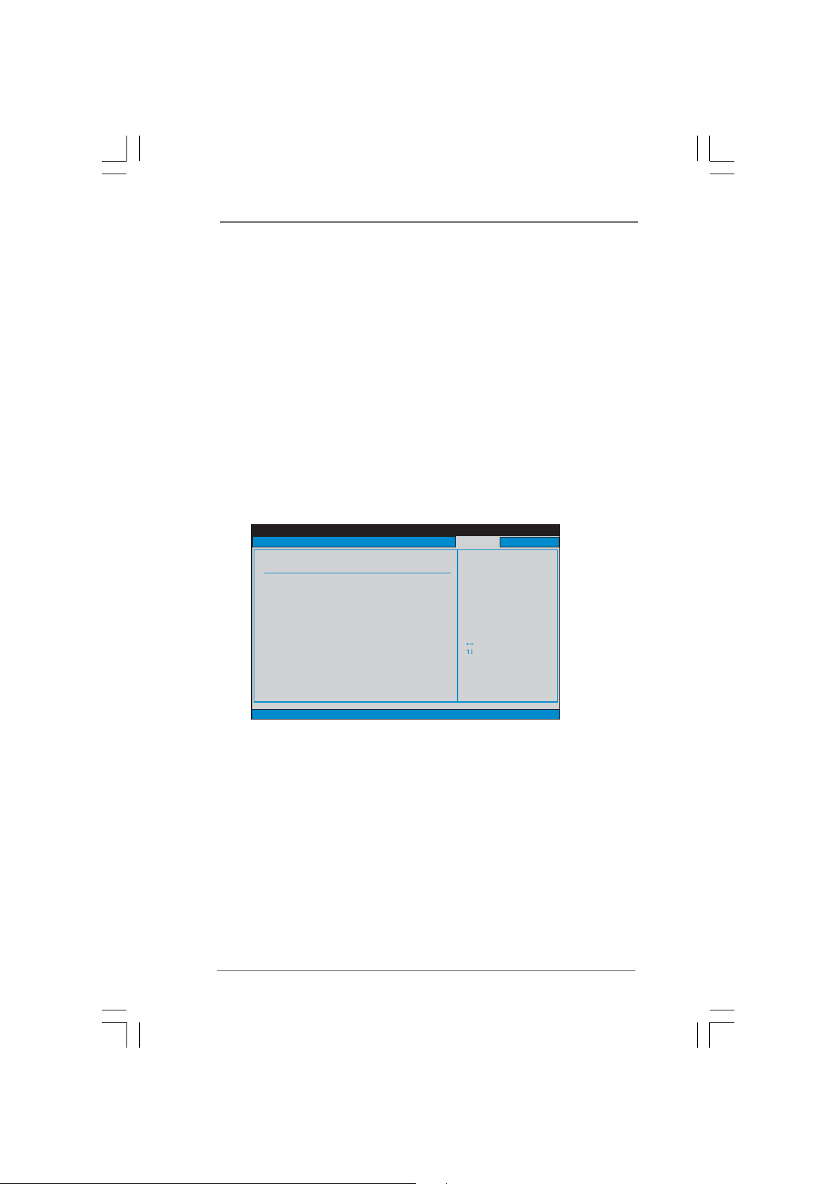
Boot Logo
Use this option to select logo in POST screen. This option only appears
when you enable the option “Full Screen Logo”. Configuration options:
[Auto], [S series], [Scenery] and [ASRock]. The default value is [Auto].
Currently, the option [Auto] is set to Aircraft.
Boot From Onboard LAN
Use this item to enable or disable the Boot From Onboard LAN feature.
Boot Up Num-Lock
If this item is set to [On], it will automatically activate the Numeric Lock
function after boot-up.
3.73.7
Security ScreenSecurity Screen
3.7
Security Screen
3.73.7
Security ScreenSecurity Screen
In this section, you may set or change the supervisor/user password for the system.
For the user password, you may also clear it.
Main Smart Advanced H/W Monitor Boot
Security Settings
Supervisor Password :Not Installed
User Password : Not Installed
Change Supervisor Password
Change User Password
v02.54 (C)Copyright 1985-2005, American Megatrends, Inc.
BIOS SETUP UTILITY
Security
Install or Change the
password.
Enter Change
F1 General Help
F9 Load Defaults
F10 Save and Exit
ESC Exit
Exit
Select Screen
Select Item
4848
48
4848
Page 49
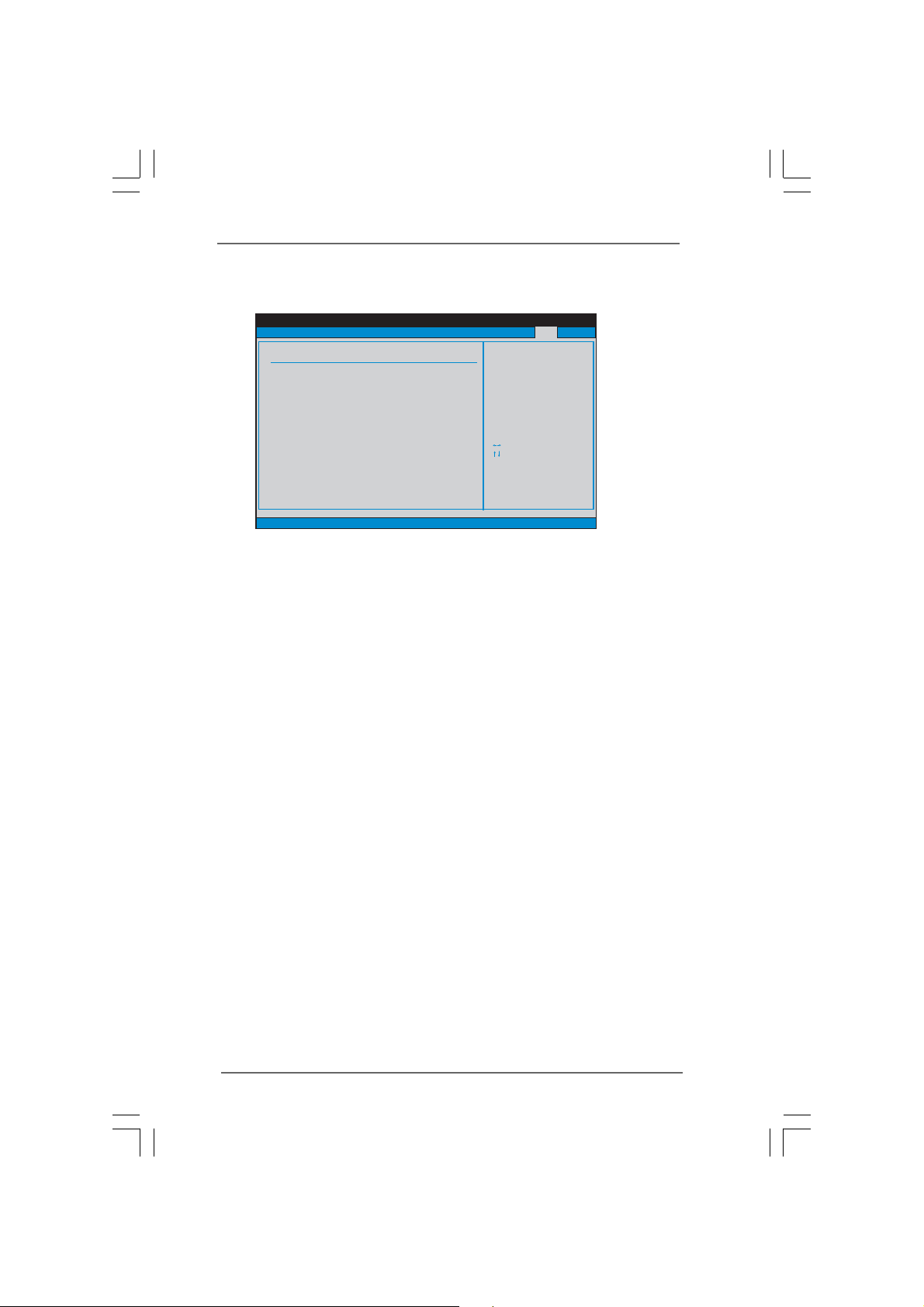
3.83.8
Exit ScreenExit Screen
3.8
Exit Screen
3.83.8
Exit ScreenExit Screen
Main OC Tweaker Advanced H/W Monitor Boot Security
Exit Options
Save Changes and Exit
Discard Changes and Exit
Discard Changes
Load BIOS Defaults
Load Performance Setup Default (IDE/SATA)
Load Power Saving Setup Default
v02.54 (C)Copyright 1985-2005, American Megatrends, Inc.
BIOS SETUP UTILITY
Exit
Exit system setup
after saving the
changes.
F10 key can be used
for this operation.
Select Screen
Select Item
Enter Go to Sub Screen
F1 General Help
F9 Load Defaults
F10 Save and Exit
ESC Exit
Save Changes and Exit
When you select this option, it will pop-out the following message, “Save
configuration changes and exit setup?” Select [OK] to save the changes
and exit the BIOS SETUP UTILITY.
Discard Changes and Exit
When you select this option, it will pop-out the following message, “Dis-
card changes and exit setup?” Select [OK] to exit the BIOS SETUP UTILITY
without saving any changes.
Discard Changes
When you select this option, it will pop-out the following message, “Dis-
card changes?” Select [OK] to discard all changes.
Load BIOS Defaults
Load BIOS default values for all the setup questions. F9 key can be used
for this operation.
Load Performance Setup Default (IDE/SATA)
This performance setup default may not be compatible with all system
configurations. If system boot failure occurs after loading, please resume
optimal default settings. F5 key can be used for this operation.
Load Power Saving Setup Default
Load power saving setup default. F6 key can be used for this operation.
4949
49
4949
Page 50

Chapter 4 SofChapter 4 Sof
Chapter 4 Sof
Chapter 4 SofChapter 4 Sof
4.14.1
Install Operating SystemInstall Operating System
4.1
Install Operating System
4.14.1
Install Operating SystemInstall Operating System
This motherboard supports various Microsoft® Windows® operating systems: 2000 /
XP / XP 64-bit / VistaTM / Vista
hardware options vary, use the setup procedures in this chapter for general refer-
ence only. Refer to your OS documentation for more information.
4.24.2
Support CD InformationSupport CD Information
4.2
Support CD Information
4.24.2
Support CD InformationSupport CD Information
The Support CD that came with the motherboard contains necessary drivers and
useful utilities that enhance the motherboard features.
4.2.14.2.1
Running The Support CDRunning The Support CD
4.2.1
Running The Support CD
4.2.14.2.1
Running The Support CDRunning The Support CD
To begin using the support CD, insert the CD into your CD-ROM drive. The CD
automatically displays the Main Menu if “AUTORUN” is enabled in your computer.
If the Main Menu did not appear automatically, locate and double click on the
file “ASSETUP.EXE” from the BIN folder in the Support CD to display the menus.
4.2.24.2.2
Drivers MenuDrivers Menu
4.2.2
Drivers Menu
4.2.24.2.2
Drivers MenuDrivers Menu
The Drivers Menu shows the available devices drivers if the system detects
installed devices. Please install the necessary drivers to activate the devices.
4.2.34.2.3
Utilities MenuUtilities Menu
4.2.3
Utilities Menu
4.2.34.2.3
Utilities MenuUtilities Menu
The Utilities Menu shows the applications software that the motherboard
supports. Click on a specific item then follow the installation wizard to install it.
TM
64-bit / Win7. Because motherboard settings and
tware Supportware Suppor
tware Suppor
tware Supportware Suppor
tt
t
tt
5050
50
5050
4.2.44.2.4
Contact InformationContact Information
4.2.4
Contact Information
4.2.44.2.4
Contact InformationContact Information
If you need to contact ASRock or want to know more about ASRock, welcome
to visit ASRock’s website at http://www.asrock.com; or you may contact your
dealer for further information.
 Loading...