

Page 1

RealView Platform Baseboard for
ARM926EJ-S
HBI-0117
User Guide
™
Copyright © 2003-2010 ARM Limited. All rights reserved.
ARM DUI 0224I
Page 2

RealView Platform Baseboard for ARM926EJ-S
User Guide
Copyright © 2003-2010 ARM Limited. All rights reserved.
Release Information
Change History
Date Issue Confidentiality Change
November 2003 A Non-Confidential First release.
April 2004 B Non-Confidential Second release. Added configuration details for USB
November 2005 C Non-Confidential Third release. Corrected reported defects and added
debug, PCI, and Boot Monitor.
requested enhancements.
August 2006 D Non-Confidential Fourth release. Corrected reported defects and added
May 2007 E Non-Confidential Fifth release. Corrected reported defects and added
October 2007 F Non-Confidential Sixth release. Corrected reported defect.
April 2008 G Non-Confidential Seventh release. Corrected reported defect.
March 2009 H Non-Confidential Eighth release. Corrected reported defect.
July 2010 I Non-Confidential Ninth release. Document update.
requested enhancements.
requested enhancements.
Proprietary Notice
®
Words and logos marked with
or ™ are registered trademarks or trademarks owned by ARM Limited, except
as otherwise stated below in this proprietary notice. Other brands and names mentioned herein may be the
trademarks of their respective owners.
Neither the whole nor any part of the information contained in, or the product described in, this document
may be adapted or reproduced in any material form except with the prior written permission of the copyright
holder.
The product described in this document is subject to continuous developments and improvements. All
particulars of the product and its use contained in this document are given by ARM in good faith. However,
all warranties implied or expressed, including but not limited to implied warranties of merchantability, or
fitness for purpose, are excluded.
This document is intended only to assist the reader in the use of the product. ARM Limited shall not be liable
for any loss or damage arising from the use of any information in this document, or any error or omission in
such information, or any incorrect use of the product.
ii Copyright © 2003-2010 ARM Limited. All rights reserved. ARM DUI 0224I
Page 3

Confidentiality Status
This document is Non-Confidential. The right to use, copy and disclose this document may be subject to
license restrictions in accordance with the terms of the agreement entered into by ARM and the party that
ARM delivered this document to.
Product Status
The information in this document is final, that is for a developed product.
Web Address
http://www.arm.com
ARM DUI 0224I Copyright © 2003-2010 ARM Limited. All rights reserved. iii
Page 4

Note
Conformance Notices
This section contains conformance notices.
Federal Communications Commission Notice
This device is test equipment and consequently is exempt from part 15 of the FCC Rules under section 15.103
(c).
CE Declaration of Conformity
The system should be powered down when not in use.
The PB926EJ-S generates, uses, and can radiate radio frequency energy and may cause harmful interference
to radio communications. However, there is no guarantee that interference will not occur in a particular
installation. If this equipment causes harmful interference to radio or television reception, which can be
determined by turning the equipment off or on, you are encouraged to try to correct the interference by one
or more of the following measures:
• ensure attached cables do not lie across the card
• reorient the receiving antenna
• increase the distance between the equipment and the receiver
• connect the equipment into an outlet on a circuit different from that to which the receiver is connected
• consult the dealer or an experienced radio/TV technician for help
It is recommended that wherever possible shielded interface cables be used.
iv Copyright © 2003-2010 ARM Limited. All rights reserved. ARM DUI 0224I
Page 5

Contents
RealView Platform Baseboard for ARM926EJ-S
User Guide
Preface
About this manual ...................................................................................... xviii
Feedback .................................................................................................... xxv
Chapter 1 Introduction
1.1 About the PB926EJ-S ................................................................................. 1-2
1.2 PB926EJ-S architecture .............................................................................. 1-4
1.3 Precautions ................................................................................................. 1-9
Chapter 2 Getting Started
2.1 Setting up the RealView Platform ............................................................... 2-2
2.2 Setting the configuration switches .............................................................. 2-3
2.3 Connecting JTAG debugging equipment .................................................... 2-8
2.4 Connecting the Trace Port Analyzer ......................................................... 2-10
2.5 Supplying power ....................................................................................... 2-13
2.6 Using the PB926EJ-S Boot Monitor and platform library .......................... 2-14
Chapter 3 Hardware Description
3.1 ARM926EJ-S PXP Development Chip ........................................................ 3-3
3.2 FPGA ........................................................................................................ 3-17
ARM DUI 0224I Copyright © 2003-2010 ARM Limited. All rights reserved. v
Page 6

Contents
3.3 Reset controller ........................................................................................ 3-22
3.4 Power supply control ................................................................................ 3-33
3.5 Clock architecture ..................................................................................... 3-35
3.6 Advanced Audio Codec Interface, AACI ................................................... 3-56
3.7 Character LCD controller .......................................................................... 3-59
3.8 CLCDC interface ...................................................................................... 3-61
3.9 DMA .......................................................................................................... 3-65
3.10 Ethernet interface ..................................................................................... 3-68
3.11 GPIO interface .......................................................................................... 3-71
3.12 Interrupts .................................................................................................. 3-72
3.13 Keyboard/Mouse Interface, KMI ............................................................... 3-74
3.14 Memory Card Interface, MCI .................................................................... 3-75
3.15 PCI interface ............................................................................................. 3-79
3.16 Serial bus interface ................................................................................... 3-80
3.17 Smart Card interface, SCI ........................................................................ 3-81
3.18 Synchronous Serial Port, SSP .................................................................. 3-84
3.19 User switches and LEDs .......................................................................... 3-87
3.20 UART interface ......................................................................................... 3-88
3.21 USB interface ........................................................................................... 3-92
3.22 Test, configuration, and debug interfaces ................................................ 3-94
Chapter 4 Programmer’s Reference
4.1 Memory map ............................................................................................... 4-3
4.2 Configuration and initialization .................................................................... 4-9
4.3 Status and system control registers ......................................................... 4-17
4.4 AHB monitor ............................................................................................. 4-41
4.5 Advanced Audio CODEC Interface, AACI ................................................ 4-42
4.6 Character LCD display ............................................................................. 4-44
4.7 Color LCD Controller, CLCDC .................................................................. 4-47
4.8 Direct Memory Access Controller and mapping registers ........................ 4-52
4.9 Ethernet .................................................................................................... 4-55
4.10 General Purpose Input/Output, GPIO ....................................................... 4-56
4.11 Interrupt controllers ................................................................................... 4-57
4.12 Keyboard and Mouse Interface, KMI ........................................................ 4-67
4.13 MBX .......................................................................................................... 4-68
4.14 MOVE video coprocessor ......................................................................... 4-69
4.15 MultiMedia Card Interfaces, MCIx ............................................................ 4-70
4.16 MultiPort Memory Controller, MPMC ........................................................ 4-71
4.17 PCI controller ............................................................................................ 4-74
4.18 Real Time Clock, RTC .............................................................................. 4-85
4.19 Serial bus interface ................................................................................... 4-86
4.20 Smart Card Interface, SCI ........................................................................ 4-88
4.21 Synchronous Serial Port, SSP .................................................................. 4-89
4.22 Synchronous Static Memory Controller, SSMC ........................................ 4-91
4.23 System Controller ..................................................................................... 4-95
4.24 Timers ....................................................................................................... 4-96
4.25 UART ........................................................................................................ 4-97
vi Copyright © 2003-2010 ARM Limited. All rights reserved. ARM DUI 0224I
Page 7

4.26 USB interface ............................................................................................ 4-99
4.27 Vector Floating Point, VFP9 .................................................................... 4-100
4.28 Watchdog ................................................................................................ 4-101
Appendix A Signal Descriptions
A.1 Synchronous Serial Port interface ............................................................... A-2
A.2 Smart Card interface ................................................................................... A-3
A.3 UART interface ........................................................................................... A-5
A.4 USB interface .............................................................................................. A-6
A.5 Audio CODEC interface .............................................................................. A-7
A.6 MMC and SD flash card interface ............................................................... A-8
A.7 CLCD display interface ............................................................................. A-10
A.8 VGA display interface ............................................................................... A-13
A.9 GPIO interface .......................................................................................... A-14
A.10 Keyboard and mouse interface ................................................................. A-15
A.11 Ethernet interface ...................................................................................... A-16
A.12 RealView Logic Tile header connectors .................................................... A-17
A.13 Test and debug connections ..................................................................... A-33
Appendix B Specifications
B.1 Electrical specification ................................................................................. B-2
B.2 Clock rate restrictions .................................................................................. B-5
B.3 Mechanical details ...................................................................................... B-9
Contents
Appendix C CLCD Display and Adaptor Board
C.1 About the CLCD display and adaptor board .............................................. C-2
C.2 Installing the CLCD display ........................................................................ C-6
C.3 Touchscreen controller interface .............................................................. C-11
C.4 Connectors ............................................................................................... C-15
C.5 Mechanical layout .................................................................................... C-19
Appendix D PCI Backplane and Enclosure
D.1 Connecting the PB926EJ-S to the PCI enclosure ...................................... D-2
D.2 Backplane hardware .................................................................................. D-6
D.3 Connectors ............................................................................................... D-10
Appendix E Memory Expansion Boards
E.1 About memory expansion ........................................................................... E-2
E.2 Fitting a memory board ............................................................................... E-5
E.3 EEPROM contents ...................................................................................... E-6
E.4 Connector pinout ....................................................................................... E-13
E.5 Mechanical layout ..................................................................................... E-20
Appendix F RealView Logic Tile
F.1 About the RealView Logic Tile .................................................................... F-2
F.2 Fitting a RealView Logic Tile ....................................................................... F-3
ARM DUI 0224I Copyright © 2003-2010 ARM Limited. All rights reserved. vii
Page 8

Contents
F.3 Header connectors ..................................................................................... F-4
Appendix G Configuring the USB Debug Connection
G.1 Installing the RealView ICE Micro Edition driver ........................................ G-2
G.2 Changes to RealView Debugger ................................................................ G-5
G.3 Using the USB debug port to connect RealView Debugger ....................... G-6
G.4 Using the Debug tab of the RealView Debugger Register pane .............. G-10
viii Copyright © 2003-2010 ARM Limited. All rights reserved. ARM DUI 0224I
Page 9

List of Tables
RealView Platform Baseboard for ARM926EJ-S
User Guide
Change History ............................................................................................................. ii
Table 2-1 Selecting the boot device .......................................................................................... 2-4
Table 2-2 Default switch positions ............................................................................................. 2-4
Table 2-3 LED Indicators ........................................................................................................... 2-5
Table 2-4 Boot Monitor commands ......................................................................................... 2-15
Table 2-5 Boot Monitor Configure commands ......................................................................... 2-16
Table 2-6 Boot Monitor Debug commands .............................................................................. 2-16
Table 2-7 Boot Monitor NOR flash commands ........................................................................ 2-17
Table 3-1 Configuration switch S1 ............................................................................................ 3-8
Table 3-2 FPGA image selection ............................................................................................ 3-19
Table 3-3 Reset sources and effects ....................................................................................... 3-24
Table 3-4 Reset signal descriptions ........................................................................................ 3-29
Table 3-5 ARM926EJ-S PXP Development Chip clocks ......................................................... 3-40
Table 3-6 Asynchronous clock signals .................................................................................... 3-46
Table 3-7 HCLKM1 selection .................................................................................................. 3-47
Table 3-8 HCLKM2 selection .................................................................................................. 3-47
Table 3-9 HCLKS selection ..................................................................................................... 3-48
Table 3-10 GLOBALCLK selection ............................................................................................ 3-52
Table 3-11 PB926EJ-S clocks and clock control signals .......................................................... 3-54
Table 3-12 Audio system specification ...................................................................................... 3-56
Table 3-13 AC’97 audio debug signals on J45 .......................................................................... 3-58
ARM DUI 0224I Copyright © 2003-2010 ARM Limited. All rights reserved. ix
Page 10

List of Tables
Table 3-14 Display interface signals ......................................................................................... 3-63
Table 3-15 DMA signals for external devices ........................................................................... 3-67
Table 3-16 Ethernet signals ...................................................................................................... 3-68
Table 3-17 MMC/SD interface signals ...................................................................................... 3-75
Table 3-18 MMC signals ........................................................................................................... 3-78
Table 3-19 Serial bus addresses .............................................................................................. 3-80
Table 3-20 Serial bus signals .................................................................................................... 3-80
Table 3-21 Smart Card interface signals .................................................................................. 3-83
Table 3-22 SSP signal descriptions .......................................................................................... 3-85
Table 3-23 Serial interface signal assignment .......................................................................... 3-90
Table 3-24 USB interface signal assignment ............................................................................ 3-93
Table 3-25 JTAG related signals .............................................................................................. 3-98
Table 4-1 Memory map ............................................................................................................. 4-3
Table 4-2 Selecting the boot device ........................................................................................ 4-10
Table 4-3 Memory chip selects and address range ................................................................ 4-16
Table 4-4 Register map for system control registers .............................................................. 4-18
Table 4-5 ID Register, SYS_ID bit assignment ....................................................................... 4-21
Table 4-6 Oscillator Register, SYS_OSCx bit assignment ..................................................... 4-23
Table 4-7 Lock Register, SYS_LOCK bit assignment ............................................................. 4-24
Table 4-8 Configuration register 1 .......................................................................................... 4-26
Table 4-9 Configuration register 2 .......................................................................................... 4-27
Table 4-10 Flag registers .......................................................................................................... 4-30
Table 4-11 Reset level control .................................................................................................. 4-31
Table 4-12 MCI control ............................................................................................................. 4-32
Table 4-13 Flash control ........................................................................................................... 4-32
Table 4-14 SYS_CLCD register ................................................................................................ 4-33
Table 4-15 SYS_CLCDSER register ........................................................................................ 4-34
Table 4-16 BOOT configuration switches ................................................................................. 4-35
Table 4-17 SYS_MISC .............................................................................................................. 4-36
Table 4-18 DMA map registers ................................................................................................. 4-37
Table 4-19 SYS_DMAPSRx, DMA mapping register format .................................................... 4-38
Table 4-20 Oscillator test registers ........................................................................................... 4-40
Table 4-21 AHB monitor implementation .................................................................................. 4-41
Table 4-22 AACI implementation .............................................................................................. 4-42
Table 4-23 Modified AACI PeriphID3 register ........................................................................... 4-43
Table 4-24 Character LCD display implementation .................................................................. 4-44
Table 4-25 Character LCD control and data registers .............................................................. 4-45
Table 4-26 Character LCD display commands ......................................................................... 4-46
Table 4-27 CLCDC implementation .......................................................................................... 4-47
Table 4-28 PrimeCell CLCDC register differences ................................................................... 4-48
Table 4-29 Values for different display resolutions ................................................................... 4-48
Table 4-30 Assignment of display memory to R[7:0], G[7:0], and B[7:0] .................................. 4-49
Table 4-31 PL110 hardware playback mode ............................................................................ 4-51
Table 4-32 DMAC implementation ............................................................................................ 4-52
Table 4-33 DMA channels ........................................................................................................ 4-53
Table 4-34 DMA mapping register format ................................................................................. 4-54
Table 4-35 Ethernet implementation ......................................................................................... 4-55
x Copyright © 2003-2010 ARM Limited. All rights reserved. ARM DUI 0224I
Page 11

List of Tables
Table 4-36 GPIO implementation .............................................................................................. 4-56
Table 4-37 VIC Primary Interrupt Controller implementation ..................................................... 4-57
Table 4-38 SIC implementation ................................................................................................. 4-57
Table 4-39 Primary interrupt controller registers ....................................................................... 4-58
Table 4-40 Interrupt signals to primary interrupt controller ........................................................ 4-59
Table 4-41 Secondary interrupt controller registers .................................................................. 4-61
Table 4-42 Interrupt signals to secondary interrupt controller ................................................... 4-62
Table 4-43 KMI implementation ................................................................................................ 4-67
Table 4-44 MBX implementation ............................................................................................... 4-68
Table 4-45 MCI implementation ................................................................................................ 4-70
Table 4-46 MPMC implementation ............................................................................................ 4-71
Table 4-47 SDRAM register values ........................................................................................... 4-72
Table 4-48 PCI controller implementation ................................................................................. 4-74
Table 4-49 PCI bus memory map for AHB M2 bridge ............................................................... 4-75
Table 4-50 PCI controller registers ............................................................................................ 4-75
Table 4-51 PCI_IMAPx register format ..................................................................................... 4-77
Table 4-52 PCI_SELFID register format ................................................................................... 4-77
Table 4-53 PCI_FLAGS register format .................................................................................... 4-78
Table 4-54 PCI_SMAPx register format .................................................................................... 4-79
Table 4-55 PCI backplane configuration header addresses (self-config) .................................. 4-80
Table 4-56 PCI backplane configuration header addresses (normal configuration) .................. 4-80
Table 4-57 PCI configuration space header .............................................................................. 4-81
Table 4-58 PCI bus commands supported ................................................................................ 4-84
Table 4-59 RTC implementation ............................................................................................... 4-85
Table 4-60 Serial bus implementation ....................................................................................... 4-86
Table 4-61 Serial bus register ................................................................................................... 4-86
Table 4-62 Serial bus device addresses ................................................................................... 4-87
Table 4-63 SCI implementation ................................................................................................. 4-88
Table 4-64 SSP implementation ................................................................................................ 4-89
Table 4-65 SSMC implementation ............................................................................................ 4-91
Table 4-66 Register values for Intel flash, standard async read mode, no bursts ..................... 4-92
Table 4-67 Register values for Intel flash, async page mode ................................................... 4-92
Table 4-68 Register values for Samsung SRAM ....................................................................... 4-93
Table 4-69 Register values for Spansion BDS640 .................................................................... 4-93
Table 4-70 Register values for Spansion LV256 ....................................................................... 4-93
Table 4-71 System controller implementation ........................................................................... 4-95
Table 4-72 Timer implementation .............................................................................................. 4-96
Table 4-73 UART implementation ............................................................................................. 4-97
Table 4-74 USB implementation ............................................................................................... 4-99
Table 4-75 USB controller base address .................................................................................. 4-99
Table 4-76 VFP9 implementation ............................................................................................ 4-100
Table 4-77 Watchdog implementation ..................................................................................... 4-101
Table A-1 SSP signal assignment ............................................................................................. A-2
Table A-2 Smartcard connector signal assignment ................................................................... A-3
Table A-3 Signals on expansion connector ............................................................................... A-4
Table A-4 Serial plug signal assignment ................................................................................... A-5
Table A-5 Multimedia Card interface signals ............................................................................. A-9
ARM DUI 0224I Copyright © 2003-2010 ARM Limited. All rights reserved. xi
Page 12

List of Tables
Table A-6 CLCD Interface board connector J18 ..................................................................... A-10
Table A-7 VGA connector signals ........................................................................................... A-13
Table A-8 Mouse and keyboard port signal descriptions ........................................................ A-15
Table A-9 Ethernet signals ...................................................................................................... A-16
Table A-10 HDRX (J9) signals .................................................................................................. A-18
Table A-11 HDRY (J12) signals ................................................................................................ A-22
Table A-12 HDRZ (J8) signals .................................................................................................. A-26
Table A-13 Test point functions ................................................................................................. A-34
Table A-14 Trace connector J14 ............................................................................................... A-37
Table A-15 AHB monitor connector J17 .................................................................................... A-39
Table A-16 FPGA debug connector J39 ................................................................................... A-40
Table B-1 PB926EJ-S electrical characteristics ........................................................................ B-2
Table B-2 Current requirements from DC IN (12V) ................................................................... B-3
Table B-3 Current requirements from J34 ................................................................................. B-3
Table B-4 Maximum current load on supply voltage rails .......................................................... B-4
Table B-5 ARM926EJ-S PXP Development Chip bus timing .................................................... B-6
Table B-6 ARM926EJ-S PXP Development Chip memory timing ............................................. B-7
Table B-7 Peripherals and controller timing .............................................................................. B-8
Table C-1 Displays available with adaptor board ...................................................................... C-7
Table C-2 Power configuration .................................................................................................. C-9
Table C-3 Touchscreen host interface signal assignment ....................................................... C-11
Table C-4 CLCD interface connector J2 .................................................................................. C-15
Table C-5 LCD prototyping connector J1 ................................................................................ C-16
Table C-6 Touchscreen prototyping connector J3 ................................................................... C-17
Table C-7 Inverter prototyping connector J4 ........................................................................... C-17
Table C-8 A/D and keypad J13 ............................................................................................... C-18
Table D-1 LED indicators .......................................................................................................... D-7
Table D-2 Configuration switches .............................................................................................. D-8
Table D-3 Power and reset switches ......................................................................................... D-8
Table D-4 Test points ................................................................................................................ D-8
Table D-5 ATX power connector ............................................................................................. D-10
Table D-6 Mictor connector pinout .......................................................................................... D-11
Table E-1 Memory width encoding ............................................................................................ E-4
Table E-2 Chip Select information block ................................................................................... E-7
Table E-3 Example contents of a static memory expansion EEPROM ..................................... E-8
Table E-4 Example contents of a dynamic memory expansion EEPROM .............................. E-11
Table E-5 SDR, Single data rate dynamic memory connector signals .................................... E-14
Table E-6 Static memory connector signals ............................................................................ E-16
Table F-1 RealView Logic Tile clock signals ............................................................................. F-8
Table G-1 Reset behavior register names and values ............................................................ G-11
Table G-2 Device property register names and values ........................................................... G-12
xii Copyright © 2003-2010 ARM Limited. All rights reserved. ARM DUI 0224I
Page 13

List of Figures
RealView Platform Baseboard for ARM926EJ-S
User Guide
Key to timing diagram conventions ............................................................................. xx
Figure 1-1 PB926EJ-S layout ..................................................................................................... 1-3
Figure 1-2 PB926EJ-S block diagram ........................................................................................ 1-6
Figure 2-1 Location of S1-1 and S6-1 ........................................................................................ 2-3
Figure 2-2 JTAG connection ....................................................................................................... 2-8
Figure 2-3 USB debug port connection ...................................................................................... 2-9
Figure 2-4 Example of MultiTrace and JTAG connection ......................................................... 2-10
Figure 2-5 Example of RealView ICE and RealView Trace ...................................................... 2-11
Figure 2-6 Power connectors ................................................................................................... 2-13
Figure 3-1 ARM926EJ-S PXP Development Chip block diagram .............................................. 3-4
Figure 3-2 Configuration signals from SYS_CFGDATAx ........................................................... 3-9
Figure 3-3 Example of multiple masters ................................................................................... 3-12
Figure 3-4 AHB map ................................................................................................................. 3-13
Figure 3-5 Core APB and DMA APB map ................................................................................ 3-14
Figure 3-6 Memory devices ...................................................................................................... 3-15
Figure 3-7 AHB monitor connection ......................................................................................... 3-16
Figure 3-8 FPGA block diagram ............................................................................................... 3-17
Figure 3-9 FPGA configuration ................................................................................................. 3-19
Figure 3-10 FPGA reload sequence ........................................................................................... 3-20
Figure 3-11 PB926EJ-S reset logic ............................................................................................ 3-23
Figure 3-12 Reset signal sequence ............................................................................................ 3-25
ARM DUI 0224I Copyright © 2003-2010 ARM Limited. All rights reserved. xiii
Page 14

List of Figures
Figure 3-13 Programmable reset level ....................................................................................... 3-26
Figure 3-14 Boot memory remap logic ....................................................................................... 3-28
Figure 3-15 Power-on reset and configuration timing ................................................................ 3-32
Figure 3-16 Standby switch and power-supply control .............................................................. 3-34
Figure 3-17 Clock architecture ................................................................................................... 3-35
Figure 3-18 ARM926EJ-S PXP Development Chip internal multiplexors .................................. 3-39
Figure 3-19 Default clock sources and frequencies ................................................................... 3-42
Figure 3-20 Clock sources for asynchronous AHB bridges ....................................................... 3-45
Figure 3-21 Serial data and SYS_OSCx register format ............................................................ 3-49
Figure 3-22 Example of selecting a tile clock for the AHB S bridge ........................................... 3-53
Figure 3-23 Clock multiplexors ................................................................................................... 3-55
Figure 3-24 Audio interface ........................................................................................................ 3-57
Figure 3-25 Character display .................................................................................................... 3-60
Figure 3-26 Display interface ..................................................................................................... 3-62
Figure 3-27 DMA channels ........................................................................................................ 3-66
Figure 3-28 Ethernet interface architecture ................................................................................ 3-68
Figure 3-29 GPIO block diagram ............................................................................................... 3-71
Figure 3-30 External and internal interrupt sources ................................................................... 3-72
Figure 3-31 KMI block diagram .................................................................................................. 3-74
Figure 3-32 MMI interface .......................................................................................................... 3-77
Figure 3-33 PCI bridge ............................................................................................................... 3-79
Figure 3-34 Serial bus block diagram ........................................................................................ 3-80
Figure 3-35 SCI block diagram .................................................................................................. 3-82
Figure 3-36 SSP block diagram ................................................................................................. 3-84
Figure 3-37 Switch and LED interface ....................................................................................... 3-87
Figure 3-38 UARTs block diagram ............................................................................................. 3-89
Figure 3-39 UART0 interface ..................................................................................................... 3-89
Figure 3-40 Simplified interface for UART[3:1] .......................................................................... 3-90
Figure 3-41 OTG243 block diagram ........................................................................................... 3-92
Figure 3-42 Test and debug connectors, links, and LEDs ......................................................... 3-95
Figure 3-43 JTAG connector signals ........................................................................................ 3-101
Figure 3-44 JTAG signal routing .............................................................................................. 3-102
Figure 3-45 RealView Logic Tile JTAG circuitry ....................................................................... 3-103
Figure 4-1 ARM Data bus memory map .................................................................................... 4-8
Figure 4-2 Booting from NOR flash 1 ....................................................................................... 4-12
Figure 4-3 Booting from static expansion memory ................................................................... 4-13
Figure 4-4 Booting from AHB expansion .................................................................................. 4-14
Figure 4-5 ID Register, SYS_ID ............................................................................................... 4-21
Figure 4-6 SYS_SW ................................................................................................................. 4-21
Figure 4-7 SYS_LED ................................................................................................................ 4-22
Figure 4-8 Oscillator Register, SYS_OSCx .............................................................................. 4-23
Figure 4-9 Lock Register, SYS_LOCK ..................................................................................... 4-24
Figure 4-10 SYS_CFGDATA1 ................................................................................................... 4-25
Figure 4-11 SYS_CFGDATA2 ................................................................................................... 4-26
Figure 4-12 SYS_RESETCTL .................................................................................................... 4-3
Figure 4-13 SYS_MCI ................................................................................................................ 4-32
Figure 4-14 SYS_CLCD ............................................................................................................. 4-33
1
xiv Copyright © 2003-2010 ARM Limited. All rights reserved. ARM DUI 0224I
Page 15

List of Figures
Figure 4-15 SYS_CLCDSER ...................................................................................................... 4-34
Figure 4-16 SYS_BOOTCS ........................................................................................................ 4-35
Figure 4-17 SYS_MISC .............................................................................................................. 4-36
Figure 4-18 DMA mapping register ............................................................................................ 4-37
Figure 4-19 Oscillator Register, SYS_OSCRESETx .................................................................. 4-39
Figure 4-20 AACI ID register ...................................................................................................... 4-42
Figure 4-21 SYS_DMAP0-2 mapping register format ................................................................ 4-54
Figure 4-22 Primary interrupt registers ....................................................................................... 4-59
Figure 4-23 Secondary interrupt registers .................................................................................. 4-62
Figure 4-24 AHB M2 to PCI mapping ......................................................................................... 4-76
Figure 4-25 PCI_IMAPx register ................................................................................................. 4-76
Figure 4-26 PCI_SELFID register ............................................................................................... 4-77
Figure 4-27 PCI_FLAGS register ............................................................................................... 4-78
Figure 4-28 PCI to AHB S mapping ............................................................................................ 4-79
Figure 4-29 PCI_SMAPx register ............................................................................................... 4-79
Figure A-1 SSP expansion interface ........................................................................................... A-2
Figure A-2 Smartcard contacts assignment ................................................................................ A-3
Figure A-3 J28 SCI expansion .................................................................................................... A-4
Figure A-4 Serial connector ........................................................................................................ A-5
Figure A-5 USB interfaces .......................................................................................................... A-6
Figure A-6 Audio connectors ...................................................................................................... A-7
Figure A-7 MMC/SD card socket pin numbering ........................................................................ A-8
Figure A-8 MMC card .................................................................................................................. A-8
Figure A-9 CLCD Interface connector J18 ................................................................................ A-12
Figure A-10 VGA connector J19 ................................................................................................. A-13
Figure A-11 GPIO connector ......................................................................................................
A-14
Figure A-12 KMI connector ......................................................................................................... A-15
Figure A-13 Ethernet connector J5 ............................................................................................. A-16
Figure A-14 HDRX, HDRY, and HDRZ (upper) pin numbering ................................................... A-17
Figure A-15 Test points and debug connectors .......................................................................... A-33
Figure A-16 Multi-ICE JTAG connector J31 ................................................................................ A-36
Figure A-17 USB debug connector J30 ...................................................................................... A-36
Figure A-18 Embedded logic analyzer connector J33 ................................................................ A-38
Figure A-19 AMP Mictor connector ............................................................................................. A-38
Figure B-1 Baseboard mechanical details .................................................................................. B-9
Figure C-1 CLCD adaptor board connectors (bottom view) ....................................................... C-2
Figure C-2 Small CLCD enclosure ............................................................................................. C-3
Figure C-3 Large CLCD enclosure ............................................................................................. C-4
Figure C-4 Displays mounted directly onto top of adaptor board. .............................................. C-5
Figure C-5 CLCD adaptor board connection .............................................................................. C-6
Figure C-6 CLCD buffer and power supply control links .......................................................... C-10
Figure C-7 Touchscreen and keypad interface ........................................................................ C-12
Figure C-8 Touchscreen resistive elements ............................................................................. C-12
Figure C-9 CLCD adaptor board mechanical layout ................................................................ C-19
Figure D-1 Installing the platform board into the PCI enclosure ................................................ D-3
Figure D-2 Multiple boards on PCI bus ...................................................................................... D-5
Figure D-3 PCI backplane .......................................................................................................... D-6
ARM DUI 0224I Copyright © 2003-2010 ARM Limited. All rights reserved. xv
Page 16

List of Figures
Figure D-4 JTAG signal flow on the PCI backplane ................................................................... D-9
Figure D-5 AMP Mictor connector J4 ........................................................................................ D-11
Figure D-6 PCI expansion board JTAG connector J5 .............................................................. D-12
Figure E-1 Dynamic memory board block diagram .................................................................... E-2
Figure E-2 Static memory board block diagram ......................................................................... E-3
Figure E-3 Memory board installation locations ......................................................................... E-5
Figure E-4 Chip select information block .................................................................................... E-8
Figure E-5 Samtec connector ................................................................................................... E-13
Figure E-6 Dynamic memory board layout ............................................................................... E-20
Figure E-7 Static memory board layout .................................................................................... E-20
Figure F-1 Signals on the RealView Logic Tile expansion connectors ...................................... F-2
Figure F-2 RealView Logic Tile fitted on PB926EJ-S ................................................................. F-3
Figure F-3 HDRX, HDRY, and HDRZ (upper) pin numbering .................................................... F-5
Figure F-4 RealView Logic Tile tristate for I/O ........................................................................... F-6
Figure F-5 Clock signals and the RealView Logic Tile ............................................................. F-10
Figure F-6 Bus signals for RealView Logic Tile and FPGA ...................................................... F-13
Figure G-1 Nodes added to Connection Control window ............................................................ G-5
Figure G-2 The Connection Control window ............................................................................... G-6
Figure G-3 ARM926EJ-S PXP Development Chip detected ...................................................... G-7
Figure G-4 Error shown when unpowered devices are detected ................................................ G-7
Figure G-5 Error shown when no devices are detected .............................................................. G-8
Figure G-6 Error shown when the USB debug port is not functioning ........................................ G-8
Figure G-7 Connection Properties window ................................................................................. G-8
Figure G-8 The Debug tab of the Register pane ....................................................................... G-10
xvi Copyright © 2003-2010 ARM Limited. All rights reserved. ARM DUI 0224I
Page 17

Preface
This preface introduces the RealView Platform Baseboard for ARM926EJ-S User
Guide. It contains the following sections:
• About this manual on page xviii
• Feedback on page xxv.
ARM DUI 0224I Copyright © 2003-2010 ARM Limited. All rights reserved. xvii
Page 18

Preface
About this manual
This document describes how to set up and use the RealView Platform Baseboard for
the ARM926EJ-S (PB926EJ-S).
Product revision status
The rnpn identifier indicates the revision status of the product described in this manual,
where:
rn Identifies the major revision of the product.
pn Identifies the minor revision or modification status of the product.
Intended audience
This document has been written for experienced hardware and software developers to
aid the development of ARM-based products using the PB926EJ-S as part of a
development system.
Using this manual
This document is organized into the following chapters:
Chapter 1 Introduction
Read this chapter for an introduction to the PB926EJ-S. This chapter
shows the physical layout of the board and identifies the main
components.
Chapter 2 Getting Started
Read this chapter for a description of how to set up and start using the
PB926EJ-S. This chapter describes how to connect the add-on boards and
how to apply power.
Chapter 3 Hardware Description
Read this chapter for a description of the hardware architecture of the
PB926EJ-S. This chapter describes the peripherals, clocks, resets, and
debug hardware provided by the board.
Chapter 4 Programmer’s Reference
Read this chapter for a description of the PB926EJ-S memory map and
registers. There is also basic information on the peripherals and
controllers present in the platform baseboard.
xviii Copyright © 2003-2010 ARM Limited. All rights reserved. ARM DUI 0224I
Page 19

Appendix A Signal Descriptions
Refer to this appendix for a description of the signals on the connectors.
Appendix B Specifications
Refer to this appendix for electrical, timing, and mechanical
specifications.
Appendix C CLCD Display and Adaptor Board
Refer to this appendix for details of the CLCD display and interface.
Appendix D PCI Backplane and Enclosure
Refer to this appendix for details of the PCI backplane board.
Appendix E Memory Expansion Boards
Refer to this appendix for details of the memory expansion boards.
Appendix F RealView Logic Tile
Refer to this appendix for details on installing an ARM RealView Logic
Tile product.
Appendix G Configuring the USB Debug Connection
Refer to this appendix for details on configuring the USB debug port for
use with RealView Debugger.
Preface
Conventions
Conventions that this manual can use are described in:
• Typographical
• Timing diagrams on page xx
• Signals on page xxi
• Numbering on page xxi.
Typographical
The typographical conventions are:
italic Highlights important notes, introduces special terminology,
denotes internal cross-references, and citations.
bold Highlights interface elements, such as menu names. Denotes
signal names. Also used for terms in descriptive lists, where
appropriate.
ARM DUI 0224I Copyright © 2003-2010 ARM Limited. All rights reserved. xix
Page 20
Preface
Clock
HIGH to LOW
Transient
HIGH/LOW to HIGH
Bus stable
Bus to high impedance
Bus change
High impedance to stable bus
monospace
Denotes text that you can enter at the keyboard, such as
commands, file and program names, and source code.
monospace
Denotes a permitted abbreviation for a command or option. You
can enter the underlined text instead of the full command or option
name.
monospace italic
Denotes arguments to monospace text where the argument is to be
replaced by a specific value.
monospace
bold Denotes language keywords when used outside example code.
< and > Angle brackets enclose replaceable terms for assembler syntax
where they appear in code or code fragments. They appear in
normal font in running text. For example:
•
MRC p15, 0 <Rd>, <CRn>, <CRm>, <Opcode_2>
• The Opcode_2 value selects which register is accessed.
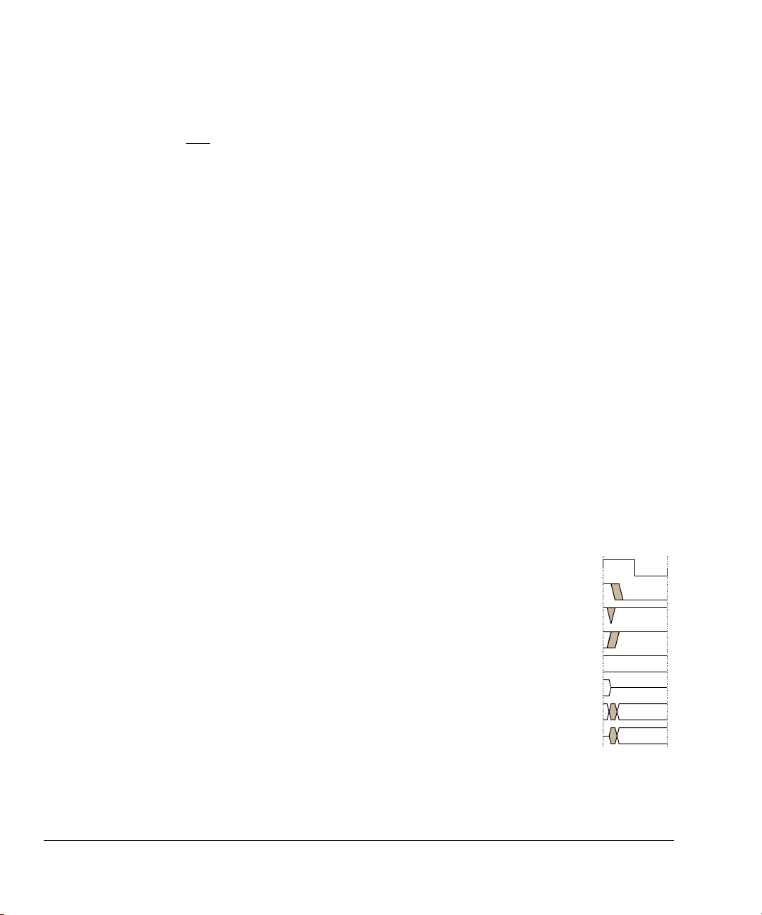
Timing diagrams
The figure named Key to timing diagram conventions explains the components used in
timing diagrams. Variations, when they occur, have clear labels. You must not assume
any timing information that is not explicit in the diagrams.
Shaded bus and signal areas are undefined, so the bus or signal can assume any value
within the shaded area at that time. The actual level is unimportant and does not affect
normal operation.
xx Copyright © 2003-2010 ARM Limited. All rights reserved. ARM DUI 0224I
Key to timing diagram conventions
Page 21

Preface
Signals
The signal conventions are:
Signal level The level of an asserted signal depends on whether the signal is
active-HIGH or active-LOW. Asserted means HIGH for
active-HIGH signals and LOW for active-LOW signals.
Lower-case n Denotes an active-LOW signal.
Prefix A Denotes global Advanced eXtensible Interface (AXI) signals:
Prefix AR Denotes AXI read address channel signals.
Prefix AW Denotes AXI write address channel signals.
Prefix B Denotes AXI write response channel signals.
Prefix C Denotes AXI low-power interface signals.
Prefix H Denotes Advanced High-performance Bus (AHB) signals.
Prefix P Denotes Advanced Peripheral Bus (APB) signals.
Prefix R Denotes AXI read data channel signals.
Prefix W Denotes AXI write data channel signals.
Numbering
The numbering convention is:
<size in bits>'<base><number>
This is a Verilog method of abbreviating constant numbers. For example:
• 'h7B4 is an unsized hexadecimal value.
• 'o7654 is an unsized octal value.
• 8'd9 is an eight-bit wide decimal value of 9.
• 8'h3F is an eight-bit wide hexadecimal value of
0x3F
. This is
equivalent to b00111111.
• 8'b1111 is an eight-bit wide binary value of b00001111.
ARM DUI 0224I Copyright © 2003-2010 ARM Limited. All rights reserved. xxi
Page 22

Preface
Further reading
This section lists publications by ARM Limited, and by third parties.
ARM Limited periodically provides updates and corrections to its documentation. See
http://www.arm.com
for current errata sheets, addenda, and the Frequently Asked
Questions list.
ARM publications
This manual contains information that is specific to the PB926EJ-S Platform
Baseboard. See the following documents for other relevant information:
The following publications provide information about the registers and interfaces on the
ARM926EJ-S PXP Development Chip:
• ARM926EJ-S Development Chip Reference Guide (ARM DDI 0287)
• ARM926EJ-S Technical Reference Manual (ARM DDI 0198)
• ARM926EJ-S
™
PrimeXsys Platform Virtual Component Technical Reference
Manual (ARM DDI 0232)
™
• ARM926EJ-S
PrimeXsys Platform Virtual Component User Guide
(ARM DUI 0213)
• ARM MOVE Coprocessor Technical Reference Manual (ARM DDI 0251)
• ARM VFP9-S Coprocessor Technical Reference Manual (ARM DDI 0238)
• ARM MBX HR-S Graphics Core Technical Reference Manual (ARM DDI 0241).
The following publications provide reference information about the ARM architecture:
• AMBA
™
Specification (ARM IHI 0011)
• ARM Architecture Reference Manual (ARM DDI 0100).
The following publications provide information about related ARM products and
toolkits:
• Multi-ICE
• RealView
™
User Guide (ARM DUI 0048)
™
ICE User Guide (ARM DUI 0155)
• Trace Debug Tools User Guide (ARM DUI 0118)
®
• ARM MultiTrace
User Guide (ARM DUI 0150)
• ARM RealView Logic Tile LT-XC2V4000+ User Guide (ARM DUI 0186)
™
• RealView
Debugger User Guide (ARM DUI 0153)
• RealView Compilation Tools Compilers and Libraries Guide (ARM DUI 0205)
• RealView Compilation Tools Developer Guide (ARM DUI 0203)
• RealView Compilation Tools Linker and Utilities Guide (ARM DUI 0206).
xxii Copyright © 2003-2010 ARM Limited. All rights reserved. ARM DUI 0224I
Page 23

Preface
The following publications provide information about ARM PrimeCell® and other
peripheral or controller devices:
• ARM PrimeCell Advanced Audio CODEC Interface (PL041) Technical Reference
Manual (ARM DDI 0173)
• ARM PrimeCell Color LCD Controller (PL110) Technical Reference Manual
(ARM DDI 0161)
• ARM PrimeCell DMA (PL080) Technical Reference Manual (ARM DDI 0196)
• ARM Dual-Timer Module (SP804) Technical Reference Manual
(ARM DDI 0271)
• ARM PrimeCell GPIO (PL061) Technical Reference Manual (ARM DDI 0190)
• ARM PrimeCell Keyboard Mouse Controller (PL050) Technical Reference
Manual (ARM DDI 0143)
• ARM PrimeCell Multimedia Card Interface (PL180) Technical Reference Manual
(ARM DDI 0172)
• ARM Multiport Memory Controller (GX175) Technical Reference Manual
(ARM DDI 0277)
• ARM PrimeCell Real Time Clock Controller (PL031) Technical Reference
Manual (ARM DDI 0224)
• ARM PrimeCell Smart Card Interface (PL131) Technical Reference Manual
(ARM DDI 0228)
• ARM PrimeCell Synchronous Serial Port Controller (PL022) Technical Reference
Manual (ARM DDI 0194)
• ARM PrimeCell Synchronous Static Memory Controller (PL093) Technical
Reference Manual (ARM DDI 236)
• ARM PrimeCell System Controller (SP810) Technical Reference Manual
(ARM DDI 0254)
• ARM PrimeCell UART (PL011) Technical Reference Manual (ARM DDI 0183)
• ARM PrimeCell Vector Interrupt Controller (PL190) Technical Reference
Manual (ARM DDI 0181)
• ARM PrimeCell Watchdog Controller (SP805) Technical Reference Manual
(ARM DDI 0270)
• ETM9 Technical Reference Manual (ARM DDI 0157).
ARM DUI 0224I Copyright © 2003-2010 ARM Limited. All rights reserved. xxiii
Page 24

Preface
Other publications
This section lists relevant documents published by third parties:
The following publication describes the JTAG ports with which Multi-ICE or RealView
ICE communicates:
• IEEE Standard Test Access Port and Boundary Scan Architecture (IEEE Std.
1149.1).
The following datasheets describe some of the integrated circuits or modules used on
the PB926EJ-S:
• CODEC with Sample Rate Conversion and 3D Sound (LM4549) National
Semiconductor, Santa Clara, CA.
• Mobile DiskOnChip Plus 32/64MByte, M-Systems Inc., Newark, CA.
• MultiMedia Card Product Manual SanDisk, Sunnyvale, CA.
• Serially Programmable Clock Source (ICS307), ICS, San Jose, CA.
• Serial Microwire Bus EEPROM (M93LC46) STMicroelectronics, Amsterdam,
The Netherlands.
• 1.8 Volt Intel StrataFlash
®
Wireless Memory with 3.0 Volt I/O Intel Corporation,
Santa Clara, CA. See the Build of Materials (BOM) file for the part number of the
flash device.
• TFT-LCD Module (LQ084V1DG21) Sharp Corporation, Osaka, Japan.
• Three-In-One Fast Ethernet Controller (LAN91C111) SMSC, Hauppauge, NY.
• Touch Screen Controller (TCS2200) Texas Instruments, Dallas, TX.
xxiv Copyright © 2003-2010 ARM Limited. All rights reserved. ARM DUI 0224I
Page 25

Feedback
ARM®Limited welcomes feedback both on the PB926EJ-S and on the documentation.
Feedback on this product
If you have any comments or suggestions about this product, contact your supplier
giving:
• the product name
• a concise explanation of your comments.
Feedback on this manual
Preface
If you have any comments about this document, send email to
errata@arm.com
• the title
• the number
• the relevant page number(s) to which your comments apply
• a concise explanation of your comments.
®
ARM
Limited also welcomes general suggestions for additions and improvements.
giving:
ARM DUI 0224I Copyright © 2003-2010 ARM Limited. All rights reserved. xxv
Page 26

Preface
xxvi Copyright © 2003-2010 ARM Limited. All rights reserved. ARM DUI 0224I
Page 27

Chapter 1
Introduction
This chapter introduces the PB926EJ-S. It contains the following sections:
• About the PB926EJ-S on page 1-2
• PB926EJ-S architecture on page 1-4
• Precautions on page 1-9.
ARM DUI 0224I Copyright © 2003-2010 ARM Limited. All rights reserved. 1-1
Page 28

Introduction
1.1 About the PB926EJ-S
The PB926EJ-S provides a development system that you can use to develop products
around the ARM926EJ-S PXP Development Chip.
You can use the PB926EJ-S as a basic development system with a power supply and a
connection to a JTAG interface unit.
You can expand the PB926EJ-S by adding:
• ARM RealView Logic Tiles containing custom IP
• a PCI expansion enclosure
• Dynamic memory expansion board
• Static memory expansion board
• VGA monitor or CLCD adaptor and CLCD display
• MMC, SD, or SIM cards
• custom devices to the 32-bit GPIO
• USB devices to the three USB ports
• serial devices to the synchronous serial port and the four UARTs
• keyboard and mouse
• audio devices to the onboard CODEC
• an Ethernet network to the onboard Ethernet controller.
The basic system provides a good platform for developing code for the ARM7 and
ARM9 series of processors. The ARM926EJ-S PXP Development Chip is much faster
than a software simulator or a core implemented in RealView Logic Tiles. Code
developed for the ARM926EJ-S PXP Development Chip will also run on the ARM10
and ARM11 processor series.
The expanded system with RealView Logic Tiles can be used to develop
AMBA-compatible peripherals and to test ASIC designs. The fast processor core and
the peripherals present in the ARM926EJ-S PXP Development Chip, PB926EJ-S
FPGA, and RealView Logic Tile FPGA enable you to develop and text complex
systems operating at, or near, their target operating frequency.
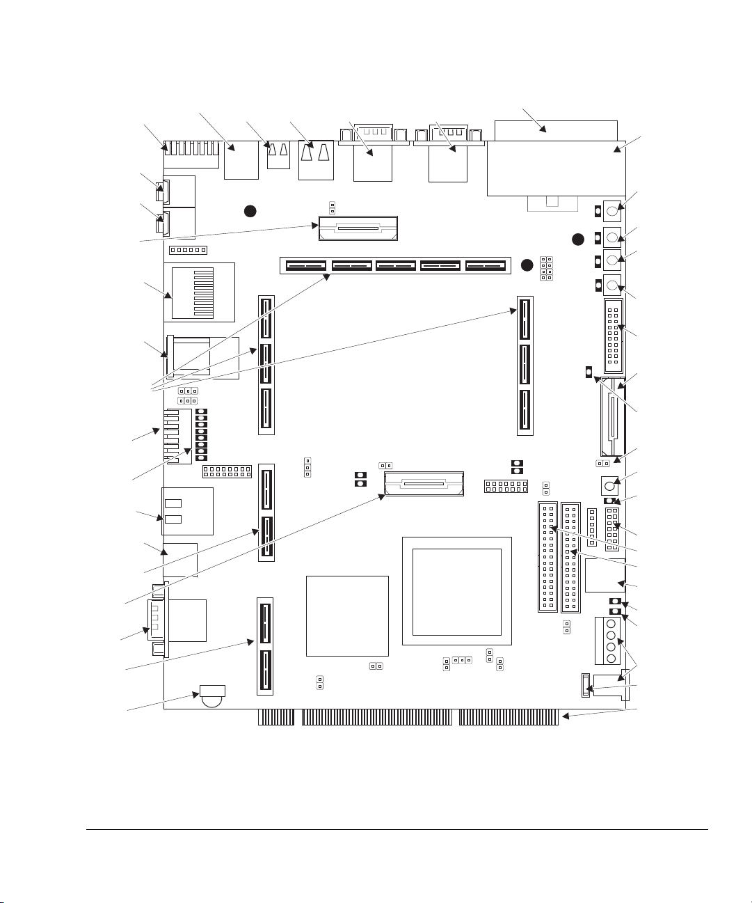
Figure 1-1 on page 1-3 shows the layout of the PB926EJ-S.
1-2 Copyright © 2003-2010 ARM Limited. All rights reserved. ARM DUI 0224I
Page 29
Introduction
GP
(user)
LEDs
S6 GP
(user)
switches
Power LED
(red)
Power
S1
configuration
switches
Fuse
CONFIG
link
L
ine in
(bottom)
ine out
(top)
L
Mic in
MMC
0 (top)
1 (bottom)
Smart
card
0 (top)
1 (bottom)
Ethernet
Keyboard
VGA
Battery
PCI
expansion
USB debug
USB
0 (top)
1 (bottom)
UART
0 (top)
1 (bottom)
OTG
USB
Mouse
CLCD expansion
connector
JTAG
Trace
port
Dynamic
memory
expansion
2X16
character
LCD
ARM926EJ-S
Development
Chip
FPGA
GPIO 0,1
Logic Tile
expansion
GPIO 2,3
UART
2 (top)
3 (bottom)
ChipScope
0
1
Static
memory
expansion
CFGEN LED
(orange)
GP PUSH
(green LED)
DEV CHIP
CONFIG
(blue LED)
FPGA
CONFIG
(yellow LED)
RESET
(orange LED)
0
FPGA
debug
AHB
monitor
3V3 OK
(green LED)
5V OK
(green LED)
Standby/
power
Figure 1-1 PB926EJ-S layout
ARM DUI 0224I Copyright © 2003-2010 ARM Limited. All rights reserved. 1-3
Page 30

Introduction
1.2 PB926EJ-S architecture
The major components on the platform are:
• ARM926EJ-S PXP Development Chip equipped with:
— ARM926EJ-S processor that supports 32-bit ARM and 16-bit Thumb
instructions sets and includes features for direct execution of Java byte
codes. Executing Java byte codes requires the Java Technology Enabling
Kit (JTEK)
— Tightly-Coupled Memory (TCM) for code (32KB) and data (32KB)
— cache memory for code (32KB) and data (32KB)
— Memory Management Unit (MMU)
— Multi-layer bus matrix that gives highly efficient simultaneous transfers
—MOVE
— MBX graphics accelerator
— Multi-Port Memory Controller (MPMC) for direct connection to dynamic
memory
— Synchronous Static Memory Controller (SSMC) for direct connection to
static (SRAM or flash) memory
— VFP9 Vector Floating Point coprocessor
— two external AHB master bridges and one external AHB slave bridge
— AHB monitor for detailed analysis of bus activity
— System Controller
— DMA controller
— Vectored Interrupt Controller (VIC)
— Color LCD controller (CLCDC)
— Three UARTs,
— Synchronous Serial Port (SSP)
— Smart Card Interface (SCI)
— Four eight-bit GPIOs
— Real Time Clock (RTC)
— Two programmable timers
— Watchdog timer
— Embedded Trace Macrocell (ETM9)
— Embedded-ICE logic for JTAG debugging
— Phase-Locked Loop (PLL)
— Configuration Block.
™
video encoding coprocessor
1-4 Copyright © 2003-2010 ARM Limited. All rights reserved. ARM DUI 0224I
Page 31

Introduction
• Field Programmable Gate-Array (FPGA) that implements:
— SSP, Smart Card, two MMC/SD card, UART, and two KMI controllers
— configuration registers
— interface to onboard Ethernet controllers
— interface to onboard audio CODEC
— interface to onboard On-the-Go (OTG) USB controller (three connectors)
— registers for status, ID, onboard switches, LEDs, and clock control
— a secondary interrupt controller and external DMA control logic
— interface to PCI bus (for expansion through optional PCI expansion
enclosure).
• 128MB of 32-bit wide SDRAM
• 2MB of 32-bit wide static RAM
• 128MB of 32-bit wide NOR flash (two devices)
• up to 320MB of static memory in an optional static memory expansion board
• up to 256MB of SDRAM in an optional dynamic memory expansion board
• programmable clock generators
• connectors for VGA, color LCD display interface board, PCI, UART, GPIO,
keyboard, mouse, Smart Card, USB, audio, MMC, SSP, and Ethernet
• RealView Logic Tile connector (one or more optional RealView Logic Tiles can
be used to develop custom IP)
• debug and test connectors for JTAG, AHB monitor, ChipScope, and Trace port
• DIP switches and LEDs
• 2 row by 16 character LCD display
• power conversion circuitry
• Real-Time Clock (RTC)
• time of year clock with backup battery.
ARM DUI 0224I Copyright © 2003-2010 ARM Limited. All rights reserved. 1-5
Page 32

Introduction
MCIKMI
AACI
SCI
Interrupt
controller
3 x
UARTs
RTC
Timers
User
switches
Ethernet
Audio
Codec
LAN
91C911
Ethernet
User
LEDs
FPGA
ARM926EJ-S Dev. Chip
Multi-layer AHB and bus switch
CLCD
expansion
connector
OTG243
USB
2x16 char
LCD
display
VGA
DAC and
PAL
KMI
Serial
bus
Sec. interrupt
controller
DMA
expansion
I/O
LCD
SCI PCIUART USB
Control
registers
Clocks, reset, JTAG, configuration,
and control circuitry
Memory
expansion
connector
SDRAM
Flash
SRAM
Memory
expansion
connector
MUX
SSMC MPMC MBX
AHB bridges
CLCDC
32-bit
GPIO
SSP
Watch
dog
AHB bus
monitor
System
controller
DMAC
Trace Port
Adaptor
ARM 926EJ-S,
VFP9, and MOVE
USB debug
JTAG
interface
Chip scope
interface
Status
LEDs
Control
switches
JTAG
ETM9 JTAG
Realview Logic Tile
expansion connectors
(also shared connections to I/O
signals from GPIO, AHB monitor,
SCI, UART, SSP, and CLCD)
PB926EJ-S
APB
bridge
AHBM1
AHBM2
AHBS
Configuration
Keyboard
Mouse
1.2.1 System architecture
Figure 1-2 shows the architecture of the PB926EJ-S.
Figure 1-2 PB926EJ-S block diagram
1-6 Copyright © 2003-2010 ARM Limited. All rights reserved. ARM DUI 0224I
Page 33

1.2.2 ARM926EJ-S PXP Development Chip
For details on the ARM926EJ-S PXP Development Chip, see ARM926EJ-S PXP
Development Chip on page 3-3 and the ARM926EJ-S PXP Development Chip
Reference Manual.
1.2.3 PB926EJ-S FPGA
The FPGA provides system control and configuration functions for the PB926EJ-S that
enable it to operate as a standalone development system or with expansion RealView
Logic Tiles or PCI cards. See FPGA on page 3-17.
The FPGA also implements additional peripherals, for example the audio CODEC,
USB, Ethernet and PCI interfaces.
1.2.4 Displays
The ARM926EJ-S PXP Development Chip outputs signals for a color LCD display. An
external interface board can be connected to the CLCD connector to drive different size
displays.
The CLCD signals from the ARM926EJ-S PXP Development Chip are converted on the
PB926EJ-S to a VGA signal. The resolution of the VGA signal is configurable. See
Appendix C CLCD Display and Adaptor Board.
Introduction
There is also a two row by sixteen character display mounted on the PB926EJ-S. This
display can be used for debugging or as the output from applications.
1.2.5 RealView Logic Tile expansion
The ARM RealView Logic Tiles, such as the LT-XC2V6000, enable the development
of AMBA AHB and APB peripherals, or custom logic, for use with ARM cores. You
can place standard or custom peripherals in the FPGA on the RealView Logic Tile.
Three AHB buses, the static memory interface, and the DMA and interrupt signals are
brought out to the RealView Logic Tile connectors. See Appendix F RealView Logic
Tile.
ARM DUI 0224I Copyright © 2003-2010 ARM Limited. All rights reserved. 1-7
Page 34

Introduction
1.2.6 Memory
The volatile memory system includes SSRAM and SDRAM memory. You can expand
this memory by installing external static or dynamic memory expansion boards.
The nonvolatile memory system consists of 128MB of 32-bit flash. The flash is
managed by the static memory controller in the ARM926EJ-S PXP Development Chip.
You can expand the flash memory by installing an external static memory expansion
board. See Appendix E Memory Expansion Boards.
1.2.7 Clock generators
The PB926EJ-S contains the following clock sources:
• crystal oscillators (these are the reference frequencies for the Real Time Clock,
• five programmable ICS307 clock sources. Two of these are used as the reference
• if fitted, the PCI backplane or RealView Logic Tiles. The external clocks can be
USB, AACI, Ethernet, and programmable oscillators)
for the CPU system clock in the ARM926EJ-S PXP Development Chip and the
CLCD controller clock. The other three programmable clocks can be used as
external reference clocks for the AHB buses.
selected as the reference clocks for the PB926EJ-S.
See Clock architecture on page 3-35.
1.2.8 Debug and test interfaces
The JTAG connector enables JTAG hardware debugging equipment, such as Multi-ICE
or RealView ICE, to be connected to the PB926EJ-S. The JTAG signals can also be
controlled by the on-board USB debug port controller. See JTAG and USB debug port
support on page 3-96.
A Mictor connector on the PB926EJ-S enables monitoring of the ARM926EJ-S PXP
Development Chip Embedded Trace Macrocell (ETM9) signals by a Trace Port
Analyzer (TPA). The trace port is medium trace size (16-bit packet). See Trace
connector pinout on page A-37 for connection information.
1-8 Copyright © 2003-2010 ARM Limited. All rights reserved. ARM DUI 0224I
Page 35

1.3 Precautions
Warning
Caution
Caution
This section contains safety information and advice on how to avoid damage to the
PB926EJ-S.
1.3.1 Ensuring safety
The PB926EJ-S can be powered from one of the following sources:
• the supplied power supply connected to J35
• a bench power supply connected to the screw terminals on header J34
•an external PCI bus.
Do not supply more than one power source. If you are using the baseboard with the PCI
enclosure for example, do not connect a power source to J35 or J34.
To avoid a safety hazard, only connect Safety Extra Low Voltage (SELV) equipment to
the connectors on the PB926EJ-S.
1.3.2 Preventing damage
Introduction
The PB926EJ-S is intended for use in a laboratory or engineering development
environment. If operated without an enclosure, the board is sensitive to electrostatic
discharges and generates electromagnetic emissions.
To avoid damage to the board, observe the following precautions.
• never subject the board to high electrostatic potentials
• always wear a grounding strap when handling the board
• only hold the board by the edges
• avoid touching the component pins or any other metallic element
• do not connect more than one power source to the platform
• always power down the board when connecting RealView Logic Tiles or
expansion boards.
Do not use the board near equipment that is:
• sensitive to electromagnetic emissions (such as medical equipment)
• a transmitter of electromagnetic emissions.
ARM DUI 0224I Copyright © 2003-2010 ARM Limited. All rights reserved. 1-9
Page 36

Introduction
1-10 Copyright © 2003-2010 ARM Limited. All rights reserved. ARM DUI 0224I
Page 37

Chapter 2
Getting Started
This chapter describes how to set up and prepare the PB926EJ-S for use. It contains the
following sections:
• Setting up the RealView Platform on page 2-2
• Setting the configuration switches on page 2-3
• Connecting JTAG debugging equipment on page 2-8
• Connecting the Trace Port Analyzer on page 2-10
• Supplying power on page 2-13
• Using the PB926EJ-S Boot Monitor and platform library on page 2-14.
ARM DUI 0224I Copyright © 2003-2010 ARM Limited. All rights reserved. 2-1
Page 38

Getting Started
Note
2.1 Setting up the RealView Platform
The following items are supplied with the PB926EJ-S:
• the PB926EJ-S printed-circuit board mounted on a metal tray
• an AC power supply that provides a 12VDC output
• a CD containing sample programs, Boot Monitor code, FPGA and PLD images,
and additional documentation
• this user guide.
To set up the PB926EJ-S as a standalone development system:
1. Set the configuration switches to select the boot memory location, operating
frequency, and FPGA image. See Setting the configuration switches on page 2-3.
2. If you are using memory expansion boards, connect them to the PB926EJ-S. See
Appendix E Memory Expansion Boards.
3. If you are using an external display:
• For VGA displays, connect the cable from the display to the VGA
connector on the PB926EJ-S.
• For CLCD displays, connect the CLCD adaptor board cable to the
PB926EJ-S. See Appendix C CLCD Display and Adaptor Board.
4. If you are using expansion Logic Tiles, mount the tile on the tile expansion
connectors. See Appendix F RealView Logic Tile and the manual for your Logic
Tile.
5. If you are using a Trace Port Analyzer (TPA), connect the Trace Port interface
buffer board. See Connecting the Trace Port Analyzer on page 2-10.
6. If you are using a debugger, connect to the JTAG or USB debug port on the board.
See Connecting JTAG debugging equipment on page 2-8.
7. Apply power to the PB926EJ-S. See Supplying power on page 2-13.
8. If you are using the supplied Boot Monitor software to select and run an
application, see Using the PB926EJ-S Boot Monitor and platform library on
page 2-14
If you are using the PB926EJ-S with the PCI backplane, see also Appendix D PCI
Backplane and Enclosure.
2-2 Copyright © 2003-2010 ARM Limited. All rights reserved. ARM DUI 0224I
Page 39

2.2 Setting the configuration switches
Note
Configuration switches S1 and S6, shown in Figure 2-1, control how the PB926EJ-S
configures itself and the action to take after reset.
Getting Started
Figure 2-1 Location of S1-1 and S6-1
2.2.1 Boot memory configuration
The configuration switches S1-1 to S1-8 determine boot memory type, the FPGA
image, and the Logic Tile image, memory configuration, and FPGA options at power
on.
Use switch S1-1 and S1-2 to select the boot device as shown in Table 2-1 on page 2-4.
If the switch lever is down, the switch is ON. The default is OFF, switch lever up.
ARM DUI 0224I Copyright © 2003-2010 ARM Limited. All rights reserved. 2-3
Page 40

Getting Started
Note
Table 2-1 Selecting the boot device
S1-2 S1-1 Device
OFF OFF Reserved (boot from NOR flash 2 - default setting)
OFF ON NOR flash 1, see Booting from NOR flash 1 on page 4-12
ON OFF Reserved
ON ON AHB expansion memory, see Booting from AHB expansion memory on page 4-14
Configuration switches S1-1 to S1-8 are not normally changed from their factory
default positions listed in Table 2-2. For more information on configuration switch S1,
see Configuration control on page 3-7.
Table 2-2 Default switch positions
Switch Default Function in default position
S1-1 and S1-2 OFF Selects NOR flash 2 as boot memory
S1-3 OFF Selects synchronous AHB bridge mode.
S1-4 OFF Reserved (SSMC enabled), leave in OFF position
S1-5 OFF Selects OSCCLK frequency of 35MHz.
S1-6 and S1-7 OFF Selects PB926EJ-S FPGA image 0
S1-8 OFF Selects Logic Tile FPGA image 0
For information on other configuration links see Test, configuration, and debug
interfaces on page 3-94. For the function of the status LEDs see LED Indicators on
page 2-5,
2-4 Copyright © 2003-2010 ARM Limited. All rights reserved. ARM DUI 0224I
Page 41

2.2.2 LED indicators
Table 2-3 lists the PB926EJ-S LED indicators and their function.
LED ID Color Device Function
5V OK Green D29 Indicates that the 5V power supply is on
3V3 OK Green D34 Indicates that the 3V3 power supply is on
Standby Red D39 Indicates that the PB926EJ-S is in standby mode and the
Config Amber D44 Indicates that the PB926EJ-S is in configuration mode.
Getting Started
Table 2-3 LED Indicators
power is off. This LED only functions when power is
supplied to the board via connector J35
Configuration mode is entered by fitting the CONFIG
link J32 on the board and powering-up
The CONFIG link is a switch on some board versions.
FPGA
Config
DEV CHIP
Reconfig
Yellow D6 Directly indicates the status of the FPGA Config
pushswitch S4. LED is off when the switch is pressed
Blue D3 Directly indicates the status of the DEV CHIP Reconfig
pushswitch S5. LED is off when the switch is pressed
Reset Amber D4 Directly indicates the status of the Reset pushswitch S2.
LED is off when the switch is pressed
GP (User)
Pushswitch
GP (User)
LEDs
Green D5 Directly indicates the status of the general purpose
pushswitch S3. LED is off when the switch is pressed
Green D12-18,
D20
Eight general purpose LEDs. These LEDs are controlled
individually by the lower eight bits of the SYS_LED
register. See User switches and LEDs on page 3-87 for
further details
Ethernet Green
Ye ll o w
J5 Ethernet activity indicators. These LEDs are integral to
the Ethernet connector J5 and are configured by writing
to a register in the LAN91C111 fast Ethernet controller.
See Ethernet interface on page 3-68 for further details
Global
Done
Green D8 Indicates that all the FPGA devices on the Logic Tiles
have been configured
ARM DUI 0224I Copyright © 2003-2010 ARM Limited. All rights reserved. 2-5
Page 42

Getting Started
Table 2-3 LED Indicators (continued)
LED ID Color Device Function
Local
Done
USB Debug
Busy
Green D7 Indicates that the PB926EJ-S FPGA device has been
configured
Amber D22 Indicates that the embedded Real View ICE Micro
Edition hardware is active
USB DebugOnGreen D23 Indicates that the embedded RealView ICE Micro
Edition hardware is enabled
2-6 Copyright © 2003-2010 ARM Limited. All rights reserved. ARM DUI 0224I
Page 43

2.2.3 Boot Monitor configuration
Note
Switches S6-1 and S6-3 control the Boot Monitor.
The setting of S6-1 determines whether the Boot Monitor starts after a reset:
S6-1 OFF A prompt is displayed enabling you to enter Boot Monitor commands.
S6-1 ON The Boot Monitor executes a boot script that has been loaded into flash.
The boot script can execute any Boot Monitor commands. It typically
selects and runs an image in application flash. You can store one or more
code images in flash memory and use the boot script to start an image at
reset. Use the
Boot Monitor (see Table 2-4 on page 2-15).
Output of text from STDIO for both applications and Boot Monitor I/O depends on the
setting of S6-3:
S6-3 ON STDIO is redirected to UART0. This occurs even under semihosting.
S6-3 OFF STDIO autodetects whether to use semihosting I/O or a UART. If a
debugger is connected and semihosting is enabled, STDIO is redirected
to the debugger console window. Otherwise, STDIO goes to the UART.
S6-3 does not affect file I/O operations performed under semihosting. Semihosting
operation requires a debugger and a JTAG interface device. See Redirecting character
output to hardware devices on page 2-21 for more details on I/O.
SET BOOTSCRIPT
Getting Started
command to enter a boot script from the
Switch S6-2 and S6-4 to S6-8 are not used by the Boot Monitor and are available for
user applications.
ARM DUI 0224I Copyright © 2003-2010 ARM Limited. All rights reserved. 2-7
Page 44

Getting Started
2.3 Connecting JTAG debugging equipment
You can use JTAG debugging equipment and the JTAG connector, or the USB debug
port, to:
• connect a debugger to the ARM926EJ-S core and download programs to memory
and debug them
• program new configuration images into the configuration flash, FPGA, and PLDs
on the board. (You cannot program the normal flash from configuration mode.)
The setup for using a JTAG interface with the PB926EJ-S is shown in Figure 2-2.
Figure 2-2 JTAG connection
The setup for using the USB debug port on the PB926EJ-S is shown in Figure 2-3 on
page 2-9. The PB926EJ-S contains logic that interfaces the USB debug port to the
onboard JTAG signals.
2-8 Copyright © 2003-2010 ARM Limited. All rights reserved. ARM DUI 0224I
Page 45

Getting Started
Note
Figure 2-3 USB debug port connection
For more details on JTAG debugging and selection between the JTAG and USB debug
connector, see JTAG and USB debug port support on page 3-96. If you are using the
®
ARM RealView
Debugger, see Appendix G Configuring the USB Debug Connection
for installation and configuration details.
ARM DUI 0224I Copyright © 2003-2010 ARM Limited. All rights reserved. 2-9
Page 46

Getting Started
2.4 Connecting the Trace Port Analyzer
The ARM926EJ-S PXP Development Chip incorporates an ARM9 Embedded Trace
Macrocell (ETM9). This enables you to carry out real-time debugging by connecting
external trace equipment to the PB926EJ-S. The ETM9 monitors the program execution
and sends a compressed trace to the Trace Port Analyzer (TPA). The TPA buffers this
information and transmits it to the debugger where it is decompressed and used to
reconstruct the complete instruction flow. The trace size is medium (16-bit packets).
For MultiTrace, connect the TPA to the buffer board and plug the adaptor into the
PB926EJ-S as shown in Figure 2-4. MultiTrace requires a Multi-ICE JTAG unit.
Figure 2-4 Example of MultiTrace and JTAG connection
For RealView Trace, connect the Trace Port Analyzer (TPA) to the adaptor board and
plug the adaptor into the PB926EJ-S as shown in Figure 2-4. RealView Trace requires
a RealView ICE JTAG unit. The Ethernet and power supply cables connect to the
RealView ICE unit.
2-10 Copyright © 2003-2010 ARM Limited. All rights reserved. ARM DUI 0224I
Page 47

Getting Started
Note
Figure 2-5 Example of RealView ICE and RealView Trace
The high-density cable from the RealView ICE box requires a buffer board to connect
to the JTAG connector on the PB926EJ-S.
The low-density cable can be used to connect the RealView ICE box directly to the
JTAG connector, but this interface operates at lower speed.
ARM DUI 0224I Copyright © 2003-2010 ARM Limited. All rights reserved. 2-11
Page 48

Getting Started
Note
2.4.1 About using trace
The components used for trace capture are:
ETM The Embedded Trace Macrocell is part of the ARM926EJ-S PXP
Trace connector and adaptor board
JTAG unit This is a protocol converter that converts debug commands from the
Trace Port Analyzer
Development Chip. It monitors the ARM core buses and outputs
compressed information through the trace port to a trace connector. The
on-chip ETM contains trigger and filter logic to control what is traced.
The trace connector enables you to connect a TPA to the PB926EJ-S. The
connector is a high-density AMP Mictor connector. The pinout for this
connector is provided in Test and debug connections on page A-33.
The adaptor board buffers the high-speed signals between the Trace
connector and the Trace Port Analyzer.
debugger into JTAG messages for the ETM.
The TPA is an external device (such as RealView Trace) that connects to
the trace connector (through the adaptor board) and stores information
sent from the ETM.
Debugger and Trace software
The debugger and trace software controls the JTAG, ETM, and Trace Port
Analyzer. The trace software reconstructs program flow from the
information captured in the Trace Port Analyzer.
The trace and debug components must match the debugger you are using:
ARM eXtended Debugger (AXD)
AXD is a component of the ARM Developer Suite (ADS). Use AXD with
Multi-ICE, Trace Debug Toolkit, and Multi-Trace.
ARM RealView Debugger (RVD)
RVD is a component of RealView Compilation Tools (RVCT). Use RVD
with RealView ICE and RealView Trace or with Multi-ICE and
Multi-Trace.
2-12 Copyright © 2003-2010 ARM Limited. All rights reserved. ARM DUI 0224I
Page 49

2.5 Supplying power
Note
Caution
When using the PB926EJ-S as a standalone development system, you must connect the
supplied brick power supply to power socket J35 or an external bench power supply to
the screw-terminal connector. See Figure 2-6.
Getting Started
Figure 2-6 Power connectors
If you are using the supplied brick power supply connected to J35, the Standby/power
pushbutton toggles the power on and off.
If you are using an external power supply connected to J34, or you are powering the
board from the PCI backplane, the Standby/power switch is not used and power is
controlled by shutting down the external power source.
You can use only one power source for the system. Use only the PCI connector, J34, or
J35. Do not, for example, use the PCI connector and J34 at the same time.
ARM DUI 0224I Copyright © 2003-2010 ARM Limited. All rights reserved. 2-13
Page 50

Getting Started
Note
Note
2.6 Using the PB926EJ-S Boot Monitor and platform library
The PB926EJ-S Boot Monitor is a collection of tools and utilities designed as an aid to
developing applications on thePB926EJ-S.
When the Boot Monitor starts on reset, the following actions are performed:
• clock dividers are loaded with appropriate values
• the memory controllers are initialized
• a stack is set up in memory
• Boot Monitor code is copied into SDRAM
• C library I/O routines are remapped and redirected
• the current bootscript, if any, is run.
2.6.1 Running the Boot Monitor
To run Boot Monitor and have it display a prompt to a terminal connected to UART0,
set switch S6-1 to OFF and reset the system. Standard input and output functions use
UART0 by default. The default setting for UART0 is 38400 baud, 8 data bits, no parity,
1 stop bit. There is no hardware or software flow control.
If the Boot Monitor has been accidently deleted from flash memory, it can be rebuilt and
reloaded. See Rebuilding the Boot Monitor on page 2-18.
Boot Monitor commands
The command interpreter accepts user commands from the debugger console window
or an attached terminal and carries out actions to complete the commands.
Commands are accepted in uppercase or lowercase. The Boot Monitor accepts
abbreviations of commands if the meaning is not ambiguous. For example, for
can type
2-14 Copyright © 2003-2010 ARM Limited. All rights reserved. ARM DUI 0224I
QUIT, QUI, QU, Q, quit, qui, qu, or q
.
QUIT
, you
Page 51

Table 2-4 lists the commands for the Boot Monitor.
Note
Command Action
Getting Started
Table 2-4 Boot Monitor commands
@ script_file
ALIAS alias commands
CLEAR BOOTSCRIPT
CONFIGURE
CONVERT BINARY binary_file
LOAD_ADDRESS address
[ENTRY_POINT address]
DEBUG
DISABLE CACHES
DISPLAY BOOTSCRIPT
ECHO text
ENABLE CACHES
EXIT
FLASH
Runs a script file.
Create an alias command
alias
for the string of commands contained in
commands
.
Clear the current boot script. The Boot Monitor will prompt for input on reset even if the
S6-1 is set to ON to indicate that a boot script should be run.
Enter Configure subsystem. Commands listed in Table 2-5 on page 2-16 can now be
executed.
Provides information to the system that is required by the RUN command in order to
execute a binary file. A new file with name
binary_file
is produced, but with an
.exe
file
extension.
Enter the debug subsystem. Commands listed in Table 2-6 on page 2-16 can now be
executed.
Disable both the I and D caches.
Display the current boot script.
Echo
text
to the current output device.
Enable both the I and D caches.
Exit the Boot Monitor. The processor is held in a tight loop until it is interrupted by a JTAG
debugger.
Enter the flash file system for the NOR flash on the PB926EJ-S. See Table 2-7 on
page 2-17 for flash commands.
HELP
QUIT
SET BOOTSCRIPT
script_file Specify
List the Boot Monitor commands.
Alias for
script_file
EXIT
. Exit the Boot Monitor.
script_file
as the boot script. If the run boot script switch S6-1 is ON,
will be run at system reset.
Table 2-5 on page 2-16 lists the commands for the Configure subsystem.
You must reset the board for the Boot Monitor Configure commands to take effect
ARM DUI 0224I Copyright © 2003-2010 ARM Limited. All rights reserved. 2-15
Page 52

Getting Started
Command Action
Table 2-5 Boot Monitor Configure commands
DISPLAY DATE
DISPLAY HARDWARE
DISPLAY TIME
EXIT
HELP
QUIT
Display date.
Display hardware information (for example, the FPGA revisions).
Display time.
Exit the configure commands and return to executing standard Boot Monitor commands.
List the configure commands.
Alias for
EXIT
. Exit the Configure commands and return to standard Boot Monitor
commands.
SET DATE dd/mm/yy
SET TIME hh:mm:ss
SET AHBM1
SET AHBM2
SET AHBS
Set date. The date can also be entered as
Set time. The time can also be entered as
Configures AHBM1 bridge
Configures AHBM2 bridge
Configures AHBS bridge
Table 2-6 lists the commands for the Debug subsystem.
Command Action
dd-mm-yy
hh-mm-ss
Table 2-6 Boot Monitor Debug commands
DEPOSIT address value [size]
DISABLE MESSAGES
ENABLE MESSAGES
EXAMINE address
EXIT
Load memory specified by
used, it can be
BYTE, HALFWORD
address
, or
with
value
WORD
. The default is
. The
size
parameter is optional. If
WORD
.
Disable debug messages
Enable debug messages
Examine memory at
address
Exit the debug commands and return to executing standard Boot Monitor
commands.
GO address
HELP
2-16 Copyright © 2003-2010 ARM Limited. All rights reserved. ARM DUI 0224I
Run the code starting at
List the debug commands.
address
.
Page 53

Command Action
Warning
Getting Started
Table 2-6 Boot Monitor Debug commands (continued)
QUIT
START TIMER
STOP TIMER
Table 2-7 lists the commands for the NOR Flash subsystem.
Command Action
DISPLAY IMAGE name
ERASE IMAGE name
ERASE RANGE start end
EXIT
HELP
LIST AREAS
Displays details of image
Erase an image or binary file from flash.
Erase an area of NOR flash from the
This command can erase the Boot Monitor image if it is stored in NOR flash. See Loading
Boot Monitor into NOR flash on page 2-20.
Exit the flash commands and return to executing standard Boot Monitor commands.
List the flash commands.
List areas in flash. An area is one or more contiguous blocks that have the same size and
use the same programming algorithm.
Alias for
EXIT
. Exit the Debug commands and return to standard Boot Monitor
commands.
Start a timer.
Stop the timer started with the
name
.
START TIMER
command and display the elapsed time.
Table 2-7 Boot Monitor NOR flash commands
start
address to the
end
address.
LIST IMAGES
LOAD name
QUIT
List images in flash.
Load the image
Alias for
image_name
EXIT
. Exit the NOR flash commands and return to standard Boot Monitor
into memory.
commands.
RESERVE SPACE address size
RUN name
ARM DUI 0224I Copyright © 2003-2010 ARM Limited. All rights reserved. 2-17
Reserve space in NOR flash. This space will not be used by the Boot Monitor.
the start of the area and
Load the image
size
is the size of the reserved area.
name
from flash and run it.
address
is
Page 54

Getting Started
Note
Note
Command Action
Table 2-7 Boot Monitor NOR flash commands (continued)
UNRESERVE SPACE address
Free the space starting at
Monitor.
WRITE BINARY file
[NAME new_name]
[FLASH_ADDRESS address]
[LOAD_ADDRESS address]
[ENTRY_POINT address]
Write a binary file to flash. By default, the image is identified by its file name. Use
NAME new_name
FLASH_ADDRESS address
Use
optional
LOAD_ADDRESS
and the entry point.
If an entry point is not specified, the load address is used as the entry point.
Remote file access requires semihosting. Use a debugger connection to provide
semihosting.
WRITE IMAGE file
[NAME new_name]
[FLASH_ADDRESS address]
Write an ELF image file to flash. By default, the image is identified by its file name. For
example, t:\images\boot_monitor.axf is identified as boot_monitor. Use
specify a name instead of using the default name.
FLASH_ADDRESS address
Use
is linked to run from flash, the link address is used and
Remote file access requires semihosting. Use a debugger connection to provide
semihosting.
2.6.2 Rebuilding the Boot Monitor
address
in NOR flash. This space can be used by the Boot
to specify a name instead of using the default name.
to specify where in flash the image is to be located. The
and
ENTRY_POINT
arguments enable you to specify the load address
to specify where in flash the image is to be located. If the image
address
is ignored.
NAME new_name
to
All firmware components are built using GNUmake, which is available for UNIX,
Linux and for most Windows versions. (To use GNUmake under windows Cygwin must
be installed, for more information contact Redhat.)
Because the platform library used by the Boot Monitor requires callout startup routines
support specific to RVCT, the Boot Monitor (and any application that uses the platform
library for directing STDIO) can only be rebuilt using RVCT tools.
To rebuild the Boot Monitor, set your default directory to
install_directory/Firmware/Boot_Monitor
You can specify the following build options after the
•
BIG_ENDIAN=1/0
•
THUMB=1/0
•
DEBUG=1/0
2-18 Copyright © 2003-2010 ARM Limited. All rights reserved. ARM DUI 0224I
, defining image endianness (Default 0, little endian)
, defining image state (Default 0, ARM)
, defining optimization level (Default 0, optimized code)
and type
make
from a DOS command line.
make
command:
Page 55

Getting Started
Note
•
VFP=1/0
, defines VFP support (Default 0, no VFP support).
The image must be build as a simple image. Scatter loading is not supported.
The build options define the subdirectory in the
Builds
directory that contains the
compile and link output:
<Debug>_<State>_<Endianness>_Endian + further component specific options
For example,
Release_ARM_Little_Endian
or
Debug_Thumb_Big_Endian_NoDiskOnChip
.
After rebuilding the Boot Monitor, load it into NOR flash, see Loading Boot Monitor
into NOR flash on page 2-20.
ARM DUI 0224I Copyright © 2003-2010 ARM Limited. All rights reserved. 2-19
Page 56

Getting Started
Note
2.6.3 Loading Boot Monitor into NOR flash
If the flash becomes corrupt and the board no longer runs the Boot Monitor, the Boot
Monitor must be reprogrammed into flash.
The Boot Monitor is normally located in NOR flash 2 instead of NOR flash 1. You can,
however, load the Boot Monitor into NOR flash 1 instead of NOR flash 2 if this is
requiredfor a specific application.
Because the debugger does not initialize SDRAM, the Boot Monitor image cannot be
loaded and run directly. Use the scripts in the
the board:
1. Power off the board
2. Set switch S1-1 to ON to select booting from NOR flash 1
Set switch S1-1 to OFF to select booting from NOR flash 2
Set all other S1 switches to OFF
Set all S6 switches to OFF.
BoardFiles
directory on the CD to setup
3. Connect a RealView ICE or Multi-ICE to the JTAG port or a debug cable to the
USB debug port.
4. Power on the board.
5. Connect the debugger to the target
• For ARM eXtended Debugger, from the Command Line Interface
Debug > Obey VPB926EJS_SDRAM_Init_axd.li
• For RealView Debugger:From the Debug menu → Include Commands
From File
Select VPB926EJS_SDRAM_Init_rvd.li
6. SDRAM is now initialized and the memory is remapped.
7. From the debugger, load and execute the file
Boot_Monitor.axf
8. Load the image into one of the NOR flash memories:
• To load the image to NOR flash 2, at the Boot Monitor prompt enter:
>FLASH
Flash> WRITE IMAGE path\Boot_Monitor.axf NAME boot_monitor
FLASH_ADDRESS 0x30000000
2-20 Copyright © 2003-2010 ARM Limited. All rights reserved. ARM DUI 0224I
Page 57

Getting Started
Note
where path is the directory (
C:\temp
monitor image.
• To load the image to NOR flash 1, at the Boot Monitor prompt enter:
>FLASH
Flash> WRITE IMAGE path\Boot_Monitor.axf NAME boot_monitor
FLASH_ADDRESS 0x34000000
where path is the directory (
C:\temp
monitor image.
Very long path names can cause problems with semihosting. To avoid this, move
the image to a temporary directory.
9. Loading the image into flash takes a few minutes to complete. Wait until the
prompt is displayed again before proceeding.
10. Turn the board off and then on.
Boot Monitor starts automatically.
2.6.4 Redirecting character output to hardware devices
The redirection of character I/O is carried out within the Boot Monitor platform library
routines in
retarget.c
and
boot.s
. During startup, the platform library executes a
SoftWare Interrupt instruction (SWI). If the image is being executed without a debugger
(or the debugger is not capturing semihosting calls) the value returned by this SWI is
–1, otherwise the value returned is positive. The platform library uses the return value
to determine the hardware device used for outputting from the C library I/O functions.
(Redirection is through a SWI to the debugger console or directly to a hardware device)
for example) that contains the boot
for example) that contains the boot
ARM DUI 0224I Copyright © 2003-2010 ARM Limited. All rights reserved. 2-21
Page 58

Getting Started
Supported devices for character output are:
•
:UART-0
(default destination if debugger is not capturing semihosting calls)
•
:UART-1
•
:UART-2
•
:UART-3
•
:CHARLCD
.
The STDIO calls are redirected within
of switch S6-3, see Boot Monitor configuration on page 2-7.
2.6.5 Rebuilding the platform library
All firmware components are built using GNUmake, which is available for UNIX,
Linux and for most Windows versions. (To use GNUmake under windows Cygwin must
be installed, for more information contact Redhat.)
To rebuild the platform library component, set your default directory to
install_directory/Firmware/platform
The platform library has a number of build options that can be specified with the
command:
•
BIG_ENDIAN=1/0
•
•
•
THUMB=1/0
DEBUG=1/0
VFP=1/0
, defining image state (Default 0, ARM)
, defining optimization level (Default 0, optimized)
, defines VFP support (Default 0 no VFP support).
The build options define the directory that contains the compile and link output. The
make file creates a directory called
directory contains subdirectories for the specified
Debug_ARM_Little_Endian
Builds
directory, type
retarget.c
and type
. Redirection depends on the setting
make
from a DOS command line.
, defining image endianness (Default 0, little endian)
Builds
if it is not already present. The
make
options (for example,
Builds
). To delete the objects and images for all targets and delete the
make clean all
.
make
2-22 Copyright © 2003-2010 ARM Limited. All rights reserved. ARM DUI 0224I
Page 59

2.6.6 Building an application with the platform library
Note
The platform library on the CD provides all required initialization code to bring the
PB926EJ-S up from reset. The library is used by the Boot Monitor, but it can be used
by an application independently of the other code in the Boot Monitor.
The platform library supports:
• remapping of boot memory
• SDRAM initialization
•UARTs
• Time-of-Year clock
• output to the character LCD display
• C library system calls.
To build an image that uses the I/O and memory control features present in the platform
library:
Getting Started
1. Write the application as normal. There must be a
2. Link the application against the Boot Monitor platform library file
The file
(
install_dir\software\firmware\Platform\Builds\target_build
Builds
Release_ARM_Little_Endian
Define the image entry point to be
platform.a
is in one of the target build subdirectories
subdirectory that matches your application. For example,
for ARM code.
__main
main()
and the region
routine in the application.
platform.a
.
). Choose the
__main
to be the first
section in the execution region:
-entry __main -first __main
If you are not using the
platform.a
library, you must provide your own
initialization and I/O routines.
You can also build the platform library functionality directly into your application
without building the platform code as a separate library. This might be useful, for
example, if you are using an IDE to develop your application.
See the
included on the CD. The
filelist.txt
file in the
selftest
software
directory for more details on software
directory, for example, contains source files
that can be used as a starting point for your own application.
To run the image from RAM, load the image with a debugger and execute as normal.
The image uses the procedure described in Redirecting character output to hardware
devices on page 2-21 to redirect standard I/O either to the debugger or to be handled by
the application itself.
ARM DUI 0224I Copyright © 2003-2010 ARM Limited. All rights reserved. 2-23
Page 60

Getting Started
Note
2.6.7 Loading and running an application from NOR flash
To run an image from NOR flash:
1. Build the application as described in Building an application with the platform
library on page 2-23 and specify a link address suitable for flash. There are the
following options for selecting the address:
Load region in flash
The image is linked such that its load region, though not necessarily its
execution region, is in flash. The load region specified when the image
was linked is used as the location in flash and the FLASH_ADDRESS
option is ignored. If the blocks in flash are not free, the command fails.
Use the
FLASH RUN
command to run the image.
Load region not in flash and image location not specified
The image is programmed into the first available contiguous set of
blocks in flash that is large enough to hold the image. Use the
LOAD
and then the
FLASH RUN
Load region not in flash, but image stored at a specified flash address
Use the FLASH_ADDRESS option to specify the location of the
image in flash. If the option is not used, the image is programmed into
the first available contiguous set of blocks in flash that is large enough
to hold the image. Use the
FLASH LOAD
and run the image.
FLASH
commands to load and run the image.
or
FLASH RUN
commands to load
Images with multiple load regions are not supported.
If the image is loaded into flash, but the
FLASH RUN
command relocates code to
SDRAM for execution, the execution address must not be in the top 4MBytes of
SDRAM since this is used by the Boot Monitor.
2. The image must be programmed into flash using the Boot Monitor. Flash support
is implemented in the Boot Monitor image.
Run the Boot Monitor image from the debugger and enter the flash subsystem,
type
FLASH
at the prompt:
>FLASH
flash>
2-24 Copyright © 2003-2010 ARM Limited. All rights reserved. ARM DUI 0224I
Page 61

3. The command used to program the image depends on the type of image:
Note
• To program the ELF image into flash, use the following command line:
flash> WRITE IMAGE elf_file_name NAME name FLASH_ADDRESS address
The entry point and load address for ELF images are taken from the image
itself.
• To program a binary image into flash, use the following command line:
flash> WRITE BINARY image_file_name NAME name FLASH_ADDRESS address1
LOAD_ADDRESS address2 ENTRY_POINT address3
flash>
name
is a short name for the image. If the
prompt,
name
will be derived from the file name.
4. The image is now in flash and can be run by the Boot Monitor. At the prompt,
type:
flash> RUN name
2.6.8 Using a boot script to run an image automatically
Use a boot script to run an image automatically after power-on:
Getting Started
NAME
option is not used at the command
1. Create a boot script from the Boot Monitor by typing:
> CREATE myscript.txt
; put any startup code here FLASH RUN file_name
2. Press Ctrl-Z to indicate the end of the boot script and return to the Boot Monitor
prompt.
3. Verify the file was entered correctly by typing:
>TYPE myscript.txt
The contents of the file is displayed to the currently selected output device.
4. Specify the boot script to use at reset from the Boot Monitor by typing:
>SET BOOTSCRIPT myscript.txt
5. Set S6-1 ON to instruct the Boot Monitor to run the boot script at power on.
6. Reset the platform. The Boot Monitor runs and executes the boot script
myscript.txt
ARM DUI 0224I Copyright © 2003-2010 ARM Limited. All rights reserved. 2-25
. In this case, it relocates the image
file_name
and executes it.
Page 62

Getting Started
2-26 Copyright © 2003-2010 ARM Limited. All rights reserved. ARM DUI 0224I
Page 63

Chapter 3
Hardware Description
This chapter describes the on-board hardware. It contains the following sections:
• ARM926EJ-S PXP Development Chip on page 3-3
• FPGA on page 3-17
• Reset controller on page 3-22
• Power supply control on page 3-33
• Clock architecture on page 3-35
• Advanced Audio Codec Interface, AACI on page 3-56
• Character LCD controller on page 3-59
• CLCDC interface on page 3-61
• DMA on page 3-65
• Ethernet interface on page 3-68
• GPIO interface on page 3-71
• Interrupts on page 3-72
• Keyboard/Mouse Interface, KMI on page 3-74
• Memory Card Interface, MCI on page 3-75
• PCI interface on page 3-79
• Serial bus interface on page 3-80
• Smart Card interface, SCI on page 3-81
ARM DUI 0224I Copyright © 2003-2010 ARM Limited. All rights reserved. 3-1
Page 64

Hardware Description
• Synchronous Serial Port, SSP on page 3-84
• User switches and LEDs on page 3-87
• USB interface on page 3-92
• UART interface on page 3-88
• Test, configuration, and debug interfaces on page 3-94.
3-2 Copyright © 2003-2010 ARM Limited. All rights reserved. ARM DUI 0224I
Page 65

3.1 ARM926EJ-S PXP Development Chip
The ARM926EJ-S PXP Development Chip and its interfaces are described in the
following sections:
• ARM926EJ-S PXP Development Chip overview
• Configuration control on page 3-7
• AHB bridges and the bus matrix on page 3-10
• AHB monitor on page 3-16
• ARM926EJ-S PXP Development Chip clocks on page 3-39
• DMA on page 3-65
• Memory interface on page 3-15
• Reset controller on page 3-22
• CLCDC interface on page 3-61
• GPIO interface on page 3-71
• UART interface on page 3-88
• Smart Card interface, SCI on page 3-81
• Synchronous Serial Port, SSP on page 3-84.
For more detail on using the ARM926EJ-S PXP Development Chip components, see
also:
• the ARM926EJ-S Development Chip Reference Manual
• AHB buses used by the FPGA and RealView Logic Tiles on page F-11
• Chapter 4 Programmer’s Reference.
Hardware Description
3.1.1 ARM926EJ-S PXP Development Chip overview
Figure 3-1 on page 3-4 shows the main blocks of the ARM926EJ-S PXP Development
Chip.
ARM DUI 0224I Copyright © 2003-2010 ARM Limited. All rights reserved. 3-3
Page 66

Hardware Description
Figure 3-1 ARM926EJ-S PXP Development Chip block diagram
3-4 Copyright © 2003-2010 ARM Limited. All rights reserved. ARM DUI 0224I
Page 67

Hardware Description
The ARM926EJ-S PXP Development Chip incorporates the following features:
ARM926EJ-S
®
The ARM926EJ-S CPU is a member of the ARM9 Thumb
family. The
ARM926EJ-S (r0p3) macrocell is a 32-bit cached processor with
ARMv5TE architecture that supports the ARM and Thumb instruction
sets and includes features for direct execution of Java byte codes.
Executing Java byte codes requires the Java Technology Enabling Kit
(JTEK).
The ARM926EJ-S contains a Memory Management Unit (MMU), 32KB
data and instruction caches, and 32KB of data and instruction Tightly
Coupled Memory (TCM). The TCM operates with a single wait-state and
provides higher data rates than external memory.
ETM9 The Embedded Trace Macrocell (ETM) provides signals for off-chip
trace. The ETM transmits a 16-bit packet to an external trace port
analyzer where the signals can be stored and later analyzed to reconstruct
the code flow.
VFP9 This high-performance, low-power Vector Floating-Point (VFP)
coprocessor implements the VFPv2 vector floating-point architecture.
MOVE The MOVE coprocessor is a video encoding accelerator designed to
accelerate Motion Estimation (ME) algorithms within block-based video
encoding schemes such as MPEG4 and H.263. For more information on
the MOVE coprocessor, see the ARM MOVE Coprocessor Technical
Reference Manual.
MBX This high-performance graphic accelerator operates on 3D scene data (as
batches of triangles) sent from the main processor. Triangles are written
directly to a tile accelerator so that the CPU is not stalled during
processing. For more information on the MBX coprocessor, see the ARM
MBX HR-S Graphics Core Technical Reference Manual.
Clock control
The ARM926EJ-S PXP Development Chip contains deskew PLL that
uses an external reference clock to generate internal clocks for the CPU,
AHB bus, memory, and off-chip peripherals. Dividers in the chip are
programmable and give considerable flexibility in clock rates for the
CPU, bridges, and memory.
AHB buses The ARM926EJ-S processor uses two separate AHB masters for
instructions and data to maximize system speed. The DMA controller has
two AHB masters. The CLCD controller has one AHB master.
ARM DUI 0224I Copyright © 2003-2010 ARM Limited. All rights reserved. 3-5
Page 68

Hardware Description
There are also two expansion master buses (AHB M1 and AHB M2) and
one expansion slave bus (AHB S). The expansion bus bridges are
configurable to support different performance and complexity trade-offs.
A bus matrix inside the ARM926EJ-S PXP Development Chip manages
the multiple paths between each master and the peripherals and memory.
The AHB Monitor provides information on bus accesses that can be
recorded by an attached logic analyzer. The bus accesses and other
performance information can be recorded to aid software profiling. See
AHB monitor on page 3-16 and the ARM926EJ-S PXP Development Chip
Reference Manual for more information.
Memory controllers
The ARM926EJ-S PXP Development Chip includes a multi-port
memory controller (for dynamic memory) and a static memory
controller. Both controllers have 32-bit interfaces to external memory.
See Memory interface on page 3-15.
DMA controller
The PrimeCell DMAC enables peripheral-to-memory,
memory-to-peripheral, peripheral-to-peripheral, and
memory-to-memory transactions. See DMA on page 3-65.
Interrupt controller
The PrimeCell VIC provides an interface to the interrupt system and
provides vectored interrupt support for high-priority interrupt sources
from:
• peripherals in the ARM926EJ-S PXP Development Chip
• peripherals in the FPGA (a secondary interrupt controller is present
in the FPGA)
• peripherals in expansion Logic Tiles.
See Interrupts on page 3-72.
CLCD controller
The CLCDC provides a flexible display interface that supports a VGA
monitor and color or monochrome LCD displays. See CLCDC interface
on page 3-61.
UARTs The UARTs perform serial-to-parallel conversion on data received from
a peripheral device and parallel-to-serial conversion on data transmitted
to the peripheral device. See UART interface on page 3-88.
3-6 Copyright © 2003-2010 ARM Limited. All rights reserved. ARM DUI 0224I
Page 69

Timers There are four 32-bit down counters that can be used to generate
Synchronous serial port
Smart Card interface
Watchdog A Watchdog module can be used to trigger an interrupt or system reset in
3.1.2 Configuration control
The PB926EJ-S uses configuration switches and the SYS_CFGDATAx registers in the
FPGA to control configuration of the ARM926EJ-S PXP Development Chip at
power-up. In a typical product, configuration is static and the configuration signals are
tied HIGH or LOW as appropriate.
Hardware Description
interrupts at programmable intervals. A Real-Time-Clock is fed with an
external 1Hz signal.
The SSP provides a master or slave interface for synchronous serial
communications using Motorola SPI, TI, or National Semiconductor
Microwire devices.
The Smart Card interface signals are programmable to enable support for
a Smart Card, Security Identity Module (SIM) card, or similar module.
the event of software failure.
After reset, configuration can be modified by the system controller and the
configuration registers in the FPGA. For example, you can simulate a system that boots
in big-endian or with the vector table located at address
0xFFFF0000
by changing the
value of bits 0 and 1 in the SYS_CFGDATA2 register and pressing the SDC
RECONFIG button.
See Status and system control registers on page 4-17 and Configuration registers
SYS_CFGDATAx on page 4-25.
ARM DUI 0224I Copyright © 2003-2010 ARM Limited. All rights reserved. 3-7
Page 70

Hardware Description
Caution
Note
Switch Description
Configuration switches
The S1 boot option select switches are listed in Table 3-1. For more information on
setting boot memory options, see Setting the configuration switches on page 2-3 and
Configuration and initialization on page 4-9, and Boot Select Register, SYS_BOOTCS
on page 4-34. Switch S1 values determine the BOOTCSSEL[7:0] signals. (S1-1
controls BOOTCSSEL0 and S1-8 controls BOOTCSSEL7.)
Table 3-1 Configuration switch S1
S1-1
and
S1-2
S1-3 Forces asynchronous AHB bridge mode.
S1-4 Reserved for selection of the controller to use for static memory.
S1-5 Selects low-frequency startup mode. OSCCLK0 is programmed for 10MHz.
S1-6
and
S1-7
Controls the chip select signals for the static memory, see also Setting the configuration switches
on page 2-3.
The factory default setting is booting from NOR flash 2, S1-1 OFF and S1-2 OFF.
The factory default is OFF, the mode for each bridge is selected by the value of bits [24:22] of the
SYS_CFGDATA2 register. The default for the register bits is LOW, synchronous mode used for
all bridges, see Configuration registers SYS_CFGDATAx on page 4-25.
The factory default is OFF.
This switch must not be changed from the default position as the functionality is not supported.
This startup mode is used, for example, when there is an external Logic Tile connected that cannot
support high frequency at startup.
The factory default is OFF.
See Selecting slow start on page 3-50.
Selects one of four PB926EJ-S FPGA images to load on power up (or after the FPGA CONFIG
button is pressed).
The factory default is FPGA image zero, S1-7 OFF and S1-6 OFF.
Only one image is supplied with the PB926EJ-S. See FPGA configuration on page 3-18.
S1-8 Logic Tile stack image. Selects one of two Logic Tile FPGA images to load on power up.
The factory default is Logic Tile FPGA image zero, S1-8 OFF. See the documentation provided
with your Logic Tile for details on the FPGA_IMAGE signal.
3-8 Copyright © 2003-2010 ARM Limited. All rights reserved. ARM DUI 0224I
Page 71

Hardware Description
Configuration from the DEV CHIP RECONFIG pushbutton
FPGA registers SYS_CFGDATA1 and SYS_CFGDATA2 contain configuration data
that is applied to the ARM926EJ-S PXP Development Chip when the DEV CHIP
RECONFIG pushbutton is pressed.
When nPBSDCREFCONFIG is asserted, the configuration values stored in the FPGA
configuration registers are output to the development chip data bus (HDATAM1 and
HDATAM2) pins.
Figure 3-2 Configuration signals from SYS_CFGDATAx
ARM DUI 0224I Copyright © 2003-2010 ARM Limited. All rights reserved. 3-9
Page 72

Hardware Description
Note
The configuration block in the development chip samples the state of the HDATAMx
pins while the rest of the chip is held in reset. The state of these pins is stored and used
to drive configuration signals within the chip and to define the operating mode of the
chip when reset is released. For more detail on the configuration signals, see
Configuration registers SYS_CFGDATAx on page 4-25 and the ARM926EJ-S
Development Chip Reference Manual.
For details on configuring the clocks, see ARM926EJ-S PXP Development Chip clocks
on page 3-39.
Changing the ARM926EJ-S PXP Development Chip configuration at
runtime
To change the configuration of the ARM926EJ-S PXP Development Chip:
1. Program the appropriate values in the SYS_CFGDATAx registers, see
Configuration registers SYS_CFGDATAx on page 4-25.
2. Perform a configuration reset of the PB926EJ-S, but do not power-cycle, by
either:
• pressing the DEVCHIP RECONFIG pushbutton (next to the blue LED)
• programming the reset-depth register to level 2 (see Reset Control Register,
SYS_RESETCTL on page 4-31) and then performing a normal reset from
software, the reset pushbutton, or JTAG.
Restoring the default configuration
To restore the default processor configuration, power-cycle the PB926EJ-S or press the
FPGA CONFIG pushbutton (next to the yellow LED).
3.1.3 AHB bridges and the bus matrix
The ARM926EJ-S PXP Development Chip is based on the ARM926EJ-S PrimeXSys
Platform. The PrimeXSys Platform contains a multi-layer AHB bus matrix that routes
the signals from six masters to a number of slaves. These six masters are CPU-D,
CPU-I, DMA port0, DMA port1, CLCDC, Expansion master. The slaves include
internal AHB-APB bridges, the MPMC and SSMC memory controllers and three
expansion slaves, one of which is the internal AHB monitor block. (See Figure 3-1 on
page 3-4).
3-10 Copyright © 2003-2010 ARM Limited. All rights reserved. ARM DUI 0224I
Page 73

Hardware Description
External masters drive the ARM926EJ-S PXP Development Chip AHB S port which
goes through an AHB-AHB bridge to the expansion master port on the matrix. This
master can access most of the slaves within the ARM926EJ-S PXP Development Chip,
including the GX175 MPMC (SDRAM controller), the PL093 SSMC (static memory
controller), and the expansion slaves.
External slaves are connected to the ARM926EJ-S PXP Development Chip AHB M1
and AHB M2 ports. Two of the expansion slave ports on the internal bus matrix are fed
to AHB-AHB bridges which drive the AHB M1 and AHB M2 ports. These ports are
accessible by all five of the internal masters and the expansion master connected to the
AHB S port.
Simultaneous access
Figure 3-3 on page 3-12 shows how the matrix allows multiple masters to use the buses
at the same time:
• The ARM926EJ-S Data AHB master is accessing
0x10004000
and this decodes to
the external AHB M2 bus (the CODEC interface in the FPGA).
• The ARM926EJ-S Instruction AHB master is accessing
0x02000000
and this
decodes to dynamic memory on one of the MPMC slaves (DYCS0).
• The CLCDC master is accessing
0x01000000
and this decodes to dynamic memory
on one of the MPMC slaves (DYN CS0). The MPMC will manage the multiple
accesses to the slave ports.
• The DMAC is doing a memory to peripheral transfer. DMA master 1 is accessing
0x38000000
0x80000000
which decodes to static memory (SRAM). DMA master 0 is accessing
which is mapped to the AHB M1 bus (if a Logic Tile is installed, the
tile must decode this access and provide a response).
• An external master in the PCI controller or a Logic Tile is accessing
0x101F0000
and this decodes to the DMA APB.
ARM DUI 0224I Copyright © 2003-2010 ARM Limited. All rights reserved. 3-11
Page 74

Hardware Description
Caution
Figure 3-3 Example of multiple masters
The default memory map for each of the internal buses is slightly different as shown in
Figure 3-4 on page 3-13 and Figure 3-5 on page 3-14.
The AHB S bus is driven by the PCI bridge in the FPGA or by an external Logic Tile.
Do not use the FPGA PCI master to AHB S bus path to drive the PCI M2 addresses at
0x41000000–0x6FFFFFFF
.
For more information on the system buses, see Memory map on page 4-3, AHB buses
used by the FPGA and RealView Logic Tiles on page F-11, and the ARM926EJ-S
Development Chip Reference Manual.
3-12 Copyright © 2003-2010 ARM Limited. All rights reserved. ARM DUI 0224I
Page 75

Hardware Description
Figure 3-4 AHB map
ARM DUI 0224I Copyright © 2003-2010 ARM Limited. All rights reserved. 3-13
Page 76

Hardware Description
Figure 3-5 Core APB and DMA APB map
3-14 Copyright © 2003-2010 ARM Limited. All rights reserved. ARM DUI 0224I
Page 77

3.1.4 Memory interface
Note
Memory access is provided by a MultiPort Memory Controller (MPMC) and a Static
Memory Controller (SSMC) located in the ARM926EJ-S PXP Development Chip. One
or two expansion memory boards can be added to increase the amount of flash, SRAM,
and SDRAM memory.
Memory (or memory-mapped peripherals) can also be accessed on an optional Logic
Tile or PCI card.
Hardware Description
The memory at
0x00000000
and
0x34000000
at boot time is determined by the boot select
switches and the remap signals (see Memory aliasing at reset on page 3-27). The region
at
0x80000000–0xFFFFFFFF
is recommended for accesses to a Logic Tile. PCI cards must
be initialized before use (see PCI configuration on page 4-79).
Figure 3-6 Memory devices
ARM DUI 0224I Copyright © 2003-2010 ARM Limited. All rights reserved. 3-15
Page 78

Hardware Description
3.1.5 AHB monitor
The ARM926EJ-S PXP Development Chip contains a multi-layer AHB system to
provide high bandwidth connectivity between the various bus masters and slaves both
within and outside the ARM926EJ-S PXP Development Chip.
The AHB layer monitors observe the activity on their respective bus signals to produce
real-time information that is exported off-chip to a logic analyzer.
The AHB monitor also contains event counters that monitor bus transactions. The event
counters can be accessed through the both the ARM DATA AHB and ARM AHB S
buses. The event counters provide a simple mechanism for monitoring bus utilization.
The AHB debug port consists of 33 output pins that export status data packets at the
AHB clock rate. A localized clock is exported on AHBMONITOR[33]. The interface
between the development chip and the debug connector is shown in Figure 3-7.
The base address of the AHB monitor is at
0x101D0000
.
Figure 3-7 AHB monitor connection
See the ARM926EJ-S Reference Manual and AHB monitor on page 4-41.
3-16 Copyright © 2003-2010 ARM Limited. All rights reserved. ARM DUI 0224I
Page 79

3.2 FPGA
Hardware Description
Figure 3-8 shows the architecture of the FPGA on the PB926EJ-S.
Figure 3-8 FPGA block diagram
ARM DUI 0224I Copyright © 2003-2010 ARM Limited. All rights reserved. 3-17
Page 80

Hardware Description
Note
For details on FPGA components, see:
• FPGA configuration
• Reset controller on page 3-22
• Clock architecture on page 3-35
• Advanced Audio Codec Interface, AACI on page 3-56
• Character LCD controller on page 3-59
• Ethernet interface on page 3-68
• Keyboard/Mouse Interface, KMI on page 3-74
• Memory Card Interface, MCI on page 3-75
• PCI interface on page 3-79
• Smart Card interface, SCI on page 3-81
• User switches and LEDs on page 3-87
• UART interface on page 3-88
• USB interface on page 3-92.
The ARM926EJ-S PXP Development Chip and FPGA buses on the PB926EJ-S are
shared with the Logic Tile headers. If you are using a Logic Tile, ensure that the tile
manages the bus signals correctly (AHB buses used by the FPGA and RealView Logic
Til es on page F-11).
3.2.1 FPGA configuration
At power-up the FPGA loads its configuration data from a flash memory device.
Parallel data from the flash memory is streamed by the configuration PLD into the
configuration ports of the FPGA. Figure 3-9 on page 3-19 and Figure 3-10 on page 3-20
show the FPGA configuration mechanism. The image loaded into the FPGA is
determined by configuration switches S1-6 and S1-7 as listed in Table 3-2 on page 3-19.
3-18 Copyright © 2003-2010 ARM Limited. All rights reserved. ARM DUI 0224I
Page 81

Hardware Description
Figure 3-9 FPGA configuration
Table 3-2 FPGA image selection
S1-7 S1-6 FPGA image
OFF OFF FPGA image 1 (this is the image supplied with the board)
OFF ON FPGA image 2 (this image is not supplied with the board)
ON OFF FPGA image 3 (this image is not supplied with the board)
ON ON FPGA image 4 (this image is not supplied with the board)
a. S1-7 and S1-6 determine the state of the configuration flash address bits 22 and 21.
ARM DUI 0224I Copyright © 2003-2010 ARM Limited. All rights reserved. 3-19
image Address
0x0
0x200000
0x400000
0x600000
a
Page 82

Hardware Description
Note
Caution
Note
GLOBAL_DONE
nSYSPOR
LOCAL_DONE
nTRST
7μs
Released by Logic Tiles
2.6μs
Figure 3-10 FPGA reload sequence
The configuration flash can hold four FPGA images. However, only one FPGA image
is provided.
The configuration flash is a separate device and not part of the user flash.
You can use a JTAG debugger or the Progcards utility to reprogram the PLDs, FPGA,
and flash if the PB926EJ-S is placed in configuration mode. See also JTAG and USB
debug port support on page 3-96.
The PB926EJ-S is supplied with the configuration PLD and flash image already
programmed. The information in this section is provided, however, in case of accidental
erasure of the configuration PLD or flash image.
You are advised not to reprogram these devices with any images other than those
provided by ARM Limited.
Program the configuration PLD as follows:
1. Connect an interface cable to either the JTAG or USB debug port.
2. Put the PB926EJ-S into configuration mode by fitting the CONFIG link J32 on
the board and powering-up.
The CONFIG link is a switch on some board versions.
3-20 Copyright © 2003-2010 ARM Limited. All rights reserved. ARM DUI 0224I
3. Start the JTAG application and autoconfigure.
Page 83

Hardware Description
Caution
If autoconfiguration fails, load the configuration file (
details on manual configuration, see the
4. Run the
install_directory\Versatile\PB926EJS\build\Release\boardfiles\
Progcards
utility from:
readme.txt
.cfg
) for the board. For
file on the CD.
5. Choose the required image for the configuration PLD.
The 1.5V cell battery provides the VBATT backup voltage to the external DS1338
time-of-year clock and FPGA encryption key circuitry within the FPGA. Removing the
battery erases the encryption key.
Each board is provided with an encryption key that is unique to the board. The standard
image supplied with the board is not encrypted. However, encrypted images might be
supplied by ARM in the future. If you are using encrypted images and the key is erased,
you must return the board to ARM to have the key reloaded.
The battery is expected to last for approximately 10 years from manufacture of the
PB926EJ-S. To replace the battery:
1. Power on the PB926EJ-S. If the battery is removed while the board is powered
down, the encryption key will be erased.
2. Remove the old battery.
3. Insert the new battery and ensure that the positive terminal is facing upwards in
the holder.
ARM DUI 0224I Copyright © 2003-2010 ARM Limited. All rights reserved. 3-21
Page 84

Hardware Description
Note
3.3 Reset controller
The reset controller initializes the ARM926EJ-S PXP Development Chip, the FPGA,
and external controllers as a result of a reset. The PB926EJ-S can be reset from the
following sources:
• power failure
• reset button
• PCI backplane
•Logic Tiles
•JTAG
• software.
Use the RESET pushbutton (nPBRESET), the JTAG reset signal (nSRST), the PCI
backplane reset signal (P_nRST), the Logic Tile reset signal (nSYSPOR or nSRST
from the tile), or a software reset to reset the ARM926EJ-S core. The current
ARM926EJ-S PXP Development Chip configuration settings are retained. (The effect
of these reset sources pushbutton can be modified by setting the reset level flags, see
Reset level on page 3-24.)
Use the DEV CHIP RECONFIG pushbutton to reset the processor and reload the chip
configuration settings from the FPGA configuration registers.
Use the FPGA CONFIG pushbutton to reload the FPGA image without repowering the
entire system. The FPGA configuration registers are reloaded with their default values.
(Pressing FPGA CONFIG also resets the core and reloads the Logic Tile images.)
3.3.1 Reset and reconfiguration logic
Figure 3-11 on page 3-23 shows the reset and reconfigure logic. (Not all JTAG reset
signals are shown.)
3-22 Copyright © 2003-2010 ARM Limited. All rights reserved. ARM DUI 0224I
Page 85

Hardware Description
Figure 3-11 PB926EJ-S reset logic
ARM DUI 0224I Copyright © 2003-2010 ARM Limited. All rights reserved. 3-23
Page 86

Hardware Description
3.3.2 Reset level
Table 3-3 lists the default levels of reset that results from external sources.
Table 3-3 Reset sources and effects
External source
Power on 0 Yes Yes Yes Yes
FPGA CONFIG
pushbutton
DEV CHIP RECONFIG
pushbutton
RESET pushbutton or
software reset
Reset
level
1 No Yes Yes Yes
2No No Yes Yes
6No No No Yes
Hardware
nBOARDPOR
generated
FPGA reloaded
and Dev. Chip
configured with
default values
Dev. Chip
reconfigured
from
SYS_CFGDATA
registers
Reset
generated
for CPU,
memory and
peripherals
Figure 3-12 on page 3-25 shows the activity on the reset signals at different levels of
reset.
The level of reset that results from pressing the RESET pushbutton or generating a
software reset can be configured by the SYS_RESETCTL register (see also, Reset
Control Register, SYS_RESETCTL on page 4-31). The ability to configure the reset level
gives greater flexibility in designing applications, FPGA images, and Logic Tile IP.
Set SYS_RESETCTL[8] to generate a software reset.
The reset levels specified by SYS_RESETCTL[2:0] are:
•
b000
is reserved
•
b001
resets to level 1, CONFIGCLR
•
b010
resets to level 2, CONFIGINIT
•
b011
resets to level 3, DLLRESET (DLL located in FPGA)
•
b100
resets to level 4, PLLRESET (located in ARM926EJ-S PXP Development
Chip)
•
b101
resets to level 5, PORESET
•
b110
resets to level 6, DOCRESET
•
b111
is reserved.
3-24 Copyright © 2003-2010 ARM Limited. All rights reserved. ARM DUI 0224I
Page 87

Hardware Description
Figure 3-12 Reset signal sequence
A state machine in the FPGA (see Figure 3-13 on page 3-26) uses the value of
SYS_RESETCTL and the external reset signals to sequence the reset signals (see also,
Reset Control Register, SYS_RESETCTL on page 4-31).
ARM DUI 0224I Copyright © 2003-2010 ARM Limited. All rights reserved. 3-25
Page 88

Hardware Description
Figure 3-13 Programmable reset level
See Table 3-4 on page 3-29 for a description of the reset signals.
3-26 Copyright © 2003-2010 ARM Limited. All rights reserved. ARM DUI 0224I
Page 89

3.3.3 Memory aliasing at reset
Note
Under normal operation, the PB926EJ-S has dynamic memory located at
to load the boot code however, non-volatile memory must be remapped to the boot
address.
Remapping the memory is done by changing how the chip select signals in the
ARM926EJ-S PXP Development Chip connect to the external chip select signals that
control memory devices. Figure 3-14 on page 3-28 shows the two stage remapping
process:
•If DEVCHIP REMAP si gnal is H IGH, f rom the s ystem controller, it disables the
nMPMCDYCS0 signal that is normally generated by accesses to memory region
0x00000000–0x03FFFFFF
Accesses to memory region
— the AHB expansion memory chip select if BOOTCSSEL[1:0] is
— nSTATICCS1 if one of BOOTCSSEL[1:0] is not
This remapping occurs inside the ARM926EJ-S PXP Development Chip.
•If FPGA_REMAP is HIGH, from the SYS_MISC register, nSTATICCS1 is
remapped to:
— NOR flash 2 (nDOCCS) if BOOTCSSEL[1:0] is
— NOR flash 1 (nNORCS) if BOOTCSSEL[1:0] is
This remapping occurs inside the FPGA.
.
0x00000000–0x03FFFFFF
Hardware Description
are remapped to:
b11
.
b00
b01.
0x0
. In order
b11
At reset, the DEVCHIP REMAP and FPGA_REMAP signals are both HIGH.
Which of nDOCCS, nNORCS, or AHB expansion memory is active at reset therefore
depends on the value of the BOOTCSSEL[1:0]. See Remapping of boot memory on
page 4-9.
If the size of the physical memory selected by nDOCCS, nNORCS, or AHB expansion
memory is less than the address range of
0x00000000–0x03FFFFFF
, the physical memory
is aliased and repeated to fill the address space.
The static expansion memory selected by nEXPCS2 cannot be used as boot memory.
The expansion memory can be moved to address
0x0
, but the memory no longer appears
at its original location and the code in the boot monitor that jumps to high memory is
not usable.
ARM DUI 0224I Copyright © 2003-2010 ARM Limited. All rights reserved. 3-27
Page 90

Hardware Description
Figure 3-14 Boot memory remap logic
3-28 Copyright © 2003-2010 ARM Limited. All rights reserved. ARM DUI 0224I
Page 91

3.3.4 Reset signals
Name Function
AACIRESET System reset to audio CODEC.
APPLYCFGWORD This internal signal causes the FPGA to apply configuration data from the
nBOARDPOR This signal resets the configuration PLD and configuration flash.
nCONFIGCLR Loads the default configuration for the ARM926EJ-S PXP Development Chip. The
CONFIGINIT This signal causes the ARM926EJ-S PXP Development Chip to load configuration
Hardware Description
Table 3-4 describes reset signals.
Table 3-4 Reset signal descriptions
SYS_CFGDATAx registers in the FPGA to the M1 and M2 data buses, see
Configuration registers SYS_CFGDATAx on page 4-25.
This signal is also used to generate the nTRST pulse at power on.
default configuration data is hard-coded into the ARM926EJ-S PXP Development
Chip.
data from the M1 and M2 data buses. This enables configuration of the chip without
resetting the entire system.
C_nSRST JTAG open-collector reset signal (shared with FPGAnINIT) to or from the Logic
Tile. This signal is part of the configuration JTAG chain.
C_nTRST JTAG TRST signal to the configuration JTAG chain in the Logic Tile. This signal is
part of the configuration JTAG chain.
D_nSRST JTAG open-collector reset request signal to or from the Logic Tile. This signal is part
of the debug JTAG chain.
D_nTRST JTAG TRST signal to the debug JTAG chain in the Logic Tile. This signal is part of
the debug JTAG chain.
ETHnRESET System reset to Ethernet controller.
FPGA_nPROG The FPGA_nPROG signal forces all FPGAs in the system to reconfigure. This signal
enables the FPGAs to be reconfigured without powering-down the system.
GLOBAL_DONE This is an open-collector configuration signal that goes HIGH when all FPGAs have
finished configuring. The system is held in reset until this signal goes HIGH.
HRESETn This signal is resets the AMBA AHB components within the FPGA. It is driven active
at the same time as nRESET.
nPBFPGACONFIG This signal is generated from the FPGA RECONFIG pushbutton and causes a total
reconfiguration of the system.
ARM DUI 0224I Copyright © 2003-2010 ARM Limited. All rights reserved. 3-29
Page 92

Hardware Description
Note
Note
Note
Name Function
nPBRESET Push-button reset signal to the FPGA. The signal is generated by pressing the reset
nPBSDCRECONFIG This signal is generated from the DEV CHIP CONFIG pushbutton and causes a
nPLLRESET Reset for ARM926EJ-S PXP Development Chip PLL clock circuit.
nPORESET Power-on reset to development chip, configuration flash, and expansion memory. The
nPOWERFAIL This signal shuts down the onboard regulators. It is triggered by the supply voltage
Table 3-4 Reset signal descriptions (continued)
button.
reconfiguration of the ARM926EJ-S PXP Development Chip.
CPU core, all system peripherals, and all system controller registers are reset. For
details on system registers reset at different reset levels, see Table 4-4 on page 4-18.
falling to less than 9V. (The signal is only valid if the DC IN supply is used.)
There is a nPWRFAIL signal to the interrupt controller, but this signal is not affected
by the power supply voltage. nPWRFAIL can, however, be used to test automatic
shutdown code (see Miscellaneous System Control Register, SYS_MISC on
page 4-36).
P_nRST System reset from PCI backplane.
P_nTRST JTAG TRST signal from PCI backplane.
There is a separate JTAG connector and an independent scan chain on the PCI
backplane. The JTAG chain on the PB926EJ-S does not normally extend to the PCI
expansion backplane. There is a separate JTAG connector on the PCI backplane for
configuring devices on the backplane and on installed PCI cards. There are also links
that can be fitted to the PB926EJ-S that connects the two JTAG chains together, but
these links are normally only fitted for manufacturing tests.
nPWRFAIL This signal is provided by the FPGA to the interrupt controller. User software can test
this signal and shut down before a power loss causes a loss of data.
This signal is not driven by any power-detection logic. It is provided so that custom
implementations of the FPGA image have a signal that could be manipulated by a
register. Creating such an FPGA image would enable testing of user software that
implements a shutdown routine.
3-30 Copyright © 2003-2010 ARM Limited. All rights reserved. ARM DUI 0224I
Page 93

Hardware Description
Note
Note
Table 3-4 Reset signal descriptions (continued)
Name Function
nRESET Reset signal to the development chip and FPGA. The CPU core, all system
peripherals, and some system controller registers are reset. This signal is synchronized
with the system bus clock to provide AMBA compliance. For details on system
registers reset at different reset levels, see Table 4-4 on page 4-18.
nSRST nSRST is an active LOW open-collector signal that can be driven by the JTAG
equipment to reset the board. Some JTAG equipment senses this line to determine
when you have reset a board.
This is also used in configuration mode to control the initialization of the FPGA.
nSRST splits into D_nSRST and C_nSRST to provide separate debug and
configuration signals on the Logic Tile connector HDRZ.
nSYSPOR Power-on reset signal that initializes the reset level state machine after
GLOBAL_DONE goes HIGH. This signal is also fed to a Logic Tile header.
nSYSRST System reset to the Logic Tile header. This signal is synchronized with the system bus
clock to provide AMBA compliance.
nTRST TAP controller reset (the board drives this signal with nBOARDPOR).
nTRST splits into SDC_nTRST, D_nTRST, and C_nTRST to provide separate
debug and configuration signals on HDRZ of the Logic Tile.
USBnRESET System reset to USB controller.
USBWAKEUP Signal to USB controller to re-initialize.
ARM DUI 0224I Copyright © 2003-2010 ARM Limited. All rights reserved. 3-31
Page 94

Hardware Description
Note
3.3.5 Reset timing
Figure 3-15 shows the power-on reset sequence.
nBOARDPOR is generated at power-up and distributed to the memory expansion
boards and to the FPGA configuration PLD. It also causes the assertion of the nTRST
signal guarantee the embedded ICE macrocell is reset in the ARM926EJ-S PXP
Development Chip.
Figure 3-15 Power-on reset and configuration timing
The release time for GLOBAL_DONE depends on any Logic Tiles in the system. It
might be held LOW longer if the tiles take longer to configure.
3-32 Copyright © 2003-2010 ARM Limited. All rights reserved. ARM DUI 0224I
Page 95

3.4 Power supply control
If the PB926EJ-S is powered from the brick power supply, a nominal 12V level
(VSMP) is supplied to the 5V and 3V regulators. If VSMP, drops too low, shutdown
signals nPOWERFAIL, nSHDN1, and nSHDN2 become active and power is switched
off. The shutdown circuitry is shown in Figure 3-16 on page 3-34. The power supply
can be toggled on and off by pressing the Power/Standby pushbutton.
If the PB926EJ-S is powered from the PCI backplane or the screw terminals, the VSMP
voltage is not present. Therefore:
• the 5VSB standby voltage is not present
• nSHDN1 is held LOW
• nSHDN2 is held HIGH (this enables the 5V analog regulator)
• the Power/Standby pushbutton has no effect and you must use the external power
source to turn the system on or off.
Hardware Description
ARM DUI 0224I Copyright © 2003-2010 ARM Limited. All rights reserved. 3-33
Page 96

Hardware Description
Figure 3-16 Standby switch and power-supply control
3-34 Copyright © 2003-2010 ARM Limited. All rights reserved. ARM DUI 0224I
Page 97

3.5 Clock architecture
The clock domains for the PB926EJ-S are shown in Figure 3-17.
Hardware Description
Figure 3-17 Clock architecture
ARM DUI 0224I Copyright © 2003-2010 ARM Limited. All rights reserved. 3-35
Page 98

Hardware Description
The clock domains for the PB926EJ-S are:
ARM926EJ-S PXP Development Chip
The ARM926EJ-S PXP Development Chip CPU clock is normally a
multiplied version of GLOBALCLK that is based on OSC0.
Alternatively, the CPU can be clocked from a 32kHz clock or OSC2 to
test low-power operating modes.
There are three external AHB bridges on the chip. These normally
operate in synchronous mode and the bridge clocks are based on the CPU
clock. (The internal AHB clock HCLK is divided down from the CPU
clock.) In asynchronous mode, the external part of the AHB bridges can
be clocked from OSC0, OSC1, OSC2, or OSC3 depending on the clock
multiplexors.
The RTC in the ARM926EJ-S PXP Development Chip is clocked from a
dedicated 32kHz signal that is derived from the 32kHz oscillator module.
The CLCDC uses OSC4 as the reference for its data clock.
The memory and MBX clocks are derived from the internal AHB clock.
The UART, SSP, and SCI peripherals located in the ARM926EJ-S PXP
Development Chip are normally clocked from the internal HCLK. An
external 24MHz clock from the programmable clock generators can be
selected as the reference clock instead of using the clock source inside the
chip.
The dual timer modules in the ARM926EJ-S PXP Development Chip are
clocked from an external 1MHz clock derived from the 24MHz
reference.
FPGA The FPGA contains clock control logic that can set the frequency of the
programmable clock generators and direct their outputs to internal and
external peripherals.
PCI A PCICLK is derived from the 33MHz or 66MHz reference oscillator on
the PCI backplane. The PCI clock is connected to the PCI controller in
the FPGA to synchronize accesses with the PCI bus. The PCI controller
is also connected to the AHB S and AHB M2 buses. The clocks for the
AHB buses come from the clock multiplexor.
Audio CODEC
The Audio CODEC has a dedicated crystal oscillator. The reference
clock from the CODEC is connected to the AACI in the FPGA.
3-36 Copyright © 2003-2010 ARM Limited. All rights reserved. ARM DUI 0224I
Page 99

Hardware Description
Note
RTC There is an external real-time clock clocked by a dedicated 32kHz crystal
oscillator. The RTC outputs the 32kHz clock to the FPGA where it is
buffered and then sent to the ARM926EJ-S PXP Development Chip
where it can be used as the CPU clock for low-power mode.
Ethernet The Ethernet controller has a 25MHz dedicated crystal oscillator for
timing the Ethernet bus. HCLKM2 (typically generated from the
programmable oscillator OSC0) is used as a reference frequency for the
controller interface to the FPGA.
USB The 24MHz reference from the programmable oscillator OSC0 is used as
a reference frequency for the external USB controller.
Logic Tile A Logic Tile can be connected to the expansion connectors. The tile
normally uses the GLOBALCLK from the PB926EJ-S as the clock for
its AHB buses. The tile can, however, also generate GLOBALCLK.
(The signal nGLOBALCLKEN from Z50 on the Logic Tile indicates to
the PB926EJ-S whether GLOBALCLK is supplied from OSC0 or from
the Logic Tile. This signal is pulled HIGH by the Logic Tile to select the
Logic Tile GLOBALCLK as the source for GLOBALCLK on the
PB926EJ-S.)
The tile can also generate the external clocks for the AHB bridges when
they are operating in asynchronous mode. In normal operation, the AHB
bridges operate in synchronous mode and the PB926EJ-S is the source of
the bridge clocks connected to the tile.
The static memory clocks, CLCD data clock, and several of the
peripheral clocks from the PB926EJ-S are connected to the tile.
Debug The JTAG connector supplies the reference JTAG clock TCK. There is
also an on-board USB debug port that is driven by the 24MHz reference
and a dedicated 6MHz crystal oscillator.
The various clocks and clock selection mechanism are described in the following
sections:
• ARM926EJ-S PXP Development Chip clocks on page 3-39
• ICS307 programmable clock generators on page 3-48
• Peripheral clocks on page 3-54
• RealView Logic Tile clocks on page 3-52.
The clocking selection and control logic in the PB926EJ-S enables you to emulate many
different clock systems and operating modes (for example, low-power mode with slow
clocks, operation without a PLL, and synchronous or asynchronous AHB bridges).
ARM DUI 0224I Copyright © 2003-2010 ARM Limited. All rights reserved. 3-37
Page 100

Hardware Description
The default values for clock selection and control are appropriate for most situations.
You must modify the multiplexor settings if you are doing one of the following:
• Using an external Logic Tile to generate the reference clocks for the CPU or AHB
bridges.
• Operating one of the AHB bridges in the ARM926EJ-S PXP Development Chip
in asynchronous mode with a dedicated clock input for timing the external part of
the bridge.
3-38 Copyright © 2003-2010 ARM Limited. All rights reserved. ARM DUI 0224I
 Loading...