

Page 1

Cortex™-R4 and Cortex-R4F
Revision: r1p3
Technical Reference Manual
Copyright © 2009 ARM Limited. All rights reserved.
ARM DDI 0363E (ID013010)
Page 2

Cortex-R4 and Cortex-R4F
Technical Reference Manual
Copyright © 2009 ARM Limited. All rights reserved.
Release Information
The following changes have been made to this book.
Change History
Date Issue Confidentiality Change
15 May 2006 A Confidential First release for r0p1
22 October 2007 B Non-Confidential First release for r1p2
16 June 2008 C Non-Confidential Restricted Access First release for r1p3
11 September 2009 D Non-Confidential Second release for r1p3
20 November 2009 E Non-Confidential Documentation update for r1p3
Proprietary Notice
Words and logos marked with
countries, except as otherwise stated below in this proprietary notice. Other brands and names mentioned herein may
be the trademarks of their respective owners.
®
or ™ are registered trademarks or trademarks of ARM Limited in the EU and other
Neither the whole nor any part of the information contained in, or the product described in, this document may be
adapted or reproduced in any material form except with the prior written permission of the copyright holder.
The product described in this document is subject to continuous developments and improvements. All particulars of the
product and its use contained in this document are given by ARM in good faith. However, all warranties implied or
expressed, including but not limited to implied warranties of merchantability, or fitness for purpose, are excluded.
This document is intended only to assist the reader in the use of the product. ARM shall not be liable for any loss or
damage arising from the use of any information in this document, or any error or omission in such information, or any
incorrect use of the product.
Some material in this document is based on ANSI/IEEE Std 754-1985, IEEE Standard for Binary Floating-Point
Arithmetic. The IEEE disclaims any responsibility or liability resulting from the placement and use in the described
manner.
Where the term ARM is used it means “ARM or any of its subsidiaries as appropriate”.
Confidentiality Status
This document is Non-Confidential. The right to use, copy and disclose this document may be subject to license
restrictions in accordance with the terms of the agreement entered into by ARM and the party that ARM delivered this
document to.
Unrestricted Access is an ARM internal classification.
Product Status
The information in this document is final, that is for a developed product.
Web Address
http://www.arm.com
ARM DDI 0363E Copyright © 2009 ARM Limited. All rights reserved. ii
ID013010 Non-Confidential, Unrestricted Access
Page 3

Contents
Cortex-R4 and Cortex-R4F Technical Reference
Manual
Preface
About this book ........................................................................................................ xvii
Feedback .................................................................................................................. xxi
Chapter 1 Introduction
1.1 About the processor ................................................................................................. 1-2
1.2 About the architecture .............................................................................................. 1-3
1.3 Components of the processor .................................................................................. 1-4
1.4 External interfaces of the processor ...................................................................... 1-11
1.5 Power management ............................................................................................... 1-12
1.6 Configurable options .............................................................................................. 1-13
1.7 Execution pipeline stages ...................................................................................... 1-17
1.8 Redundant core comparison .................................................................................. 1-19
1.9 Test features .......................................................................................................... 1-20
1.10 Product documentation, design flow, and architecture .......................................... 1-21
1.11 Product revision information .................................................................................. 1-24
Chapter 2 Programmer’s Model
2.1 About the programmer’s model ............................................................................... 2-2
2.2 Instruction set states ................................................................................................ 2-3
2.3 Operating modes ..................................................................................................... 2-4
2.4 Data types ................................................................................................................ 2-5
2.5 Memory formats ....................................................................................................... 2-6
2.6 Registers .................................................................................................................. 2-7
2.7 Program status registers ........................................................................................ 2-10
2.8 Exceptions ............................................................................................................. 2-16
2.9 Acceleration of execution environments ................................................................ 2-27
ARM DDI 0363E Copyright © 2009 ARM Limited. All rights reserved. iii
ID013010 Non-Confidential, Unrestricted Access
Page 4

2.10 Unaligned and mixed-endian data access support ................................................ 2-28
2.11 Big-endian instruction support ............................................................................... 2-29
Chapter 3 Processor Initialization, Resets, and Clocking
3.1 Initialization .............................................................................................................. 3-2
3.2 Resets ...................................................................................................................... 3-6
3.3 Reset modes ............................................................................................................ 3-7
3.4 Clocking ................................................................................................................... 3-9
Chapter 4 System Control Coprocessor
4.1 About the system control coprocessor ..................................................................... 4-2
4.2 System control coprocessor registers ...................................................................... 4-9
Chapter 5 Prefetch Unit
5.1 About the prefetch unit ............................................................................................. 5-2
5.2 Branch prediction ..................................................................................................... 5-3
5.3 Return stack ............................................................................................................. 5-5
Chapter 6 Events and Performance Monitor
6.1 About the events ...................................................................................................... 6-2
6.2 About the PMU ........................................................................................................ 6-6
6.3 Performance monitoring registers ............................................................................ 6-7
6.4 Event bus interface ................................................................................................ 6-19
Contents
Chapter 7 Memory Protection Unit
7.1 About the MPU ........................................................................................................ 7-2
7.2 Memory types .......................................................................................................... 7-7
7.3 Region attributes ...................................................................................................... 7-9
7.4 MPU interaction with memory system ................................................................... 7-11
7.5 MPU faults ............................................................................................................. 7-12
7.6 MPU software-accessible registers ....................................................................... 7-13
Chapter 8 Level One Memory System
8.1 About the L1 memory system .................................................................................. 8-2
8.2 About the error detection and correction schemes .................................................. 8-4
8.3 Fault handling .......................................................................................................... 8-7
8.4 About the TCMs ..................................................................................................... 8-13
8.5 About the caches ................................................................................................... 8-18
8.6 Internal exclusive monitor ...................................................................................... 8-34
8.7 Memory types and L1 memory system behavior ................................................... 8-35
8.8 Error detection events ............................................................................................ 8-36
Chapter 9 Level Two Interface
9.1 About the L2 interface .............................................................................................. 9-2
9.2 AXI master interface ................................................................................................ 9-3
9.3 AXI master interface transfers ................................................................................. 9-7
9.4 AXI slave interface ................................................................................................. 9-20
9.5 Enabling or disabling AXI slave accesses ............................................................. 9-23
9.6 Accessing RAMs using the AXI slave interface ..................................................... 9-24
Chapter 10 Power Control
10.1 About power control ............................................................................................... 10-2
10.2 Power management ............................................................................................... 10-3
Chapter 11 Debug
11.1 Debug systems ...................................................................................................... 11-2
11.2 About the debug unit .............................................................................................. 11-3
11.3 Debug register interface ........................................................................................ 11-5
ARM DDI 0363E Copyright © 2009 ARM Limited. All rights reserved. iv
ID013010 Non-Confidential, Unrestricted Access
Page 5

11.4 Debug register descriptions ................................................................................. 11-10
11.5 Management registers ......................................................................................... 11-32
11.6 Debug events ....................................................................................................... 11-39
11.7 Debug exception .................................................................................................. 11-41
11.8 Debug state ......................................................................................................... 11-44
11.9 Cache debug ....................................................................................................... 11-50
11.10 External debug interface ...................................................................................... 11-51
11.11 Using the debug functionality ............................................................................... 11-54
11.12 Debugging systems with energy management capabilities ................................. 11-71
Chapter 12 FPU Programmer’s Model
12.1 About the FPU programmer’s model ..................................................................... 12-2
12.2 General-purpose registers ..................................................................................... 12-3
12.3 System registers .................................................................................................... 12-4
12.4 Modes of operation .............................................................................................. 12-10
12.5 Compliance with the IEEE 754 standard ............................................................. 12-11
Chapter 13 Integration Test Registers
13.1 About Integration Test Registers ........................................................................... 13-2
13.2 Programming and reading Integration Test Registers ........................................... 13-3
13.3 Summary of the processor registers used for integration testing .......................... 13-4
13.4 Processor integration testing ................................................................................. 13-5
Contents
Chapter 14 Cycle Timings and Interlock Behavior
14.1 About cycle timings and interlock behavior ............................................................ 14-3
14.2 Register interlock examples ................................................................................... 14-6
14.3 Data processing instructions .................................................................................. 14-7
14.4 QADD, QDADD, QSUB, and QDSUB instructions ................................................ 14-9
14.5 Media data-processing ........................................................................................ 14-10
14.6 Sum of Absolute Differences (SAD) .................................................................... 14-11
14.7 Multiplies .............................................................................................................. 14-12
14.8 Divide ................................................................................................................... 14-14
14.9 Branches .............................................................................................................. 14-15
14.10 Processor state updating instructions .................................................................. 14-16
14.11 Single load and store instructions ........................................................................ 14-17
14.12 Load and Store Double instructions ..................................................................... 14-20
14.13 Load and Store Multiple instructions .................................................................... 14-21
14.14 RFE and SRS instructions ................................................................................... 14-24
14.15 Synchronization instructions ................................................................................ 14-25
14.16 Coprocessor instructions ..................................................................................... 14-26
14.17 SVC, BKPT, Undefined, and Prefetch Aborted instructions ................................ 14-27
14.18 Miscellaneous instructions ................................................................................... 14-28
14.19 Floating-point register transfer instructions .......................................................... 14-29
14.20 Floating-point load/store instructions ................................................................... 14-30
14.21 Floating-point single-precision data processing instructions ............................... 14-32
14.22 Floating-point double-precision data processing instructions .............................. 14-33
14.23 Dual issue ............................................................................................................ 14-34
Chapter 15 AC Characteristics
15.1 Processor timing .................................................................................................... 15-2
15.2 Processor timing parameters ................................................................................. 15-3
Appendix A Processor Signal Descriptions
A.1 About the processor signal descriptions .................................................................. A-2
A.2 Global signals .......................................................................................................... A-3
A.3 Configuration signals ............................................................................................... A-4
A.4 Interrupt signals, including VIC interface signals ..................................................... A-7
A.5 L2 interface signals .................................................................................................. A-8
A.6 TCM interface signals ............................................................................................ A-13
ARM DDI 0363E Copyright © 2009 ARM Limited. All rights reserved. v
ID013010 Non-Confidential, Unrestricted Access
Page 6

A.7 Dual core interface signals .................................................................................... A-16
A.8 Debug interface signals ......................................................................................... A-17
A.9 ETM interface signals ............................................................................................ A-19
A.10 Test signals ............................................................................................................ A-20
A.11 MBIST signals ........................................................................................................ A-21
A.12 Validation signals ................................................................................................... A-22
A.13 FPU signals ........................................................................................................... A-23
Appendix B ECC Schemes
B.1 ECC scheme selection guidelines ........................................................................... B-2
Appendix C Revisions
Glossary
Contents
ARM DDI 0363E Copyright © 2009 ARM Limited. All rights reserved. vi
ID013010 Non-Confidential, Unrestricted Access
Page 7

List of Tables
Cortex-R4 and Cortex-R4F Technical Reference
Manual
Change History ............................................................................................................................... ii
Table 1-1 Configurable options ................................................................................................................. 1-13
Table 1-2 Configurable options at reset .................................................................................................... 1-15
Table 1-3 ID values for different product versions .................................................................................... 1-25
Table 2-1 Register mode identifiers ............................................................................................................ 2-8
Table 2-2 GE[3:0] settings ........................................................................................................................ 2-12
Table 2-3 PSR mode bit values ................................................................................................................ 2-14
Table 2-4 Exception entry and exit ............................................................................................................ 2-16
Table 2-5 Configuration of exception vector address locations ................................................................ 2-26
Table 2-6 Exception vectors ...................................................................................................................... 2-26
Table 2-7 Jazelle register instruction summary ......................................................................................... 2-27
Table 3-1 Reset modes ............................................................................................................................... 3-7
Table 4-1 System control coprocessor register functions ........................................................................... 4-3
Table 4-2 Summary of CP15 registers and operations ............................................................................... 4-9
Table 4-3 Main ID Register bit functions ................................................................................................... 4-15
Table 4-4 Cache Type Register bit functions ............................................................................................ 4-16
Table 4-5 TCM Type Register bit functions ............................................................................................... 4-16
Table 4-6 MPU Type Register bit functions .............................................................................................. 4-17
Table 4-7 Processor Feature Register 0 bit functions ............................................................................... 4-19
Table 4-8 Processor Feature Register 1 bit functions ............................................................................... 4-19
Table 4-9 Debug Feature Register 0 bit functions .................................................................................... 4-20
Table 4-10 Memory Model Feature Register 0 bit functions ....................................................................... 4-22
Table 4-11 Memory Model Feature Register 1 bit functions ....................................................................... 4-23
Table 4-12 Memory Model Feature Register 2 bit functions ....................................................................... 4-24
Table 4-13 Memory Model Feature Register 3 bit functions ....................................................................... 4-25
Table 4-14 Instruction Set Attributes Register 0 bit functions ..................................................................... 4-26
Table 4-15 Instruction Set Attributes Register 1 bit functions ..................................................................... 4-28
ARM DDI 0363E Copyright © 2009 ARM Limited. All rights reserved. vii
ID013010 Non-Confidential, Unrestricted Access
Page 8

List of Tables
Table 4-16 Instruction Set Attributes Register 2 bit functions ..................................................................... 4-29
Table 4-17 Instruction Set Attributes Register 3 bit functions ..................................................................... 4-30
Table 4-18 Instruction Set Attributes Register 4 bit functions ..................................................................... 4-31
Table 4-19 Current Cache Size Identification Register bit functions ........................................................... 4-33
Table 4-20 Bit field and register encodings for Current Cache Size Identification Register ........................ 4-33
Table 4-21 Current Cache Level ID Register bit functions .......................................................................... 4-34
Table 4-22 Cache Size Selection Register bit functions ............................................................................. 4-35
Table 4-23 System Control Register bit functions ....................................................................................... 4-36
Table 4-24 Auxiliary Control Register bit functions ..................................................................................... 4-38
Table 4-25 Secondary Auxiliary Control Register bit functions ................................................................... 4-42
Table 4-26 Coprocessor Access Register bit functions .............................................................................. 4-45
Table 4-27 Fault Status Register encodings ............................................................................................... 4-45
Table 4-28 Data Fault Status Register bit functions .................................................................................... 4-46
Table 4-29 Instruction Fault Status Register bit functions ........................................................................... 4-47
Table 4-30 ADFSR and AIFSR bit functions ............................................................................................... 4-48
Table 4-31 MPU Region Base Address Registers bit functions .................................................................. 4-50
Table 4-32 Region Size Register bit functions ............................................................................................ 4-51
Table 4-33 MPU Region Access Control Register bit functions .................................................................. 4-52
Table 4-34 Access data permission bit encoding ........................................................................................ 4-52
Table 4-35 MPU Memory Region Number Register bit functions ............................................................... 4-53
Table 4-36 Functional bits of c7 for Set and Way ....................................................................................... 4-56
Table 4-37 Widths of the set field for L1 cache sizes .................................................................................. 4-56
Table 4-38 Functional bits of c7 for address format .................................................................................... 4-57
Table 4-39 BTCM Region Register bit functions ......................................................................................... 4-58
Table 4-40 ATCM Region Register bit functions ......................................................................................... 4-59
Table 4-41 Slave Port Control Register bit functions .................................................................................. 4-60
Table 4-42 nVAL IRQ Enable Set Register bit functions ............................................................................. 4-62
Table 4-43 nVAL FIQ Enable Set Register bit functions ............................................................................. 4-63
Table 4-44 nVAL Reset Enable Set Register bit functions .......................................................................... 4-64
Table 4-45 nVAL Debug Request Enable Set Register bit functions .......................................................... 4-65
Table 4-46 nVAL IRQ Enable Clear Register bit functions ......................................................................... 4-66
Table 4-47 nVAL FIQ Enable Clear Register bit functions .........................................................................
. 4-67
Table 4-48 nVAL Reset Enable Clear Register bit functions ...................................................................... 4-67
Table 4-49 nVAL Debug Request Enable Clear Register bit functions ....................................................... 4-68
Table 4-50 nVAL Cache Size Override Register ......................................................................................... 4-69
Table 4-51 nVAL instruction and data cache size encodings ..................................................................... 4-69
Table 4-52 Correctable Fault Location Register - cache ............................................................................. 4-71
Table 4-53 Correctable Fault Location Register - TCM .............................................................................. 4-71
Table 4-54 Build Options 1 Register ........................................................................................................... 4-72
Table 4-55 Build Options 2 Register ........................................................................................................... 4-73
Table 6-1 Event bus interface bit functions ................................................................................................. 6-2
Table 6-2 PMNC Register bit functions ....................................................................................................... 6-7
Table 6-3 CNTENS Register bit functions ................................................................................................... 6-9
Table 6-4 CNTENC Register bit functions ................................................................................................ 6-10
Table 6-5 Overflow Flag Status Register bit functions .............................................................................. 6-11
Table 6-6 SWINCR Register bit functions ................................................................................................. 6-12
Table 6-7 Performance Counter Selection Register bit functions ............................................................. 6-13
Table 6-8 EVTSELx Register bit functions ................................................................................................ 6-14
Table 6-9 USEREN Register bit functions ................................................................................................ 6-15
Table 6-10 INTENS Register bit functions .................................................................................................. 6-16
Table 6-11 INTENC Register bit functions .................................................................................................. 6-17
Table 7-1 Default memory map ................................................................................................................... 7-2
Table 7-2 Memory attributes summary ....................................................................................................... 7-7
Table 7-3 TEX[2:0], C, and B encodings ..................................................................................................... 7-9
Table 7-4 Inner and Outer cache policy encoding .................................................................................... 7-10
Table 8-1 Types of aborts ......................................................................................................................... 8-11
Table 8-2 Cache parity error behavior ...................................................................................................... 8-21
Table 8-3 Cache ECC error behavior ........................................................................................................ 8-22
Table 8-4 Tag RAM bit descriptions, with parity ........................................................................................ 8-26
Table 8-5 Tag RAM bit descriptions, with ECC ......................................................................................... 8-26
ARM DDI 0363E Copyright © 2009 ARM Limited. All rights reserved. viii
ID013010 Non-Confidential, Unrestricted Access
Page 9

List of Tables
Table 8-6 Tag RAM bit descriptions, no parity or ECC ............................................................................. 8-26
Table 8-7 Cache sizes and tag RAM organization .................................................................................... 8-27
Table 8-8 Organization of a dirty RAM line ............................................................................................... 8-27
Table 8-9 Instruction cache data RAM sizes, no parity or ECC ................................................................ 8-29
Table 8-10 Data cache data RAM sizes, no parity or ECC ......................................................................... 8-29
Table 8-11 Instruction cache data RAM sizes, with parity .......................................................................... 8-29
Table 8-13 Data cache RAM bits, with parity .............................................................................................. 8-30
Table 8-14 Instruction cache data RAM sizes with ECC ............................................................................. 8-30
Table 8-12 Data cache data RAM sizes, with parity ................................................................................... 8-30
Table 8-15 Data cache data RAM sizes with ECC ...................................................................................... 8-31
Table 8-16 Data cache RAM bits, with ECC ............................................................................................... 8-31
Table 8-17 Memory types and associated behavior ................................................................................... 8-35
Table 9-1 AXI master interface attributes .................................................................................................... 9-3
Table 9-2 ARCACHEM and AWCACHEM encodings ................................................................................. 9-5
Table 9-3 ARUSERM and AWUSERM encodings ...................................................................................... 9-5
Table 9-4 Non-cacheable LDRB ................................................................................................................. 9-8
Table 9-5 LDRH from Strongly Ordered or Device memory ....................................................................... 9-9
Table 9-6 LDR or LDM1 from Strongly Ordered or Device memory ........................................................... 9-9
Table 9-7 LDM5, Strongly Ordered or Device memory ............................................................................. 9-10
Table 9-8 STRB to Strongly Ordered or Device memory .......................................................................... 9-11
Table 9-9 STRH to Strongly Ordered or Device memory .......................................................................... 9-11
Table 9-10 STR or STM1 to Strongly Ordered or Device memory ............................................................. 9-12
Table 9-11 STM7 to Strongly Ordered or Device memory to word 0 or 1 ................................................... 9-12
Table 9-12 Linefill behavior on the AXI interface ........................................................................................ 9-13
Table 9-13 Cache line write-back ................................................................................................................ 9-13
Table 9-14 LDRH from Non-cacheable Normal memory ............................................................................ 9-13
Table 9-15 LDR or LDM1 from Non-cacheable Normal memory ................................................................ 9-14
Table 9-16 LDM5, Non-cacheable Normal memory or cache disabled ...................................................... 9-14
Table 9-17 STRH to Cacheable write-through or Non-cacheable Normal memory .................................... 9-15
Table 9-18 STR or STM1 to Cacheable write-through or Non-cacheable Normal memory ........................ 9-16
Table 9-19 AXI transaction splitting, all six words in same cache line ........................................................ 9-16
Table 9-20 AXI transaction splitting, data in two cache lines ...................................................................... 9-17
Table 9-21 Non-cacheable LDR or LDM1 crossing a cache line boundary ................................................ 9-17
Table 9-22 Cacheable write-through or Non-cacheable STRH crossing a cache line boundary ................ 9-17
Table 9-23 AXI transactions for Strongly Ordered or Device type memory ................................................ 9-18
Table 9-24 AXI transactions for Non-cacheable Normal or Cacheable write-through memory .................. 9-18
Table 9-25 AXI slave interface attributes .................................................................................................... 9-22
Table 9-26 RAM region decode .................................................................................................................. 9-24
Table 9-27 TCM chip-select decode ........................................................................................................... 9-25
Table 9-28 MSB bit for the different TCM RAM sizes ................................................................................. 9-25
Table 9-29 Cache RAM chip-select decode ................................................................................................ 9-26
Table 9-30 Cache tag/valid RAM bank/address decode ............................................................................. 9-26
Table 9-32 Data format, instruction cache and data cache, no parity and no ECC .................................... 9-27
Table 9-31 Cache data RAM bank/address decode ................................................................................... 9-27
Table 9-33 Data format, instruction cache and data cache, with parity ...................................................... 9-28
Table 9-34 Data format, instruction cache, with ECC ................................................................................. 9-28
Table 9-35 Data format, data cache, with ECC ........................................................................................... 9-28
Table 9-36 Tag register format for reads, no parity or ECC ........................................................................ 9-29
Table 9-37 Tag register format for reads, with parity .................................................................................. 9-29
Table 9-38 Tag register format for reads, with ECC ................................................................................... 9-29
Table 9-39 Tag register format for writes, no parity or ECC ....................................................................... 9-30
Table 9-40 Tag register format for writes, with parity .................................................................................. 9-30
Table 9-41 Tag register format for writes, with ECC ................................................................................... 9-30
Table 9-42 Dirty register format, with parity or with no error scheme ......................................................... 9-31
Table 9-43 Dirty register format, with ECC ................................................................................................. 9-31
Table 11-1 Access to CP14 debug registers ............................................................................................... 11-5
Table 11-2 CP14 debug registers summary ............................................................................................... 11-6
Table 11-3 Debug memory-mapped registers ............................................................................................ 11-6
Table 11-4 External debug interface access permissions ........................................................................... 11-9
Table 11-5 Terms used in register descriptions ........................................................................................ 11-10
ARM DDI 0363E Copyright © 2009 ARM Limited. All rights reserved. ix
ID013010 Non-Confidential, Unrestricted Access
Page 10

List of Tables
Table 11-6 CP14 debug register map ....................................................................................................... 11-10
Table 11-7 Debug ID Register functions ................................................................................................... 11-11
Table 11-8 Debug ROM Address Register functions ................................................................................ 11-12
Table 11-9 Debug Self Address Offset Register functions ........................................................................ 11-13
Table 11-10 Debug Status and Control Register functions ......................................................................... 11-14
Table 11-11 Data Transfer Register functions ............................................................................................ 11-19
Table 11-12 Watchpoint Fault Address Register functions ......................................................................... 11-19
Table 11-13 Vector Catch Register functions ............................................................................................. 11-20
Table 11-14 Debug State Cache Control Register functions ...................................................................... 11-21
Table 11-15 Debug Run Control Register functions ................................................................................... 11-22
Table 11-16 Breakpoint Value Registers functions ..................................................................................... 11-23
Table 11-17 Breakpoint Control Registers functions ................................................................................... 11-24
Table 11-18 Meaning of BVR bits [22:20] ................................................................................................... 11-25
Table 11-19 Watchpoint Value Registers functions .................................................................................... 11-26
Table 11-20 Watchpoint Control Registers functions .................................................................................. 11-27
Table 11-21 OS Lock Status Register functions ......................................................................................... 11-29
Table 11-22 Authentication Status Register bit functions ........................................................................... 11-29
Table 11-23 PRCR functions ...................................................................................................................... 11-30
Table 11-24 PRSR functions ....................................................................................................................... 11-31
Table 11-25 Management Registers ........................................................................................................... 11-32
Table 11-26 Processor Identifier Registers ................................................................................................. 11-32
Table 11-27 Claim Tag Set Register functions ........................................................................................... 11-33
Table 11-28 Functional bits of the Claim Tag Clear Register ..................................................................... 11-34
Table 11-29 Lock Status Register functions ............................................................................................... 11-35
Table 11-30 Device Type Register functions .............................................................................................. 11-35
Table 11-31 Peripheral Identification Registers .......................................................................................... 11-36
Table 11-32 Fields in the Peripheral Identification Registers ...................................................................... 11-36
Table 11-33 Peripheral ID Register 0 functions .......................................................................................... 11-36
Table 11-34 Peripheral ID Register 1 functions .......................................................................................... 11-37
Table 11-35 Peripheral ID Register 2 functions .......................................................................................... 11-37
Table 11-36 Peripheral ID Register 3 functions .......................................................................................... 11-37
Table 11-37 Peripheral ID Register 4 functions .......................................................................................... 11-37
Table 11-38 Component Identification Registers ........................................................................................ 11-38
Table 11-39 Processor behavior on debug events ..................................................................................... 11-40
Table 11-40 Values in link register after exceptions ............................................................................
....... 11-42
Table 11-41 Read PC value after debug state entry ................................................................................... 11-44
Table 11-42 Authentication signal restrictions ............................................................................................ 11-52
Table 11-43 Values to write to BCR for a simple breakpoint ...................................................................... 11-58
Table 11-44 Values to write to WCR for a simple watchpoint ..................................................................... 11-59
Table 11-45 Example byte address masks for watchpointed objects ......................................................... 11-60
Table 12-1 VFP system registers ................................................................................................................ 12-4
Table 12-2 Accessing VFP system registers .............................................................................................. 12-4
Table 12-3 FPSID Register bit functions ..................................................................................................... 12-5
Table 12-4 FPSCR Register bit functions ................................................................................................... 12-6
Table 12-5 Floating-Point Exception Register bit functions ........................................................................ 12-8
Table 12-6 MVFR0 Register bit functions ................................................................................................... 12-8
Table 12-7 MVFR1 Register bit functions ................................................................................................... 12-9
Table 12-8 Default NaN values ................................................................................................................. 12-11
Table 12-9 QNaN and SNaN handling ...................................................................................................... 12-12
Table 13-1 Integration Test Registers summary ......................................................................................... 13-4
Table 13-2 Output signals that can be controlled by the Integration Test Registers ................................... 13-5
Table 13-3 Input signals that can be read by the Integration Test Registers .............................................. 13-6
Table 13-4 ITETMIF Register bit assignments ............................................................................................ 13-7
Table 13-5 ITMISCOUT Register bit assignments ...................................................................................... 13-8
Table 13-6 ITMISCIN Register bit assignments .......................................................................................... 13-9
Table 13-7 ITCTRL Register bit assignments ........................................................................................... 13-10
Table 14-1 Definition of cycle timing terms ................................................................................................. 14-4
Table 14-2 Register interlock examples ...................................................................................................... 14-6
Table 14-3 Data Processing Instruction cycle timing behavior if destination is not PC ............................... 14-7
Table 14-4 Data Processing instruction cycle timing behavior if destination is the PC ............................... 14-7
ARM DDI 0363E Copyright © 2009 ARM Limited. All rights reserved. x
ID013010 Non-Confidential, Unrestricted Access
Page 11

List of Tables
Table 14-5 QADD, QDADD, QSUB, and QDSUB instruction cycle timing behavior ................................... 14-9
Table 14-6 Media data-processing instructions cycle timing behavior ...................................................... 14-10
Table 14-7 Sum of absolute differences instruction timing behavior ......................................................... 14-11
Table 14-8 Example interlocks .................................................................................................................. 14-11
Table 14-9 Example multiply instruction cycle timing behavior ................................................................. 14-12
Table 14-10 Branch instruction cycle timing behavior ................................................................................. 14-15
Table 14-11 Processor state updating instructions cycle timing behavior .................................................. 14-16
Table 14-12 Cycle timing behavior for stores and loads, other than loads to the PC ................................. 14-17
Table 14-13 Cycle timing behavior for loads to the PC ............................................................................... 14-17
Table 14-14 <addr_md_1cycle> and <addr_md_3cycle> LDR example instruction explanation ............... 14-18
Table 14-15 Load and Store Double instructions cycle timing behavior ..................................................... 14-20
Table 14-16 <addr_md_1cycle> and <addr_md_3cycle> LDRD example instruction explanation ............. 14-20
Table 14-17 Cycle timing behavior of Load and Store Multiples, other than load multiples including the PC .......
14-21
Table 14-18 Cycle timing behavior of Load Multiples, with PC in the register list (64-bit aligned) .............. 14-22
Table 14-19 RFE and SRS instructions cycle timing behavior .................................................................... 14-24
Table 14-20 Synchronization instructions cycle timing behavior ................................................................. 14-25
Table 14-21 Coprocessor instructions cycle timing behavior ...................................................................... 14-26
Table 14-22 SVC, BKPT, Undefined, prefetch aborted instructions cycle timing behavior ......................... 14-27
Table 14-23 IT and NOP instructions cycle timing behavior ....................................................................... 14-28
Table 14-24 Floating-point register transfer instructions cycle timing behavior .......................................... 14-29
Table 14-25 Floating-point load/store instructions cycle timing behavior .................................................... 14-30
Table 14-26 Floating-point single-precision data processing instructions cycle timing behavior ................ 14-32
Table 14-27 Floating-point double-precision data processing instructions cycle timing behavior ............... 14-33
Table 14-28 Permitted instruction combinations ......................................................................................... 14-35
Table 15-1 Miscellaneous input ports timing parameters: ........................................................................... 15-3
Table 15-2 Configuration input port timing parameters ............................................................................... 15-3
Table 15-3 Interrupt input ports timing parameters ..................................................................................... 15-4
Table 15-4 AXI master input port timing parameters .................................................................................. 15-4
Table 15-5 AXI slave input port timing parameters ..................................................................................... 15-5
Table 15-6 Debug input ports timing parameters ........................................................................................ 15-6
Table 15-7 ETM input ports timing parameters ........................................................................................... 15-6
Table 15-8 Test input ports timing parameters ........................................................................................... 15-7
Table 15-9 TCM interface input ports timing parameters ............................................................................ 15-7
Table 15-10 Miscellaneous output port timing parameter ............................................................................. 15-8
Table 15-11 Interrupt output ports timing parameters ................................................................................... 15-8
Table 15-12 AXI master output port timing parameters ................................................................................ 15-8
Table 15-13 AXI slave output ports timing parameters ................................................................................. 15-9
Table 15-14 Debug interface output ports timing parameters ..................................................................... 15-10
Table 15-15 ETM interface output ports timing parameters ........................................................................ 15-11
Table 15-16 Test output ports timing parameters ....................................................................................... 15-11
Table 15-17 TCM interface output ports timing parameters ........................................................................ 15-11
Table 15-18 FPU output port timing parameters ......................................................................................... 15-12
Table A-1 Global signals ............................................................................................................................. A-3
Table A-2 Configuration signals .................................................................................................................. A-4
Table A-3 Interrupt signals .......................................................................................................................... A-7
Table A-4 AXI master port signals for the L2 interface ................................................................................ A-8
Table A-5 AXI master port error detection signals ..................................................................................... A-10
Table A-6 AXI slave port signals for the L2 interface ................................................................................ A-10
Table A-7 AXI slave port error detection signals ....................................................................................... A-12
Table A-8 ATCM port signals .................................................................................................................... A-13
Table A-9 B0TCM port signals .................................................................................................................. A-13
Table A-10 B1TCM port signals .................................................................................................................. A-14
Table A-11 Dual core interface signals ........................................................................................................ A-16
Table A-12 Debug interface signals ............................................................................................................ A-17
Table A-13 Debug miscellaneous signals ................................................................................................... A-17
Table A-14 ETM interface signals ............................................................................................................... A-19
Table A-15 Test signals ............................................................................................................................... A-20
Table A-16 MBIST signals ........................................................................................................................... A-21
Table A-17 Validation signals ...................................................................................................................... A-22
ARM DDI 0363E Copyright © 2009 ARM Limited. All rights reserved. xi
ID013010 Non-Confidential, Unrestricted Access
Page 12

List of Tables
Table A-18 FPU signals ............................................................................................................................... A-23
Table C-1 Differences between issue B and issue C .................................................................................. C-1
Table C-2 Differences between issue C and issue D .................................................................................. C-3
ARM DDI 0363E Copyright © 2009 ARM Limited. All rights reserved. xii
ID013010 Non-Confidential, Unrestricted Access
Page 13

List of Figures
Cortex-R4 and Cortex-R4F Technical Reference
Manual
Key to timing diagram conventions .............................................................................................. xix
Figure 1-1 Processor block diagram ............................................................................................................ 1-4
Figure 1-2 Processor Fetch and Decode pipeline stages .......................................................................... 1-17
Figure 1-3 Cortex-R4 Issue and Execution pipeline stages ....................................................................... 1-17
Figure 1-4 Cortex-R4F Issue and Execution pipeline stages ..................................................................... 1-18
Figure 2-1 Byte-invariant big-endian (BE-8) format ...................................................................................... 2-6
Figure 2-2 Little-endian format ..................................................................................................................... 2-6
Figure 2-3 Register organization .................................................................................................................. 2-9
Figure 2-4 Program status register ............................................................................................................. 2-10
Figure 2-5 Interrupt entry sequence ........................................................................................................... 2-21
Figure 3-1 Power-on reset ............................................................................................................................ 3-7
Figure 3-2 AXI interface clocking ................................................................................................................. 3-9
Figure 4-1 System control and configuration registers ................................................................................. 4-4
Figure 4-2 MPU control and configuration registers ..................................................................................... 4-5
Figure 4-3 Cache control and configuration registers .................................................................................. 4-6
Figure 4-4 TCM control and configuration registers ..................................................................................... 4-6
Figure 4-5 System performance monitor registers ....................................................................................... 4-7
Figure 4-6 System validation registers ......................................................................................................... 4-7
Figure 4-7 Main ID Register format ............................................................................................................ 4-14
Figure 4-8 Cache Type Register format ..................................................................................................... 4-15
Figure 4-9 TCM Type Register format ........................................................................................................ 4-16
Figure 4-10 MPU Type Register format ....................................................................................................... 4-17
Figure 4-11 Multiprocessor ID Register format ............................................................................................ 4-18
Figure 4-12 Processor Feature Register 0 format ........................................................................................ 4-18
Figure 4-13 Processor Feature Register 1 format ........................................................................................ 4-19
Figure 4-14 Debug Feature Register 0 format ............................................................................................. 4-20
Figure 4-15 Memory Model Feature Register 0 format ................................................................................ 4-22
ARM DDI 0363E Copyright © 2009 ARM Limited. All rights reserved. xiii
ID013010 Non-Confidential, Unrestricted Access
Page 14

List of Figures
Figure 4-16 Memory Model Feature Register 1 format ................................................................................ 4-23
Figure 4-17 Memory Model Feature Register 2 format ................................................................................ 4-24
Figure 4-18 Memory Model Feature Register 3 format ................................................................................ 4-25
Figure 4-19 Instruction Set Attributes Register 0 format .............................................................................. 4-26
Figure 4-20 Instruction Set Attributes Register 1 format .............................................................................. 4-27
Figure 4-21 Instruction Set Attributes Register 2 format .............................................................................. 4-29
Figure 4-22 Instruction Set Attributes Register 3 format .............................................................................. 4-30
Figure 4-23 Instruction Set Attributes Register 4 format .............................................................................. 4-31
Figure 4-24 Current Cache Size Identification Register format .................................................................... 4-33
Figure 4-25 Current Cache Level ID Register format ................................................................................... 4-34
Figure 4-26 Cache Size Selection Register format ...................................................................................... 4-35
Figure 4-27 System Control Register format ................................................................................................ 4-36
Figure 4-28 Auxiliary Control Register format .............................................................................................. 4-38
Figure 4-29 Secondary Auxiliary Control Register format ............................................................................ 4-42
Figure 4-30 Coprocessor Access Register format ....................................................................................... 4-44
Figure 4-31 Data Fault Status Register format ............................................................................................. 4-46
Figure 4-32 Instruction Fault Status Register format .................................................................................... 4-47
Figure 4-33 Auxiliary fault status registers format ........................................................................................ 4-48
Figure 4-34 MPU Region Base Address Registers format ........................................................................... 4-50
Figure 4-35 MPU Region Size and Enable Registers format ....................................................................... 4-51
Figure 4-36 MPU Region Access Control Register format ........................................................................... 4-52
Figure 4-37 MPU Memory Region Number Register format ........................................................................ 4-53
Figure 4-38 Cache operations ...................................................................................................................... 4-55
Figure 4-39 c7 format for Set and Way ........................................................................................................ 4-56
Figure 4-40 Cache operations address format ............................................................................................. 4-56
Figure 4-41 BTCM Region Registers ........................................................................................................... 4-58
Figure 4-42 ATCM Region Registers ........................................................................................................... 4-59
Figure 4-43 Slave Port Control Register ...................................................................................................... 4-60
Figure 4-44 nVAL IRQ Enable Set Register format ...................................................................................... 4-62
Figure 4-45 nVAL FIQ Enable Set Register format ...................................................................................... 4-63
Figure 4-46 nVAL Reset Enable Set Register format ................................................................................... 4-64
Figure 4-47 nVAL Debug Request Enable Set Register format ................................................................... 4-6
Figure 4-48 nVAL IRQ Enable Clear Register format .................................................................................. 4-66
Figure 4-49 nVAL FIQ Enable Clear Register format ................................................................................... 4-66
Figure 4-50 nVAL Reset Enable Clear Register format ............................................................................... 4-67
Figure 4-51 nVAL Debug Request Enable Clear Register format ................................................................ 4-68
Figure 4-52 nVAL Cache Size Override Register format ............................................................................. 4-69
Figure 4-53 Correctable Fault Location Register - cache ............................................................................. 4-70
Figure 4-54 Correctable Fault Location Register - TCM .............................................................................. 4-71
Figure 4-55 Build Options 1 Register format ................................................................................................ 4-72
Figure 4-56 Build Options 2 Register format ................................................................................................ 4-73
Figure 6-1 PMNC Register format ................................................................................................................ 6-7
Figure 6-2 CNTENS Register format ............................................................................................................ 6-9
Figure 6-3 CNTENC Register format ......................................................................................................... 6-10
Figure 6-4 FLAG Register format ............................................................................................................... 6-11
Figure 6-5 SWINCR Register format .......................................................................................................... 6-12
Figure 6-6 PMNXSEL Register format ....................................................................................................... 6-12
Figure 6-7 EVTSELx Register format ......................................................................................................... 6-14
Figure 6-8 USEREN Register format ......................................................................................................... 6-15
Figure 6-9 INTENS Register format ........................................................................................................... 6-16
Figure 6-10 INTENC Register format ........................................................................................................... 6-17
Figure 7-1 Overlapping memory regions ...................................................................................................... 7-5
Figure 7-2 Overlay for stack protection ........................................................................................................ 7-5
Figure 7-3 Overlapping subregion of memory .............................................................................................. 7-6
Figure 8-1 L1 memory system block diagram .............................................................................................. 8-3
Figure 8-2 Error detection and correction schemes ..................................................................................... 8-4
Figure 8-3 Nonsequential read operation performed with one RAM access. ............................................. 8-28
Figure 8-4 Sequential read operation performed with one RAM access .................................................... 8-28
Figure 11-1 Typical debug system ............................................................................................................... 11-2
Figure 11-2 Debug ID Register format ....................................................................................................... 11-11
5
ARM DDI 0363E Copyright © 2009 ARM Limited. All rights reserved. xiv
ID013010 Non-Confidential, Unrestricted Access
Page 15

List of Figures
Figure 11-3 Debug ROM Address Register format .................................................................................... 11-12
Figure 11-4 Debug Self Address Offset Register format ............................................................................ 11-13
Figure 11-5 Debug Status and Control Register format ............................................................................. 11-14
Figure 11-6 Watchpoint Fault Address Register format ............................................................................. 11-19
Figure 11-7 Vector Catch Register format .................................................................................................. 11-20
Figure 11-8 Debug State Cache Control Register format .......................................................................... 11-21
Figure 11-9 Debug Run Control Register format ........................................................................................ 11-22
Figure 11-10 Breakpoint Control Registers format ....................................................................................... 11-23
Figure 11-11 Watchpoint Control Registers format ...................................................................................... 11-27
Figure 11-12 OS Lock Status Register format ............................................................................................. 11-29
Figure 11-13 Authentication Status Register format .................................................................................... 11-29
Figure 11-14 PRCR format ........................................................................................................................... 11-30
Figure 11-15 PRSR format ........................................................................................................................... 11-31
Figure 11-16 Claim Tag Set Register format ................................................................................................ 11-33
Figure 11-17 Claim Tag Clear Register format ............................................................................................ 11-34
Figure 11-18 Lock Status Register format .................................................................................................... 11-34
Figure 11-19 Device Type Register format .................................................................................................. 11-35
Figure 12-1 FPU register bank ..................................................................................................................... 12-3
Figure 12-2 Floating-Point System ID Register format ................................................................................. 12-5
Figure 12-3 Floating-Point Status and Control Register format ................................................................... 12-6
Figure 12-4 Floating-Point Exception Register format ................................................................................. 12-7
Figure 12-5 MVFR0 Register format ............................................................................................................ 12-8
Figure 12-6 MVFR1 Register format ............................................................................................................ 12-9
Figure 13-1 ITETMIF Register bit assignments ............................................................................................ 13-7
Figure 13-2 ITMISCOUT Register bit assignments ...................................................................................... 13-8
Figure 13-3 ITMISCIN Register bit assignments .......................................................................................... 13-9
Figure 13-4 ITCTRL Register bit assignments ............................................................................................. 13-9
ARM DDI 0363E Copyright © 2009 ARM Limited. All rights reserved. xv
ID013010 Non-Confidential, Unrestricted Access
Page 16

Preface
This preface introduces the Cortex-R4 and Cortex-R4F Technical Reference Manual. It contains
the following sections:
• About this book on page xvii
• Feedback on page xxi.
ARM DDI 0363E Copyright © 2009 ARM Limited. All rights reserved. xvi
ID013010 Non-Confidential, Unrestricted Access
Page 17

About this book
Product revision status
Intended audience
Preface
This is the Technical Reference Manual (TRM) for the Cortex-R4 and Cortex-R4F processors.
In this book the generic term processor means both the Cortex-R4 and Cortex-R4F processors.
Any differences between the two processors are described where necessary.
Note
The Cortex-R4F processor is a Cortex-R4 processor that includes the optional Floating Point
Unit (FPU) extension, see Product revision information on page 1-24 for more information.
In this book, references to the Cortex-R4 processor also apply to the Cortex-R4F processor,
unless the context makes it clear that this is not the case.
The rnpn identifier indicates the revision status of the product described in this book, where:
rn Identifies the major revision of the product.
pn Identifies the minor revision or modification status of the product.
Using this book
This book is written for system designers, system integrators, and programmers who are
designing or programming a System-on-Chip (SoC) that uses the processor.
This book is organized into the following chapters:
Chapter 1 Introduction
Read this for an introduction to the processor and descriptions of the major
functional blocks.
Chapter 2 Programmer’s Model
Read this for a description of the processor registers and programming
information.
Chapter 3 Processor Initialization, Resets, and Clocking
Read this for a description of clocking and resetting the processor, and the steps
that the software must take to initialize the processor after reset.
Chapter 4 System Control Coprocessor
Read this for a description of the system control coprocessor registers and
programming information.
Chapter 5 Prefetch Unit
Read this for a description of the functions of the Prefetch Unit (PFU), including
dynamic branch prediction and the return stack.
Chapter 6 Events and Performance Monitor
Read this for a description of the Performance Monitoring Unit (PMU) and the
event bus.
Chapter 7 Memory Protection Unit
ARM DDI 0363E Copyright © 2009 ARM Limited. All rights reserved. xvii
ID013010 Non-Confidential, Unrestricted Access
Page 18

Read this for a description of the Memory Protection Unit (MPU) and the access
permissions process.
Chapter 8 Level One Memory System
Read this for a description of the Level One (L1) memory system.
Chapter 10 Power Control
Read this for a description of the power control facilities.
Chapter 11 Debug
Read this for a description of the debug support.
Chapter 12 FPU Programmer’s Model
Read this for a description of the Floating Point Unit (FPU) support in the
Cortex-R4F processor.
Chapter 13 Integration Test Registers
Read this for a description of the Integration Test Registers, and of integration
testing of the processor with an ETM-R4 trace macrocell.
Chapter 15 AC Characteristics
Read this for a description of the timing parameters applicable to the processor.
Preface
Conventions
Chapter 14 Cycle Timings and Interlock Behavior
Read this for a description of the instruction cycle timing and instruction
interlocks.
Appendix A Processor Signal Descriptions
Read this for a description of the inputs and outputs of the processor.
Appendix B ECC Schemes
Read this for a description of how to select the Error Checking and Correction
(ECC) scheme depending on the Tightly-Coupled Memory (TCM) configuration.
Appendix C Revisions
Read this for a description of the technical changes between released issues of this
book.
Glossary Read this for definitions of terms used in this guide.
Conventions that this book can use are described in:
• Typographical
• Timing diagrams on page xix
• Signals on page xix.
Typographical
The typographical conventions are:
italic Highlights important notes, introduces special terminology, denotes
internal cross-references, and citations.
bold Highlights interface elements, such as menu names. Denotes signal
names. Also used for terms in descriptive lists, where appropriate.
ARM DDI 0363E Copyright © 2009 ARM Limited. All rights reserved. xviii
ID013010 Non-Confidential, Unrestricted Access
Page 19

Preface
monospace
Denotes text that you can enter at the keyboard, such as commands, file
and program names, and source code.
monospace
Denotes a permitted abbreviation for a command or option. You can enter
the underlined text instead of the full command or option name.
monospace italic
Denotes arguments to monospace text where the argument is to be
replaced by a specific value.
monospace bold
Denotes language keywords when used outside example code.
< and > Enclose replaceable terms for assembler syntax where they appear in code
or code fragments. For example:
MRC p15, 0 <Rd>, <CRn>, <CRm>, <Opcode_2>
Timing diagrams
The figure named Key to timing diagram conventions explains the components used in timing
diagrams. Variations, when they occur, have clear labels. You must not assume any timing
information that is not explicit in the diagrams.
Shaded bus and signal areas are undefined, so the bus or signal can assume any value within the
shaded area at that time. The actual level is unimportant and does not affect normal operation.
Clock
HIGH to LOW
Transient
HIGH/LOW to HIGH
Bus stable
Bus to high impedance
Bus change
High impedance to stable bus
Key to timing diagram conventions
Signals
The signal conventions are:
Signal level The level of an asserted signal depends on whether the signal is
active-HIGH or active-LOW. Asserted means:
• HIGH for active-HIGH signals
• LOW for active-LOW signals.
Lower-case n At the start or end of a signal name denotes an active-LOW signal.
Prefix A Denotes global Advanced eXtensible Interface (AXI) signals.
Prefix AR Denotes AXI read address channel signals.
Prefix AW Denotes AXI write address channel signals.
Prefix B Denotes AXI write response channel signals.
Prefix P Denotes Advanced Peripheral Bus (APB) signals.
ARM DDI 0363E Copyright © 2009 ARM Limited. All rights reserved. xix
ID013010 Non-Confidential, Unrestricted Access
Page 20

Further reading
Preface
Prefix R Denotes AXI read data channel signals.
Prefix W Denotes AXI write data channel signals.
This section lists publications by ARM and by third parties.
See
http://infocenter.arm.com
for access to ARM documentation.
ARM publications
This book contains information that is specific to the processor. See the following documents
for other relevant information:
®
• AMBA
AXI Protocol Specification (ARM IHI 0022)
• AMBA 3 APB Protocol Specification (ARM IHI 0024)
• ARM Architecture Reference Manual, ARMv7-A and ARMv7-R edition (ARM DDI 0406)
• ARM PrimeCell
®
Vectored Interrupt Controller (PL192) Technical Reference Manual
(ARM DDI 0273)
• Cortex-R4 and Cortex-R4F Integration Manual (ARM DII 0130)
• Cortex-R4 and Cortex-R4F Configuration and Sign-off Guide (ARM DII 0185)
• CoreSight
™
DAP-Lite Technical Reference Manual (ARM DDI 0316)
• CoreSight ETM-R4 Technical Reference Manual (ARM DII 0367)
™
• RealView
Compilation Tools Developer Guide (ARM DUI 0203)
• Application Note 98, VFP Support Code (ARM DAI 0098)
• Application Note 204, Understanding processor memory types and access ordering
(ARM DAI 0204).
Other publications
This section lists relevant documents published by third parties:
• ANSI/IEEE Std 754-1985, IEEE Standard for Binary Floating-Point Arithmetic
• JEP106M, Standard Manufacture’s Identification Code, JEDEC Solid State Technology
Association.
ARM DDI 0363E Copyright © 2009 ARM Limited. All rights reserved. xx
ID013010 Non-Confidential, Unrestricted Access
Page 21

Feedback
ARM welcomes feedback on this product and its documentation.
Feedback on this product
If you have any comments or suggestions about this product, contact your supplier and give:
• The product name.
• The product revision or version.
• An explanation with as much information as you can provide. Include symptoms if
Feedback on this book
Preface
appropriate.
If you have any comments on this book, send an e-mail to
errata@arm.com
• the title
• the number
• the relevant page number(s) to which your comments apply
• a concise explanation of your comments.
ARM also welcomes general suggestions for additions and improvements.
. Give:
ARM DDI 0363E Copyright © 2009 ARM Limited. All rights reserved. xxi
ID013010 Non-Confidential, Unrestricted Access
Page 22

Chapter 1
Introduction
This chapter introduces the processor and its features. It contains the following sections:
• About the processor on page 1-2
• About the architecture on page 1-3
• Components of the processor on page 1-4
• External interfaces of the processor on page 1-11
• Power management on page 1-12
• Configurable options on page 1-13
• Execution pipeline stages on page 1-17
• Redundant core comparison on page 1-19
• Test features on page 1-20
• Product documentation, design flow, and architecture on page 1-21
• Product revision information on page 1-24.
ARM DDI 0363E Copyright © 2009 ARM Limited. All rights reserved. 1-1
ID013010 Non-Confidential, Unrestricted Access
Page 23

1.1 About the processor
The processor is a mid-range CPU for use in deeply-embedded systems.
The features of the processor include:
• An integer unit with integral EmbeddedICE-RT logic.
• High-speed Advanced Microprocessor Bus Architecture (AMBA) Advanced eXtensible
Interfaces (AXI) for Level two (L2) master and slave interfaces.
• Dynamic branch prediction with a global history buffer, and a 4-entry return stack.
• Low interrupt latency.
• Non-maskable interrupt.
• Optional Floating Point Unit (FPU). The Cortex-R4F processor is a Cortex-R4 processor
that includes the FPU.
• A Harvard Level one (L1) memory system with:
— optional Tightly-Coupled Memory (TCM) interfaces with support for error
— optional caches with support for optional error correction schemes
— optional ARMv7-R architecture Memory Protection Unit (MPU)
— optional parity and Error Checking and Correction (ECC) on all RAM blocks.
Introduction
correction or parity checking memories
• The ability to implement and use redundant core logic, for example, in fault detection.
• An L2 memory interface:
— single 64-bit master AXI interface
— 64-bit slave AXI interface to TCM RAM blocks and cache RAM blocks.
• A debug interface to a CoreSight Debug Access Port (DAP).
• A trace interface to a CoreSight ETM-R4.
•A Performance Monitoring Unit (PMU).
•A Vectored Interrupt Controller (VIC) port.
ARM DDI 0363E Copyright © 2009 ARM Limited. All rights reserved. 1-2
ID013010 Non-Confidential, Unrestricted Access
Page 24

1.2 About the architecture
The processor implements the ARMv7-R architecture and ARMv7 debug architecture. In
addition, the Cortex-R4F processor implements the VFPv3-D16 architecture. This includes the
VFPv3 instruction set.
The ARMv7-R architecture provides 32-bit ARM and 16-bit and 32-bit Thumb instruction sets,
including a range of Single Instruction, Multiple-Data (SIMD) Digital Signal Processing (DSP)
instructions that operate on 16-bit or 8-bit data values in 32-bit registers.
See the ARM Architecture Reference Manual, ARMv7-A and ARMv7-R edition for more
information on the:
• ARM instruction set and Thumb instruction set
• ARMv7 debug architecture
• VFPv3 instruction set.
Introduction
ARM DDI 0363E Copyright © 2009 ARM Limited. All rights reserved. 1-3
ID013010 Non-Confidential, Unrestricted Access
Page 25
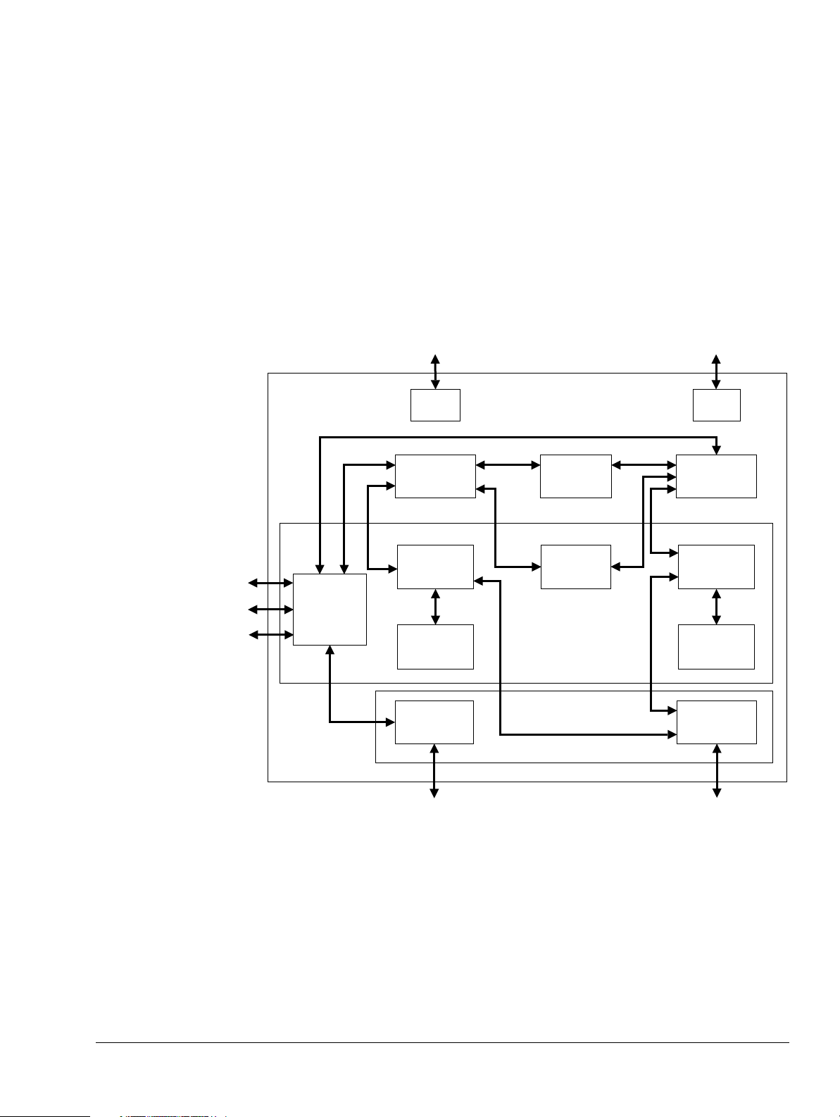
1.3 Components of the processor
This section describes the main components of the processor:
• Data Processing Unit on page 1-5
• Load/store unit on page 1-5
• Prefetch unit on page 1-5
• L1 memory system on page 1-5
• L2 AXI interfaces on page 1-7
• Debug on page 1-8
• System control coprocessor on page 1-9
• Interrupt handling on page 1-9.
Figure 1-1 shows the structure of the processor.
Introduction
ATCM
B1TCM
B0TCM
Processor
Coupled
Memory
interface
Tightly-
(TCM)
ETM
ETM
interface
Data
Prefetch Unit
Level one memory system
L1
instruction
cache control
L1
instruction
cache RAM
L2 interface
AXI
slave port
Processing
Unit
Memory
Protection
Unit
Level two interface
Debug
Debug
interface
Load/Store
Unit
L1
data cache
control
L1
data
cache RAM
L2 interface
AXI
master port
AXI slave bus
AXI master bus
Figure 1-1 Processor block diagram
The PreFetch Unit (PFU) fetches instructions from the memory system, predicts branches, and
passes instructions to the Data Processing Unit (DPU). The DPU executes all instructions and
uses the Load/Store Unit (LSU) for data memory transfers. The PFU and LSU interface to the
L1 memory system that contains L1 instruction and data caches and an interface to a L2 system.
The L1 memory can also contain optional TCM interfaces.
ARM DDI 0363E Copyright © 2009 ARM Limited. All rights reserved. 1-4
ID013010 Non-Confidential, Unrestricted Access
Page 26

1.3.1 Data Processing Unit
The DPU holds most of the program-visible state of the processor, such as general-purpose
registers, status registers and control registers. It decodes and executes instructions, operating
on data held in the registers in accordance with the ARM Architecture. Instructions are fed to
the DPU from the PFU through a buffer. The DPU performs instructions that require data to be
transferred to or from the memory system by interfacing to the LSU. See Chapter 2
Programmer’s Model for more information.
Floating Point Unit
The Floating Point Unit (FPU) is an optional part of the DPU which includes the VFP register
file and status registers. It performs floating-point operations on the data held in the VFP register
file. See Chapter 12 FPU Programmer’s Model for more information.
1.3.2 Load/store unit
The LSU manages all load and store operations, interfacing with the DPU to the TCMs, caches,
and L2 memory interfaces.
1.3.3 Prefetch unit
Introduction
The PFU obtains instructions from the instruction cache, the TCMs, or from external memory
and predicts the outcome of branches in the instruction stream. See Chapter 5 Prefetch Unit for
more information.
Branch prediction
The branch predictor is a global type that uses history registers and a 256-entry pattern history
table.
Return stack
The PFU includes a 4-entry return stack to accelerate returns from procedure calls. For each
procedure call, the return address is pushed onto a hardware stack. When a procedure return is
recognized, the address held in the return stack is popped, and the prefetch unit uses it as the
predicted return address.
1.3.4 L1 memory system
The processor L1 memory system includes the following features:
• separate instruction and data caches
• flexible TCM interfaces
• 64-bit datapaths throughout the memory system
• MPU that supports configurable memory region sizes
• export of memory attributes for L2 memory system
• parity or ECC supported on local memories.
For more information of the blocks in the L1 memory system, see:
• Instruction and data caches on page 1-6
• Memory Protection Unit on page 1-6
• TCM interfaces on page 1-6
• Error correction and detection on page 1-7.
ARM DDI 0363E Copyright © 2009 ARM Limited. All rights reserved. 1-5
ID013010 Non-Confidential, Unrestricted Access
Page 27

Introduction
Instruction and data caches
You can configure the processor to include separate instruction and data caches. The caches
have the following features:
• Support for independent configuration of the instruction and data cache sizes between
4KB and 64KB.
• Pseudo-random cache replacement policy.
• 8-word cache line length. Cache lines can be either write-back or write-through,
determined by MPU region.
• Ability to disable each cache independently.
• Streaming of sequential data from
LDM
and
LDRD
operations, and sequential instruction
fetches.
• Critical word first filling of the cache on a cache miss.
• Implementation of all the cache RAM blocks and the associated tag and valid RAM
blocks using standard ASIC RAM compilers
• Parity or ECC supported on local memories.
Memory Protection Unit
An optional MPU provides memory attributes for embedded control applications. You can
configure the MPU to have eight or twelve regions, each with a minimum resolution of 32 bytes.
MPU regions can overlap, and the highest numbered region has the highest priority.
The MPU checks for protection and memory attributes, and some of these can be passed to an
external L2 memory system.
For more information, see Chapter 7 Memory Protection Unit.
TCM interfaces
Because some applications might not respond well to caching, there are two TCM interfaces that
permit connection to configurable memory blocks of Tightly-Coupled Memory (ATCM and
BTCM). These ensure high-speed access to code or data. As an option, the BTCM can have two
memory ports for increased bandwidth.
An ATCM typically holds interrupt or exception code that must be accessed at high speed,
without any potential delay resulting from a cache miss.
A BTCM typically holds a block of data for intensive processing, such as audio or video
processing.
You can individually configure the TCM blocks at any naturally aligned address in the memory
map. Permissible TCM block sizes are:
•0KB
•4KB
•8KB
• 16KB
• 32KB
• 64KB
• 128KB
• 256KB
ARM DDI 0363E Copyright © 2009 ARM Limited. All rights reserved. 1-6
ID013010 Non-Confidential, Unrestricted Access
Page 28

Introduction
• 512KB
•1MB
•2MB
•4MB
•8MB.
The TCMs are external to the processor. This provides flexibility in optimizing the TCM
subsystem for performance, power, and RAM type. The INITRAMA and INITRAMB pins
enable booting from the ATCM or BTCM, respectively. Both the ATCM and BTCM support
wait states.
For more information, see Chapter 8 Level One Memory System.
Error correction and detection
To increase the tolerance of the system to soft memory faults, you can configure the caches for
either:
• parity generation and error correction/detection
• ECC code generation, single-bit error correction, and two-bit error detection.
Similarly, you can configure the TCM interfaces for:
• parity generation and error detection
• ECC code generation, single-bit error correction, and two-bit error detection.
1.3.5 L2 AXI interfaces
For more information, see Chapter 8 Level One Memory System.
The L2 AXI interfaces enable the L1 memory system to have access to peripherals and to
external memory using an AXI master and AXI slave port.
AXI master interface
The AXI master interface provides a high bandwidth interface to second level caches, on-chip
RAM, peripherals, and interfaces to external memory. It consists of a single AXI port with a
64-bit read channel and a 64-bit write channel for instruction and data fetches.
The AXI master can run at the same frequency as the processor, or at a lower synchronous
frequency. If asynchronous clocking is required an external asynchronous AXI slice is required.
AXI slave interface
The AXI slave interface enables AXI masters, including the AXI master port of the processor,
to access data and instruction cache RAMs and TCMs on the AXI system bus. You can use this
for DMA into and out of the TCM RAMs and for software test of the TCM and cache RAMs.
The slave interface can run at the same frequency as the processor or at a lower, synchronous
frequency. If asynchronous clocking is required an external asynchronous AXI slice is required.
Bits in the Auxiliary Control Register and Slave Port Control Register can control access to the
AXI slave. Access to the TCM RAMs can be granted to any master, to only privileged masters,
or completely disabled. Access to the cache RAMs can be separately controlled in a similar way.
ARM DDI 0363E Copyright © 2009 ARM Limited. All rights reserved. 1-7
ID013010 Non-Confidential, Unrestricted Access
Page 29

1.3.6 Debug
Introduction
The processor has a CoreSight compliant Advanced Peripheral Bus version 3 (APBv3) debug
interface. This permits system access to debug resources, for example, the setting of
watchpoints and breakpoints.
The processor provides extensive support for real-time debug and performance profiling.
The following sections give an overview of debug:
• System performance monitoring
• ETM interface
• Real-time debug facilities.
System performance monitoring
This is a group of counters that you can configure to monitor the operation of the processor and
memory system. For more information, see About the PMU on page 6-6.
ETM interface
The Embedded Trace Macrocell (ETM) interface enables you to connect an external ETM unit
to the processor for real-time code tracing of the core in an embedded system.
The ETM interface collects various processor signals and drives these signals from the
processor. The interface is unidirectional and runs at the full speed of the processor. The ETM
interface connects directly to the external ETM unit without any additional glue logic. You can
disable the ETM interface for power saving. For more information, see the CoreSight ETM-R4
Technical Reference Manual.
Real-time debug facilities
The processor contains an EmbeddedICE-RT logic unit to provide real-time debug facilities. It
has:
• up to eight breakpoints
• up to eight watchpoints
•a Debug Communications Channel (DCC).
Note
The number of breakpoints and watchpoints is configured during implementation, see
Configurable options on page 1-13.
The EmbeddedICE-RT logic monitors the internal address and data buses. You access the
EmbeddedICE-RT logic through a memory-mapped APB interface.
The processor implements the ARMv7 Debug architecture, including the extensions of the
architecture to support CoreSight.
To get full access to the processor debug capability, you can access the debug register map
through the APBv3 slave port. See Chapter 11 Debug for more information on debug.
ARM DDI 0363E Copyright © 2009 ARM Limited. All rights reserved. 1-8
ID013010 Non-Confidential, Unrestricted Access
Page 30

The EmbeddedICE-RT logic supports two modes of debug operation:
Halt mode On a debug event, such as a breakpoint or watchpoint, the debug logic stops the
Monitor debug mode
1.3.7 System control coprocessor
The system control coprocessor provides configuration and control of the memory system and
its associated functionality. Other system-level operations, such as memory barrier instructions,
are also managed through the system control coprocessor.
Introduction
processor and forces it into debug state. This enables you to examine the internal
state of the processor, and the external state of the system, independently from
other system activity. When the debugging process completes, the processor and
system state are restored, and normal program execution resumes.
On a debug event, the processor generates a debug exception instead of entering
debug state, as in halt mode. The exception entry enables a debug monitor
program to debug the processor while enabling critical interrupt service routines
to operate on the processor. The debug monitor program can communicate with
the debug host over the DCC or any other communications interface in the
system.
For more information, see System control and configuration on page 4-4.
1.3.8 Interrupt handling
Interrupt handling in the processor is compatible with previous ARM architectures, but has
several additional features to improve interrupt performance for real-time applications.
VIC port
The core has a dedicated port that enables an external interrupt controller, such as the ARM
PrimeCell Vectored Interrupt Controller (VIC), to supply a vector address along with an
Interrupt Request (IRQ) signal. This provides faster interrupt entry, but you can disable it for
compatibility with earlier interrupt controllers.
If you do not have a VIC in your design, you must ensure the nIRQ and nFIQ signals are
asserted, held LOW, and remain LOW until the exception handler clears them.
Low interrupt latency
On receipt of an interrupt, the processor abandons any pending restartable memory operations.
Restartable memory operations are the multiword transfer instructions
and
Note
POP
that can access Normal memory.
LDM, LDRD, STRD, STM, PUSH
,
To minimize the interrupt latency, ARM recommends that you do not perform:
• multiple accesses to areas of memory marked as Device or Strongly Ordered
• SWP operations to slow areas of memory.
Exception processing
The ARMv7-R architecture contains exception processing instructions to reduce interrupt
handler entry and exit time:
SRS Save return state to a specified stack frame.
ARM DDI 0363E Copyright © 2009 ARM Limited. All rights reserved. 1-9
ID013010 Non-Confidential, Unrestricted Access
Page 31

Introduction
RFE Return from exception using data from the stack.
CPS Change processor state, such as interrupt mask setting and clearing, and mode
changes.
ARM DDI 0363E Copyright © 2009 ARM Limited. All rights reserved. 1-10
ID013010 Non-Confidential, Unrestricted Access
Page 32

1.4 External interfaces of the processor
The processor has the following interfaces for external access:
• APB Debug interface
• ETM interface
• Test interface.
For more information on these interfaces and how they are integrated into the system, see the
AMBA 3 APB Protocol Specification and the CoreSight Architecture Specification.
1.4.1 APB Debug interface
AMBA APBv3 is used for debugging purposes. CoreSight is the ARM architecture for
multi-processor trace and debug. CoreSight defines what debug and trace components are
required and how they are connected.
Note
The APB debug interface can also connect to a DAP-Lite. For more information on the
DAP-Lite, see the CoreSight DAP-Lite Technical Reference Manual.
Introduction
1.4.2 ETM interface
1.4.3 Test interface
You can connect an ETM-R4 to the processor through the ETM interface. The ETM-R4
provides instruction and data trace for the processor. For more information on how the ETM-R4
connects to the processor, see the CoreSight ETM-R4 Technical Reference Manual.
All outputs are driven directly from a register unless specified otherwise. All signals are relative
to CLKIN unless specified otherwise.
The ETM interface includes these signals:
• an instruction interface
• a data interface
• an event interface
• other connections to the ETM.
See ETM interface signals on page A-19 for information about the names of signals that form
these interfaces. See Event bus interface on page 6-19 for more information about the event bus.
The test interface provides support for test during manufacture of the processor using Memory
Built-In Self Test (MBIST). For more information on the test interface, see MBIST signals on
page A-21. See the Cortex-R4 and Cortex-R4F Integration Manual for information about the
timings of these signals.
ARM DDI 0363E Copyright © 2009 ARM Limited. All rights reserved. 1-11
ID013010 Non-Confidential, Unrestricted Access
Page 33

1.5 Power management
The processor includes several microarchitectural features to reduce energy consumption:
• Accurate branch and return prediction, reducing the number of incorrect instruction fetch
and decode operations.
• The caches use sequential access information to reduce the number of accesses to the tag
RAMs and to unmatched data RAMs.
• Extensive use of gated clocks and gates to disable inputs to unused functional blocks.
Because of this, only the logic actively in use to perform a calculation consumes any
dynamic power.
The processor uses four levels of power management:
Run mode This mode is the normal mode of operation where all of the functionality
Standby mode This mode disables most of the clocks of the device, while keeping the
Introduction
of the processor is available.
device powered up. This reduces the power drawn to the static leakage
current and the minimal clock power overhead required to enable the
device to wake up from the Standby mode.
Shutdown mode This mode has the entire device powered down. All state, including cache
and TCM state, must be saved externally. The assertion of reset returns the
processor to the run state.
Dormant mode The processor can be implemented in such a way as to support Dormant
mode. Dormant mode is a power saving mode in which the processor
logic, but not the processor TCM and cache RAMs, is powered down. The
processor state, apart from the cache and TCM state, is stored to memory
before entry into Dormant mode, and restored after exit.
For more information on preparing the Cortex-R4 to support Dormant
mode, contact ARM.
For more information on the power management features, see Chapter 10 Power Control.
ARM DDI 0363E Copyright © 2009 ARM Limited. All rights reserved. 1-12
ID013010 Non-Confidential, Unrestricted Access
Page 34

1.6 Configurable options
Table 1-1 shows the features of the processor that can be configured using either
build-configuration or pin-configuration. See Product documentation, design flow, and
architecture on page 1-21 for information about configuration of the processor. Many of these
features, if included, can also be enabled and disabled during software configuration.
Introduction
Table 1-1 Configurable options
Feature Options Sub-options
Redundant core Single-core (no redundancy) - Build
Dual-core (redundant) In-phase clocks
Out-of-phase clocks
Instruction cache No i-cache - Build
i-cache included No error checking
Parity error checking
64-bit ECC error checking
4KB (4x1KB ways)
8KB (4x2KB ways)
16KB (4x4KB ways)
32KB (4x8KB ways)
64KB (4x16KB ways)
Data cache No d-cache - Build
d-cache included No error checking
Parity error checking
32-bit ECC error checking
4KB (4x1KB ways)
8KB (4x2KB ways)
16KB (4x4KB ways)
32KB (4x8KB ways)
64KB (4x16KB ways)
Build-configuration
or pin-configuration
Build
Build
Build
Build
Build
ATCM No ATCM ports - Build and pin
One ATCM port No error checking
Parity error checking
32-bit ECC error checking
64-bit ECC error checking
4KB, 8KB, 16KB, 32KB, 64KB,
128KB, 256KB, 512KB, 1MB, 2MB,
4MB, or 8MB
ARM DDI 0363E Copyright © 2009 ARM Limited. All rights reserved. 1-13
ID013010 Non-Confidential, Unrestricted Access
Build
Pin
Page 35

Introduction
Table 1-1 Configurable options (continued)
Feature Options Sub-options
Build-configuration
or pin-configuration
BTCM No BTCM ports - Build and pin
One BTCM port (B0TCM) No error checking
Build
Parity error checking
32-bit ECC error checking
64-bit ECC error checking
4KB, 8KB, 16KB, 32KB, 64KB,
Pin
128KB, 256KB, 512KB, 1MB, 2MB,
4MB, or 8MB
Two BTCM ports (B0TCM
and B1TCM)
No error checking
Parity error checking
Build
32-bit ECC error checking
64-bit ECC error checking
2x2KB, 2x4KB, 2x8KB, 2x16KB,
Pin
2x32KB, 2x64KB, 2x128KB,
2x256KB, 2x512KB, 2x1MB, 2x2MB,
or 2x4MB
Interleaved on 64-bit granularity in
Pin
memory
Adjacent in memory
Instruction
endianness
Little-endian - Build
Pin-configured Little-endian
Pin
Big-endian
Floating point
(VFP)
No FPU - Build
FPU included
a
-
MPU No MPU - Build
MPU included 8 MPU regions
Build
12 MPU regions
TCM bus parity No TCM address and control
- Build
bus parity
TCM address and control
-
bus parity generated
AXI bus parity No AXI bus parity - Build
AXI bus parity generated/
-
checked
Breakpoints 2-8 breakpoint register pairs - Build
Watchpoints 1-8 watchpoint registers - Build
ATCM at reset Disabled - Pin
Enabled
b
Base address
0x0
Pin and build
Base address configured
ARM DDI 0363E Copyright © 2009 ARM Limited. All rights reserved. 1-14
ID013010 Non-Confidential, Unrestricted Access
Page 36

Introduction
Table 1-1 Configurable options (continued)
Feature Options Sub-options
Build-configuration
or pin-configuration
BTCM at reset Disabled - Pin
Peripheral ID
b
Enabled
Any 4-bit value - Build
Base address configured
Base address
0x0
Pin and build
RevAnd field
AXI slave
No AXI-slave - Build
interface
AXI-slave included -
TCM Hard Error
Cache
Non-Maskable
FIQ Interrupt
No TCM Hard Error Cache - Build
TCM Hard Error Cache
included
c
Disabled (FIQ can be
-
-Pin
masked by software
Enabled -
Parity type
d
Odd parity - Pin
Even parity -
a. Only available with the Cortex-R4F processor.
b. Only if the relevant TCM port(s) are included.
c. Only if at least one TCM port is included and uses ECC error checking.
d. Only relevant if at least one TCM port is included and uses parity error checking, one of the caches includes parity checking,
or AXI or TCM bus parity is included.
Table 1-2 describes the various features that can be pin-configured to be either enabled or
disabled at reset. It also shows which CP15 register field provides software configuration of the
feature when the processor is out of reset. All of these fields exist in either the system control
register, or one of the auxiliary control registers.
Table 1-2 Configurable options at reset
Feature Options Register
Exception endianness Little-endian/big-endian data for exception handling EE
Exception state ARM/Thumb state for exception handling TE
Exception vector table Base address for exception vectors:
TCM error checking
ATCM parity check enable
a
BTCM parity check enable, for B0TCM and B1TCM independently
ATCM ECC check enable
a
BTCM ECC check enabled, for B0TCM and B1TCM together
0x00000000/0xFFFF0000
V
AT C M PC E N
a
B0TCMPCEN/
B1TCMPCEN
AT C M PC E N
a
B0TCMPCEN/
B1TCMPCEN
ARM DDI 0363E Copyright © 2009 ARM Limited. All rights reserved. 1-15
ID013010 Non-Confidential, Unrestricted Access
Page 37

Introduction
Table 1-2 Configurable options at reset (continued)
Feature Options Register
TCM external errors ATCM external error enable ATCMECEN
BTCM external error enable, for B0TCM and B1TCM independently B0TCMECEN/
B1TCMECEN
TCM load/store-64
ATCM load/store-64 enable
(read-modify-write) behavior
BTCM load/store-64 enable
a. Can only be enabled if the appropriate TCM is configured with the appropriate error checking scheme, and the appropriate
number of ports
b. Can only be enabled if the appropriate TCM is not configured with 32-bit ECC.
b
b
ATCMRMW
BTCMRMW
ARM DDI 0363E Copyright © 2009 ARM Limited. All rights reserved. 1-16
ID013010 Non-Confidential, Unrestricted Access
Page 38

1.7 Execution pipeline stages
The following stages make up the pipeline:
• the Fetch stages
• the Decode stages
• an Issue stage
• the three or four Execution stages.
Figure 1-2 shows the Fetch and Decode pipeline stages of the processor and the pipeline
operations that can take place at each stage.
Introduction
Fe1 Fe2 Pd De
st
1
fetch
stage
Predicted branches and returns
nd
2
stage
fetch
Instruction
formatting
branch
predicting
Instruction
decode
Figure 1-2 Processor Fetch and Decode pipeline stages
The names of the pipeline stages and their functions are:
Fe Instruction fetch where data is returned from instruction memory.
Pd Pre-decode where instructions are formatted and branch prediction occurs.
De Instruction decode.
Figure 1-3 shows the Issue and Execution pipeline stages for the Cortex-R4 processor.
Iss Ex1 Ex2 Wr
Register
read,
address
generation,
and
instruction
issue
DC1
EX1
DC2
EX1
Wr
Ret
Load/store
pipeline
Data
processing
pipeline
Mispredicted direct branches
Exception flush and mispredicted
indirect branches
Figure 1-3 Cortex-R4 Issue and Execution pipeline stages
Figure 1-4 on page 1-18 shows the Issue and Execution pipeline stages for the Cortex-R4F
processor.
ARM DDI 0363E Copyright © 2009 ARM Limited. All rights reserved. 1-17
ID013010 Non-Confidential, Unrestricted Access
Page 39

Introduction
Iss Ex1 Ex2 Wr
Register
read,
address
generation,
and
instruction
issue
DC1
EX1
F0
Mispredicted direct branches
Exception flush and mispredicted
indirect branches
DC2
EX1
F1 F2
Wr
Figure 1-4 Cortex-R4F Issue and Execution pipeline stages
The names of the common pipeline stages and their functions are:
Iss Register read and instruction issue to execute stages.
Ex Execute stages.
Wr Write-back of data from the execution pipelines.
Ret Instruction retire.
Ret
Fwr
Load/store
pipeline
Data
processing
pipeline
Floating point
pipeline
The names of the load/store pipeline stages and their functions are:
DC1 First stage of data memory access.
DC2 Second stage of data memory access.
The names of the floating point pipeline stages and their functions are:
F0 Floating point register read.
F1 First stage of floating point execution.
F2 Second stage of floating point execution.
Fwr Floating point writeback.
The pipeline structure provides a pipelined 2-cycle memory access and single-cycle load-use
penalty. This enables integration with slow RAM blocks and maintains good CPI at reasonable
frequencies.
ARM DDI 0363E Copyright © 2009 ARM Limited. All rights reserved. 1-18
ID013010 Non-Confidential, Unrestricted Access
Page 40

1.8 Redundant core comparison
The processor can be implemented with a second, redundant copy of most of the logic. This
second core shares the input pins and the cache RAMs of the master core, so only one set of
cache RAMs is required. The master core drives the output pins and the cache RAMs.
Comparison logic can be included during implementation which compares the outputs of the
redundant core with those of the master core. If a fault occurs in the logic of either core, because
of radiation or circuit failure, this is detected by the comparison logic. Used in conjunction with
the RAM error detection schemes, this can help protect the system from faults. The inputs
DCCMINP[7:0] and DCCMINP2[7:0] and the outputs DCCMOUT[7:0] and
DCCMOUT2[7:0] enable the comparison logic inside the processor to communicate with the
rest of the system.
ARM provides example comparison logic, but you can change this during implementation. If
you are implementing a processor with dual-redundant cores, contact ARM for more
information. If you are integrating a Cortex-R4 macrocell with dual-redundant cores, contact the
implementer for more details.
Introduction
ARM DDI 0363E Copyright © 2009 ARM Limited. All rights reserved. 1-19
ID013010 Non-Confidential, Unrestricted Access
Page 41

1.9 Test features
Introduction
The processor is delivered as fully-synthesizable RTL and is a fully-static design. Scan-chains
and test wrappers for production test can be inserted into the design by the synthesis tools during
implementation. See the relevant reference methodology documentation for more information.
Production test of the processor cache and TCM RAMs can be done through the dedicated,
pipelined MBIST interface. This interface shares some of the multiplexing present in the
processor design, which improves the potential frequency compared to adding multiplexors to
the RAM modules. See the Cortex-R4 and Cortex-R4F Integration Manual for more
information about this interface, and how to control it.
In addition, you can use the AXI slave interface to read and write the cache and TCM RAMs.
You can use this feature to test the cache RAMs in a running system. This might be required in
a safety-critical system. The TCM RAMs can be read and written directly by the program
running on the processor. You can also use the AXI slave interface for swapping a test program
in to the TCMs for the processor to execute. See Accessing RAMs using the AXI slave interface
on page 9-24 for more information about how to access the RAMs using the AXI slave interface.
ARM DDI 0363E Copyright © 2009 ARM Limited. All rights reserved. 1-20
ID013010 Non-Confidential, Unrestricted Access
Page 42

1.10 Product documentation, design flow, and architecture
This section describes the content of the product documents, how they relate to the design flow,
and the relevant architectural standards and protocols.
Note
See Further reading on page xx for more information about the documentation described in this
section.
1.10.1 Documentation
The following books describe the processor:
Technical Reference Manual
The Technical Reference Manual (TRM) describes the processor functionality
and the effects of functional options on the behavior of the processor. It is required
at all stages of the design flow. Some behavior described in the TRM might not
be relevant, because of the way the processor has been implemented and
integrated. If you are programming the processor, contact the implementer to
determine the build configuration of the implementation, and the integrator to
determine the pin configuration of the SoC that you are using.
Introduction
1.10.2 Design flow
Configuration and Sign-Off Guide
The Configuration and Sign-Off Guide (CSG) describes:
• the available build configuration options and related issues in selecting
them
• how to configure the Register Transfer Level (RTL) with the build
configuration options
• the processes to sign off the configured RTL and final macrocell.
The ARM product deliverables include reference scripts and information about
using them to implement your design. Reference methodology documentation
from your EDA tools vendor complements the CSG. The CSG is a confidential
book that is only available to licensees.
Integration Manual
The Integration Manual (IM) describes how to integrate the processor into a SoC
including describing the pins that the integrator must tie off to configure the
macrocell for the required integration. Some of the integration is affected by the
configuration options that were used to implement the processor. Contact the
implementer of the macrocell that you are using to determine the implemented
build configuration options. The IM is a confidential book that is only available
to licensees.
The processor is delivered as synthesizable RTL. Before it can be used in a product, it must go
through the following process:
1. Implementation. The implementer configures and synthesizes the RTL to produce a hard
macrocell. This includes integrating the cache RAMs into the design.
2. Integration. The integrator integrates the hard macrocell into a SoC, connecting it to a
memory system and to appropriate peripherals for the intended function. This memory
system includes the Tightly Coupled Memories (TCMs).
ARM DDI 0363E Copyright © 2009 ARM Limited. All rights reserved. 1-21
ID013010 Non-Confidential, Unrestricted Access
Page 43

Introduction
3. Programming. The system programmer develops the software required to configure and
initialize the processor, and possibly tests the required application software on the
processor.
Each of these stages can be performed by a different company. Configuration options are
available at each stage. These options affect the behavior and available features at the next stage:
Build configuration
The implementer chooses the options that affect how the RTL source files are
pre-processed. They usually include or exclude logic that can affect the area or
maximum frequency of the resulting macrocell.
For example, the BTCM interface can be configured to have zero, one (B0TCM)
or two (B0TCM and B1TCM) ports. If one port is chosen, the logic for the second
port is excluded from the macrocell, although the pins remain, and the second port
(B1TCM) cannot be used on that macrocell.
Configuration inputs
The integrator configures some features of the processor by tying inputs to
specific values. These configurations affect the start-up behavior before any
software configuration is made. They can also limit the options available to the
software.
For example, if the build configuration for the macrocell includes both BTCM
ports, the integrator can choose how many ports to actually use, and therefore
how many RAMs must be integrated with the macrocell. If the integrator only
wishes to use one BTCM port, they can connect RAM to the B0TCM port only,
and tie the ENTCM1IF input to zero to indicate that the B1TCM is not available.
Software configuration
Note
This manual refers to implementation-defined features that are applicable to build configuration
options. References to a feature which is included mean that the appropriate build and pin
configuration options have been selected, while references to an enabled feature mean one that
has also been configured by software.
1.10.3 Architectural information
The Cortex-R4 processor conforms to, or implements, the following specifications:
ARM Architecture
The programmer configures the processor by programming particular values into
software-visible registers. This affects the behavior of the processor.
For example, the enable bit in the BTCM Region Register controls whether or not
memory accesses are performed to the BTCM interface. However, the BTCM
cannot, and must not, be enabled if the build configuration does not include any
BTCM ports, or if the pin configuration indicates that no RAMs have been
integrated onto the BTCM ports.
This describes:
• The behavior and encoding of the instructions that the processor can
execute.
• The modes and states that the processor can be in.
• The various data and control registers that the processor must contain.
ARM DDI 0363E Copyright © 2009 ARM Limited. All rights reserved. 1-22
ID013010 Non-Confidential, Unrestricted Access
Page 44

Introduction
• The properties of memory accesses.
• The debug architecture you can use to debug the processor. The TRM gives
more information about the implemented debug features.
The Cortex-R4 processor implements the ARMv7-R architecture profile.
Advanced Microcontroller Bus Architecture protocol
Advanced Microcontroller Bus Architecture (AMBA) is an open standard,
on-chip bus specification that defines the interconnection and management of
functional blocks that make up a System-on-Chip (SoC). It facilitates
development of embedded processors with multiple peripherals.
IEEE 754 This is the IEEE Standard for Binary Floating Point Arithmetic.
An architecture specification typically defines a number of versions, and includes features that
are either optional or partially specified. The TRM describes which architectures are used,
including which version is implemented, and the architectural choices made for the
implementation. The TRM does not provide detailed information about the architecture, but
some architectural information is included to give an overview of the implementation or, in the
case of control registers, to make the manual easier to use. See the appropriate specification for
more information about the implemented architectural features.
ARM DDI 0363E Copyright © 2009 ARM Limited. All rights reserved. 1-23
ID013010 Non-Confidential, Unrestricted Access
Page 45

1.11 Product revision information
This manual is for major revision 1 of the processor. At the time of release, this includes the
r1p0, r1p1, r1p2, and r1p3 releases, although the vast majority of the information in this
document will also be applicable to any future r1px releases. The following broadly describes
the changes made in each subsequent revision of the processor:
Revision 1 Introduction of the ECC functional options and addition of the FPU options, to
implement the Cortex-R4F processor.
Note
The r1p0 release was not generally available.
1.11.1 Processor identification
The Cortex-R4 processor contains a number of IDentification (ID) registers that enable software
or a debugger to identify the processor as Cortex-R4, and the variant (major revision) and
revision (minor revision) of the design. These registers are:
Main ID Register (MIDR)
This register is accessible by software and identifies the part, the variant, and the
revision. See c0, Main ID Register on page 4-14. A copy of this register can also
be read by a debugger through the debug APB interface. See Processor ID
Registers on page 11-32.
Introduction
Debug ID Register (DIDR)
This register can be read by a debugger through the debug APB interface, and by
software. It identifies the variant and revision. See CP14 c0, Debug ID Register
on page 11-10.
Peripheral ID Registers
These registers can be accessed through the debug APB interface only, and
identify the revision number of the processor. See Debug Identification Registers
on page 11-35.
Floating Point System ID Register (FPSID)
When the build-configuration includes the floating point unit, this register
identifies the revision number of the floating-point unit. See Floating-Point
System ID Register, FPSID on page 12-5.
Note
Floating point functionality is provided only with the Cortex-R4F processor.
The revision number of the processor, in the Peripheral ID and FPSID registers, is a single field
that incorporates information about both major and minor revisions.
ARM DDI 0363E Copyright © 2009 ARM Limited. All rights reserved. 1-24
ID013010 Non-Confidential, Unrestricted Access
Page 46

Introduction
Table 1-3 shows the mappings between these various numbers, for all releases.
Table 1-3 ID values for different product versions
ID value r0p0 r0p1 r0p2 r0p3 r1p0 r1p1 r1p2 r1p3
Variant field, Main ID Register
Revision field, Main ID Register
Variant field, Debug ID Register
Revision field, Debug ID Register
Revision number, Peripheral ID Registers
Revision number, FPSID Register - - - -
1.11.2 Architectural information
The ARM Architecture includes a number of registers that identify the version of the
architecture and some of the architectural features that a processor implements. Chapter 4
System Control Coprocessor describes the values that the processor implements for the fields in
these registers. For details of the possible values and their meanings for these fields, see the
ARM Architecture Reference Manual.
0x0 0x0 0x0 0x0 0x1
0x0 0x1 0x2 0x3 0x0
0x0 0x0 0x0 0x0 0x1
0x0 0x1 0x2 0x3 0x0
0x0 0x1 0x2 0x5 0x3
0x3
0x1 0x1
0x1 0x2
0x1 0x1
0x1 0x2
0x4 0x6
0x4 0x6
0x1
0x3
0x1
0x3
0x7
0x7
ARM DDI 0363E Copyright © 2009 ARM Limited. All rights reserved. 1-25
ID013010 Non-Confidential, Unrestricted Access
Page 47

Chapter 2
Programmer’s Model
This chapter describes the processor registers and provides an overview for programming the
microprocessor. It contains the following sections:
• About the programmer’s model on page 2-2
• Instruction set states on page 2-3
• Operating modes on page 2-4
• Data types on page 2-5
• Memory formats on page 2-6
• Registers on page 2-7
• Program status registers on page 2-10
• Exceptions on page 2-16
• Acceleration of execution environments on page 2-27
• Unaligned and mixed-endian data access support on page 2-28
• Big-endian instruction support on page 2-29.
ARM DDI 0363E Copyright © 2009 ARM Limited. All rights reserved. 2-1
ID013010 Non-Confidential, Unrestricted Access
Page 48

2.1 About the programmer’s model
The processor implements the ARMv7-R architecture that provides:
• the 32-bit ARM instruction set
• the extended Thumb instruction set introduced in ARMv6T2, that uses Thumb-2
technology to provide a wide range of 32-bit instructions.
For more information on the ARM and Thumb instruction sets, see the ARM Architecture
Reference Manual. This chapter describes some of the main features of the architecture but, for
a complete description, see the ARM Architecture Reference Manual.
This chapter also makes reference to older versions of the ARM architecture that the processor
does not implement. These references are included to contrast the behavior of the Cortex-R4
processor with other processors you might have used that implement an older version of the
architecture.
Programmer’s Model
ARM DDI 0363E Copyright © 2009 ARM Limited. All rights reserved. 2-2
ID013010 Non-Confidential, Unrestricted Access
Page 49

2.2 Instruction set states
The processor has two instruction set states:
ARM state The processor executes 32-bit, word-aligned ARM instructions in this
Thumb state The processor executes 32-bit and 16-bit halfword-aligned Thumb
Note
Transition between ARM state and Thumb state does not affect the processor mode or the
register contents.
2.2.1 Switching state
The instruction set state of the processor can be switched between ARM state and Thumb state:
Programmer’s Model
state.
instructions in this state.
• Using the
BX
and
that does not set flags, with the PC as the destination register. Switching state is described
in the ARM Architecture Reference Manual.
Note
When the
BXJ
instruction is used the processor invokes the BX instruction.
• Automatically on an exception. You can write an exception handler routine in ARM or
Thumb code. For more information, see Exceptions on page 2-16.
2.2.2 Interworking ARM and Thumb state
The processor enables you to mix ARM and Thumb code. For more information about
interworking ARM and Thumb, see the RealView Compilation Tools Developer Guide.
BLX
instructions, by a load to the PC, or with a data-processing instruction
ARM DDI 0363E Copyright © 2009 ARM Limited. All rights reserved. 2-3
ID013010 Non-Confidential, Unrestricted Access
Page 50

2.3 Operating modes
In each state there are seven modes of operation:
• User (USR) mode is the usual mode for the execution of ARM or Thumb programs. It is
• Fast interrupt (FIQ) mode is entered on taking a fast interrupt.
• Interrupt (IRQ) mode is entered on taking a normal interrupt.
• Supervisor (SVC) mode is a protected mode for the operating system and is entered on
• Abort (ABT) mode is entered after a data or instruction abort.
• System (SYS) mode is a privileged user mode for the operating system.
• Undefined (UND) mode is entered when an Undefined instruction exception occurs.
Modes other than User mode are collectively known as Privileged modes. Privileged modes are
used to service interrupts or exceptions, or access protected resources.
Programmer’s Model
used for executing most application programs.
taking a Supervisor Call (SVC), formerly SWI.
ARM DDI 0363E Copyright © 2009 ARM Limited. All rights reserved. 2-4
ID013010 Non-Confidential, Unrestricted Access
Page 51

2.4 Data types
Programmer’s Model
The processor supports these data types:
• doubleword, 64-bit
• word, 32-bit
• halfword, 16-bit
• byte, 8-bit.
Note
• When any of these types are described as unsigned, the N-bit data value represents a
N
non-negative integer in the range 0 to +2
-1, using normal binary format.
• When any of these types are described as signed, the N-bit data value represents an integer
in the range -2
N-1
to +2
N-1
-1, using two’s complement format.
For best performance you must align these data types in memory as follows:
• doubleword quantities aligned to 8-byte boundaries, doubleword aligned
• word quantities aligned to 4-byte boundaries, word aligned
• halfword quantities aligned to 2-byte boundaries halfword aligned
• byte quantities can be placed on any byte boundary.
The processor supports mixed-endian and unaligned access. For more information, see
Unaligned and mixed-endian data access support on page 2-28.
Note
You cannot use
LDRD, LDM, STRD
, or
STM
instructions to access 32-bit quantities if they are not
32-bit aligned.
ARM DDI 0363E Copyright © 2009 ARM Limited. All rights reserved. 2-5
ID013010 Non-Confidential, Unrestricted Access
Page 52

2.5 Memory formats
The processor views memory as a linear collection of bytes numbered in ascending order from
zero. For example, bytes 0-3 hold the first stored word, and bytes 4-7 hold the second stored
word.
The processor can treat words of data in memory as being stored in either:
• Byte-invariant big-endian format
• Little-endian format.
Additionally, the processor supports mixed-endian and unaligned data accesses. For more
information, see the ARM Architecture Reference Manual.
2.5.1 Byte-invariant big-endian format
In byte-invariant big-endian (BE-8) format, the processor stores the most significant byte of a
word at the lowest-numbered byte, and the least significant byte at the highest-numbered byte.
Figure 2-1 shows byte-invariant big-endian (BE-8) format.
Programmer’s Model
2.5.2 Little-endian format
In little-endian format, the lowest-numbered byte in a word is the least significant byte of the
word and the highest-numbered byte is the most significant. Figure 2-2 shows little-endian
format.
Address
A[31:0]
Address
A[31:0]
Memory Register
07
31 24 23 16 15 8 7 0
msbyte
B0
+1
B1
+2
B2
B3
lsbyte
+3
Figure 2-1 Byte-invariant big-endian (BE-8) format
Memory Register
07
31 24 23 16 15 8 7 0
lsbyte
b0
B3B2B0 B1
b0b1b3 b2
+1
b1
+2
b2
b3
msbyte
+3
Figure 2-2 Little-endian format
ARM DDI 0363E Copyright © 2009 ARM Limited. All rights reserved. 2-6
ID013010 Non-Confidential, Unrestricted Access
Page 53

2.6 Registers
2.6.1 The register set
Programmer’s Model
The processor has a total of 37 program registers:
• 31 general-purpose 32-bit registers
• six 32-bit status registers.
These registers are not all accessible at the same time. The processor state and operating mode
determine the registers that are available to the programmer.
In the processor the same register set is used in both the ARM and Thumb states. Sixteen general
registers and one or two status registers are accessible at any time. In Privileged modes,
alternative mode-specific banked registers become available. Figure 2-3 on page 2-9 shows the
registers that are available in each mode.
The register set contains 16 directly-accessible registers, R0-R15. Another register, the Current
Program Status Register (CPSR), contains condition code flags, status bits, and current mode
bits. Registers R0-R12 are general-purpose registers that hold either data or address values.
Registers R13, R14, R15, and the CPSR have these special functions:
Stack pointer Software normally uses register R13 as a Stack Pointer (SP). The
RFE
instructions use Register R13.
Link Register Register R14 is used as the subroutine Link Register (LR).
Register R14 receives the return address when a Branch with Link (
BLX
) instruction is executed.
You can use R14 as a general-purpose register at all other times. The
corresponding banked registers R14_svc, R14_irq, R14_fiq, R14_abt, and
R14_und similarly hold the return values when interrupts and exceptions
are taken, or when
BL
or
BLX
instructions are executed within interrupt or
exception routines.
Program Counter Register R15 holds the PC:
• in ARM state this is word-aligned
• in Thumb state this is either word or halfword-aligned.
Note
There are special cases for reading R15:
• reading the address of the current instruction plus, either:
— 4 in Thumb state
— 8 in ARM state.
• reading
0x00000000
(zero).
There are special cases for writing R15:
• causing a branch to the address that was written to R15
• ignoring the value that was written to R15
• writing bits [31:28] of the value that was written to R15 to the
condition flags in the CPSR, and ignoring bits [27:20] (used for the
MRC
instruction only).
You must not assume any of these special cases unless it is explicitly stated
in the instruction description. Instead, you must treat instructions with
register fields equal to R15 as Unpredictable.
SRS
and
BL
or
ARM DDI 0363E Copyright © 2009 ARM Limited. All rights reserved. 2-7
ID013010 Non-Confidential, Unrestricted Access
Page 54

Programmer’s Model
For more information, see the ARM Architecture Reference Manual.
In Privileged modes, another register, the Saved Program Status Register (SPSR), is accessible.
This contains the condition code flags, status bits, and current mode bits saved as a result of the
exception that caused entry to the current mode.
Banked registers have a mode identifier that indicates which mode they relate to. Table 2-1lists
these identifiers.
Table 2 - 1 R e g i s t er mode identifiers
Mode Mode identifier
User
usr
a
Fast interrupt fiq
Interrupt irq
Supervisor svc
Abort abt
System
usr
a
Undefined und
a. The
usr
identifier is usually
omitted from register
names. It is only used in
descriptions where the User
or System mode register is
specifically accessed from
another operating mode.
FIQ mode has seven banked registers mapped to R8–R14 (R8_fiq–R14_fiq). As a result many
FIQ handlers do not have to save any registers.
The Supervisor, Abort, IRQ, and Undefined modes each have alternative mode-specific
registers mapped to R13 and R14, permitting a private stack pointer and link register for each
mode.
Figure 2-3 on page 2-9 shows the register set, and those registers that are banked.
ARM DDI 0363E Copyright © 2009 ARM Limited. All rights reserved. 2-8
ID013010 Non-Confidential, Unrestricted Access
Page 55

General registers and program counter
Programmer’s Model
System and User
R0
R1
R2
R3
R4
R5
R6
R7
R8
R9
R10
R11
R12
R13
R14
R15
FIQ
R0
R1
R2
R3
R4
R5
R6
R7
R8_fiq
R9_fiq
R10_fiq
R11_fiq
R12_fiq
R13_fiq
R14_fiq
R15 (PC)
Supervisor Abort IRQ Undefined
R0
R1
R2
R3
R4
R5
R6
R7
R8
R9
R10
R11
R12
R13_svc
R14_svc
R15 (PC) R15 (PC) R15 (PC) R15 (PC)
R0
R1
R2
R3
R4
R5
R6
R7
R8
R9
R10
R11
R12
R13_abt
R14_abt
R0
R1
R2
R3
R4
R5
R6
R7
R8
R9
R10
R11
R12
R13_irq
R14_irq
Program status registers
CPSR CPSR CPSR CPSR CPSR CPSR
SPSR_fiq SPSR_svc SPSR_abt SPSR_irq SPSR_und
R0
R1
R2
R3
R4
R5
R6
R7
R8
R9
R10
R11
R12
R13_und
R14_und
= banked register
Figure 2-3 Register organization
Note
For 16-bit Thumb instructions, the high registers, R8–R15, are not part of the standard register
set. You can use special variants of the
the range R0–R7, to a high register, and from a high register to a low register. The
enables you to compare high register values with low register values. The
MOV
instruction to transfer a value from a low register, in
CMP
ADD
instruction
enables you to add high register values to low register values. For more information, see the
ARM Architecture Reference Manual.
instruction
ARM DDI 0363E Copyright © 2009 ARM Limited. All rights reserved. 2-9
ID013010 Non-Confidential, Unrestricted Access
Page 56

2.7 Program status registers
The processor contains one CPSR and five SPSRs for exception handlers to use. The program
status registers:
• hold information about the most recently performed ALU operation
• control the enabling and disabling of interrupts
• set the processor operating mode.
Figure 2-4 shows the bit arrangement in the status registers.
31 30 29 28 27 26 25 24 23 20 19 16 15 10 9 8 7 6 5 4 0
Programmer’s Model
ZCVQ
The following sections explain the meanings of these bits:
• The N, Z, C, and V bits
• The Q bit on page 2-11
• The IT bits on page 2-11
• The J bit on page 2-12
• The DNM bits on page 2-12
• The GE bits on page 2-12
• The E bit on page 2-13
• The A bit on page 2-13
• The I and F bits on page 2-13
• The T bit on page 2-13
• The M bits on page 2-14
DNM
Greater than
or equal to
Java state bit
IT[1:0]
Sticky overflow
Overflow
Carry/Borrow/Extend
Zero
Negative/Less than
M[4:0]TFIAEIT[7:2]GE[3:0]NJ
Mode bits
Thumb state bit
FIQ disable
IRQ disable
Imprecise abort
disable bit
Data endianness bit
Figure 2-4 Program status register
2.7.1 The N, Z, C, and V bits
The N, Z, C, and V bits are the condition code flags. You can optionally set them with arithmetic
and logical operations, and also with
MSR
instructions and
MRC
instructions to R15. The processor
tests these flags in accordance with an instruction's condition code to determine whether to
execute that instruction.
In ARM state, most instructions can execute conditionally on the state of the N, Z, C, and V bits.
The exceptions are:
•
BKPT
•
CPS
•
LDC2
•
MCR2
•
MCRR2
•
MRC2
ARM DDI 0363E Copyright © 2009 ARM Limited. All rights reserved. 2-10
ID013010 Non-Confidential, Unrestricted Access
Page 57

2.7.2 The Q bit
Programmer’s Model
•
MRRC2
•
PLD
•
RFE
•
SETEND
•
SRS
•
STC2
.
In Thumb state, the processor can only execute the Branch instruction conditionally. Other
instructions can be made conditional by placing them in the If-Then (IT) block. For more
information about conditional execution in Thumb state, see the ARM Architecture Reference
Manual.
Certain multiply and fractional arithmetic instructions can set the Sticky Overflow, Q, flag:
•
QADD
•
QDADD
•
QSUB
•
QDSUB
•
SMLAD
•
SMLAxy
•
SMLAWy
•
SMLSD
•
SMUAD
•
SSAT
•
SSAT16
•
USAT
•
USAT16
.
2.7.3 The IT bits
The Q flag is sticky in that, when an instruction sets it, this bit remains set until an
MSR
instruction
writing to the CPSR explicitly clears it. Instructions cannot execute conditionally on the status
of the Q flag.
To determine the status of the Q flag you must read the PSR into a register and extract the Q flag
from this. For information of how the Q flag is set and cleared, see individual instruction
definitions in the ARM Architecture Reference Manual.
IT[7:5] encodes the base condition code for the current IT block, if any. It contains b000 when
no IT block is active.
IT[4:0] encodes the number of instructions that are to be conditionally executed, and whether
the condition for each is the base condition code or the inverse of the base condition code. It
contains b00000 when no IT block is active.
When an IT instruction is executed, these bits are set according to the condition in the
instruction, and the Then and Else (T and E) parameters in the instruction. During execution of
an IT block, IT[4:0] is shifted to:
• reduce the number of instructions to be conditionally executed by one
• move the next bit into position to form the least significant bit of the condition code.
ARM DDI 0363E Copyright © 2009 ARM Limited. All rights reserved. 2-11
ID013010 Non-Confidential, Unrestricted Access
Page 58

2.7.4 The J bit
2.7.5 The DNM bits
Programmer’s Model
For more information on the operation of the IT execution state bits, see the ARM Architecture
Reference Manual.
The J bit in the CPSR returns 0 when read.
Note
You cannot use an
MSR
to change the J bit in the CPSR.
Software must not modify the Do Not Modify (DNM) bits. These bits are:
• Readable, to preserve the state of the processor, for example, during process context
switches.
• Writable, to enable the processor to restore its state. To maintain compatibility with future
ARM processors, and as good practice, use a read-modify-write strategy when you
change the CPSR.
2.7.6 The GE bits
Instruction
Signed
SADD16
SSUB16
SADDSUBX
SSUBADDX
SADD8
SSUB8
Unsigned
UADD16
Some of the SIMD instructions set GE[3:0] as greater-than-or-equal bits for individual
halfwords or bytes of the result, as Table 2-2 shows.
Table 2-2 GE[3:0] settings
GE[3] GE[2] GE[1] GE[0]
A op B greater than
or equal to C
[31:16] + [31:16] ≥ 0 [31:16] + [31:16] ≥ 0 [15:0] + [15:0] ≥ 0 [15:0] + [15:0] ≥ 0
[31:16] - [31:16] ≥ 0 [31:16] - [31:16] ≥ 0 [15:0] - [15:0] ≥ 0 [15:0] - [15:0] ≥ 0
[31:16] + [15:0] ≥ 0 [31:16] + [15:0] ≥ 0 [15:0] - [31:16] ≥ 0 [15:0] - [31:16] ≥ 0
[31:16] - [15:0] ≥ 0 [31:16] - [15:0] ≥ 0 [15:0] + [31:16] ≥ 0 [15:0] + [31:16] ≥ 0
[31:24] + [31:24] ≥ 0 [23:16] + [23:16] ≥ 0 [15:8] + [15:8] ≥ 0 [7:0] + [7:0] ≥ 0
[31:24] - [31:24] ≥ 0 [23:16] - [23:16] ≥ 0 [15:8] - [15:8] ≥ 0 [7:0] - [7:0] ≥ 0
[31:16] + [31:16] ≥ 216[31:16] + [31:16] ≥ 2
A op B greater than
or equal to C
16
A op B greater
than or equal to C
[15:0] + [15:0] ≥ 2
16
A op B greater
than or equal to C
[15:0] + [15:0] ≥ 2
16
USUB16
UADDSUBX
USUBADDX
UADD8
USUB8
ARM DDI 0363E Copyright © 2009 ARM Limited. All rights reserved. 2-12
ID013010 Non-Confidential, Unrestricted Access
[31:16] - [31:16] ≥ 0 [31:16] - [31:16] ≥ 0 [15:0] - [15:0] ≥ 0 [15:0] - [15:0] ≥ 0
[31:16] + [15:0] ≥ 2
16
[31:16] + [15:0] ≥ 2
[31:16] - [15:0] ≥ 0 [31:16] - [15:0] ≥ 0
[31:24] + [31:24] ≥ 28[23:16] + [23:16] ≥ 2
16
[15:0] - [31:16] ≥ 0 [15:0] - [31:16] ≥ 0
[15:0] + [31:16] ≥ 2
8
[15:8] + [15:8] ≥ 2
16
[15:0] + [31:16] ≥2
8
[7:0] + [7:0] ≥ 2
[31:24] - [31:24] ≥ 0 [23:16] - [23:16] ≥ 0 [15:8] - [15:8] ≥ 0 [7:0] - [7:0] ≥ 0
16
8
Page 59

2.7.7 The E bit
Programmer’s Model
Note
GE bit is 1 if A op B ≥ C, otherwise 0.
The
SEL
instruction uses GE[3:0] to select which source register supplies each byte of its result.
Note
• For unsigned operations, the usual ARM rules determine the GE bits for carries out of
unsigned additions and subtractions, and so are carry-out bits.
• For signed operations, the rules for setting the GE bits are chosen so that they have the
same sort of greater than or equal functionality as for unsigned operations.
ARM and Thumb instructions are provided to set and clear the E bit. The E bit controls
load/store endianness. See the ARM Architecture Reference Manual for information on where
the E bit is used.
Architecture versions prior to ARMv6 specify this bit as SBZ. This ensures no endianness
reversal on loads or stores.
2.7.8 The A bit
2.7.9 The I and F bits
2.7.10 The T bit
The A bit is set automatically. It disables imprecise Data Aborts. For more information on how
to use the A bit, see Imprecise abort masking on page 2-23.
The I and F bits are the interrupt disable bits:
• when the I bit is set, IRQ interrupts are disabled
• when the F bit is set, FIQ interrupts are disabled.
Software can use
MSR, CPS, MOVS pc, SUBS pc, LDM ..,{..pc}^
, or
RFE
instructions to change the
values of the I and F bits.
When NMFIs are enabled, updates to the F bit are restricted. For more information see
Non-maskable fast interrupts on page 2-19.
The T bit reflects the instruction set state:
• when the T bit is set, the processor executes in Thumb state
• when the T bit is clear, the processor executes in ARM state.
Note
Never use an
ignores any attempt to modify the T bit using an
MSR
instruction to force a change to the state of the T bit in the CPSR. The processor
MSR
instruction.
ARM DDI 0363E Copyright © 2009 ARM Limited. All rights reserved. 2-13
ID013010 Non-Confidential, Unrestricted Access
Page 60

2.7.11 The M bits
M[4:0] Mode
b10000 User R0–R7, R8-R12, SP, LR, PC, CPSR R0–R14, PC, CPSR
Programmer’s Model
M[4:0] are the mode bits. These bits determine the processor operating mode as Table 2-3
shows.
Table 2-3 PSR mode bit values
Visible state registers
Thumb ARM
b10001 FIQ R0–R7, R8_fiq-R12_fiq, SP_fiq, LR_fiq PC,
CPSR, SPSR_fiq
b10010 IRQ R0–R7, R8-R12, SP_irq, LR_irq, PC, CPSR,
SPSR_irq
b10011 Supervisor R0–R7, R8-R12, SP_svc, LR_svc, PC, CPSR,
SPSR_svc
b10111 Abort R0–R7, R8-R12, SP_abt, LR_abt, PC, CPSR,
SPSR_abt
b11011 Undefined R0–R7, R8-R12, SP_und, LR_und, PC, CPSR,
SPSR_und
b11111 System R0–R7, R8-R12, SP, LR, PC, CPSR R0–R14, PC, CPSR
Note
• In Privileged mode an illegal value programmed into M[4:0] causes the processor to enter
System mode.
• In User mode M[4:0] can be read. Writes to M[4:0] are ignored.
2.7.12 Modification of PSR bits by MSR instructions
In architecture versions earlier than ARMv6,
[31:24], of the CPSR in any mode, but the other three bytes are only modifiable in Privileged
modes.
R0–R7, R8_fiq–R14_fiq, PC, CPSR,
SPSR_fiq
R0–R12, R13_irq, R14_irq, PC, CPSR,
SPSR_irq
R0–R12, R13_svc, R14_svc, PC, CPSR,
SPSR_svc
R0–R12, R13_abt, R14_abt, PC, CPSR,
SPSR_abt
R0–R12, R13_und, R14_und, PC, CPSR,
SPSR_und
MSR
instructions can modify the flags byte, bits
In the ARMv7-R architecture each CPSR bit falls into one of these categories:
• Bits that are freely modifiable from any mode, either directly by
MSR
instructions or by
other instructions whose side-effects include writing the specific bit or writing the entire
CPSR.
Bits in Figure 2-4 on page 2-10 that are in this category are N, Z, C, V, Q, GE[3:0], and E.
• Bits that an
of another instruction. If an
MSR
instruction must never modify, and so must only be written as a side-effect
MSR
instruction tries to modify these bits, the results are
architecturally Unpredictable. In the processor these bits are not affected.
The bits in Figure 2-4 on page 2-10 that are in this category are the execution state bits
[26:24], [15:10], and [5].
• Bits that can only be modified from Privileged modes, and that instructions completely
protect from modification while the processor is in User mode. Entering a processor
exception is the only way to modify these bits while the processor is in User mode, as
described in Exceptions on page 2-16.
ARM DDI 0363E Copyright © 2009 ARM Limited. All rights reserved. 2-14
ID013010 Non-Confidential, Unrestricted Access
Page 61

Programmer’s Model
Bits in Figure 2-4 on page 2-10 that are in this category are A, I, F, and M[4:0].
ARM DDI 0363E Copyright © 2009 ARM Limited. All rights reserved. 2-15
ID013010 Non-Confidential, Unrestricted Access
Page 62

2.8 Exceptions
Programmer’s Model
Exceptions are taken whenever the normal flow of a program must temporarily halt, for
example, to service an interrupt from a peripheral. Before attempting to handle an exception, the
processor preserves the critical parts of the current processor state so that the original program
can resume when the handler routine has finished.
This section provides information of the processor exception handling:
• Exception entry and exit summary
• Reset on page 2-18
• Interrupts on page 2-18
• Aborts on page 2-22
• Supervisor call instruction on page 2-24
• Undefined instruction on page 2-25
• Breakpoint instruction on page 2-25
• Exception vectors on page 2-26.
Note
When the processor is in debug halt state, and an exception occurs, it is handled differently to
normal. See Exceptions in debug state on page 11-47 for more details
2.8.1 Exception entry and exit summary
Table 2-4 summarizes the PC value preserved in the relevant R14 on exception entry, and the
recommended instruction for exiting the exception handler.
Exception
or entry
a
SVC
UNDEF
PA BT
FIQ
IRQ
DABT
Recommended return instruction
MOVS PC, R14_svc
b
Va ri e s
SUBS PC, R14_abt, #4
SUBS PC, R14_fiq, #4
SUBS PC, R14_irq, #4
SUBS PC, R14_abt, #8
Table 2-4 Exception entry and exit
Previous state
Notes
ARM R14_x Thumb R14_x
IA + 4 IA + 2 Where the IA is the
IA + 4 IA + 2
IA + 4 IA + 4 Where the IA is the
IA + 4 IA + 4 Where the IA is the
IA + 4 IA + 4
IA + 8 IA + 8 Where the IA is the
address of the SVC or
Undefined instruction.
address of instruction that
had the Prefetch Abort.
address of the instruction
that was not executed
because the FIQ or IRQ
took priority.
address of the Load or
Store instruction that
generated the Data Abort.
RESET
BKPT
a. Formerly SWI.
ARM DDI 0363E Copyright © 2009 ARM Limited. All rights reserved. 2-16
ID013010 Non-Confidential, Unrestricted Access
NA
SUBS PC, R14_abt, #4
- - The value saved in
R14_svc on reset is
Unpredictable.
IA + 4 IA + 4 Software breakpoint.
Page 63

Programmer’s Model
b. The return instruction you must use after an UNDEF exception has been handled depends on whether you want to retry the
undefined instruction or not and, if so, on the size of the undefined instruction.
Taking an exception
When taking an exception the processor:
1. Preserves the address of the next instruction in the appropriate LR. When the exception is
taken from:
ARM state
The processor writes the address of the instruction into the LR, offset by a value
(current IA + 4 or IA + 8 depending on the exception) that causes the program
to resume from the correct place on return.
Thumb state
The processor writes the address of the instruction into the LR, offset by a value
(current IA + 2, IA + 4 or IA + 8 depending on the exception) that causes the
program to resume from the correct place on return.
2. Copies the CPSR into the appropriate SPSR. Depending on the exception type, the
processor might modify the IT execution state bits of the CPSR prior to this operation to
facilitate a return from the exception.
3. Forces the CPSR mode bits to a value that depends on the exception and clears the IT
execution state bits in the CPSR.
4. Sets the E bit based on the state of the EE bit. Both these bits are contained in the System
Control Register, see c1, System Control Register on page 4-35.
5. The T bit is set based on the state of the TE bit.
6. Forces the PC to fetch the next instruction from the relevant exception vector.
The processor can also set the interrupt disable flags to prevent otherwise unmanageable nesting
of exceptions.
Leaving an exception
When an exception has completed, the exception handler must move the LR, minus an offset,
to the PC. The offset varies according to the type of exception, as Table 2-4 on page 2-16 shows.
Typically the return instruction is an arithmetic or logical operation with the S bit set and Rd =
R15, so the processor copies the SPSR back to the CPSR. Alternatively, an
RFE
instruction can perform a similar operation if the return state has been pushed onto a stack.
LDM ..,{..pc}^
or
Note
The action of restoring the CPSR from the SPSR:
• Automatically restores the T, E, A, I, and F bits to the value they held immediately prior
to the exception.
• Normally resets the IT execution state bits to the values held immediately prior to the
exception. If the exception handler wants to return to the following instruction, these bits
might require to be manually advanced to avoid applying the incorrect condition codes to
that instruction. For more information about the IT instruction and Undefined instruction,
and an example of the exception handler code, see the ARM Architecture Reference
Manual.
ARM DDI 0363E Copyright © 2009 ARM Limited. All rights reserved. 2-17
ID013010 Non-Confidential, Unrestricted Access
Page 64

Programmer’s Model
2.8.2 Reset
Because SVC handlers are always expected to return after the
SVC
instruction, the IT
execution state bits are automatically advanced when an exception is taken prior to
copying the CPSR into the SPSR.
When the nRESET signal is driven LOW a reset occurs, and the processor abandons the
executing instruction.
When nRESET is driven HIGH again the processor:
1. Forces CPSR M[4:0] to b10011 (Supervisor mode) and sets the A, I, and F bits in the
CPSR. The E bit is set based on the state of the CFGEE pin. Other bits in the CPSR are
indeterminate.
2. Forces the PC to fetch the next instruction from the reset vector address.
3. Reverts to ARM state or Thumb state depending on the state of the TEINIT pin, and
resumes execution.
After reset, all register values except the PC and CPSR are indeterminate.
See Chapter 3 Processor Initialization, Resets, and Clocking for more information on the reset
behavior for the processor.
2.8.3 Interrupts
The processor has two interrupt inputs, for normal interrupts (nIRQ) and fast interrupts (nFIQ).
Each interrupt pin, when asserted and not masked, causes the processor to take the appropriate
type of interrupt exception. See Exceptions on page 2-16 for more information. The CPSR.F and
CPSR.I bits control masking of fast and normal interrupts respectively.
A number of features exist to improve the interrupt latency, that is, the time taken between the
assertion of the interrupt input and the execution of the interrupt handler. By default, the
processor uses the Low Interrupt Latency (LIL) behaviors introduced in version 6 and later of
the ARM Architecture. The processor also has a port for connection of a Vectored Interrupt
Controller (VIC), and supports Non-Maskable Fast Interrupts (NMFI).
The following subsections describe interrupts:
• Interrupt request
• Fast interrupt request on page 2-19
• Non-maskable fast interrupts on page 2-19
• Low interrupt latency on page 2-19
• Interrupt controller on page 2-20.
Interrupt request
The IRQ exception is a normal interrupt caused by a LOW level on the nIRQ input. An IRQ
has a lower priority than an FIQ, and is masked on entry to an FIQ sequence. You must ensure
that the nIRQ input is held LOW until the processor acknowledges the interrupt request, either
from the VIC interface or the software handler.
Irrespective of whether the exception is taken from ARM state or Thumb state, an IRQ handler
returns from the interrupt by executing:
SUBS PC, R14_irq, #4
ARM DDI 0363E Copyright © 2009 ARM Limited. All rights reserved. 2-18
ID013010 Non-Confidential, Unrestricted Access
Page 65

Programmer’s Model
You can disable IRQ exceptions within a Privileged mode by setting the CPSR.I bit to b1. See
Program status registers on page 2-10. IRQ interrupts are automatically disabled when an IRQ
occurs, by setting the CPSR.I bit. You can use nested interrupts but it is up to you to save any
corruptible registers and to re-enable IRQs by clearing the CPSR.I bit.
Fast interrupt request
The Fast Interrupt Request (FIQ) reduces the execution time of the exception handler relative
to a normal interrupt. FIQ mode has eight private registers to reduce, or even remove the
requirement for register saving (minimizing the overhead of context switching).
An FIQ is externally generated by taking the nFIQ input signal LOW. You must ensure that the
nFIQ input is held LOW until the processor acknowledges the interrupt request from the
software handler.
Irrespective of whether exception entry is from ARM state or Thumb state, an FIQ handler
returns from the interrupt by executing:
SUBS PC, R14_fiq, #4
If Non-Maskable Fast Interrupts (NMFIs) are not enabled, you can mask FIQ exceptions by
setting the CPSR.F bit to b1. For more information see:
• Program status registers on page 2-10
• Non-maskable fast interrupts.
FIQ and IRQ interrupts are automatically masked by setting the CPSR.F and CPSR.I bits when
an FIQ occurs. You can use nested interrupts but it is up to you to save any corruptible registers
and to re-enable interrupts.
Non-maskable fast interrupts
When NMFI behavior is enabled, FIQ interrupts cannot be masked by software. Enabling NMFI
behavior ensures that when the FIQ mask, that is, the CPSR.F bit, has been cleared by the reset
handler, fast interrupts are always taken as quickly as possible, except during handling of a fast
interrupt. This makes the fast interrupt suitable for signaling critical events. NMFI behavior is
controlled by a configuration input signal CFGNMFI, that is asserted HIGH to enable NMFI
operation. There is no software control of NMFI.
Software can detect whether NMFI operation is enabled by reading the NMFI bit of the System
Control Register:
NMFI == 0 Software can mask FIQs by setting the CPSR.F bit to b1.
NMFI == 1 Software cannot mask FIQs.
For more information see c1, System Control Register on page 4-35.
When the NMFI bit in the System Control Register is b1:
• an instruction writing b0 to the CPSR.F bit clears it to b0
• an instruction writing b1 to the CPSR.F bit leaves it unchanged
• the CPSR.F bit can be set to b1 only by an FIQ or reset exception entry.
Low interrupt latency
Low Interrupt Latency (LIL) is a set of behaviors that reduce the interrupt latency for the
processor, and is enabled by default. That is, the FI bit [21] in the System Control Register is
Read-as-One.
ARM DDI 0363E Copyright © 2009 ARM Limited. All rights reserved. 2-19
ID013010 Non-Confidential, Unrestricted Access
Page 66

Programmer’s Model
LIL behavior enables accesses to Normal memory, including multiword accesses and external
accesses, to be abandoned part-way through execution so that the processor can react to a
pending interrupt faster than would otherwise be the case. When an instruction is abandoned in
this way, the processor behaves as if the instruction was not executed at all. If, after handling the
interrupt, the interrupt handler returns to the program in the normal way using instruction
pc, r14, #4
, the abandoned instruction is re-executed. This means that some of the memory
SUBS
accesses generated by the instruction are performed twice.
Memory that is marked as Strongly Ordered or Device type is typically sensitive to the number
of reads or writes performed. Because of this, instructions that access Strongly Ordered or
Device memory are never abandoned when they have started accessing memory. These
instructions always complete either all or none of their memory accesses. Therefore, to
minimize the interrupt latency, you must avoid the use of multiword load/store instructions to
memory locations that are marked as Strongly Ordered or Device.
Interrupt controller
The processor includes a VIC port for connection of a Vectored Interrupt Controller (VIC). An
interrupt controller is a peripheral that handles multiple interrupt sources. Features usually
found in an interrupt controller are:
• multiple interrupt request inputs, one for each interrupt source, and one or more
amalgamated interrupt request outputs to the processor
• the ability to mask out particular interrupt requests
• prioritization of interrupt sources for interrupt nesting.
In a system with an interrupt controller with these features, software is still required to:
• determine from the interrupt controller which interrupt source is requesting service
• determine where the service routine for that interrupt source is loaded
• mask or clear that interrupt source, before re-enabling processor interrupts to allow
another interrupt to be taken.
A VIC does all these in hardware to reduce the interrupt latency. It supplies the starting address
of the service routine corresponding to the highest priority asserted interrupt source directly to
the processor. When the processor has accepted this address, it masks the interrupt so that the
processor can re-enable interrupts without clearing the source. The PL192 VIC is an Advanced
Microcontroller Bus Architecture (AMBA) compliant, System-on-Chip (SoC) peripheral that is
developed, tested, and licensed by ARM for use in Cortex-R4 designs.
You can use the VIC port to connect a PL192 VIC to the processor. See the ARM PrimeCell
Vectored Interrupt Controller (PL192) Technical Reference Manual for more information about
the PL192 VIC. You can enable the VIC port by setting the VE bit in the System Control
Register. When the VIC port is enabled and an IRQ occurs, the processor performs an handshake
over the VIC interface to obtain the address of the handling routine for the IRQ.
See the Cortex-R4 and Cortex-R4F Integration Manual for more information about the VIC
port, its signals, and their timings.
Interrupt entry flowchart
Figure 2-5 on page 2-21 is a flowchart for processor interrupt recognition. It shows all the
necessary decisions and actions for complete interrupt entry.
ARM DDI 0363E Copyright © 2009 ARM Limited. All rights reserved. 2-20
ID013010 Non-Confidential, Unrestricted Access
Page 67

Start
Programmer’s Model
TRUE
!((nFIQ||F)
&&
(nIRQ||I))
TRUE
!(nFIQ||F)
TRUE
SPSR_fiq = CPSR
LR_fiq = RA+4
CPSR[4:0] = FIQ mode
CPSR[5] = TE
CPSR[7] = 1, CPSR[6] = 1
V==1
FALSE
TRUE
!VE || VIC
handshake
complete
FALSE
FALSE
V==1
FALSE
VE==1
TRUE
Start handshake with VIC
SPSR_irq = CPSR
LR_irq = RA+4
CPSR[4:0] = IRQ mode
CPSR[5] = TE
CPSR[7] = 1
FALSE
VE==1
TRUE
Is VIC ready to
provide handler
address?
FALSE
FALSE
TRUE
PC[31:0] =
0xFFFF001C
FALSE
PC[31:0] =
0x0000001C
PC[31:0] =
0xFFFF0018
PC[31:0] =
0x00000018
PC[31:0] = Handler address
Acknowledge address to VIC
TRUE
provided by VIC
Figure 2-5 Interrupt entry sequence
For information on the I and F bits that Figure 2-5 shows, see Program status registers on
page 2-10. For information on the V and VE bits that Figure 2-5 shows, see c1, System Control
Register on page 4-35.
ARM DDI 0363E Copyright © 2009 ARM Limited. All rights reserved. 2-21
ID013010 Non-Confidential, Unrestricted Access
Page 68

2.8.4 Aborts
Programmer’s Model
When the processor's memory system cannot complete a memory access successfully, an abort
is generated. Aborts can occur for a number of reasons, for example:
• a permission fault indicated by the MPU
• an error response to a transaction on the AXI memory bus
• an error detected in the data by the ECC checking logic.
An error occurring on an instruction fetch generates a prefetch abort. Errors occurring on data
accesses generate data aborts. Aborts are also categorized as being either precise or imprecise.
When a prefetch or data abort occurs, the processor takes the appropriate type of exception. See
Exception entry and exit summary on page 2-16 for more information. Additional information
about the type of abort is stored in registers, and signaled as events. See Fault handling on
page 8-7 for more details of the types of fault that can cause an abort and the information that
the processor provides about these faults.
Prefetch aborts
When a Prefetch Abort (PABT) occurs, the processor marks the prefetched instruction as
invalid, but does not take the exception until the instruction is to be executed. If the instruction
is not executed, for example because a branch occurs while it is in the pipeline, the abort does
not take place.
All prefetch aborts are precise.
Data aborts
An error occurring on a data memory access can generate a data abort. If the instruction
generating the memory access is not executed, for example, because it fails its condition codes,
or is interrupted, the data abort does not take place.
A Data Abort (DABT) can be either precise or imprecise, depending on the type of fault that
caused it.
The processor implements the base restored Data Abort model, as opposed to a base updated
Data Abort model.
With the base restored Data Abort model, when a Data Abort exception occurs during the
execution of a memory access instruction, the processor hardware always restores the base
register to the value it contained before the instruction was executed. This removes the
requirement for the Data Abort handler to unwind any base register update that the aborted
instruction might have specified. This simplifies the software Data Abort handler. For more
information, see the ARM Architecture Reference Manual.
Precise aborts
A precise abort, also known as a synchronous abort, is one for which the exception is guaranteed
to be taken on the instruction that generated the aborting memory access. The abort handler can
use the value in the Link Register (r14_abt) to determine which instruction generated the abort,
and the value in the Saved Program Status Register (SPSR_abt) to determine the state of the
processor when the abort occurred.
ARM DDI 0363E Copyright © 2009 ARM Limited. All rights reserved. 2-22
ID013010 Non-Confidential, Unrestricted Access
Page 69

Programmer’s Model
Imprecise aborts
An imprecise abort, also known as an asynchronous abort, is one for which the exception is
taken on a later instruction to the instruction that generated the aborting memory access. The
abort handler cannot determine which instruction generated the abort, or the state of the
processor when the abort occurred. Therefore, imprecise aborts are normally fatal.
Imprecise aborts can be generated by store instructions to normal-type or device-type memory.
When the store instruction is committed, the data is normally written into a buffer that holds the
data until the memory system has sufficient bandwidth to perform the write access. This gives
read accesses higher priority. The write data can be held in the buffer for a long period, during
which many other instructions can complete. If an error occurs when the write is finally
performed, this generates an imprecise abort.
Imprecise abort masking
The nature of imprecise aborts means that they can occur while the processor is handling a
different abort. If an imprecise abort generates a new exception in such a situation, the r14_abt
and SPSR_abt values are overwritten. If this occurs before the data is pushed to the stack in
memory, the state information about the first abort is lost. To prevent this from happening, the
CPSR contains a mask bit to indicate that an imprecise abort cannot be accepted, the A-bit.
When the A-bit is set, any imprecise abort that occurs is held pending by the processor until the
A-bit is cleared, when the exception is actually taken. The A-bit is automatically set when abort,
IRQ or FIQ exceptions are taken, and on reset. You must only clear the A-bit in an abort handler
after the state information has either been stacked to memory, or is no longer required.
Only one pending imprecise abort of each imprecise abort type is supported. The processor
supports the following pending imprecise aborts:
• Imprecise external abort
If a subsequent imprecise external abort is signaled while another one is pending, the later
one is ignored and only one abort is taken.
• One TCM write external error for each TCM port.
• Cache write parity or ECC error.
If a subsequent cache parity or ECC error is signaled while another one is pending, the
later one is normally ignored and only one abort is taken. However, if the pending error
was correctable, and the later one is not correctable, the pending error is ignored, and one
abort is taken for the error that cannot be corrected.
Memory barriers
When a store instruction, or series of instructions has been executed to normal-type or
device-type memory, it is sometimes necessary to determine whether any errors occurred
because of these instructions. Because most of these errors are reported imprecisely, they might
not generate an abort exception until some time after the instructions are executed. To ensure
that all possible errors have been reported, you must execute a
DSB
instruction. Abort exceptions
are only taken because of these errors if they are not masked, that is, the CPSR A-bit is clear. If
the A-bit is set, the aborts are held pending.
Aborts in Strongly Ordered and Device memory
When a memory access generates an abort, the instruction generating that access is abandoned,
even if it has not completed all its memory accesses, and the abort exception is taken. The abort
handler can then do one of the following:
• fix the error and return to the instruction that was abandoned, to re-execute it
ARM DDI 0363E Copyright © 2009 ARM Limited. All rights reserved. 2-23
ID013010 Non-Confidential, Unrestricted Access
Page 70

Programmer’s Model
• perform the appropriate data transfers on behalf of the aborted instruction and return to
the instruction after the abandoned instruction
• treat the error as fatal and terminate the process.
If the abort handler returns to the abandoned instruction, some of the memory accesses
generated are repeated. The effect is that multiword load/store instructions can access the same
memory location twice. The first access occurs before the abort is detected, and the second when
the instruction is restarted.
In Strongly Ordered or Device type memory, repeating memory accesses might have
unacceptable side-effects. Therefore, if the abort handler can fix the error and re-execute the
aborted instruction, you must ensure that for all memory errors on multiword load/store
instructions, either:
• all side effects of repeating accesses are inconsequential
• the error must either occur on the first word accessed or not at all.
The instructions that this rule applies to are:
• All forms of ARM instructions
variants, and unaligned
• Thumb instructions
unaligned
Abort handler
If you configure the processor with parity or ECC on the caches or the TCMs, and the abort
handler is in one of these memories, then it is possible for a parity or ECC error to occur in the
abort handler. If the error is not recoverable, then a precise abort occurs and the processor loops
until the next interrupt. The LR and SPSR values for the original abort are also lost. Therefore,
you must construct software that ensures that no precise aborts occur when in the abort handler.
This means the abort handler must be in external memory and not cached.
2.8.5 Supervisor call instruction
You can use the SuperVisor Call (SVC) instruction (formerly SWI) to enter Supervisor mode,
usually to request a particular supervisor function. The SVC handler reads the opcode to extract
the SVC function number. A SVC handler returns by executing the following instruction,
irrespective of the processor operating state:
MOVS PC, R14_svc
This action restores the PC and CPSR, and returns to the instruction following the SVC.
LDMIA, LDRD, SDRD, PUSH, POP
LDR, STR, LDRH
LDM
, and
LDR, STR, LDRH
, and
STRH
.
LDRD
, and
, all forms of
STRH
, and
STMIA
STM, STRD
including VFP
including VFP variants, and
IRQs are disabled when a software interrupt occurs.
The processor modifies the IT execution state bits on exception entry so that the values that the
processor writes into the SPSR are correct for the instruction following the SVC. This means
that the SVC handler does not have to perform any special action to accommodate the IT
instruction. For more information on the IT instruction, see the ARM Architecture Reference
Manual.
ARM DDI 0363E Copyright © 2009 ARM Limited. All rights reserved. 2-24
ID013010 Non-Confidential, Unrestricted Access
Page 71

2.8.6 Undefined instruction
When an instruction is encountered which is UNDEFINED, or is for the VFP when the VFP is
not enabled, the processor takes the Undefined instruction exception. Software can use this
mechanism to extend the ARM instruction set by emulating UNDEFINED coprocessor
instructions. UNDEFINED exceptions also occur when a
the value in Rm is zero, and the DZ bit in the System Control Register is set.
If the handler is required to return after the instruction that caused the Undefined exception, it
must:
• Advance the IT execution state bits in the SPSR before restoring SPSR to CPSR. This is
• Obtain the instruction that caused the Undefined exception and return correctly after it.
Programmer’s Model
UDIV
or
SDIV
instruction is executed,
so that the correct condition codes are applied to the next instruction on return. The
pseudo-code for advancing the IT bits is:
Mask = SPSR[11,10,26,25];
if (Mask != 0) {
Mask = Mask << 1;
SPSR[12,11,10,26,25] = Mask;
}
if (Mask[3:0] == 0) {
SPSR[15:12] = 0;
}
Exception handlers must also be aware of the potential for both 16-bit and 32-bit
instructions in Thumb state.
After testing the SPSR and determining the instruction was executed in Thumb state, the
Undefined handler must use the following pseudo-code or equivalent to obtain this
information:
addr = R14_undef - 2
instr = Memory[addr,2]
if (instr >> 11) > 28 { /* 32-bit instruction */
instr = (instr << 16) | Memory[addr+2,2]
if (emulating, so return after instruction wanted) }
R14_undef += 2 //
} //
}
After this,
0xE8000000-0xFFFFFFFF
using a
instr
holds the instruction (in the range
MOVS PC, R14
0x0000-0xE7FF
for a 16-bit instruction,
for a 32-bit instruction), and the exception can be returned from
to return after it.
IRQs are disabled when an Undefined instruction trap occurs. For more information about
Undefined instructions, see the ARM Architecture Reference Manual.
2.8.7 Breakpoint instruction
A breakpoint (BKPT) instruction operates as though the instruction causes a Prefetch Abort.
A breakpoint instruction does not cause the processor to take the Prefetch Abort exception until
the instruction is to be executed. If the instruction is not executed, for example because a branch
occurs while it is in the pipeline, the breakpoint does not take place.
After dealing with the breakpoint, the handler executes the following instruction irrespective of
the processor operating state:
SUBS PC, R14_abt, #4
This action restores both the PC and the CPSR, and retries the breakpointed instruction.
ARM DDI 0363E Copyright © 2009 ARM Limited. All rights reserved. 2-25
ID013010 Non-Confidential, Unrestricted Access
Page 72

If the EmbeddedICE-RT logic is configured into Halt debug-mode, a breakpoint instruction
causes the processor to enter debug state. See Halting debug-mode debugging on page 11-3.
2.8.8 Exception vectors
You can configure the location of the exception vector addresses by setting the V bit in CP15 c1
System Control Register to enable HIVECS, as Table 2-5 shows.
Programmer’s Model
Note
Table 2-5 Configuration of exception vector address locations
Table 2-6 shows the exception vector addresses and entry conditions for the different exception
types.
Exception
Reset
Undefined instruction
Software interrupt
Abort (prefetch)
Abort (data)
IRQ
FIQ
Offset from
vector base
0x00
0x04
0x08
0x0C
0x10
0x18
0x1C
Value of V bit
0
1 (HIVECS)
Exception vector
base location
0x00000000
0xFFFF0000
Table 2-6 Exception vectors
Mode on entry A bit on entry F bit on entry I bit on entry
Supervisor Set Set Set
Undefined Unchanged Unchanged Set
Supervisor Unchanged Unchanged Set
Abort Set Unchanged Set
Abort Set Unchanged Set
IRQ Set Unchanged Set
FIQ Set Set Set
ARM DDI 0363E Copyright © 2009 ARM Limited. All rights reserved. 2-26
ID013010 Non-Confidential, Unrestricted Access
Page 73

2.9 Acceleration of execution environments
Because the ARMv7-R architecture requires Jazelle® software compatibility, three Jazelle
registers are implemented in the processor.
Table 2-7 shows the Jazelle register instruction summary and the response to the instructions.
Register Instruction Response
Programmer’s Model
Table 2-7 Jazelle register instruction summary
Jazelle ID
Jazelle main configuration
Jazelle OS control
MRC p14, 7, <Rd>, c0, c0, 0
MCR p14, 7, <Rd>, c0, c0, 0
MRC p14, 7, <Rd>, c2, c0, 0
MCR p14, 7, <Rd>, c2, c0, 0
MRC p14, 7, <Rd>, c1, c0, 0
MCR p14, 7, <Rd>, c1, c0, 0
Note
Because no hardware acceleration is present in the processor, when the
the
BX
instruction is invoked.
Read as zero
Ignore writes
Read as zero
Ignore writes
Read as zero
Ignore writes
BXJ
instruction is used,
ARM DDI 0363E Copyright © 2009 ARM Limited. All rights reserved. 2-27
ID013010 Non-Confidential, Unrestricted Access
Page 74

2.10 Unaligned and mixed-endian data access support
The processor supports unaligned memory accesses. Unaligned memory accesses was
introduced with ARMv6. Bit [22] of c1, Control Register is always 1.
The processor supports byte-invariant big-endianness BE-8 and little-endianness LE. The
processor does not support word-invariant big-endianness BE-32. Bit [7] of c1, Control Register
is always 0.
For more information on unaligned and mixed-endian data access support, see the ARM
Architecture Reference Manual.
Programmer’s Model
ARM DDI 0363E Copyright © 2009 ARM Limited. All rights reserved. 2-28
ID013010 Non-Confidential, Unrestricted Access
Page 75

2.11 Big-endian instruction support
The processor supports little-endian or big-endian instruction format, and is dependent on the
setting of the CFGIE pin. This is reflected in bit [31] of the System Control Register. For more
information, see c1, System Control Register on page 4-35.
Note
The facility to use big-endian or little-endian instruction format is an implementation option,
and you can therefore remove it in specific implementations. If this facility is not present, the
CFGIE pin is still reflected in the System Control Register but the instruction format is always
little-endian.
Programmer’s Model
ARM DDI 0363E Copyright © 2009 ARM Limited. All rights reserved. 2-29
ID013010 Non-Confidential, Unrestricted Access
Page 76

Chapter 3
Processor Initialization, Resets, and Clocking
Before you can run application software on the processor, it must be reset and initialized, including
loading the appropriate software-configuration. This chapter describes the signals for clocking and
resetting the processor, and the steps that the software must take to initialize the processor after
reset. It contains the following sections:
• Initialization on page 3-2
• Resets on page 3-6
• Reset modes on page 3-7
• Clocking on page 3-9.
ARM DDI 0363E Copyright © 2009 ARM Limited. All rights reserved. 3-1
ID013010 Non-Confidential, Unrestricted Access
Page 77

3.1 Initialization
Processor Initialization, Resets, and Clocking
Most of the architectural registers in the processor, such as r0-r14, and s0-s31 and d0-d15 when
floating-point is included, are not reset. Because of this, you must initialize these for all modes
before they are used, using an immediate-MOV instruction, or a PC-relative load instruction.
The Current Program Status Register (CPSR) is given a known value on reset. This is described
in the ARM Architecture Reference Manual. The reset values for the CP15 registers are
described along with the registers in Chapter 4 System Control Coprocessor.
In addition, before you run the application, you might want to:
• program particular values into various registers, for example, stack pointers
• enable various processor features, for example, error correction
• program particular values into memory, for example, the TCMs.
Other initialization requirements are described in:
• MPU
• CRS
• FPU
• Caches on page 3-3
• TCM on page 3-3.
3.1.1 MPU
3.1.2 CRS
If the processor has been built with an MPU, before you can use it you must:
• program and enable at least one of the regions
• enable the MPU in the System Control Register.
See c6, MPU memory region programming registers on page 4-49. Do not enable the MPU
unless at least one MPU region is programmed and active. If the MPU is enabled, before using
the TCM interfaces you must program MPU regions to cover the TCM regions to give access
permissions to them.
In processor revisions r1p2 and earlier the Call-Return-Stack (CRS) in the PFU is not reset. This
means it contains UNPREDICTABLE data after reset. ARM recommends that you initialize the
CRS before it is used. For more information on the PFU, see Chapter 5 Prefetch Unit,
To do this, before any return instructions are executed, such as
BX, LDR pc
, or
LDM pc
, execute
four branch-and-link instructions, as follows:
; Initialise call-return-stack (CRS) with four call instructions.
BL call1
call1 BL call2
call2 BL call3
call3 BL next
next
3.1.3 FPU
If the processor has been built with a Floating Point Unit (FPU) you must enable it before VFP
instructions can be executed:
• enable access to the FPU in the coprocessor access control register, see c1, Coprocessor
Access Register on page 4-44
ARM DDI 0363E Copyright © 2009 ARM Limited. All rights reserved. 3-2
ID013010 Non-Confidential, Unrestricted Access
Page 78

3.1.4 Caches
3.1.5 TCM
Processor Initialization, Resets, and Clocking
• enable the FPU by setting the EN-bit in the FPEXC register, see Floating-Point Exception
Register, FPEXC on page 12-7.
Note
Floating-point logic is only available with the Cortex-R4F processor.
If the processor has been built with instruction or data caches, these must be invalidated before
they are enabled, otherwise UNPREDICTABLE behavior can occur. See Cache operations on
page 4-54.
If you are using an error checking scheme in the cache, you must enable this by programming
the auxiliary control register as described in Auxiliary Control Registers on page 4-38 before
invalidating the cache, to ensure that the correct error code or parity bits are calculated when the
cache is invalidated. An invalidate all operation never reports any ECC or parity errors.
The processor does not initialize the TCM RAMs. It is not essential to initialize all the memory
attached to the TCM interface but ARM recommends that you do. In addition, you might want
to preload instructions or data into the TCM for the main application to use. This section
describes various ways that you can perform data preloading. You can also configure the
processor to use the TCMs from reset.
Preloading TCMs
You can write data to the TCMs using either store instructions or the AXI slave interface.
Depending on the method you choose, you might require:
• particular hardware on the SoC that you are using
• boot code
• a debugger connected to the processor.
Methods to preload TCMs include:
Memory copy with running boot code
The boot code includes a memory copy routine that reads data from a ROM, and
writes it into the appropriate TCM. You must enable the TCM to do this, and it
might be necessary to give the TCM one base address while the copy is occurring,
and a different base address when the application is being run.
Copy data from the debug communications channel
The boot code includes a routine to read data from the Debug Communications
Channel (DCC) and write it into the TCM. The debug host feeds the data for this
operation into the DCC by writing to the appropriate registers on the processor
APB debug port.
Execute code in debug halt state
The processor is put into debug halt state by the debug host, which then feeds
instructions into the processor through the Instruction Transfer Register (ITR).
The processor executes these instructions, which replace the boot code in either
of the two methods described above.
ARM DDI 0363E Copyright © 2009 ARM Limited. All rights reserved. 3-3
ID013010 Non-Confidential, Unrestricted Access
Page 79

Processor Initialization, Resets, and Clocking
DMA into TCM
The SoC includes a Direct Memory Access (DMA) device that reads data from a
ROM, and writes it to the TCMs through the AXI slave interface.
Write to TCM directly from debugger
A Debug Access Port (DAP) in the system is used to generate AMBA
transactions to write data into the TCMs through the AXI slave interface. This
DAP is controlled from the debug host through a JTAG chain.
Preloading TCMs with parity or ECC
The error code or parity bits in the TCM RAM, if configured with an error scheme, are not
initialized by the processor. Before a RAM location is read with ECC or parity checking
enabled, the error code or parity bits must be initialized. To calculate the error code or parity bits
correctly, the logic must have all the data in the data chunk that those bits protect. Therefore,
when the TCM is being initialized, the writes must be of the same width and aligned to the data
chunk that the error scheme protects.
You can initialize the TCM RAM with error checking turned on or off, according to the rules
below see. See Auxiliary Control Registers on page 4-38. The error code or parity bits written
to the TCM are valid even if the error checking is turned off.
If the slave port is used, write transactions must be used that write to the TCM memory as
follows:
• If the error scheme is parity, any write transaction can be used.
• If the error scheme is 32-bit ECC, the write transactions must start at a 32-bit aligned
addresses and write a continuous block of memory, containing a multiple of 4 bytes. All
bytes in the block must be written, that is, have their byte lane strobe asserted.
• If the error scheme is 64-bit ECC, the write transactions must start at a 64-bit aligned
addresses and write a continuous block of memory, containing a multiple of 8 bytes. All
bytes in the block must be written, that is, have their byte lane strobe asserted.
If initialization is done by running code on the processor, this is best done by a loop of stores
that write to the whole of the TCM memory as follows:
• If the error scheme is parity, or no error scheme, any store instruction can be used.
• If the scheme is 32-bit ECC, use Store Word (STR), Store Two Words (STRD), or Store
Multiple Words (STM) instructions to 32-bit aligned addresses.
• If the scheme is 64-bit ECC, use STRD or STM, that has an even number of registers in
the register list, with a 64-bit aligned starting address.
Note
You can use the alignment-checking features of the processor to help you ensure that memory
accesses are 32-bit aligned, but there is no checking for 64-bit alignment. If you are using STRD
or STM, an alignment fault is generated if the address is not 32-bit aligned. For the same
behavior with
STR
instructions, enable strict-alignment-checking by setting the A-bit in the
System Control Register. See c1, System Control Register on page 4-35.
If the error scheme is 64-bit ECC, a simpler way to initialize the TCM is:
• Turn off error checking.
ARM DDI 0363E Copyright © 2009 ARM Limited. All rights reserved. 3-4
ID013010 Non-Confidential, Unrestricted Access
Page 80

Processor Initialization, Resets, and Clocking
• Turn on 64-bit store behavior using CP15. See c15, Secondary Auxiliary Control Register
on page 4-41.
• Write to the TCM using any store instructions, or any AXI write transactions. The
processor performs read-modify-write accesses to ensure that all writes are to 64-bit
aligned quantities, even though error checking is turned off.
Note
You can enable error checking and 64-bit store behavior on a per-TCM interface basis.
References above to these controls relate to whichever TCM is being initialized.
Using TCMs from reset
The processor can be pin-configured to enable the TCM interfaces from reset, and to select the
address at which each TCM appears from reset. See TCM initialization on page 8-16 for more
details. This enables you to configure the processor to boot from TCM but, to do this, the TCM
must first be preloaded with the boot code. The nCPUHALT pin can be asserted while the
processor is in reset to stop the processor from fetching and executing instructions after coming
out of reset. While the processor is halted in this way, the TCMs can be preloaded with the
appropriate data. When the nCPUHALT pin is deasserted, the processor starts fetching
instructions from the reset vector address in the normal way.
Note
When it has been deasserted to start the processor fetching, nCPUHALT must not be asserted
again except when the processor is under processor or power-on reset, that is, nRESET
asserted. The processor does not halt if the nCPUHALT pin is asserted while the processor is
running.
ARM DDI 0363E Copyright © 2009 ARM Limited. All rights reserved. 3-5
ID013010 Non-Confidential, Unrestricted Access
Page 81

3.2 Resets
Processor Initialization, Resets, and Clocking
The processor has the following reset inputs:
nRESET This signal is the main processor reset that initializes the majority of the
processor logic.
PRESETDBGn This signal resets processor debug logic and CoreSight ETM-R4.
nSYSPORESET This signal is the reset that initializes the entire processor, including CP14
debug logic and the APB debug logic. See CP14 registers reset on page
11-23 for information.
nCPUHALT This signal stops the processor from fetching instructions after reset.
All of these are active-LOW signals that reset logic in the processor. You must take care when
designing the logic to drive these reset signals.
The processor synchronizes the resets to the relevant clock domains internally.
ARM DDI 0363E Copyright © 2009 ARM Limited. All rights reserved. 3-6
ID013010 Non-Confidential, Unrestricted Access
Page 82

3.3 Reset modes
Reset mode nRESET PRESETDBGn nSYSPORESET nCPUHALT Application
Power-on reset 0 x 0 x Reset at power up, full system
Processor reset 0 x 1 x Reset of processor only,
Normal 1 x 1 1 Normal run mode.
Halt 1 x 1 0 Halt mode, provided normal
Debug reset x 0 x x Resets all debug logic and
Processor Initialization, Resets, and Clocking
The reset signals in the processor enable you to reset different parts of the design independently.
Table 3-1 shows the reset signals, and the combinations and possible applications that you can
use them in.
Table 3-1 Reset modes
reset. Hard reset or cold reset.
watchdog reset. Soft reset or
warm reset.
mode has not been entered
since reset.
debug APB interface.
3.3.1 Power-on reset
Note
If nRESET is set to 1 and nSYSPORESET is set to 0 the behavior is architecturally
Unpredictable.
This section of the manual describes:
• Power-on reset
• Processor reset on page 3-8
• Normal operation on page 3-8
• Halt operation on page 3-8.
You must apply power-on or cold reset to the processor when power is first applied to the
system. In the case of power-on reset, the leading, or falling, edge of the reset signals, nRESET
and nSYSPORESET, does not have to be synchronous to CLKIN. Because the nRESET and
nSYSPORESET signals are synchronized within the processor, you do not have to synchronize
these signals. Figure 3-1 shows the application of power-on reset.
CLKIN
nRESET
nSYSPORESET
Figure 3-1 Power-on reset
ARM recommends that you assert the reset signals for at least four CLKIN cycles to ensure
correct reset behavior.
It is not necessary to assert PRESETDBGn on power-up.
ARM DDI 0363E Copyright © 2009 ARM Limited. All rights reserved. 3-7
ID013010 Non-Confidential, Unrestricted Access
Page 83

3.3.2 Processor reset
A processor or warm reset initializes the majority of the processor, excluding the
EmbeddedICE-RT logic. Processor reset is typically used for resetting a system that has been
operating for some time, for example, watchdog reset.
Because the nRESET signal is synchronized within the processor, you do not have to
synchronize this signal.
3.3.3 Normal operation
During normal operation, neither processor reset nor power-on reset is asserted. If the
Embedded ICE-RT is not used, the value of PRESETDBGn does not matter.
3.3.4 Halt operation
When nCPUHALT is asserted, and nSYSPORESET and nRESET deasserted, the processor
is out of reset, but the PFU is inhibited from fetching instructions. For example, you can use
nCPUHALT to enable DMA into the TCMs using the processor. You can then deassert
nCPUHALT and the PFU starts fetching instructions from TCMs. When the processor has
started fetching, nCPUHALT must not be asserted again except when the processor is reset.
Processor Initialization, Resets, and Clocking
ARM DDI 0363E Copyright © 2009 ARM Limited. All rights reserved. 3-8
ID013010 Non-Confidential, Unrestricted Access
Page 84

3.4 Clocking
The processor has two functional clock inputs. Externally to the processor, you must connect
together CLKIN and FREECLKIN.
In addition, there is the PCLKDBG clock for the debug APB bus. This is asynchronous to the
main clock.
All clocks can be stopped indefinitely without loss of state.
Three additional clock inputs, CLKIN2, DUALCLKIN, and DUALCLKIN2, are related to
the dual-redundant core functionality, if included. If you are integrating a Cortex-R4 macrocell
with dual-redundant core, contact the implementer of that macrocell for information about how
to connect the clock inputs.
The following is described in this section:
• AXI interface clocking
• Clock gating.
3.4.1 AXI interface clocking
The AXI master and AXI slave interfaces must be connected to AXI systems that are
synchronous to the processor clock, CLKIN, even if this might be at a lower frequency. This
means that every rising edge on the AXI system clock must be synchronous to a rising edge on
CLKIN.
Processor Initialization, Resets, and Clocking
3.4.2 Clock gating
The AXI master interface clock enable signal ACLKENM and the AXI slave interface clock
enable signal ACLKENS must be asserted on every CLKIN rising edge for which there is a
simultaneous rising edge on the AXI system clock.
Figure 3-2 shows an example in which the processor is clocked at 400MHz (CLKIN), while the
AXI system connected to the AXI master interface is clocked at 200MHz (ACLKM). The
ACLKENM clock indicates the relationship between the two clocks.
CLKIN
ACLKM
ACLKENM
Figure 3-2 AXI interface clocking
If the AXI system connected to an interface is clocked at the same frequency as the processor,
then the corresponding clock enable signal must be tied HIGH.
You can use the STANDBYWFI output to gate the clock to the TCMs when the processor is in
Standby mode. If you do, you must design the logic so that the TCM clock starts running within
four cycles of STANDBYWFI going LOW.
ARM DDI 0363E Copyright © 2009 ARM Limited. All rights reserved. 3-9
ID013010 Non-Confidential, Unrestricted Access
Page 85

Chapter 4
System Control Coprocessor
This chapter describes the purpose of the system control coprocessor, its structure, operation, and
how to use it. It contains the following sections:
• About the system control coprocessor on page 4-2
• System control coprocessor registers on page 4-9.
ARM DDI 0363E Copyright © 2009 ARM Limited. All rights reserved. 4-1
ID013010 Non-Confidential, Unrestricted Access
Page 86

4.1 About the system control coprocessor
This section gives an overview of the system control coprocessor. For more information of the
registers in the system control coprocessor, see System control coprocessor registers on
page 4-9.
The purpose of the system control coprocessor, CP15, is to control and provide status
information for the functions implemented in the processor. The main functions of the system
control coprocessor are:
• overall system control and configuration
• cache configuration and management
• Memory Protection Unit (MPU) configuration and management
• system performance monitoring.
The system control coprocessor does not exist in a distinct physical block of logic.
4.1.1 System control coprocessor functional groups
The system control coprocessor appears as a set of registers that you can write to and read from.
Some of the registers permit more than one type of operation. The functional groups for the
registers are:
• System control and configuration on page 4-4
• MPU control and configuration on page 4-5
• Cache control and configuration on page 4-5
• TCM control and configuration on page 4-6
• System performance monitor on page 4-6
• System validation on page 4-7.
System Control Coprocessor
Table 4-1 on page 4-3 shows the overall functionality for the system control coprocessor,
provided through the registers. The registers are listed in their functional groups.
Table 4-2 on page 4-9 lists the registers in the system control processor, in register order, and
gives the reset value for each register.
ARM DDI 0363E Copyright © 2009 ARM Limited. All rights reserved. 4-2
ID013010 Non-Confidential, Unrestricted Access
Page 87

Table 4-1 System control coprocessor register functions
Function Register/operation Reference to description
System Control Coprocessor
System control and
configuration
Control c1, System Control Register on page 4-35
Auxiliary control Auxiliary Control Registers on page 4-38
Coprocessor Access Control c1, Coprocessor Access Register on page 4-44
Main ID
a
c0, Main ID Register on page 4-14
Product Feature IDs The Processor Feature Registers on page 4-18
c0, Debug Feature Register 0 on page 4-20
c0, Auxiliary Feature Register 0 on page 4-21
Memory Model Feature Registers on page 4-21
Instruction Set Attributes Registers on page 4-26
Multiprocessor ID c0, Multiprocessor ID Register on page 4-18
Slave Port Control c11, Slave Port Control Register on page 4-59
Context ID c13, Context ID Register on page 4-60
FCSE PID c13, FCSE PID Register on page 4-60
Software compatibility Thread And Process ID c13, Thread and Process ID Registers on page 4-61
MPU control and
configuration
Data Fault Status c5, Data Fault Status Register on page 4-45
Auxiliary Fault Status c5, Auxiliary Fault Status Registers on page 4-47
Instruction Fault Status c5, Instruction Fault Status Register on page 4-46
Cache control and
configuration
Instruction Fault Address c6, Instruction Fault Address Register on page 4-49
Data Fault Address c6, Data Fault Address Register on page 4-48
MPU Type c0, MPU Type Register on page 4-17
Region Base Address c6, MPU Region Base Address Registers on page 4-50
Region Size and Enable c6, MPU Region Size and Enable Registers on page 4-50
Region Access Control c6, MPU Region Access Control Registers on page 4-51
Memory Region Number c6, MPU Memory Region Number Register on page 4-53
Cache Type c0, Cache Type Register on page 4-15
Current Cache Size
c0, Current Cache Size Identification Register on page 4-32
Identification
Current Cache Level c0, Current Cache Level ID Register on page 4-34
Cache Size Selection c0, Cache Size Selection Register on page 4-35
c7, Cache Operations Cache operations on page 4-54
c15, Invalidate all data cache
ARM DDI 0363E Copyright © 2009 ARM Limited. All rights reserved. 4-3
ID013010 Non-Confidential, Unrestricted Access
Page 88

Table 4-1 System control coprocessor register functions (continued)
Function Register/operation Reference to description
System Control Coprocessor
TCM control and
configuration
System performance
TCM Status c0, TCM Type Register on page 4-16
Region c9, BTCM Region Register on page 4-57
Performance monitoring Chapter 6 Events and Performance Monitor
monitoring
Validation System validation Validation Registers on page 4-62
a. Known as the ID Code Register on previous designs. Returns the device ID code.
4.1.2 System control and configuration
The system control and configuration registers provide overall management of:
• memory functionality
• interrupt behavior
• exception handling
• program flow prediction
• coprocessor access rights for CP0-CP13, including the VFP, CP10-11.
The system control and configuration registers also provide the processor ID and information
on configured options.
The system control and configuration registers consist of 18 read-only registers and seven
read/write registers. Figure 4-1 shows the arrangement of registers in this functional group.
c9, TCM Selection Register on page 4-59
CRn
c0
c1
c11
c13
c15
0 c0
0
0 c0
Read-only Read/write
c00
c1
c2
c0
c2
Opcode_2CRmOpcode_1
0
5
{0, 1}
2
3
{4–7}
{0-5}
0c00
1
2
0
0
1
0
0
1
Main ID Register
Multiprocessor ID Register
Processor Feature Registers 0, 1
Debug Feature Register 0
Auxiliary Feature Register 0
Memory Model Feature Registers 0 - 3
Instruction Set Attributes Registers 0 - 5
System Control Register
Auxiliary Control Register
Coprocessor Access Register
Slave Port Control Register
FCSE PID Register
Context ID Register
Secondary Auxiliary Control Register
Build Options Register 1
Build Options Register 2
Write-only
Accessible in User mode
Figure 4-1 System control and configuration registers
Some of the functionality depends on how you set external signals at reset.
System control and configuration behaves in three ways:
• as a set of flags or enables for specific functionality
• as a set of numbers, with values that indicate system functionality
• as a set of addresses for processes in memory.
ARM DDI 0363E Copyright © 2009 ARM Limited. All rights reserved. 4-4
ID013010 Non-Confidential, Unrestricted Access
Page 89

4.1.3 MPU control and configuration
The MPU control and configuration registers:
• control program access to memory
• designate areas of memory as either:
— Normal, Non-cacheable
— Normal, Cacheable
—Device
— Strongly Ordered.
• detect MPU faults and external aborts.
The MPU control and configuration registers consist of one read-only register and eleven
read/write registers. Figure 4-2 shows the arrangement of registers in this functional group.
c0
c5
c6
0 c0
c1
0 c0
c1
c2
c30
System Control Coprocessor
Opcode_2CRmCRn Opcode_1
4
0
1
0
1
0
2
0
2
4
0
0
MPU Type Registerc00
Data Fault Status Register
Instruction Fault Status Register
Auxilary Data Fault Status Register
Auxilary Instruction Fault Status Register
Data Fault Address Register
Instruction Fault Address Register
Region Base Register
Region Size and Enable Register
Region Access Control Register
Memory Region Number Register
Correctable Fault Location Registerc15
MPU control and configuration can behave:
• as a set of numbers, with values that describe aspects of the MPU or indicate its current
state
• as a set of operations that act on the MPU.
4.1.4 Cache control and configuration
The cache control and configuration registers:
• provide information on the size and architecture of the instruction and data caches
• control cache maintenance operations that include clean and invalidate caches, drain and
flush buffers, and address translation
• override cache behavior during debug or interruptible cache operations.
The cache control and configuration registers consist of three read-only registers, one read/write
register, and a number of write-only registers. Figure 4-3 on page 4-6 shows the arrangement of
the registers in this functional group.
Read-only Read/write
Figure 4-2 MPU control and configuration registers
Write-only
Accessible in User mode
ARM DDI 0363E Copyright © 2009 ARM Limited. All rights reserved. 4-5
ID013010 Non-Confidential, Unrestricted Access
Page 90

System Control Coprocessor
CRn
c0 0 c0 Cache Type Register
2 c0
c7
0
0 c5
Read-only Read/write
† See description of cache operations for
implemented CRm and Opcode_2 values
Cache control and configuration registers behave as:
• a set of numbers, with values that describe aspects of the caches
• a set of bits that enable specific cache functionality
• a set of operations that act on the caches.
4.1.5 TCM control and configuration
The TCM control and configuration registers:
• inform the processor about the status of the TCM regions
• define TCM regions.
Opcode_2CRmOpcode_1
1
c01
†
0
1
0
† Cache Operations Registers ‡
0
Current Cache Size Identification Register
Current Cache Level Identification Register
Cache Size Selection Register
Invalidate all Data Cache Registerc15
Write-only
Accessible in User mode
‡ See description of cache operations
for operations with User mode access
Figure 4-3 Cache control and configuration registers
The TCM control and configuration registers consist of two read-only registers and two
read/write registers. Figure 4-4 shows the arrangement of registers.
CRn CRmOpcode_1 Opcode_2
TCM control and configuration behaves in three ways:
• as a set of numbers, with values that describe aspects of the TCMs
• as a set of bits that enable specific TCM functionality
• as a set of addresses that define the memory locations of data stored in the TCMs.
4.1.6 System performance monitor
The performance monitor registers:
• control the monitoring operation
• count events.
The system performance monitor consists of 12 read/write registers. Figure 4-5 on page 4-7
shows the arrangement of registers in this functional group.
c0
c9
0
0
Read-only
c0
c1
c2
Read/write
2
0
1
0
TCM Type Register
BTCM Region Register
ATCM Region Register
TCM Selection Register
Write-only
Accessible in User mode
Figure 4-4 TCM control and configuration registers
ARM DDI 0363E Copyright © 2009 ARM Limited. All rights reserved. 4-6
ID013010 Non-Confidential, Unrestricted Access
Page 91

c9
System Control Coprocessor
Opcode_2CRmCRn Opcode_1
00 c12
1
2
3
4
5
0
c13
c140
0
1
2
0
1
2
Performance Monitor Control Register †
Count Enable Set Register †
Count Enable Clear Register †
Overflow Flag Status Register †
Software Increment Register †
Performance Counter Selection Register †
Cycle Count Register †
Event Select Register †
Performance Count Register †
User Enable Register
Interrupt Enable Set Register
Interrupt Enable Clear Register
System performance monitoring counts system events, such as cache misses, pipeline stalls, and
other related features to enable system developers to profile the performance of their systems.
It can generate interrupts when the number of events reaches a given value.
For more information on the programmer’s model of the performance counters see the ARM
Architecture Reference Manual.
See Chapter 6 Events and Performance Monitor for more information on the registers.
4.1.7 System validation
The system validation registers extend the use of the system performance monitor registers to
provide some functions for validation. You must not use them for other purposes. The system
validation registers schedule and clear:
• resets
• interrupts
• fast interrupts
• external debug requests.
The system validation registers consist of nine read/write registers and one write-only register.
Figure 4-6 shows the arrangement of registers.
Read-only
Read/write
Write-only
Accessible in User mode
† If enabled in User
Enable Register
Figure 4-5 System performance monitor registers
Opcode_2Opcode_1 CRmCRn
c15
0
0
Read-only
c1
c14
0
1
2
3
4
5
6
7
0
Read/write
nVAL IRQ Enable Set Register †
nVAL FIQ Enable Set Register †
nVAL Reset Enable Set Register †
nVAL Debug Request Enable Set Register †
nVAL IRQ Enable Clear Register †
nVAL FIQ Enable Clear Register †
nVAL Reset Enable Clear Register †
nVAL Debug Request Enable Clear Register †
Cache size override register
Write-only
Accessible in User mode
† If enabled in User
Enable Register
Figure 4-6 System validation registers
ARM DDI 0363E Copyright © 2009 ARM Limited. All rights reserved. 4-7
ID013010 Non-Confidential, Unrestricted Access
Page 92

System Control Coprocessor
You can only change the cache size to a size supported by the cache RAMs implemented in your
design.
ARM DDI 0363E Copyright © 2009 ARM Limited. All rights reserved. 4-8
ID013010 Non-Confidential, Unrestricted Access
Page 93

4.2 System control coprocessor registers
This section describes all of the registers in the system control coprocessor. The section presents
a summary of the registers and descriptions in register order of CRn, Opcode_1, CRm,
Opcode_2.
For more information on using the system control coprocessor and the general method of how
to access CP15 registers, see the ARM Architecture Reference Manual.
4.2.1 Register allocation
Table 4-2 shows a summary of address allocation and reset values for the registers in the system
control coprocessor where:
• CRn is the register number within CP15
• Op1 is the Opcode_1 value for the register
• CRm is the operational register
• Op2 is the Opcode_2 value for the register.
CRn Op1 CRm Op2 Register or operation Type Reset value Page
System Control Coprocessor
Table 4-2 Summary of CP15 registers and operations
c0 0 c0 {0, 3, 6-7} Main ID Read-only
1 Cache Type Read-only
2 TCM Type Read-only
4 MPU Type Read-only
5 Multiprocessor ID Read-only
c1 0 Processor Feature 0 Read-only
1 Processor Feature 1 Read-only
2 Debug Feature 0 Read-only
3 Auxiliary Feature 0 Read-only
4 Memory Model Feature 0 Read-only
5 Memory Model Feature 1 Read-only
6 Memory Model Feature 2 Read-only
7 Memory Model Feature 3 Read-only
c2 0 Instruction Set Attributes 0 Read-only
c0 0 c2 1 Instruction Set Attributes 1 Read-only
2 Instruction Set Attributes 2 Read-only
0x41xFC14x
0x8003C003
0x00010001
0x00000000
0x00000000
0x00000131
0x00000001
0x00010400
0x00000000
0x00210030
0x00000000
0x01200000
0x00000011
0x01101111
0x13112111
0x21232131
a
page 4-14
page 4-15
page 4-16
b
page 4-17
page 4-18
page 4-18
page 4-19
page 4-20
page 4-21
page 4-21
page 4-22
page 4-24
page 4-25
page 4-26
page 4-27
page 4-28
3 Instruction Set Attributes 3 Read-only
4 Instruction Set Attributes 4 Read-only
5 Instruction Set Attributes 5 Read-only
6-7 Reserved, Read As Zero
Read-only
0x01112131
0x00010142
0x00000000
0x00000000
page 4-30
page 4-31
page 4-32
page 4-32
(RAZ)
c3-c7 0-7 Reserved, RAZ Read-only
ARM DDI 0363E Copyright © 2009 ARM Limited. All rights reserved. 4-9
ID013010 Non-Confidential, Unrestricted Access
0x00000000
-
Page 94

System Control Coprocessor
Table 4-2 Summary of CP15 registers and operations (continued)
CRn Op1 CRm Op2 Register or operation Type Reset value Page
c8-c15 0-7 Undefined - - -
1 c0 0 Current Cache Size ID Read-only
1 Current Cache Level ID Read-only
cd
-
0x09000003
c
page 4-32
page 4-34
2-7 Undefined - - -
c1-c15 0-7
2 c0 0 Cache Size Selection Read/write Unpredictable page 4-35
c1 0 c0 0 System Control Read/write
1 Auxiliary Control Read/write
2 Coprocessor Access Read/write
d
-
d
-
0x00000000
page 4-35
page 4-38
page 4-44
3-7 Undefined - - -
c1-c15 0-7
c2-c4 0 c0-c15 0-7
c5 0 c0 0 Data Fault Status Read/write Unpredictable page 4-45
1 Instruction Fault Status Read/write Unpredictable page 4-46
2-7 Undefined - - -
c1 0 Auxiliary Data Fault Status Read/write Unpredictable page 4-47
c5 0 c1 1 Auxiliary Instruction Fault
Read/write Unpredictable page 4-47
Status
2-7 Undefined - - -
c2-c15 0-7
c6 0 c0 0 Data Fault Address Read/write Unpredictable page 4-48
1 Undefined - - -
2 Instruction Fault Address Read/write Unpredictable page 4-49
3-7 Undefined - - -
c1 0 MPU Region Base Address Read/write
0x00000000
page 4-50
1 Undefined - - -
2 MPU Region Size and
Read/write
0x00000000
page 4-50
Enable
3 Undefined - - -
4 MPU Region Access
Read/write
0x00000000
page 4-51
Control
5-7 Undefined - - -
c2 0 MPU Memory Region
Read/write
0x00000000
page 4-53
Number
ARM DDI 0363E Copyright © 2009 ARM Limited. All rights reserved. 4-10
ID013010 Non-Confidential, Unrestricted Access
Page 95

System Control Coprocessor
Table 4-2 Summary of CP15 registers and operations (continued)
CRn Op1 CRm Op2 Register or operation Type Reset value Page
1-7 Undefined - - -
c3-c15 1-7
c7 0 c0 0-3 Undefined - - -
4 NOP, previously Wait For
Interrupt
5-7 Undefined - - -
c1-c4 0-7
c5 0 Invalidate entire instruction
cache
c7 0 c5 1 Invalidate instruction cache
line by address to
Point-of-Unification.
2-3 Undefined - - -
4 Flush prefetch buffer Write-only - page 4-55
5 Undefined - - -
6 Invalidate entire branch
predictor array
7 Invalidate address from
branch predictor array
c6 0 Undefined - - -
1 Invalidate data cache line
by physical address
Write-only - page 4-54
Write-only - page 4-55
Write-only - page 4-55
Write-only - page 4-55
Write-only - page 4-55
Write-only - page 4-55
2 Invalidate data cache line
Write-only - page 4-55
by Set/Way
3-7 Undefined - - -
c7-9 0-7
c10 0
1 Clean data cache line by
Write-only - page 4-55
physical address
2 Clean data cache line by
Write-only - page 4-55
Set/Way
3 Undefined - - -
4 Data Synchronization
Write-only - page 4-57
Barrier
5 Data Memory Barrier Write-only - page 4-57
6-7 Undefined - - -
c11 0
ARM DDI 0363E Copyright © 2009 ARM Limited. All rights reserved. 4-11
ID013010 Non-Confidential, Unrestricted Access
Page 96

System Control Coprocessor
Table 4-2 Summary of CP15 registers and operations (continued)
CRn Op1 CRm Op2 Register or operation Type Reset value Page
c7 0 c11 1 Clean data cache line by
Write-only - page 4-55
physical address to
Point-of-Unification
2-7 Undefined - - -
c12-c13 0-7
c14 0
1 Clean and invalidate data
Write-only - page 4-55
cache line by physical
address to
Point-of-Unification
c14 2 Clean and invalidate data
Write-only - page 4-55
cache line by Set/Way
3-7 Undefined - - -
c15 0-7
c8 0 c0-c15 0-7 Undefined - - -
c9 0 c0 0-7 Undefined - - -
c1 0 BTCM Region Read/write
1 ATCM Region Read/write
d
-
d
-
page 4-57
page 4-57
2-7 Undefined - - -
c2 0 TCM selection Read/write
1-7 Undefined - - -
c3-c11 0-7
c12 0 Performance Monitor
Control
1 Count Enable Set Read/write Unpredictable page 6-8
2 Count Enable Clear Read/write Unpredictable page 6-9
3 Overflow Flag Status Read/write Unpredictable page 6-10
4 Software Increment Write-only - page 6-11
c9 0 c12 5 Performance Counter
Selection
6-7 Undefined - - -
c13 0 Cycle Count Read/write
1 Event Select Read/write Unpredictable page 6-13
2 Performance Monitor
Count
Read/write
0x00000000
0x41141800
page 4-59
page 6-7
Read/write Unpredictable page 6-12
Read/write
0x00000000
0x00000000
page 6-13
page 6-15
3-7 Undefined - - -
ARM DDI 0363E Copyright © 2009 ARM Limited. All rights reserved. 4-12
ID013010 Non-Confidential, Unrestricted Access
Page 97

System Control Coprocessor
Table 4-2 Summary of CP15 registers and operations (continued)
CRn Op1 CRm Op2 Register or operation Type Reset value Page
c14 0 User Enable Read/write
0x00000000
1 Interrupt Enable Set Read/write Unpredictable page 6-16
c14 2 Interrupt Enable Clear Read/write Unpredictable page 6-17
3-7 Undefined - - -
c15 0-7
c10 0 c0-c15 0-7 Undefined - - -
c11 0 c0 0 Slave Port Control Read/write
0x00000000
c0 1-7 Undefined - - -
c1-c15 0-7
c12 0 c0-c15 0-7
c13 0 c0 0 FCSE PID RAZ, ignore
0x00000000
writes
1 Context ID Read/write
2 User read/write
Read/write
0x00000000
0x00000000
Thread and Process ID
3 User Read-only
Read/write
0x00000000
Thread and Process ID
page 6-15
page 4-59
page 4-60
page 4-60
page 4-61
page 4-61
4 Privileged Only
Read/write
0x00000000
Thread and Process ID
5-7 Undefined - - -
c13 0 c1-c15 0-7 Undefined - - -
c14 0 c0-c15 0-7
c15 0 c0 0 Secondary Auxiliary
Read/write
d
-
Control
1-7 Undefined - - -
c1 0 nVAL IRQ Enable Set Read/write Unpredictable page 4-62
1 nVAL FIQ Enable Set Read/write Unpredictable page 4-63
2 nVAL Reset Enable Set Read/write Unpredictable page 4-64
3 nVAL Debug Request
Read/write Unpredictable page 4-64
Enable Set
4 nVAL IRQ Enable Clear Read/write Unpredictable page 4-65
c1 5 nVAL FIQ Enable Clear Read/write Unpredictable page 4-66
6 nVAL Reset Enable Clear Read/write Unpredictable page 4-67
7 nVAL Debug Request
Read/write Unpredictable page 4-68
Enable Clear
page 4-61
page 4-41
c2 0 Build Options 1 Read-only
ARM DDI 0363E Copyright © 2009 ARM Limited. All rights reserved. 4-13
ID013010 Non-Confidential, Unrestricted Access
d
-
page 4-72
Page 98

System Control Coprocessor
Table 4-2 Summary of CP15 registers and operations (continued)
CRn Op1 CRm Op2 Register or operation Type Reset value Page
c3 0 Correctable Fault Location Read/write Unpredictable page 4-70
c4 0-7
c5 0 Invalidate all data cache Write-only - page 4-55
c6-c13 0-7
c15 0 c14 0 Cache Size Override Write-only - page 4-69
c15 0-7
a. The value of bits [23:20,3:0] of the Main ID Register depend on product revision. See the register description for more
information.
b. Reset value depends on number of MPU regions.
c. Reset value depends on the cache size implemented.
d. See register description for more information.
4.2.2 c0, Main ID Register
1 Build Options 2 Read-only
d
-
2-7 Undefined - - -
1-7 Undefined - - -
1-7 Undefined - - -
1-7 Undefined - - -
page 4-72
The Main ID Register returns the device ID code that contains information about the processor.
The Main ID Register is:
• a read-only register
• accessible in Privileged mode only.
Figure 4-7 shows the arrangement of bits in the register.
31 23 20 19 16 15 4 3 0
24
VariantImplementor
Architecture Primary part number Revision
Figure 4-7 Main ID Register format
ARM DDI 0363E Copyright © 2009 ARM Limited. All rights reserved. 4-14
ID013010 Non-Confidential, Unrestricted Access
Page 99

System Control Coprocessor
The contents of the Main ID Register depend on the specific implementation. Table 4-3 shows
how the bit values correspond with the Main ID Register functions.
Table 4-3 Main ID Register bit functions
Bits Field Function
[31:24] Implementer Indicates implementer.
0x41
- ARM Limited.
[23:20] Variant Identifies the major revision of the processor. This is the major revision number n in
the rn part of the rnpn description of the product revision status. See Product revision
information on page 1-24 for details of the value of this field.
[19:16] Architecture Indicates the architecture version.
0xF
- see feature registers.
[15:4] Primary part number Indicates processor part number.
0xC14
- Cortex-R4.
[3:0] Revision Identifies the minor revision of the processor. This is the minor revision number n in
the pn part of the rnpn description of the product revision status. See Product revision
information on page 1-24 for details of the value of this field.
Note
If an
MRC
value corresponding to an unimplemented or reserved ID register, the system control
coprocessor returns the value of the main ID register.
To access the Main ID Register, read CP15 with:
MRC p15, 0, <Rd>, c0, c0, 0 ; Read Main ID Register
For more information on the processor features, see The Processor Feature Registers on
page 4-18.
4.2.3 c0, Cache Type Register
The Cache Type Register determines the instruction and data minimum line length in bytes to
enable a range of addresses to be invalidated.
The Cache Type Register is:
• a read-only register
• accessible in Privileged mode only.
The contents of the Cache Type Register depend on the specific implementation. Figure 4-8
shows the arrangement of bits in the register.
31 0
instruction is executed with CRn = c0, Opcode_1 = 0, CRm = c0, and an Opcode_2
24 23
3413141516192028 27
DMinLine 1
ARM DDI 0363E Copyright © 2009 ARM Limited. All rights reserved. 4-15
ID013010 Non-Confidential, Unrestricted Access
1CWG ERG IMinLineReserved
Figure 4-8 Cache Type Register format
Reserved
Page 100

System Control Coprocessor
Table 4-4 shows how the bit values correspond with the Cache Type Register functions.
Table 4-4 Cache Type Register bit functions
Bits Field Function
[31:28] - Always b1000.
[27:24] CWG Cache Write-back Granule
0x0
= no information provided. See maximum cache line size in c0, Current Cache Size
Identification Register on page 4-32.
[23:20] ERG Exclusives Reservation Granule
0x0
= no information provided.
[19:16] DMinLine Indicates log2 of the number of words in the smallest cache line of the data and unified caches
controlled by the processor:
0x3
= eight words in an L1 data cache line.
[15:14] - Always
[13: 4] - Always
[3: 0] IMinLine Indicates log2 of the number of words in the smallest cache line of the instruction caches
To access the Cache Type Register, read CP15 with:
MRC p15, 0, <Rd>, c0, c0, 1 ; Returns cache details
4.2.4 c0, TCM Type Register
The TCM Type Register informs the processor of the number of ATCMs and BTCMs in the
system.
The TCM Type Register is:
• a read-only register
• accessible in Privileged mode only.
Figure 4-9 shows the arrangement of bits in the register.
313029 28 19 18 16 15 3 2 0
0
0x3
.
0x000
.
controlled by the processor:
0x3
- eight words in an L1 instruction cache line.
0 0 Reserved BTCM Reserved ATCM
Figure 4-9 TCM Type Register format
Table 4-5 shows how the bit values correspond with the TCM Type Register functions.
Table 4-5 TCM Type Register bit functions
Bits Field Function
[31:29] - Always 0.
[28:19] Reserved SBZ.
ARM DDI 0363E Copyright © 2009 ARM Limited. All rights reserved. 4-16
ID013010 Non-Confidential, Unrestricted Access
 Loading...