

Page 1

ARM Integrator/CM940T
User Guide
ARM DUI 0125A
Page 2

ARM Integrator/CM940T
User Guide
© Copyright ARM Limited 199 9. All ri ght s reserve d.
Release information
Change history
Description Issue Change
8 September1999 A New document
Proprietary notice
ARM, the ARM Powered logo, Thu m b and StrongARM are registered t rademarks of ARM Limited.
The ARM logo, AMBA, Angel, ARMulator, EmbeddedICE, ModelGen, Multi-ICE, ARM7TDMI,
ARM7TDMI-S, ARM9TDMI, PrimeCell, and STRONG are trademarks of ARM Limited.
All other products or services mentioned herein may be trademarks of their respective owners.
Neither the whole nor any part of the information contained in, or the product described in, this document may
be adapted or reproduced in any material form except with the prior written permission of the copyright
holder.
The product describe d in this document is subject to co nt inuous developments an d im provements. All
particulars of the produc t and its use contained in this document are given by ARM Limit ed in good faith.
However, all warrantie s im plied or expressed, including but not limited to impli ed warranties or
merchantability, or fitness for purpose, are excluded.
This document is intended only to assist the reader in the use of the product. ARM Limited shall not be liable
for any loss or damage arisi ng from the use of any informati on in this document, or any error or om ission in
such information, or any incorrect use of the product.
Document confidentiality status
This document is Open Access. T his do cument has no restriction on distribution.
Product status
The information in this documents is Final (information on a developed product).
ARM web address
http://www.arm.com
ii
© Copyright ARM Limited 1999. All rights reserved.
ARM DUI 0125A
Page 3

Electromagnetic conformity
This section contains electromagnetic conformity (EMC) notices.
Federal Communications Commission Notice
NOTE: This equipment has been tested and found to comply with the limits for a class
A digital device, pursuant to part 15 of the FCC rules. These limits are designed to
provide reasonable protection against harmful interference when the equipment is
operated in a commercial environment. This equipment generates, uses, and can radiate
radio frequency energy and, if not installed and used in accordance with the instruction
manual, may cause harmful interference to radio communications. Operation of this
equipment in a residential area is likely to cause harmful interference in which case the
user will be required to correct the interference at his own expense.
CE Declaration of Conformity
This equipment has been tested according to ISE/IEC Guide 22 and EN 45014. It
conforms to the following product EMC specifications:
The product herewith complies with the requirements of EMC Directive 89/336/EEC
as amended.
ARM DUI 0125A
© Copyright ARM Limited 1999. All rights reserved.
iii
Page 4

iv
© Copyright ARM Limited 1999. All rights reserved.
ARM DUI 0125A
Page 5

Contents
ARM Integrator/CM940T User Guide
Electromagnetic conformity............................................................................................iii
Preface
About this document....................................................................................................viii
Further reading............................................................................................................... x
Feedback .......................................................................................................................xi
Chapter 1 Introduction
1.1 About the ARM Integrator/CM940T core module..........................................1-2
1.2 ARM Integrator/CM940T overview................................................................1-4
1.3 Links and indicators......................................................................................1-8
1.4 Test points ..................................................................................................1-10
1.5 Precautions.................................................................................................1-11
Chapter 2 Getting Started
2.1 Setting up a standalone ARM Integrator/CM940 T............................. ...... .....2-2
2.2 Attaching the ARM Integrator/CM940T to a motherboard.............................2-5
Chapter 3 Hardware Description
3.1 ARM940T microprocessor core ....................................................................3-2
3.2 SSRAM controller .........................................................................................3-3
3.3 Core module FPGA.......................................... ...... .......................................3-4
3.4 SDRAM controller.........................................................................................3-6
ARM DUI 0125A
© Copyright ARM Limited 1999. All rights reserved.
v
Page 6

3.5 Reset controller............................................................................................ 3-8
3.6 System bus bridge...................................................................................... 3-11
3.7 Clock generators........................................................................................ 3-17
3.8 Multi-ICE support........................................................................................ 3-21
Chapter 4 Programmer’s Reference
4.1 Memory organization.................................................................................... 4-2
4.2 Exception vector mapping............................................................................ 4-6
4.3 Core module registers..................................................................................4-7
4.4 Interrupt registers....................................................................................... 4-19
Appendix A Signal Descriptions
A.1 HDRA ...........................................................................................................A-2
A.2 HDRB ...........................................................................................................A-4
Appendix B Specifications
B.1 Electrical specification..................................................................................B-2
B.2 Timing specification......................................................................................B-3
B.3 Mechanical details........................................................................................B-4
vi
© Copyright ARM Limited 1999. All rights reserved.
ARM DUI 0125A
Page 7

Preface
This preface introduces the ARM Integrator/CM940T core module and its reference
documentation. It contains the following sections :
• About this document on page viii
• Further reading on page x
• Feedback on page xi.
ARM DUI 0125A
© Copyright ARM Limited 1999. All rights reserved.
vii
Page 8

About this document
This document describes how to set up and use the ARM Integrator/CM940T core
module.
Intended audience
This document has been written for experienced hardware and software developers to
aid the development of ARM-based products using the ARM Integrator/CM940T as
part of a development system.
Organization
This document is organized into the following chapters:
Chapter 1 Introduction
Chapter 2 Getting Started
Chapter 3 Hardware Description
Read this chapter for an introduction to the core module.
Read this chapter for a description of how to set up and start using the
core module.
Read this chapter for a descr iption of the header’s hardwar e architecture,
including clocks, resets, and debug.
viii
Chapter 4 Programmer’s Reference
Read this chapter for a description of the header memory map and
registers.
Appendix A Signal Descript i ons
Refer to this appendix for a description of t he sign al s on the HDRA and
HDRB connectors.
Appendix B Specifica tions
Refer to this appendix for electrical, timing, and mechanical
specifications.
© Copyright ARM Limited 1999. All rights reserved.
ARM DUI 0125A
Page 9

Typographical conventions
The following typographical conventions are used in this document:
bold Highlights ARM processor signal names within text, and interface
italic Highlights special terminology, cross-references and citations.
typewriter Denotes text that may be entered at the keyboard, such as
typewriter Denotes a permitted abbreviation for a command or option. The
typewriter italic
typewriter bold
elements such as menu names. May also be used for emphasis in
descriptive lists where appropriate.
commands, file names and program names, and source code.
underlined text may be entered instead of the full comm a nd or
option name.
Denotes arguments to commands or functions where the argument
is to be replaced by a specific value.
Denotes language keywords when used outside example code.
ARM DUI 0125A
© Copyright ARM Limited 1999. All rights reserved.
ix
Page 10

Further reading
ARM publications
This section lists related publications by ARM Limited and other companies that may
provide additional informat ion.
The following publications provide information about related ARM products and
toolkits:
• ARM740T Technical Reference Manual (DDI 0008)
• ARM Integrator/AP User Guide (ARM DUI 0098)
• ARM Integrator/SP User Guide (ARM DUI 0099)
• ARM Multi-ICE User Guide (ARM DUI 0048)
• AMBA Specification (ARM IHI 0011)
• ARM Architectural Reference Manual (ARM DDI 0100)
• ARM Firmware Suite Reference Guide (ARM DUI 0102)
• ARM Software Development Toolkit User Guide (ARM DUI 0040)
• ARM Software Development Toolkit Reference Guide (ARM DUI 0041)
• ADS Tools Guide (ARM DUI 0067)
• ADS Debuggers Guide (ARM DUI 0066)
• ADS Debug Target Guide (ARM DUI 0058)
• ADS Developer Guide (ARM DUI 0056)
• ADS CodeWarrior IDE Guide (ARM DUI 0065).
Other publications
x
The following publication provides information about the clock controller chip used on
the Integrator modules:
• MicroClock OSCaR User Configurable Clock Data Sheet (MDS525),
MicroClock Division of ICS, San Jose, CA.
The following publicat ions provide i nformation and gu idelines for developi ng products
for Microsoft Windows CE:
®
• Standard Development Board for Microsoft
Windows® CE, 1998,
Microsoft Corporation
®
• HARP Enclosure Requirements for Microsoft
Windows® CE, 1998,
Microsoft Corporation.
Further information on these topics is available from the Microsoft web site.
© Copyright ARM Limited 1999. All rights reserved.
ARM DUI 0125A
Page 11

Feedback
ARM Limited welcomes feedback both on the ARM Integrator/CM940T core module
and on the documentation.
Feedback on this document
If you have any comments about this document, please send email to
errata@arm.com giving:
• the document title
• the document number
• the page number(s) to which your comments refer
• an explanation of your comments.
General suggestions for additions and improvements are also welcome.
Feedback on the ARM Integrator/CM940T
If you have any comments or suggestions about this product, please contact your
supplier giving:
• the product name
• an explanation of your comments.
ARM DUI 0125A
© Copyright ARM Limited 1999. All rights reserved.
xi
Page 12

xii
© Copyright ARM Limited 1999. All rights reserved.
ARM DUI 0125A
Page 13

Chapter 1
Introduction
This chapter introduces the ARM Integrator/CM940T core module. It contains the
following sections:
• About the ARM Integrator/CM940 T core module on page 1-2
• ARM Integrat or/CM940T overv i ew on page 1-4
• Links and indicators on page 1-8
• Test points on page 1-10
• Precautions on page 1-1 1 .
ARM DUI 0125A
© Copyright ARM Limited 1999. All rights reserved.
1-1
Page 14

Introduction
1.1 About the ARM Integrator/CM940T core module
The Integrator/CM940T core module provides you with the b a sis of a flexible
development system which can be used in a number of differ ent ways. Wi th power and
a simple connection to a Multi-ICE debugger, the core module provides a basic
development system. By mounting th e core mod ule onto a mo therboard , you can build
a realistic emulation of the system being developed. Through-board connectors allow
up to four core modules to be stacked on one motherboard.
The core module can be used in the following ways:
• as a standalone development system
• mounted onto an ARM Integrator/SP develo pm ent motherboard
• mounted onto an ARM Integrator/AP development motherboard
• integrated into a third-party development or ASIC prototyping system.
Figure 1-1 on page 1-3 shows the layout of the ARM Integrator/CM940T.
1-2
© Copyright ARM Limited 1999. All rights reserved.
ARM DUI 0125A
Page 15
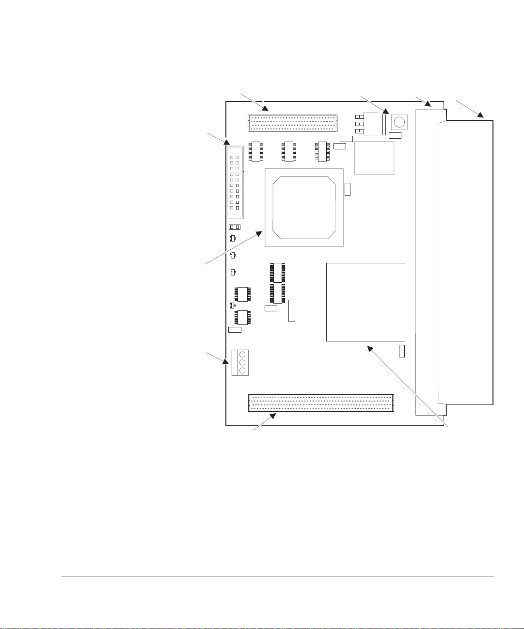
Introduction
Core module/motherboard
connectors HDRB
Multi-ICE
connector
Processor
core
Power
connector
Reset button DIMM socket
SDRAM DIMM
ARM DUI 0125A
Core module/motherboard
connectors HDRA
© Copyright ARM Limited 1999. All rights reserved.
Memory controller and
system bus bridge (FPGA)
Figure 1-1 Integrator/CM940T layout
1-3
Page 16
Introduction
1.2 ARM Integrator/CM940T overview
The major components on the core module are as follows:
• ARM940T microprocessor core
• core module FPGA which implements:
— SDRAM controller
— system bus bridge
— reset controller
— interrupt controller
— status, con f iguration, and interrupt registers.
• volatile memory comprising:
— up to 256MB of SDRAM (optional) via DIMM socket
— 256KB SSRAM.
• SSRAM controller
• clock generator
• system bus connectors
• Multi-ICE debug connector.
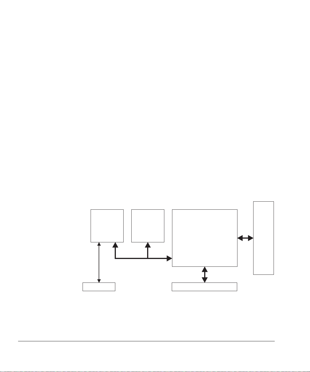
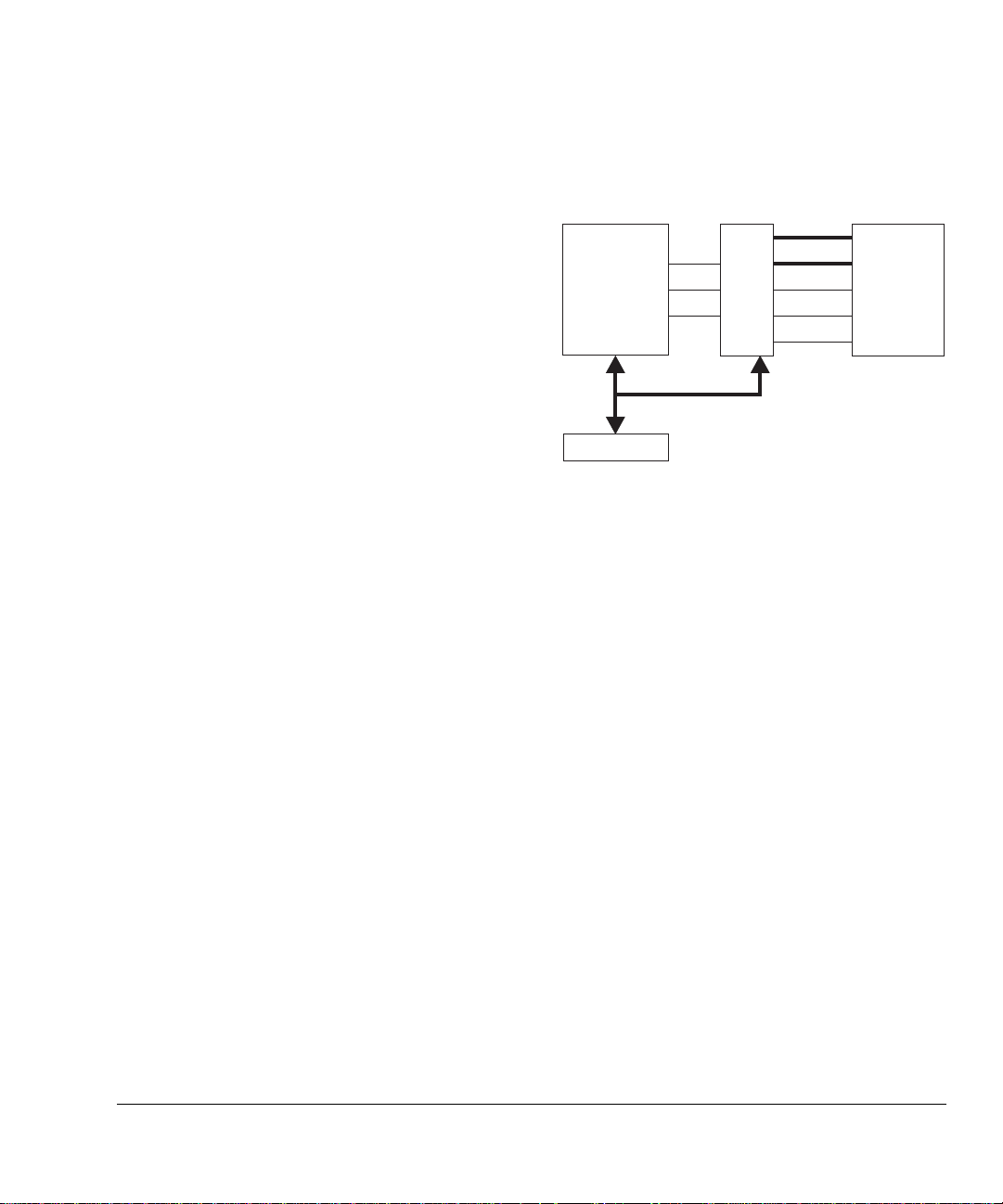
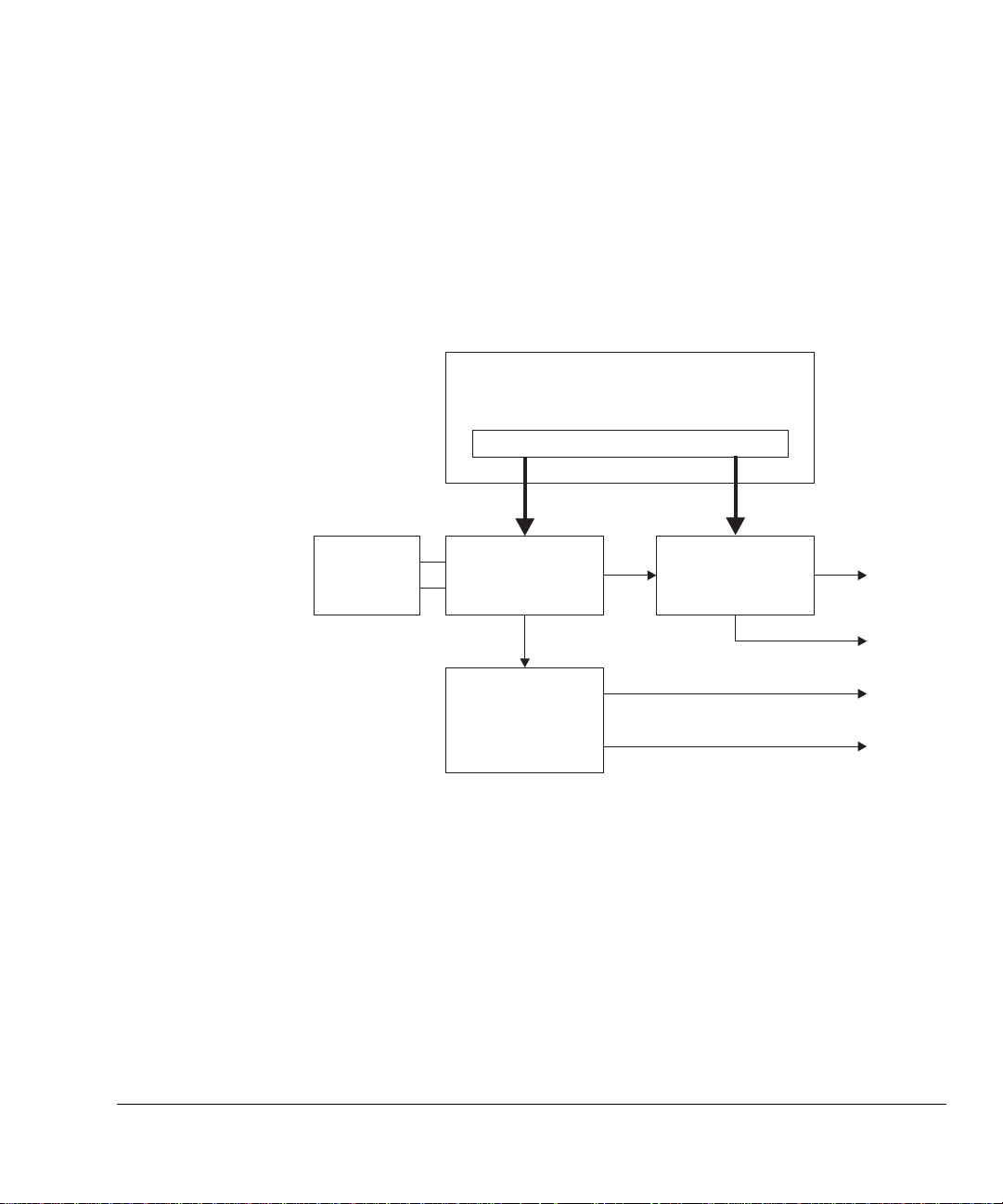
1.2.1 System architecture
1-4
Figure 1-2 illustrates the architecture of the core module.
ARM core
Multi-ICE
© Copyright ARM Limited 1999. All rights reserved.
SSRAM
FPGA
System bus connectors
Figure 1-2 ARM Integrator/CM940T block diagram
SDRAM
ARM DUI 0125A
Page 17

1.2.2 Core module FPGA
The FPGA provides system control functions for the core module, enabling it to operate
as a standalone development system or attached to a motherboard. These functions are
outlined in this section and descri bed in detail in Chapter 3 Hardware Description.
SDRAM controller
The SDRAM controller is implemented within the FPGA. This provides support for
Dual In-line Memory Modules (DIMMs) with a capacity of between 16 and 256MB.
See SDRAM controller on page 3-6.
Reset controller
The reset controller initializes the core and allows the core module to be reset from five
sources:
• reset button
• motherboard
• other core modules
• Multi-ICE
• software.
Introduction
ARM DUI 0125A
For information about the reset controller, see Reset controller on page 3-8.
System bus bridge
The system bus bridge provides an interface between the memory bus on the core
module and the system bus on a motherboard. It allows the local processor access to
interface resources on the motherboard and to the SDRAM on other core modules. It
also allows access to the local SDRAM from the PCI bridge on the motherboard and
processors on other core modules (see System bus bridge on page 3-11).
© Copyright ARM Limited 1999. All rights reserved.
1-5
Page 18

Introduction
Status and configuration space
The status and configuration space contains status and configuration registers for the
core module. These provide the following information and control:
• type of processor and whether it has a cache, MMU, or protection unit
• the position of the core module in a multi-module stack
• SDRAM size, address configuration, and CAS latency setup
• core module oscillator setup
• interrupt control for the processor debug communications channel.
The status and control registers can only be accessed by the local processor. For more
information about the status and control registers see Chapter 4 Programmer’ s
Reference.
1.2.3 Volatile memory
The volatile memory system includes an SSRAM device, and a plug-in SDRAM
memory module (referred to as local SDRAM when it is on the same core module as
the processor). These areas of memory are closely coupled to the processor core to
ensure high performance. Th e cor e mo dul e u ses s eparate memory and system buses to
avoid memory access performance being degraded by bus loading.
The SDRAM controller is implemented within the core module controller FPGA and a
separate SSRAM controller is implemented with a Programmable Logic Device (PLD).
The SDRAM can be accessed by the local processor, by processors on other core
modules, and by other system bus masters.
The SSRAM can only be accessed by the local processor.
1.2.4 Clock generator
The core module uses two on-board clocks:
• CPU clock up to 160MHz
• memory bus clock up to 66MHz.
These clocks are supplied by two clock generator chips. Their frequencies are selected
via the oscillator control register (CM_OSC) within the FPGA. A reference clock is
supplied to the two clock generators and to the FPGA (see Clock generators on
page 3-17). The memory bus and system bus are asynchro nous. This allows each bus to
be run at the speed of its slowest device without compromising the performance of othe r
buses in the system.
1-6
© Copyright ARM Limited 1999. All rights reserved.
ARM DUI 0125A
Page 19

1.2.5 Multi-ICE connector
The Multi-ICE connector enables JTAG hardware debugging equipment, such as
Multi-ICE, to be connected to the core module. It is possible to bo th drive and sense the
system-reset line (nSRST), and to drive JTAG reset (nTRST) to the core from the
Multi-ICE connector. See Multi-ICE su pport on page 3-21.
JTAG test equipment supplied by other vendors may also be used.
Introduction
Note
ARM DUI 0125A
© Copyright ARM Limited 1999. All rights reserved.
1-7
Page 20
Introduction
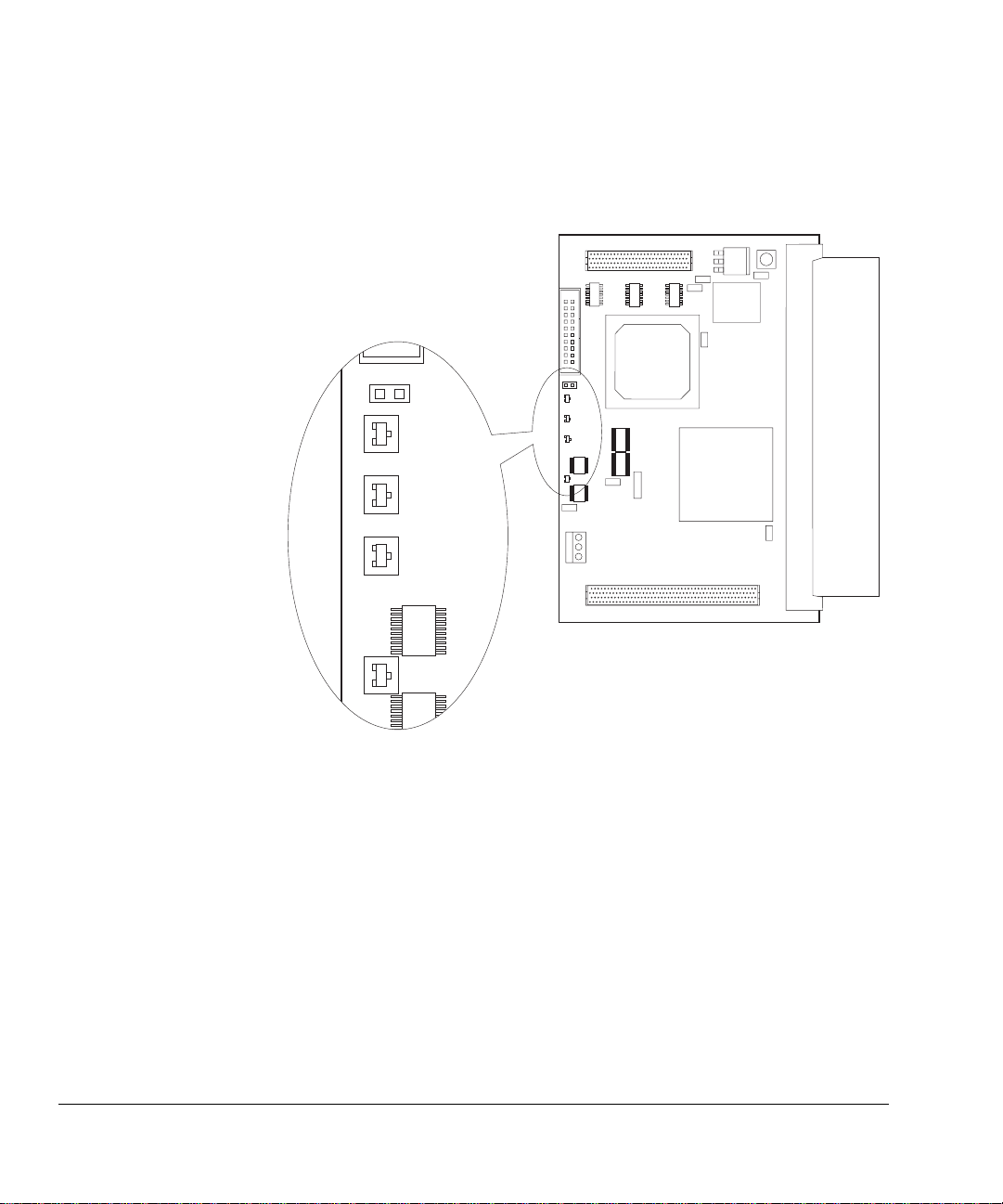
1.3 Links and indicators
The core module provides one link and four surface-mounted LEDs. These are
illustrated in Figure 1-3.
CONFIGMISCFPGA OKPOWERCFGLED
1.3.1 CONFIG link
1-8
Figure 1-3 Links and indicators
The core module has only one link, marked CONFIG. This is left open during normal
operation. It is only fitted when downloading new FPGA and PLD configuration
information.
© Copyright ARM Limited 1999. All rights reserved.
ARM DUI 0125A
Page 21

1.3.2 LED indicators
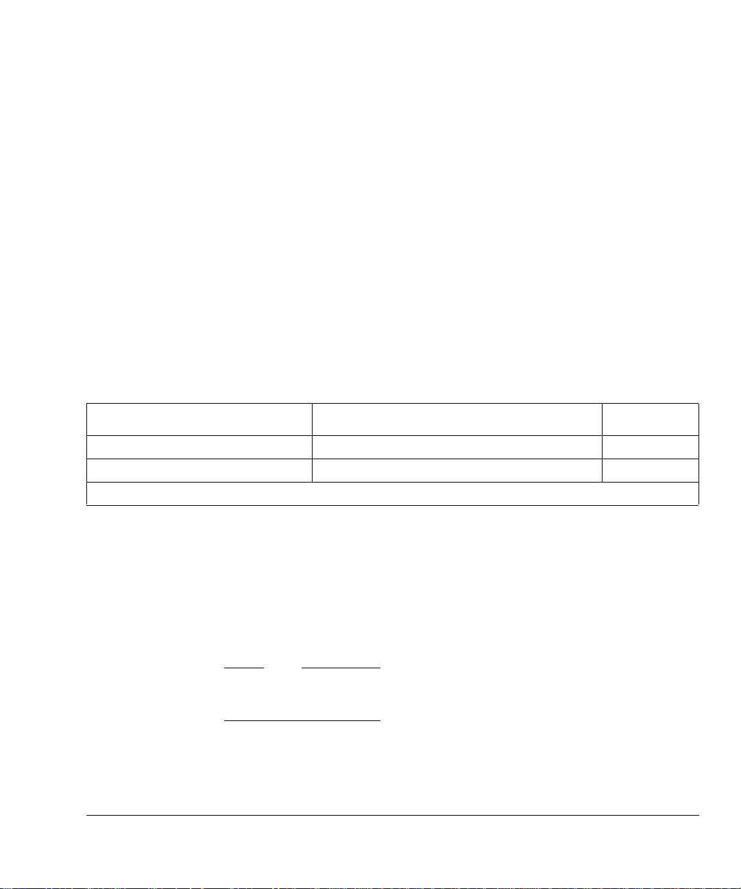
The functions of the four surface-mounted LEDs are summarized in Table 1-1.
Introduction
Table 1-1 LED functional summary
Name Color Function
MISC Green This LED is controlled via the control regi ster (see
CM_CTRL (0x1000000C) on page 4-11).
FPGA OK Green This LED illuminates when the FPGA has successfully
loaded its configuration information following power-on.
POWER Green This LED illuminates to indicate that a 3.3V supply is
present.
CFGLED Orange This LED illuminates to indicate that the CONFIG link is
fitted.
ARM DUI 0125A
© Copyright ARM Limited 1999. All rights reserved.
1-9
Page 22
Introduction
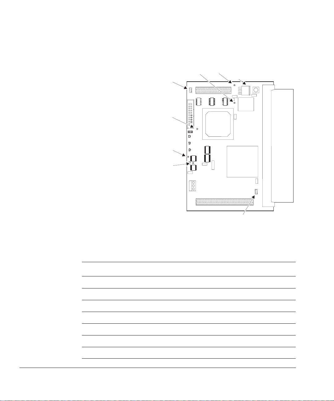
1.4 Test points
The core module provides two ground and five signal test points as an aid to debug.
These are illustrated in Figure 1-4.
Voltage
regulator
TP1
TP3
TP5
TP4
TP6
TP7
1-10
TP2
Figure 1-4 Test points
The functions of the test points are summarized in Table 1-2.
Table 1-2 Test point functions
T est point Name Function
TP1 GND Ground
TP2 GND Ground
TP3 FCLKOUT Clock output from the ARM940T microprocessor core
TP4 LBCLK Local memory bus clock
TP5 Core clock Clock suppl ied to the ARM940T microprocessor core
TP6 VDD940T Output from voltage regulator
TP7 ADJ ADJ pin of voltage regulator
© Copyright ARM Limited 1999. All rights reserved.
ARM DUI 0125A
Page 23

1.5 Precautions
This section contains safety information and advice on how to avoid damage to the core
module.
1.5.1 Ensuring safety
To avoid a safety hazard, only Safety Extra Low Voltage (SELV) equipment should be
connected to the JTAG interface.
1.5.2 Preventing damage
The core module is intended for use within a laboratory or engineering development
environment. It is supplied without an encl osure which leaves the board sensitive to
electrostatic discharges and allows electromagnetic emissions.
To avoid damage to the board you should observe the following precautions.
Introduction
Warning
Caution
ARM DUI 0125A
• Never subject the board to high electrostatic potentials.
• Always wear a grounding strap when handling the board.
• Only hold the board by the edges.
• Avoid touching the component pins or any other metallic element.
• Do not use the board near equipment which could be:
— sensitive to electrom a gnetic emissions (such as medical equipment)
— a transmitter of electromagnetic em issions.
© Copyright ARM Limited 1999. All rights reserved.
1-11
Page 24

Introduction
1-12
© Copyright ARM Limited 1999. All rights reserved.
ARM DUI 0125A
Page 25

Chapter 2
Getting Started
This chapter describes how to set up and prepare the ARM Integrator/CM940T core
module for use. It contains the following sections:
• Setting up a standalone ARM Integrator/CM940T on page 2-2
• Attaching the ARM Integrator/CM9 40T to a motherboard on page 2-5.
ARM DUI 0125A
© Copyright ARM Limited 1999. All rights reserved.
2-1
Page 26

Getting Started
2.1 Setting up a standalone ARM Integrator/CM940T
To set up the core module as a standalone development system:
1. Optionally, fit an SDRAM DIMM.
2. Supply power.
3. Connect Multi-ICE.
2.1.1 Fitting an SDRAM DIMM
You should fit the following type of SDRAM module:
• PC66- or PC100-compliant 168pin DIMM
• unbuffered
• 16MB, 32MB, 64MB, 128MB or 256MB.
To install an SDRAM DIMM:
1. Ensure that the core module is powered down.
2. Op en the SDRAM retaining latches outwards.
3. Press the SDRAM module into the edge connector until the retaining latches
click into place.
Note
The DIMM edge connector has polarizing notches to ensure that it is correctly oriented
in the socket.
2.1.2 Using the core module without SDRAM
The core module can be operated without SDRAM because it has 256KB of SSRAM
permanently fitted. However, in order to operate the core module with ARM deb uggers,
you must change the internal variable
0x00080000 (= 512KB) to 0x00040000 (= 256KB) before running programs that are
linked with the standard libraries.
For further information about ARM debugger internal variables, refer to the Software
Development Toolkit Reference Guide.
2-2
© Copyright ARM Limited 1999. All rights reserved.
$top_of_memory from the default setting of
ARM DUI 0125A
Page 27
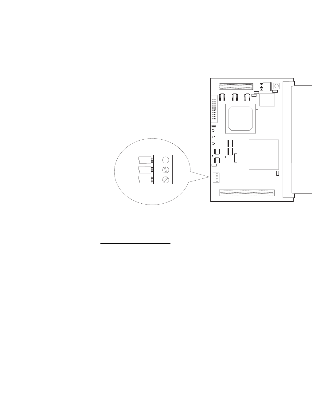
2.1.3 Supplying power
When using the core modul e as a s tandal on e de vel opm ent s yst em, y ou sho ul d conn ect
a bench power supply with 3.3V and 5V outputs to the power connector, as illustrated
in Figure 2-1.
Getting Started
5V
3.3V
GND
5V
3V3
GND
Figure 2-1 Power connector
Note
This power connection is not required when the core module is fitted to a motherboard.
ARM DUI 0125A
© Copyright ARM Limited 1999. All rights reserved.
2-3
Page 28
Getting Started
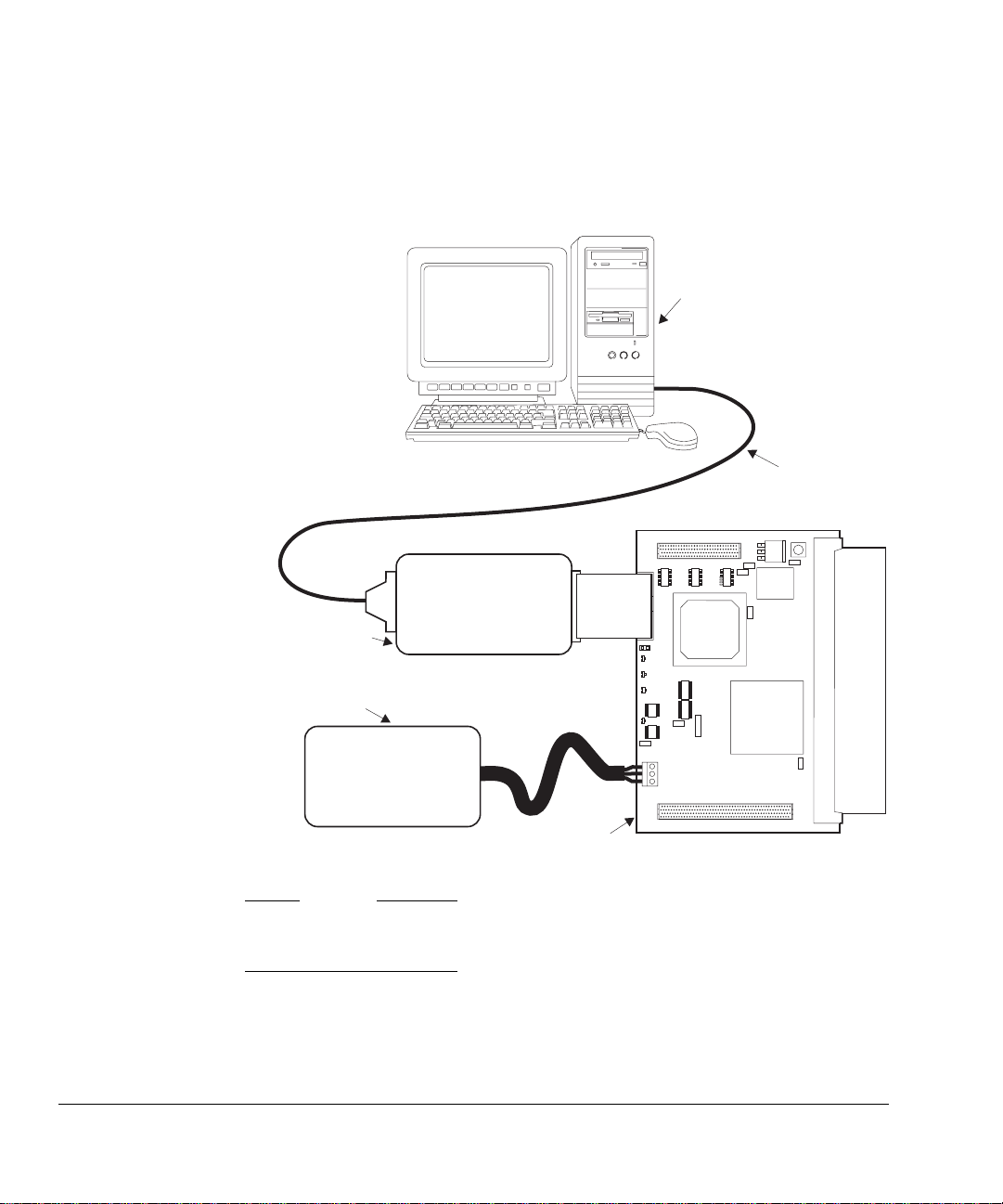
2.1.4 Connecting Multi-ICE
When you are using the core module as a standalone system, Multi-ICE debugging
equipment can be used to download programs. The Multi-ICE setup for a standalone
core module is shown in Figure 2-2.
Multi
Multi-ICE
server/debugger
Parallel
cable
ICE
2-4
Multi-ICE unit
Power supply
Core module
Figure 2-2 Multi-ICE connection to a core module
Caution
Because the core module does not provide non-volatile memory, programs are lost
when the power is removed.
Multi-ICE can also be used when a core module is attached to a motherboard. If more
than one core module is attached, then the Multi-ICE unit must b e connected to the
module at the top of the stack. The Multi-ICE server and the debugger can be on one
computer or on two networked co mputers.
© Copyright ARM Limited 1999. All rights reserved.
ARM DUI 0125A
Page 29
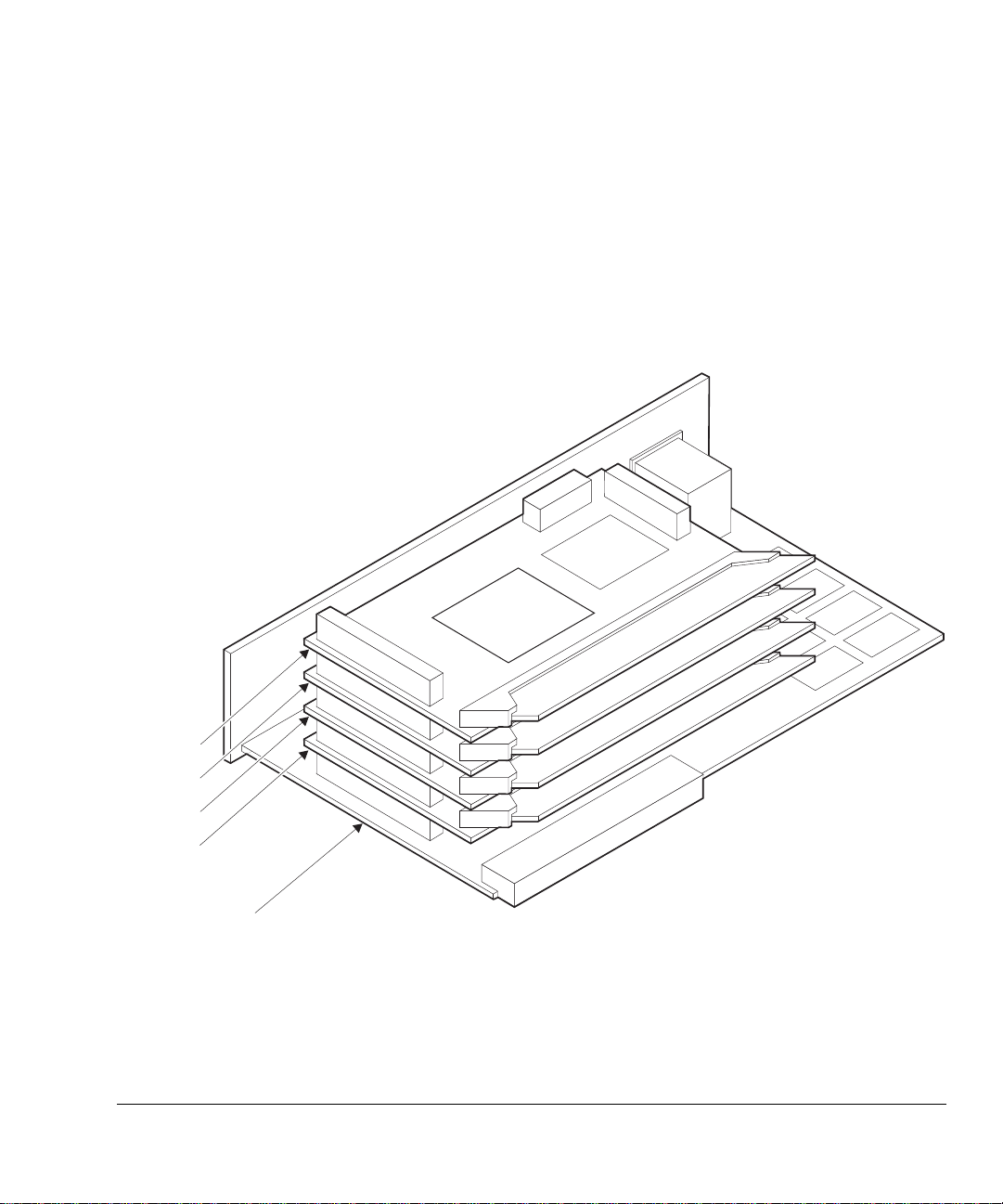
2.2 Attaching the ARM Integrator/CM940T to a motherboard
Attach the core module onto a motherboard (for example, the ARM Integrator/SP) by
engaging the connectors HDRA and HDRB on the bottom of the core module with the
corresponding connectors on the top of the motherboard. The lower side of the core
module has sockets and the upper side of the core module has plugs to allow core
modules to be mounted on t op of one anot her. A maximum of f our core module s can be
stacked on a motherboard.
Figure 2-3 illustrates an example development system with four core modules attached
to an ARM Integrator/SP motherboard.
Getting Started
Module 3
Module 2
Module 1
Module 0
Motherboard
ARM DUI 0125A
Figure 2-3 Assembled Integrator system
© Copyright ARM Limited 1999. All rights reserved.
2-5
Page 30

Getting Started
2.2.1 Core module ID
The ID of the core module is configured automatically by the connectors (there are no
links to set) and depends on its p osition in the stack:
• core module 0 is installed first
• core module 1 is installed next, and cannot be fitted without core module 0
• core module 2 is installed next, and cannot be fitted without core module 1
• core module 3 is installed next, and cannot be fitted without core module 2.
The ID of the core module also defines the ID of the microprocessor it carries and the
system bus address of its SDRAM. The position of a core module in the stack can be
read from the CM_STAT register. See CM_STAT (0x10000010) on page 4-12.
2.2.2 Powering the assembled Integrator development system
Power the assembled Integrator development system by:
• connecting a bench power supply to the motherboard
• installing the motherboard in a card cage or an AT X-type PC case, depending on
type.
For further information, refer to the user guide for the motherboard you are using.
2-6
© Copyright ARM Limited 1999. All rights reserved.
ARM DUI 0125A
Page 31

Chapter 3
Hardware Description
This chapter describes the on-board hardware. It contains the following sections:
• ARM940T microprocessor core on page 3-2
• SSRAM control le r on page 3-3
• Core module FPGA on page3-4
• SDRAM controller on page 3-6
• Reset control l er on page 3-8
• System bus bridge on page 3-11
• Clock generators on page 3-17
• Multi-ICE su ppo rt on page 3-21.
ARM DUI 0125A
© Copyright ARM Limited 1999. All rights reserved.
3-1
Page 32

Hardware Description
3.1 ARM940T microprocessor core
The ARM940T cached processor macrocell is a member of the ARM9 Thumb family
of high-performance 32-bit system-on-a-chip processors. It provides the following:
• ARM9TDMI RISC integer CPU
• 4KB instruction and data caches
• write buffer
• protection unit
• AMBA ASB bus interface.
The ARM940T processor employs a Harvard cache architecture, and so has separate
4KB instruction and 4KB data caches. Each cache has a 4-word line length.
The protection unit allows eight regions of memory to be defined, each with individual
cache and write buffer configurations and access permissions.
The cache system is software-configurable to provide highest average performance or
to meet the needs of real-time systems. Software configurable options include:
• random or round-robin cache line replacement algorithm
• write-through or writeback cache operation
• cache locking with granularity
1
/64 th of cache size.
3-2
The caches and write buffers improve CPU performance and minimize accesses to
off-chip memory, thus reducing overall system power consumption. The ARM940T
includes support for coprocessors, allowing a floating point unit or other
application-specific hardware acceleration to be added.
The ARM9TDMI core executes both the 32-bit ARM and 16-bit Thumb instruction
sets, allowing you to trade between high performance and high code density. It is
binary-compatible with ARM7TDMI, ARM10T DMI, and StrongARM pr ocessors, and
is supported by a wide range of tools, operating systems, and application software.
The ARM940T also features a TrackingICE mode which allows an approach similar to
a conventional ICE mode of operation.
For more information about the ARM940T, refer to the ARM940T Technical Refe rence
Manual.
© Copyright ARM Limited 1999. All rights reserved.
ARM DUI 0125A
Page 33

3.2 SSRAM controller
The SSRAM controller is implemented in a Xilinx 9572 PLD which enables the
SSRAM to achieve single-cycle operation. In addition to controlling accesses to the
SSRAM, the controller generates the processor response signals (BWAIT, BERROR,
BLAST) for all accesses to:
•SSRAM
•SDRAM
• status and configuration register space
• system bus bridge.
Hardware Description
ARM DUI 0125A
© Copyright ARM Limited 1999. All rights reserved.
3-3
Page 34
Hardware Description
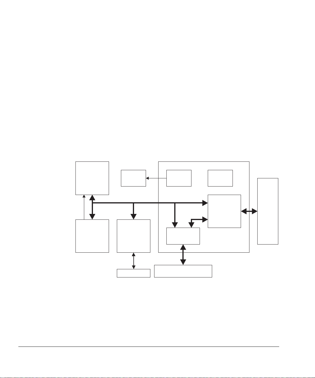
3.3 Core module FPGA
The core module FPGA contains five main functional blocks:
• SDRAM controller on page 3-6
• Reset controller on page 3-8
• System bus bridge on page 3-11
• Core module registers on page 4-7
• Debug interrupt controller, see Debug communications interrupts on page 3-27.
The FPGA provides sufficient functionality for the core module to operate as a
standalone development system, although with limited capabilities. Sy stem bus
arbitration, system interrupt control, and input/output resources are provided by the
system controller FPGA on the motherboard. See the user guide for your mother boar d
for further information.
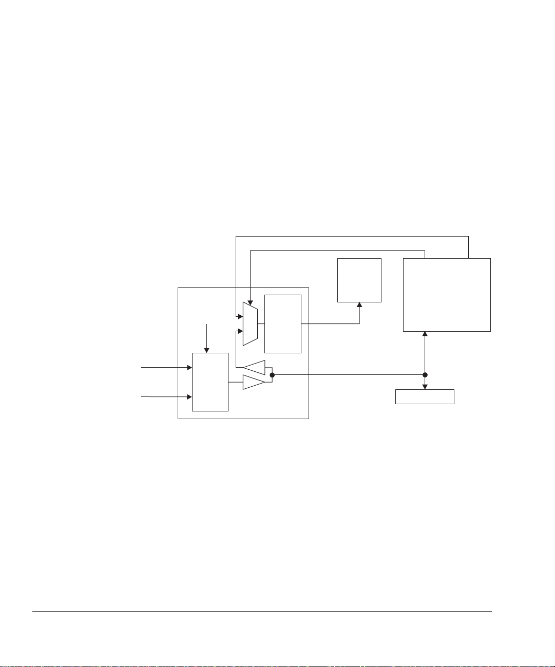
Figure 3-1 illustrates the function of the core module FPGA and shows how it connects
to the other devices in the system.
SSRAM
SSRAM
controller
(PLD)
generator
Memory bus
ARM core
Multi-ICE
Clock
Status/
control
registers
System bus
bridge
System bus
System bus connectors
HDRA/HDRB
Figure 3-1 FPGA functional diagram
Reset
controller
SDRAM
controller
FPGA
SDRAM
3-4
© Copyright ARM Limited 1999. All rights reserved.
ARM DUI 0125A
Page 35
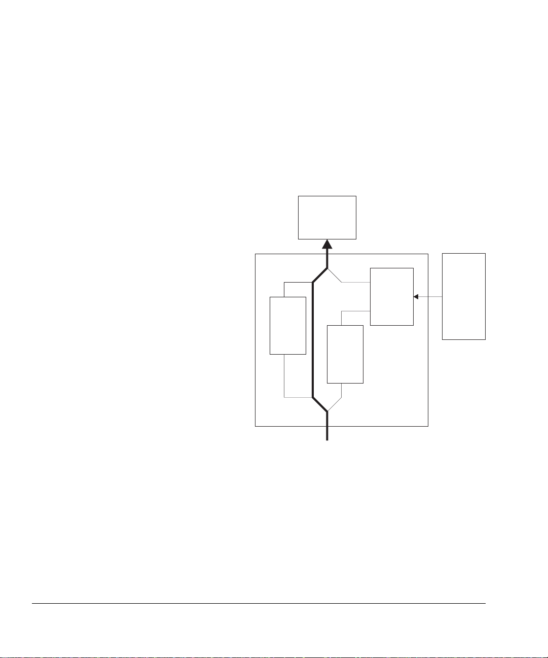
Hardware Description
At power-up the FPGA loads its configuration data from a flash memory device.
Parallel data from the flash is serialized by the Programmable Logic Device (PLD) into
the configuration inputs of the FPGA. Figure 3-2 shows the FPGA configuration
mechanism.
A[18:0]
D[7:0]
OE
WE
CS
FPGA
configuration
ROM
(flash)
FPGA
Multi-ICE
DIN
CCLK
DONE
PLD
Figure 3-2 FPGA configuration
Multi-ICE can be used to reprogram the PLD, FPGA, and flash when the core module
is placed in configuration mode. See Multi-ICE support on page 3-21.
ARM DUI 0125A
© Copyright ARM Limited 1999. All rights reserved.
3-5
Page 36

Hardware Description
3.4 SDRAM controller
The core module provides support for a single 16, 32, 64, 128, or 256MB SDRAM
DIMM.
3.4.1 SDRAM operating mode
The operating mode of the SDRAM devices is controlled with the mode set register
within each SDRAM. These registers are set immediately after power-up to specify:
• a burst size of four for both reads and writes
• Column Address Strobe (CAS) latency of 2 cycles.
The CAS latency and memory size can be reprogrammed via the SDRAM control
register (CM_SDRAM) at address 0x10000020. See CM_SDRAM (0x10000020) on
page 4-14.
Note
Before the SDRAM is used it is necessary to read the SPD memory and program the
CM_SDRAM register with the para meters indicated in Table 4-8 on pag e 4-14. If these
values are not correctly set then SDRAM accesses may be slow or unreliable.
3.4.2 Access arbitration
The SDRAM controller provides two ports to support reads and writes by the local
processor core and by masters on the motherboard. The SDRAM controller uses an
alternating priority scheme to ensure that the processor core and motherboard have
equal access (see System bus bridge on page 3-11).
3.4.3 Serial presence detect
JEDEC-compliant SDRAM DIMMs incorporate a Serial Presence Detect (SPD)
feature. This comprises a 2048-bit serial EEPROM located on the DIMM with the first
128 bytes programmed by the DIMM manufacturer to identify the following:
• module type
• memory organization
• timing parameters.
The EEPROM clock (SCL) operates at 93.75kHz (24MHz divided by 256). The t ransfer
rate for read accesses to the EEPROM is 100kbit/s maximum. The data is read out
serially 8 bits at a time, preceded by a start bit and followed by a stop bit. This makes
reading the EEPROM a very slow process because it takes approximately 27ms to read
all 256 bytes. However, during power-up the content s of the EEPROM are copied into
3-6
© Copyright ARM Limited 1999. All rights reserved.
ARM DUI 0125A
Page 37

Hardware Description
a 64 x 32-bit area of memory (CM_SPD) within the SDRAM controller. The SPD flag
is set in the SDRAM control register (CM_SDRAM) when the SPD data is available.
This copy can be randomly accessed at 0x10000100 to 0x100001FC (see CM_SPD
(0x10000100 to 0x100001FC) on page 4-16).
Write accesses to the SPD EEPROM are not supported.
ARM DUI 0125A
© Copyright ARM Limited 1999. All rights reserved.
3-7
Page 38
Hardware Description
3.5 Reset controller
The core module FPGA incorporates a reset controller which enables the core module
to be reset as a standalone u nit or as part of an Integrator de velopment syst em. The core
module can be reset from five sources:
• reset button
• motherboard
• other core modules
• Multi-ICE
• software.
Figure 3-3 shows the architecture of the reset controller.
nSYSRST
nMBDET
PBRST
nDONE
SWRST
Reset
control
Core
Motherboard
and other
core modules
0
Sync
1
BnRES_M
nSRST
Multi-ICE
FPGA
Figure 3-3 Core module reset controller
3-8
© Copyright ARM Limited 1999. All rights reserved.
ARM DUI 0125A
Page 39

Hardware Description
3.5.1 Reset signals
Table 3-1 describes the external reset signals.
Table 3-1 Reset signal descriptions
Name Description Type Function
BnRES_M Processor r eset Out put The BnRES_M signal is used to reset the processor core. It is
generated from nSRST LOW when the core module is used
standalone, or n SYSRS T LOW when the core module is
attached t o a motherboard.
It is asserted as soon as the appropriate input becomes active.
It is deasserted synchronously from the falling edge of the
processor bus clock.
nDONE FPGA config ured Input The nDONE signal is an inversion of the open collector
signal FPGADONE which is generated by all FPGAs when
they have completed their configuration. The FPGADONE
signal is routed round the system through the HDRB
connectors to the inputs of all other FPGAs in the system. The
signal nSRST is held asserted until nDONE is driven LOW.
nMBDET Motherboard detect Input The nMBDET signal is pulled LOW when the core module is
attached to a motherboard and HIGH when the core module is
used standalone.
When MBDET is LOW, nSYSRST is used to generate the
BnRES_M signal.
When nMBDET is HIGH, nSR ST is used to genera te the
BnRES_M signal.
PBRST Push-button reset Input The PBRST signal is generat ed by pressing the reset button.
nSRST System reset Bidirectional The nSRST open collector output signal is driven LOW by
the core module FPGA when the signal PBRST or software
reset (SWRST) is asserted.
As an input, nSRST can be driven LOW by Multi-ICE.
If there is no motherboard present, the nSRST signal is
synchronized to the processor bus clock to generate the
BnRES-M signal.
nSYSRST System reset Input The nSYSRST signal is generated by the system controller
FPGA on the motherboard. It is used to generate the
BnRES_M signal when the core module is attach ed to a
motherboard. It is selected by the motherboard detect signal
(nMBDET).
ARM DUI 0125A
© Copyright ARM Limited 1999. All rights reserved.
3-9
Page 40

Hardware Description
3.5.2 Software resets
The core module FPGA provides a software reset which can be trigg ered by writi ng to
the reset bit in the CM_CTRL register. This generates the internal reset signal SWRST
which generates nSRST and resets the whole system (see C M_CTRL ( 0x1000000C) on
page 4-11).
3-10
© Copyright ARM Limited 1999. All rights reserved.
ARM DUI 0125A
Page 41

3.6 System bus bridge
The system bus bridge provides an asynchronous bus interface between the local system
bus and system bus connecting the motherboard and other modules.
Inter-module accesses are supported by two 16 x 74-bit FIFOs. Each of the 16 entries
in the FIFOs contains:
• 32-bit data used for write transfers
• 32-bit address used for reads and writes
• 10-bit transaction control used for reads and writes.
3.6.1 Processor accesses to the system bus
The first FIFO supports read and write accesses by the local processor to the system b us,
which extends onto the motherboard and other modules.
Processor writes
The data routing for processor writes to the system bus is illus trat ed in Figure 3-4.
Hardware Description
Processor
core
ARM DUI 0125A
FIFO
FIFO
Motherboard
Figure 3-4 Processor writes to the system bus
© Copyright ARM Limited 1999. All rights reserved.
SDRAM
controller
SDRAM
3-11
Page 42
Hardware Description
Write transactions from the processor to the system b us normally complete on the local
memory bus in a single cycle. The data, address, and control information associated
with the transfer are posted into FIFO, and the transfer on the system bus occurs some
time later when that bus is available. This means that system bus error responses to
write transfers are not reported back to the pro cessor as data aborts. If the FIFO is full,
the processor receives a wait response until space becomes available.
Processor reads
The data routing for processor reads from the system bus is illu strated in Figure 3-5.
Processor
core
SDRAM
controller
FIFO
FIFO
Motherboard
Figure 3-5 Processor reads from the system bus
SDRAM
For reads from the system bus, the address and control information also pass through
the FIFO. The returned data from the system bus bypasses the FIFO.
The order of processor transactions is preserved on the system bus. Any previously
posted writes are drained from the FIFO (that is, completed on the system bus) before
the read transfer is performed. The processor receives a wait response until the read
transfer has completed on the system bus, when it receives the data an d any associated
bus error response from the system bus. For information about SDRAM addresses, see
SDRAM accesses on page 4-4.
3-12
© Copyright ARM Limited 1999. All rights reserved.
ARM DUI 0125A
Page 43

3.6.2 Motherboard accesses to SDRAM
The second FIFO supports read and write accesses by system bus masters on the
motherboard and other core modules to the local core module memory.
System bus writes
The data routing for system bus writes to SDRAM is illustrated in Figu re 3-6.
Hardware Description
Processor
core
SDRAM
controller
FIFO
FIFO
Motherboard
SDRAM
Figure 3-6 System bus writes to SDRAM
Write transactions from the system bus to the SDRAM normally complete in a single
cycle on the system bus. The data, address, and control information associated with the
transfer are posted into the FIFO, and the transfer into the SDRAM completes when th e
SDRAM is available. If the FIFO is full, then the system bus master receives a retract
response indicating that the arbiter may grant the bu s to another master and that this
transaction must be retried later.
ARM DUI 0125A
© Copyright ARM Limited 1999. All rights reserved.
3-13
Page 44

Hardware Description
System bus reads
The data routing for system bus reads from SDRAM is illustrated in Figure 3-7.
Processor
core
For system bus reads, the address and control information also pass through the FIFO,
but the returned data from the SDRAM bypasses the FIFO.
The order of transactions on the system bus and the memory bus is preserved. Any
previously posted write transactions are dr ained from the FIFO (that is, writes to
SDRAM are completed) before the read transfer is performed.
3.6.3 Multiprocessor
The two FIFOs operate independently, as described above, and can be accessed at the
same time. This makes it possible for a local processor to read local SDRAM via the
system bus (through both FIFOs). This feature can be used to support multiprocessor
systems that share data in SDRAM because the processors can all access the same
DRAM locations at the same addresses.
SDRAM
controller
FIFO
FIFO
Motherboard
Figure 3-7 System bus reads from SDRAM
SDRAM
3-14
© Copyright ARM Limited 1999. All rights reserved.
ARM DUI 0125A
Page 45
3.6.4 System bus signal routing
The core module is mounted onto a motherboard via the connectors HDRA and HDRB.
As well as carrying all signal connections between the boards, these provide mech anical
mounting (see Attaching the ARM Integrator/CM920T to a motherboa rd on page 2-5).
HDRA
The signals on the HDRA connectors are tracked between the socket on the underside
and the plug on the top so that pi n 1 conn ects to pi n 1, pin 2 to pi n 2 and so on. That is,
the signals are routed straight through.
HDRB
A number of signals on the HDRB connectors are rotated i n groups of four between the
connectors on the bottom and top of each module. This ensures that each processor (or
other bus master device) on a module connects to the correct signals according to
whether it is bus master 0, 1, 2, or 3. The ID for the bus master on a module is
determined by the position of the module in the stack.
This signal rotation scheme is illu strated in Figure 3-8.
Hardware Description
Module 3
Module 2
Module 1
Module 0
Motherboard
ARM DUI 0125A
D
C
C
B
B
A
A
D
DCB A
C
B
B
A
A
D
D
C
B
A
A
D
D
C
C
B
Figure 3-8 Signal rotation on HDRB
© Copyright ARM Limited 1999. All rights reserved.
A
D
D
C
C
B
B
A
To on-board
devices
3-15
Page 46

Hardware Description
The example in Figure 3-8 illustrates how a group of four signals (labelled A, B, C, and
D) are routed through a group of four con nector pins u p through the s tack. It highligh ts
how signal C is rotated as it passes up through the stack and only utilized on module 2.
All four signals are rotated and utilized in a similar way, as follows :
• signal A on core module 0
• signal B on core module 1
• signal C used on core module 2
• signal D used on core module 3.
For details of the signals on the HDRB connectors, see HDRB on page A-4.
Note
The JTAG signals are discussed in Multi-ICE support on page 3-21.
3.6.5 Bus operating modes
The bus operating modes are programmed by writing to coprocessor 15 register 1 within
the ARM940T microprocessor core.
The Integrator system supports:
• asynchronous and FastBus clocking
• little-endian addressing.
3-16
The Integrator system does not support:
• synchronous clocking
• big-endian addressing.
For details of how to set the bus operating parameters, refer to the ARM940T Technical
Reference Manual.
© Copyright ARM Limited 1999. All rights reserved.
ARM DUI 0125A
Page 47
3.7 Clock generators
The core module provides its own clock generators and operates asynchronously with
the motherbo ard. The clock generator provides two programmable cloc ks:
• processor core clock CORECLK
• processor local memory bus clocks LCLK and nLCLK.
In addition, a fixed-frequency reference clock REFCLK is supplied to the FPGA.
These clocks are supplied by two MicroClock ICS525 devices and by the SSRAM
controller PLD, as illustrated in Figure 3-9.
Hardware Description
FPGA
CM_OSC register
24MHz
crystal
ICS525
(U6)
2XCLK
ICS525
(U7)
REFCLK
CORECLK
LCLK
SSRAM controller
(PLD)
nLCLK
Figure 3-9 Core module clock generator
The ICS525s are supplied with a reference clock signal from a 24MHz crystal
oscillator. The 2XCLK output from the first ICS525 (U6) is supplied to the PLD and
divided by two to produce the signals LCLK and nLCLK. The output from U7
provides the CORECLK signal. The reference output from U6 supplies the reference
input to U7 and the reference output from U7 supplies the FPGA reference clock.
The output frequencies from the ICS525s are configured using divider input pins to
produce a wide range of frequencies.
ARM DUI 0125A
© Copyright ARM Limited 1999. All rights reserved.
3-17
Page 48

Hardware Description
3.7.1 Processor core clock (CORECLK)
The frequency of CORECLK is controllable in 1MHz steps in the range 12MHz to
160MHz. This is achieved by setting the Voltage Controlled Oscillator (VCO) divider
and output divider for the CORECLK generator via the CM_OSC register. The VCO
divider is controlled b y the C_VDW bi ts and ou tput di vide r is cont rolled by the C _OD
bits. The reference divider value is fixed.
Table 3-2 shows the values placed on the divider input pins and how the clock speeds
are derived. The bits marked:
• C are programmable in the CM_OSC register
• 1 are tied HIGH
• 0 are tied LOW.
Table 3-2 CORECLK divider values
C_RDW R[6:0] C_VDW V[8:0] C_OD S[2:0]
00101100CCCCCCCCCCC
22 (fixed value) 4 – 152 (<4 and >152 not allowed) 2-10
12 – 160MHz in 1MHz steps
3-18
The frequency of CORECLK can be derived from the formula:
freq = 2*((C_VDW+ 8)/C_OD)
where:
C_VDW is the VCO divider word for the core clock.
C_OD is the output divider for the core clock.
For details about programming C_VDW and C_OD, see CM_OSC (0x10000008) on
page 4-9.
Note
Values for C_VDW and C_OD can be calculated using the ICS525 calculator on the
Microclock website.
The CORECLK is buffered with a PI49FCT3805 to convert the Phase-Locked Loop
(PLL) output to 3.3V signal level. The clock is series terminated with a 33Ω resistor and
then drives a single load on the microprocessor core.
© Copyright ARM Limited 1999. All rights reserved.
ARM DUI 0125A
Page 49
3.7.2 Processor bus clocks (LCLK and nLCLK)
The frequency of the processor bus clocks LCLK and nLCLK is determined by the
frequency of 2XCLK. The clock signal 2XCLK is divided by 2 by the SSRAM
controller PLD to produce LCLK and nLCLK.
The frequency of LCLK is controllable in 0.5MHz steps in the range 6MHz to 66MHz.
This is achieved by programming the VCO and output divider bits for the 2XCLK
generator in the CM_OSC regist er. The VCO divi der is co ntroll ed by th e L_VDW bits
and the output divider is controlled by the L_OD bits.The reference divider is fixed.
The maximum speed of 2XCLK is limited by the speed of the SSRAM PLD.
Table 3-3 shows the values placed on the divider input pins and how the clock speeds
are obtained. The bits marked:
• L are programmable in the CM_OSC register
• 1 are tied HIGH
• 0 are tied LOW
L_RDW R[6:0] L_VDW V[8:0] L_OD S[2:0]
.
Hardware Description
Table 3-3 2XCLK divider values
00101100LLLLLLLLLLL
22 (fixed value) 4 – 124 (<4 and >124 not allowed) 2-10
12 – 132MHz in 1MHz steps (for 2XCLK)
The frequency of LCLK can be derived from the formula:
freq = (L_VDW+ 8)/L_OD
where:
L_VDW is the VCO divider word for the processor bus clock.
L_OD is the output divider for the processor bus clock.
Note
Values for L_VDW and L_OD can be calculated using the ICS525 calculator on the
Microclock website.
For details about programming L_VDW and L_OD, see CM_OSC (0x10000008) on
page 4-9.
ARM DUI 0125A
© Copyright ARM Limited 1999. All rights reserved.
3-19
Page 50

Hardware Description
The LCLK clock signal is buffered by a 5-output low-skew buffer PI49FCT3805 to
drive five loads. These are:
• SDRAM_CLK[3:0]
•SSRAM_CLK.
The nLCLK clock signal is a phase-aligned inversion of the LCLK signal. It is
buffered by a 5-output low-skew buffer PI49FCT3805 to four loads. These are:
• ARM_BCLK_M
•PLD_BCLK_M
• FPGA_BCLK_M
•LA_BCLK_M.
All clocks are series terminated with 33Ω resistors placed as close to the source as
possible.
3.7.3 FPGA reference clock (REFCLK)
The REFCLK signal is used by the FPGA to generate the SDRAM refresh clock and
SPD EEPROM clock. This is a fi xed- freq uency clock of 24MHz which is output from
the reference pin of the second ICS525 chip U7.
3-20
© Copyright ARM Limited 1999. All rights reserved.
ARM DUI 0125A
Page 51

3.8 Multi-ICE support
The core module provides support for debug using JTAG. It provides a Multi-ICE
connector and JTAG scan paths aro und the development sys tem. Figure 3-10 sho ws the
Multi-ICE connector and the CONFIG link.
Hardware Description
Multi-ICE connector
CONFIG link
ARM DUI 0125A
CFGLED
Figure 3-10 JTAG connector, CONFIG link, and LED
The CONFIG link is used to enable in-circuit programming of the FPGA and PLDs
using Multi-ICE (see Debugging modes on page 3-23).
The Multi-ICE connector provides a set of JTAG signals allowing third-party JTAG
debugging equipment t o be used (see JTAG si gnals on page 3-24). If you are debugging
a development system with multiple core modules, connect the Multi-ICE hardware to
the top core module.
© Copyright ARM Limited 1999. All rights reserved.
3-21
Page 52
Hardware Description
3.8.1 JTAG scan path
Figure 3-11 shows a simplified diagram of the scan path.
Core module
TDI
Multi-ICE
HDRB
HDRB
TDO
TDI
Processor
core
TDI
nMBDET
Core module
TDO
TDI
Processor
core
HDRB
HDRB
Motherboard
Figure 3-11 JTAG scan path (simplified)
When the core module is used as a standalone development system, the JTAG scan path
is routed through the processor core and back to the Multi-ICE connector.
When the core module is attached to a motherboard, either directly or with other core
modules, the TDI signal from the top core module is routed down through the HDRB
connectors to the motherboard. The path is routed back up the stack through the
processor core on each core module, before being returned to the Multi-ICE connector.
The motherboard detect signal nMBDET signal is used to control the routing for a
standalone or an attached core module.
3-22
The PLDs and FPGAs are included in the scan chain when the core module is in
configuration mode.
© Copyright ARM Limited 1999. All rights reserved.
ARM DUI 0125A
Page 53

3.8.2 Debugging modes
The core module is capable of operating in two modes:
• normal debug mode
• configuration mode.
Normal debug mode
During normal operation and software development, the core module operates in debug
mode. The debug mode is selected by default (when a jumper is not fitted at the
CONFIG link, see Figure 3-10 on page 3-21). In this mode, the processor core and
debuggable devices on other modules are accessible on the scan chain, as shown in
Figure 3-11 on page 3-22.
Configuration mode
In configuration mode the debuggable devices are still accessible and, in addition, all
FPGAs and PLDs in the system are added into the scan chain. This allows the board to
be configured or upgraded in the field using Multi-ICE or other JTAG debugging
equipment.
To select configuration mode, fit a jumper to the CONFIG link on the co re module at
the top of the stack (see Figure 3-10 on page 3-21). This has the effect of pulling the
nCFGEN signal LOW which illuminates the CFG LED (yellow) on each module in the
stack and reroutes the JTAG scan path. The LED provides a warning that the
development system is in the conf iguration mode.
Hardware Description
ARM DUI 0125A
Note
Configuration mode is guaranteed for a single core module attached to a motherboard
but may be unreliable if more than one cor e module is attached. The larger load s on the
TCK and TMS lines may cause unreliable operation.
After configuration or code updates you must:
1. Remove the CONFIG link.
2. Power cycle the development system.
© Copyright ARM Limited 1999. All rights reserved.
3-23
Page 54

Hardware Description
3.8.3 JTAG signals
The configuration mode allows FPGA and PLD code to be updated as follows:
• The FPGAs are volatile, but load their configuration from flash memory. Flash
memory, which itself does not have a JTAG port, can be programmed by loading
designs into the FPGAs and PLDs which hand le the transfer of data to the flash
using JTAG.
• The PLDs are non-volatile devices which can be p rogrammed directly by JTAG.
Figure 3-12 shows the pinout of the Multi-ICE connector and Table 3-4 on page 3-25
provides a description of the JTAG signals.
1192
nTRST
TDI
TMS
TCK
RTCK
TDO
nSRST
DBGRQ
DBGACK
20
3V33V3
GND
GND
GND
GND
GND
GND
GND
GND
GND
Figure 3-12 Multi-ICE connector pinout
Note
In the description in Table 3-4 on page 3-25, the term JTAG equipment refers to any
hardware that can drive the JTAG signals to devices in the scan chain. In most cases this
will be Multi-ICE, although hardware from third-party suppliers can also be used to
debug ARM processors.
3-24
© Copyright ARM Limited 1999. All rights reserved.
ARM DUI 0125A
Page 55

Name Description Function
Hardware Description
Table 3-4 JTAG signal description
DBGRQ Debug request
(from JTAG equipment)
DBGRQ is a request for the processor core to enter the debug
state. It is provided for compatibility with third-party JTAG
equipment.
DBGACK Debug acknowledge
(to JTAG equipment)
DBGACK indicates to the deb ugger that the processor core has
entered debug mode. It is provided for compatibility with
third-party JTAG equipment.
DONE FPGA configured DONE is an open-collector signa l which indicates when FPGA
configuration is complete. Although this signal is not a JTAG
signal, it does effect nSRST. The DONE signal is routed between
all FPGAs in the system through the HDRB connectors. The
master reset controller on the motherboard senses this signal and
holds all the boards in reset (by driving nSRST LOW) until all
FPGAs are configured.
nCFGEN Configuration enable
(from jumper on module at the
top of the stack)
nCFGEN is an active LOW signal used to put the boards into
configuration mode. In configuration mode all FPGAs and PLDs
are connected to the scan chain so that they can be configured by
the JTAG equipment.
nRTCKEN Return TCK enable (from core
module to motherboard)
nRTCKEN is an active LOW signal driven by any core module
that requires RTCK to be routed back to the JTAG equipment. If
nRTCKEN is HIGH, the motherboard drives RTCK LOW. If
nRTCKEN is LOW, th e motherboard drives the TCK signal
back up the stack to the JTAG equipment.
nSRST System reset (bidirectional) nSRST is an active LOW open-collector signal which can b e
driven by the JTAG equipment to reset the target board. Some
JTAG equipment senses this line to determine when a board has
been reset by the user.
The open collector nR S T reset sign al may be driv en LOW by the
reset controller on the core module t o cause the motherboard to
reset the whole system by driving nSYSRST LOW.
This is also used in configuration mode to control the
initialization pin (nINIT) on the FPGAs.
Though not a JTAG signal, nSRST is described because it can be
controlled by JTAG equipment.
nTRST Test reset (from JTAG
equipment)
ARM DUI 0125A
© Copyright ARM Limited 1999. All rights reserved.
This active low open-collector is used to reset the JTAG port and
the associated debug circuitry on the ARM940T processor. It is
asserted at power-up by each module, and can be driven by the
JTAG equipment. This signal is also used in configuration mode
to control the programming pin (nPROG) on FPGAs.
3-25
Page 56

Hardware Description
Name Description Function
Table 3-4 JTAG signal description (continued)
RTCK Return TCK
(to JTAG equipment)
TCK Test clock
(from JTAG equipment)
TDI Test data in
(from JTAG equipment)
Some devices sample TCK (for example a synthesizable core
with only one clock), and this has the effect of delaying the time
at which a component act ually captures data. RTCK is a
mechanism for returning the sampled clock to the JTAG
equipment, so that the clock is not advanced until the
synchronizing de vice captured the dat a . In adaptive clocking
mode, Multi-ICE is required to detect an edge on RTCK before
changing TCK. In a multiple device JT AG chain, the RTCK
output from a component connects to the TCK input of the
down-stream device. The RTCK si gnal on the module
connectors HDRB returns TCK to the JTAG equipment. If there
are no synchronizing components in the scan chain then it is
unnecessary to use the RTCK signal and it is connected to
ground on the motherboard.
TCK synchronizes all JTAG transactions. TCK connects to all
JTAG components in the scan chain. Series termination resistors
are used to reduce reflections and maintain good signal integrity.
TCK flows down the stack of modules and connects to each
JTAG component. However, if there is a device in the scan chain
that synchronizes TCK to some other clock, then all down-stream
devices are connected to the RTCK signal on that component
(see RTCK).
TDI goes down the stack of modules to the motherboard and then
back up the stack, labelled TDO, connecting to each component
in the scan chain.
TDO Test data out
(to JTAG equipment)
TMS Test mode select
(from JTAG equipment)
3-26
TDO is the return path of the data input signal TDI. The module
connectors HDRB have tw o pin s labelled TDI and TDO. TDI
refers to data flowing down the stack and TDO to data flowing up
the stack. The JTAG components are connected in the retu rn p a th
so that the length of track driven by the last compone nt in the
chain is kept as short as possible.
TMS controls transitions in the tap controller state machine.
TMS connects to all JTAG components in the scan chain as the
signal flows down the module stack.
© Copyright ARM Limited 1999. All rights reserved.
ARM DUI 0125A
Page 57

3.8.4 Debug communications interrupts
The ARM940T processor core incorporates EmbeddedICE hardware and provides a
debug communications data register which is used to pass data between the processor
and JTAG equipment. The processor accesses this register as a normal 32-bit read/write
register and the JTAG equipment reads and writes the register using the scan chain. For
a description of the debug communications channel, see the ARM940T Technical
Reference Manual.
Interrupts can be used to signal when data has been written into one side of the register
and is available for reading from the other side. These interrupts are supported by the
interrupt controller within the core module FPGA and can be enabled and cleared by
accessing the interrupt registers (see Interrupt registers on page 4-19).
Hardware Description
ARM DUI 0125A
© Copyright ARM Limited 1999. All rights reserved.
3-27
Page 58

Hardware Description
3-28
© Copyright ARM Limited 1999. All rights reserved.
ARM DUI 0125A
Page 59

Chapter 4
Programmer’s Reference
This chapter describes the memory map and the status and control registers. It contains
the following sections:
• Memory organization on page 4-2
• Exception vector mapping on page 4-6
• Core module reg isters on page 4-7
• Interrupt registers on page 4-19.
ARM DUI 0125A
© Copyright ARM Limited 1999. All rights reserved.
4-1
Page 60

Programmer’s Reference
4.1 Memory organization
This section describes the memory map. For a standalone core module, the memory
map is limited to local SSRAM, SDRAM, and core module registers. For the full
memory map of an Integ rator deve lopment system, which in cludes a mot herboard, y ou
should refer to the user guide for the motherboard.
4.1.1 Core module memory map
The core module has a fixed memory map which maintains compatibility with other
ARM modules and Integrator systems. Table 4-1 shows the memory map.
Table 4-1 ARM Integrator/CM940T memory map
nMBDET REMAP Address range Region size Description
0 0 0x00000000 to 0x0003FFFF 256KB Boot ROM (on motherboard)
0 1 0x00000000 to 0x0003FFFF 256KB SSRAM
1 X 0x000 00000 to 0x0003FFFF 256KB SSRAM
X X 0x00040000 to 0x0FFFFFFF 256MB Local SDRAM
X X 0x10000000 to 0x10FFFF FF 16MB Core module registers
0 X 0x11000000 to 0xFFFFFFFF 4GB to 272MB System bus address space
1 X 0x11000000 to 0xFFFFFFFF 4GB to 272MB Abort
4.1.2 Boot ROM and SSRAM accesses
The boot ROM on the motherboard and the SSRAM on the core module share the same
location within the Integrator memory map. Accesses to either the boot ROM or
SSRAM are controlled by the REMAP bit and the motherboard detect signal
(nMBDET) from the motherboard, as shown in Table 4-1 on page 4-2.
Remap
The REMAP bit only has effect if the core module is attached to a motherboard
(nMBDET=0). It is controlled by bit 2 of the CM_CTRL register at 0x1000000C and
functions as follows:
REMAP=0 As it is after a reset. The Boot ROM on the motherboard appears in the
address range 0x0 to 0x3FFFF.
REMAP=1 The SSRAM appears in the 0x0 to 0x3FFFF address range.
4-2
© Copyright ARM Limited 1999. All rights reserved.
ARM DUI 0125A
Page 61
Programmer’s Reference
Motherboard detect
The nMBDET signal operates as follows:
nMBDET=0 The core module is attached to a motherboard, and accesses in the
address range 0x0 to 0x3FFFF to the boot ROM or SSRAM are
controlled by the REMAP bit.
nMBDET=1 The core module is not attached, and accesses in the address range 0x0 to
0x3FFFF are routed to the SSRAM.
Note
The SSRAM is local, which means that it can only be read by the processor on the same
core module. It provides fast local memory for the local processor and cannot be
accessed by other system bus masters.
4GB
ARM DUI 0125A
Abort
CM registers
SDRAM
SSRAM
Standalone
Motherboard
CM registers
SDRAM
Boot ROM
Attached
(after reset)
Figure 4-1 Effect of remap and motherboard detect
© Copyright ARM Limited 1999. All rights reserved.
Motherboard
CM registers
SDRAM
SSRAM
Attached
(after remap)
272MB
256MB
256KB
4-3
Page 62

Programmer’s Reference
4.1.3 SDRAM accesses
The Integrator memory map provides a 256MB address space for SDRAM. When a
smaller sized SDRAM DIMM is fitted, it is mapped repeatedly to fill the 256MB space.
For example, a 64MB DIMM appears four times, as shown in Figure 4-2.
0x0FFFFFFF
64MB
Local SDRAM
(repeat image)
64MB
Local SDRAM
(repeat image)
64MB
64MB
256KB
Figure 4-2 SDRAM repeat mapping for a 64MB DIMM
Local SDRAM
(repeat image)
Local SDRAM
SSRAM
0x0003FFFF
Local SDRAM
The local processor can access the local SDRAM (that is, the SDRAM on the same core
module) at 0x00000000 to 0x0FFFFFFF in the core module address space. However,
the lowest 256KB (0x00000000 to 0x0003FFFF) is hidden by the SSRAM or boot
ROM, depending upon whether the core mo dule is attached to a motherboard and upon
the state of the REMAP bit.
4-4
The SDRAM cannot be accessed within this address space, although it can be accessed
at one of its repeat images or at its alias location. In the case of a 256MB DIMM which
fills the local SDRAM space, the first 256KB can only be accessed at the alias location
(see System bus accesses to SDRAM below) .
© Copyright ARM Limited 1999. All rights reserved.
ARM DUI 0125A
Page 63

Programmer’s Reference
System bus accesses to SDRAM
If the core module is mounted on a motherboard, the SDRAM is mapped to appear at
the al iased module memory region of the combine d Integrator system bus memory map .
The SDRAM can be accessed by all bus masters at its alias location, and accessed by
the local processor at both its local and alias locations.
The system bus address for a core module is automatically controlled by its position in
the stack (see Core module ID on page 2-6). Figure 4-3 show s the local and alias
address of the SDRAM on four core modules.
System bus address
All masters
0xBFFFFFFF
0xB0000000
0xAFFFFFFF
0xA0000000
0x9FFFFFFF
0x90000000
0x8FFFFFFF
0x80000000
Local address
0x0FFFFFFF
SDRAM
core module 3
0x00000000
0x0FFFFFFF
SDRAM
core module 2
0x00000000
0x0FFFFFFF
SDRAM
core module 1
0x00000000
0x0FFFFFFF
SDRAM
core module 0
0x00000000
Figure 4-3 Core module local and alias addresses
Module 3
Module 2
Module 1
Module 0
ARM DUI 0125A
By reading the CM_STAT register, a processor can determine which core module it is
on and, therefore, the alias location of its own SDRAM (see CM_STAT (0x10000010)
on page 4-12).
© Copyright ARM Limited 1999. All rights reserved.
4-5
Page 64

Programmer’s Reference
4.2 Exception vector mapping
The convention for ARM cores is to map the exception vectors to begin at address 0.
However, the ARM940T core allows the vectors to be moved to 0xFFFF0000 by
writing to the V bit in coprocessor 15 register 1 (CP15c1). The value of the V bit at reset
is determined by the level on an external pin (VINITHI). To mainta in compatibility
across all cores, the default reset value maps the vector to begin at address 0 (see the
ARM940T Technical Reference Manual).
When running applications wi th high vectors (at 0xFFFF0000 to 0xFFFFFFFF),
software must write the correct value to the coprocessor register. However, Integrator
motherboards have no physical memory at this location. This means that the MMU
must be programmed t o m a p an ar ea of physical memory to this virtual addres s . W hen
the core module is being used with a motherboard, an alternative is to implement an area
of physical memory on an expansion card or logic module.
4-6
© Copyright ARM Limited 1999. All rights reserved.
ARM DUI 0125A
Page 65

Programmer’s Reference
4.3 Core module registers
The core module status and control registers allow the processor to determine its
environment and to control some core module operations. The register s, listed in Table
4-2, are located at 0x10000000 and can only be accessed by the local processor.
Table 4-2 Core module status, control, and interrupt registers
Register Name Address Access Description
CM_ID 0x10000000 Read Core module identification register
CM_PROC 0x10000004 Read Core module processor regist er
CM_OSC 0x10000008 Read/write Core module oscillator values
CM_CTRL 0x1 000000C Read/write Core module control
CM_STAT 0x10000010 Read C ore module status
CM_LOCK 0x10000014 Read/write Core module lock
CM_SDRAM 0x10000020 Read/write SDRAM status and control
CM_IRQ_STAT 0x10000040 Read Core module IRQ status regi ster
CM_IRQ_RSTAT 0x10000044 Read Core module IRQ raw status r e gister
CM_IRQ_ENSET 0x10000048 Read/write Core module IRQ enable set regi ster
CM_IRQ_ENCLR 0x1000004C Write Core module IRQ enable clear register
CM_SOFT_INTSET 0x10000050 Read/write Core module software interrupt set
CM_SOFT_INTCLR 0x10000054 Write Core module software interrupt clear
CM_FIQ_STAT 0x10000060 Read Core module FIQ status register
CM_FIQ_RSTAT 0x10000064 Read Core module FIQ raw status register
CM_FIQ_ENSET 0x10000068 Read/write Core module FIQ enable set re gister
CM_FIQ_ENCLR 0x1000006C Write Core module FIR enable clear register
CM_SPD 0x10000100 to 0x100001FC Read SDRAM SPD memory
Note
All registers are 32 -bit s wi de a nd do not support b yt e writes. Write operations must be
wordwide. Bits marked as res erv ed in th e following secti ons should be preserved usin g
read-modify-write operations.
ARM DUI 0125A
© Copyright ARM Limited 1999. All rights reserved.
4-7
Page 66

Programmer’s Reference
4.3.1 CM_ID (0x10000000)
The core module ID register (CM_ID) is a read-only register that identifies the board
manufacturer, board type, and revision.
31 2423 16 15 1211 4 3 0
MAN
Table 4-3 describes the core module ID register bits.
Bits Name Access Function
31:24 MAN Read Manufacturer:
23:16 ARCH Read Architecture:
15:12 FPGA Read FPGA type:
11:4 BUILD Read Build value (ARM internal use)
3:0 REV Read Revision:
4.3.2 CM_PROC (0x10000004)
ARCH
FPGA
BUILD
REV
Table 4-3 CM_ID register bit descriptions
0x41 = ARM
0x00 = Generic ARM7x0T or AR M9x0T,
4 word SDRAM bursts
0x00 = XC4036
0x0 = Rev A
0x1 = Rev B
4-8
The core module processor register (CM_PROC) is a read-only register that contains
the value 0x00000000. This is provided for compatibility with processors that do not
have a system control coprocessor (CP15). For the ARM940T, information about the
processor can be obtained by reading coprocessor 15 register 0 (CP15 c0).
© Copyright ARM Limited 1999. All rights reserved.
ARM DUI 0125A
Page 67

4.3.3 CM_OSC (0x10000008)
The core module oscillator register (CM_OSC) is a read/write register that controls the
frequency of the clocks generated by the two clock generators (see Clock generators on
page 3-17). In additio n, it provides information about process or bus mode setting.
Programmer’s Reference
31
Reserved
25
24
23 22 20
L_ODBMODE
19
L_VDW
12 11 10 780
C_OD
C_VDWR
Before writing to the CM_OSC register, you must unlock it by writing the value
0x0000A05F to the CM_LOCK register. Aft er writing t he CM_OSC regi ster, relock it
by writing any value other than 0x0000A05F to the CM_LOCK register.
Table 4-4 describes the core module oscillator register bits.
Table 4-4 CM_OSC register
Bits Name Access Function
31:25 Reserved Use read-modif y-write to preserve value.
24:23 BMOD Read This field c ontains 00 whic h indica tes that the
processor bus mode is selected by writing to
CM_CTRL register (see CM_CTRL
(0x1000000C) on page 4-11).
22:20 L_OD Read/write Memory clock ou tput divider:
000 = divide by 10
001 = divide by 2 (default)
010 = divide by 8
011 = divide by 4
100 = divide by 5
101 = divide by 7
110 = divide by 9
111 = divide by 6.
ARM DUI 0125A
19:12 L_VDW Read/write Processor bus clock VCO divider word.
Defines the binary value of the V[7:0] pins of
the clock generator (V[8] is tied low).
00000100 = 6MHz (def ault with OD = 2).
© Copyright ARM Limited 1999. All rights reserved.
4-9
Page 68

Programmer’s Reference
Table 4-4 CM_OSC register (continued)
Bits Name Access Function
11 Reserved Use read-modify-write to preserve value.
10:8 COREOD Read/write Core clock output divider:
000 = divide by 10
001 = divide by 2 (default)
010 = divide by 8
011 = divide by 4
100 = divide by 5
101 = divide by 7
110 = divide by 9
111 = divide by 6.
7:0 COREVCO Read/write Core clock VCO divider word. Defines the
binary value of the V[ 7:0] pins of the clock
generator (V[8] is tied low).
00000100 = 12MHz (default with OD = 2).
4-10
© Copyright ARM Limited 1999. All rights reserved.
ARM DUI 0125A
Page 69

4.3.4 CM_CTRL (0x1000000C)
The core module control register (CM_CTRL) is a read/write register that provides
control of a number of user-configurable features of the core module.
31 01234
Programmer’s Reference
Reserved
Table 4-5 describes the core module control register bits.
Bits Name Access Function
31:8 Reserved Use read-modify-write to preserve value.
7:4 Reserved Use read-modify-write to preserve value.
3
2
1
RESET
REMAP
nMBDET
Write This is used to reset the core module, the
motherboard on which i t is mounte d, and an y core
modules in a stack. A reset is triggered b y writing
a 1. Reading this bit always returns a 0 allowing
you to use read-modi fy-write operations without
masking the RESET bit.
Read/write This only has affect when the core module is
mounted onto a motherboard. When this is the
case, and this bit is a 0, accesses to the first
256KB (0x00000000 to 0x0003FFFF) of memory
are redirected into the motherboard.
Read This bit indicates whether or not the core module
is mounted on a mother board:
0 = mounted on motherboard
1 = standalone.
LEDnMBDETREMAPRESET
Table 4-5 CM_CTL register
ARM DUI 0125A
0 LED Read/write This bit controls the green MISC LED on the core
module:
0 = LED OFF
1 = LED ON.
© Copyright ARM Limited 1999. All rights reserved.
4-11
Page 70

Programmer’s Reference
4.3.5 CM_STAT (0x10000010)
The core module status register (CM_STAT) is a read -on ly r e gister that can be r ead to
determine where in a multi-core module stack this core module is positioned.
31 078
Reserved
Table 4-6 describes the core module status register bits.
Table 4-6 CM_STAT register
Bit Name Access Function
31:8 Reserved Use read-modify-write to preserve value.
7:0 ID Read Card number:
0x00 = core module 0
0x01 = core module 1
0x02 = core module 2
0x03 = core module 3
0xFF = invalid or no motherboard attached.
ID
4-12
© Copyright ARM Limited 1999. All rights reserved.
ARM DUI 0125A
Page 71

4.3.6 CM_LOCK (0x10000014)
The core module lock register (CM_LOCK) is a read/write register that is used to
control access to the CM_OSC register, allowing it to be locked and unlocked. This
mechanism prevents the CM_OSC register from being overwritten accidently.
31 0151617
Programmer’s Reference
Reserved
LOCKVALLOCKED
Table 4-7 describes the core module lock register bits.
Table 4-7 CM_LOCK register
Bits Name Access Function
16 LOCKED Read This bit indicates if the CM_OSC register is
locked or unlocked:
0 = unlocked
1 = locked.
15:0 LOCKVAL Read/write Write the value 0x0000A05F to this register
to enable write accesses to the CM_OSC
register.
Write any other value to this register to lock
the CM_OSC register.
ARM DUI 0125A
© Copyright ARM Limited 1999. All rights reserved.
4-13
Page 72

Programmer’s Reference
4.3.7 CM_SDRAM (0x10000020)
The SDRAM status and control register (CM_SDRAM) is a read/write r egister used to
set the configuration parameters for the SDRAM DIMM. This control is necessary
because of the variety of module sizes and types available.
Writing a value to this register automatically updates the mode register on the SDRAM
DIMM.
31 076 5 4 2111 81216 151920
Reserved
CASLATMEMSIZESPDOKRNROWSNCOLSNBANKS
Table 4-8 describes the SDRAM status and control register bits.
Table 4-8 CM_SDRAM register
Bits Name Access Function
31:20 Reserved Use read-modify-write to preserve value.
19:16 NBANKS Read/write Number of SDRAM banks. Should be set to
the same value as byte 5 of SPD EEPROM .
15:12 NCOLS Read/write Number of SDRAM columns. Should be set
to the same value as byte 4 o f S PD E EPROM .
11:8 NROWS Read/write Number of SDRAM rows. Should be set to
the same value as byte 3 of SPD EEPROM .
7:6 Reserved Use read-modify-write to preserve value.
5
SPDOK
Read This bit indicates that the automatic copying
of the SPD data from the SDRAM module
into CM_SPDMEM is complete:
1 = SPD data ready
0 = SPD data not available.
4-14
© Copyright ARM Limited 1999. All rights reserved.
ARM DUI 0125A
Page 73

Table 4-8 CM_SDRAM register (continued)
Bits Name Access Function
Programmer’s Reference
4:2
1:0 CASLAT Read/write These bits specify the CAS laten cy set for the
MEMSIZE
Read/write These bits specify the size of the SDRAM
module fitted to the core modu le. Th e bits are
encoded as follows:
000 = 16MB
001 = 32MB
010 = 64MB (default)
011 = 128MB
100 = 256MB
101 = Reserved
110 = Reserved.
core module. The bits are encoded as follows:
00 = Reserved
01 = Reserved
10 = 2 cycles (default)
11 = 3 cycles.
Note
Before the SDRAM is used it is necessary to read the SPD memory and program the
CM_SDRAM register with the parameters indicated in Table 4-8. If these values are not
correctly set then SDRAM accesses may be slow or unreliable. See CM_SPD
(0x10000100 to 0x100001FC) on page 4-16.
ARM DUI 0125A
© Copyright ARM Limited 1999. All rights reserved.
4-15
Page 74

Programmer’s Reference
4.3.8 CM_SPD (0x10000100 to 0x100001FC)
This area of memory contains a copy of the SPD data from the SPD EEPROM on the
DIMM. Because accesses to the EEPROM are very slow, the data is copied to this
memory during board initialization to allow faster random access to the SPD data (see
Serial presence detect on page 3-6). The SPD memory contains 256 bytes of data, the
most important of which are as shown in Table 4-9.
Table 4-9 SPD memory contents
Byte Contents
2 Memory type
3 Number of row addresses
4 Number of column a ddresses
5 Number of banks
31 Modu le bank density (MB
divided by 4)
18 CAS latencies supported
4-16
63 Checksum
64:71 Manufacturer
73:90 Module part numb er
Check for valid SPD data as follows:
1. Add together all bytes 0 to 62.
2. Lo gically AND the result with 0xFF.
3. C o mpare the result with b yte 63.
If the two values match, then the SPD data is valid.
Note
A number of SDRAM DIMMs do not comply with the JEDEC standard and do not
implement the checksum byte. The Integrator is not guaranteed to operate with
non-compliant DIMMs.
The code segment shown in Example 4-1 on page 4-17 can be used to correctly setup
and remap the SDRAM.
© Copyright ARM Limited 1999. All rights reserved.
ARM DUI 0125A
Page 75

Example 4-1
CM_BASE EQU 0x10000000 ; base address of Core Module registers
SPD_BASE EQU 0x10000100 ; base address of SPD information
Programmer’s Reference
lightled
readspdbit
setupsdram
LDR r0, =CM_BASE ; load register base address
; turn on header LED and remap memory
MOV r1,#5 ; set remap and led bits
STR r1,[r0,#0xc] ; write the register
; setup SDRAM
; check SPD bit is set
LDR r1,[r0,#0x20] ; read the status register
AND r1,r1,#0x20 ; mask SPD bit (5)
CMP r1,#0x20 ; test if set
BNE readspdbit ; branch until the SPD memory has been read
; work out the SDRAM size
LDR r0, =SPD_BASE ; point at SPD memory
LDRB r1,[r0,#3] ; number of row address lines
LDRB r2,[r0,#4] ; number of column address lines
LDRB r3,[r0,#5] ; number of banks
LDRB r4,[r0,#31] ; module bank density
MUL r5,r4,r3 ; calculate size of SDRAM (MB divided by 4)
MOV r5,r5,ASL#2 ; size in MB
CMP r5,#0x10 ; is it 16MB?
BNE not16 ; if no, move on
MOV r6,#0x2 ; store size and CAS latency of 2
B writesize
not16
not32
ARM DUI 0125A
CMP r5,#0x20 ; is it 32MB?
BNE not32 ; if no, move on
MOV r6,#0x6 ; store size and CAS latency of 2
B writesize
CMP r5,#0x40 ; is it 64MB?
BNE not64 ; if no, move on
MOV r6,#0xa ; store size and CAS latency of 2
B writesize
© Copyright ARM Limited 1999. All rights reserved.
4-17
Page 76

Programmer’s Reference
not64
not128
writesize
CMP r5,#0x80 ; is it 128MB?
BNE not128 ; if no, move on
MOV r6,#0xe ; store size and CAS latency of 2
B writesize
; if it is none of these sizes then it is either 256MB, or
; there is no SDRAM fitted so default to 256MB.
MOV r6,#0x12 ; store size and CAS latency of 2
MOV r1,r1,ASL#8 ; get row address lines for SDRAM register
ORR r2,r1,r2,ASL#12 ; OR in column address lines
ORR r3,r2,r3,ASL#16 ; OR in number of banks
ORR r6,r6,r3 ; OR in size and CAS latency
LDR r0, =CM_BASE ; point at module registers
STR r6,[r0,#0x20] ; store SDRAM parameters
4-18
© Copyright ARM Limited 1999. All rights reserved.
ARM DUI 0125A
Page 77

Programmer’s Reference
4.4 Interrupt registers
The core module provides a 3-bit IRQ controller and 3-bit FIQ controller to support the
debug communications channel used for passing information between applications
software and the debugger. The interrupt control registers are listed in Table 4-10.
Table 4-10 Interrupt controller registers
Register Name Address Access Size Description
CM_IRQ_STAT 0x10000040 Read 3 bits Core module IRQ status register
CM_IRQ_RSTAT 0x10000044 Read 3 bits Core module IRQ raw status register
CM_IRQ_ENSET 0x10000048 Read/write 3 bits Core module IRQ enable set register
CM_IRQ_ENCLR 0x1000004C Write 3 bits Core module IRQ enable clear register
CM_SOFT_INTSET 0x10000050 Read/write 1 bit Core module software interrupt set
CM_SOFT_INTCLR 0x10000054 Write 1 bit Core module software interrupt clear
CM_FIQ_STAT 0x10000060 Read 3 bits Core module FIQ status register
CM_FIQ_RSTAT 0x10000064 Read 3 bits Core module FIQ raw status register
CM_FIQ_ENSET 0x10000068 Read/write 3 bits Core module FIQ enable set register
CM_FIQ_ENCLR 0x1000006C Write 3 bits Core module FIR enable clear r e gister
The IRQ and FIQ controllers each provide three registers for controlling and handling
interrupts. These are:
• status register
• raw status register
• enable register, which is accesse d u sing th e en able set an d enable clear locations.
The way that the interrupt enable, clear, and status bits function for each interrupt is
illustrated in Figure 4-4 on page 4-20 and described in the following subsections. The
illustration shows the control for one IRQ bit. The remaining IRQ bits and FIQ bits are
controlled in a similar way.
ARM DUI 0125A
© Copyright ARM Limited 1999. All rights reserved.
4-19
Page 78

Programmer’s Reference
Enable set
Enable clear
Set
Clear
Interrupt source
From other
bit slices
4.4.1 CM_IRQ_STAT (0x10000040)/CM_FIQ_STAT (0x10000060)
The status register contains the logical AND of the bits in the raw status register and the
enable register.
4.4.2 CM_IRQ_RSTAT (0x10000044)/CM_FIQ_RSTAT (0x10000064)
The raw status register indicates the signal levels on the interrupt requ est inputs. A bit
set to 1 indicates that the corresponding interrupt request is active.
Enable
Status
Raw status
nIRQ
Figure 4-4 Interrupt control
4.4.3 CM_IRQ_ENSET (0x10000048)/CM_FIQ_ENSET (0x10000068)
The enable set locations are used to set bits in the enable register as follows:
• set bits in the enable register by writing to the ENSET location for the required
IRQ or FIQ controller:
1 = SET the bit.
0 = leave the bit unchanged.
• read the current state of the enable bits from the ENSET location.
4-20
© Copyright ARM Limited 1999. All rights reserved.
ARM DUI 0125A
Page 79

4.4.4 CM_IRQ_ENCLR(0x1000004C)/CM_FIQ_ENCLR (0x1000006C)
The clear set locations are used to set bits in the enable register as follows:
• clear bits in the enable register by writing to the ENCLR location for the
required IRQ or FIQ controller:
1 = CLEAR the bit.
0 = leave the bit unchanged.
4.4.5 Interrupt register bit assignment
The bit assignments for the IRQ and FIQ status, raw status and enable register are
shown in Table 4-11.
Table 4-11 IRQ and FIQ register bit assignment
Bit Name Function
2 COMMTx Debug communications transmit interrupt.
This interrupt indicates that the communications channel is
available for the processor to pass messages to the debugger.
1 COMMRx Debug communications receive interrupt .
This interrupt indicates to the processor that messages are
available for the processor to read.
Programmer’s Reference
ARM DUI 0125A
0 SOFT Software interrupt
© Copyright ARM Limited 1999. All rights reserved.
4-21
Page 80

Programmer’s Reference
4.4.6 CM_SOFT_INTSET (0x10000050)/CM_SOFT_INTCLT (0x10000054)
The core module interrupt controller provides a register for controlling and clearing
software interrupts. This register is accessed using the software interrupt set and
software interrupt clear locations. The set and clear locations are used as follows:
• Set the software interrupt by writing to the CM_SOFT_INTSET location:
1 = SET the software interrupt
0 = leave the software interrupt unchanged.
• Read the current state of the of the software interrupt register from the
CM_SOFT_INTSET location. A bit set to 1 indicates that the correspondi ng
interrupt request is active.
• Clear the software interrupt by writing to the CM_SOFT_INTCLR location:
1 = CLEAR the software interrupt.
0 = leave the software interrupt unchanged.
The bit assignment for the software interrupt register is shown in Table 4-12.
Table 4-12 IRQ register bit assignment
4-22
Bit Name Function
0 SOF T Software interrupt
Note
The software interrupt described in this section is used by software to generate IRQs or
FIQs. It should not be confused with the ARM SWI software interrupt instruction. See
the ARM Architecture Reference Manual.
© Copyright ARM Limited 1999. All rights reserved.
ARM DUI 0125A
Page 81

Appendix A
Signal Descriptions
This index provides a summary of sign als present on the core module main connecto rs.
It contains the following sections:
• HDRA on page A-2
• HDRB on page A-4.
Note
For the Multi-ICE connector pinout and signal descriptions see JTAG signals on
page 3-24.
ARM DUI 0125A
© Copyright ARM Limited 1999. All rights reserved.
A-1
Page 82

Signal Descriptions
Samtec TOLC series
Pin numbers for 200-way plug,
viewed from above board
1
2
3
102
101
103
A.1 HDRA
A-2
Figure A-1 shows the pin nu mbers of the HDRA plug and s ocket. All pins on the HDRA
socket are connected to the corresponding pins on the HDRA plug.
1A0 GND 101
2
3A1
4
5A3
6
7A4
8
9A6
10
11 A7
12
13 A9
14
15 A10
16
17 A12
18
19 A13
20
21 A15
22
23 A16
24
25 A18
26
27 A19
28
29 A21
30
31 A22
32
33 A24
34
35 A25
36
37 A27
38
39 A28
40
41 A30
42
43 A31
44
45 B1
46
47 B2
48
49 B4
50
51 B5
52
53 B7
54
55 B8
56
57 B10
58
59 B11
60
61 B13
62
63 B14
64
65 B16
66
67 B17
68
69 B19
70
71 B20
72
73 B22
74
75 B23
76
77 B25
78
79 B26
80
81 B28
82
83 B29
84
85 B31
86
87 5V
88
89 5V
90
91 5V
92
93 5V
94
95 5V
96
97 5V
98
99 5V
100
Figure A-1 HDRA plug pin numbering
© Copyright ARM Limited 1999. All rights reserved.
GND D0 102
GND D3 106
GND D6 110
GND D9 114
GND D12 118
GND D15 122
GND D18 126
GND D21 130
GND D24 134
GND D27 138
GND D30 142
GND C1 146
GND C4 150
GND C7 154
GND C10 158
GND C13 162
GND C16 166
GND C19 170
GND C22 174
GND C25 178
GND C28 182
GND C31 186
D1 103
A2 D2 104
GND 105
D4 107
A5 D5 108
GND 109
D7 111
A8 D8 112
GND 113
D10 115
A11 D11 116
GND 117
D13 119
A14 D14 120
GND 121
D16 123
A17 D17 124
GND 125
D19 127
A20 D20 128
GND 129
D22 131
A23 D23 132
GND 133
D25 135
A26 D26 136
GND 137
D28 139
A29 D29 140
GND 141
D31 143
B0 C0 144
GND 145
C2 147
B3 C3 148
GND 149
C5 151
B6 C6 152
GND 153
C8 155
B9 C9 156
GND 157
C11 159
B12 C12 160
GND 161
C14 163
B15 C15 164
GND 165
C17 167
B18 C18 168
GND 169
C20 171
B21 C21 172
GND 173
C23 175
B24 C24 176
GND 177
C26 179
B27 C27 180
GND 181
C29 183
B30 C30 184
GND 185
3V3 187
3V3 12V 188
3V3 189
3V3 12V 190
3V3 191
3V3 12V 192
3V3 193
3V3 12V 194
3V3 195
3V3 12V 196
3V3 197
3V3 12V 198
3V3 199
3V3 12V 200
ARM DUI 0125A
Page 83

Signal Descriptions
The signals present on the pins labeled A[31:0], B[31:0], and C[31:0] are described in
Table A-1.
Table A-1 Bus bit assignment (for an AMBA ASB bus )
Pin label Name (ASB) Description
A[31:0] System address bus System address bus
B[31:0] Not used C[31:0] System control bus See remainder of table.
C[31:16] Not used C15 BLOK Locked transaction
C14 BLAST Last response
C13 BERROR Error response
C12 BWAIT Wait response
C11 BWRITE Write transaction
C10 Not use d -
ARM DUI 0125A
C[9:8] BPROT[1:0] Transaction protection type
C7 Not used C[6:5] BURST[1:0] Transaction burst size
C4 Not used C[3:2] BSIZE[1:0] Transaction width
C[1:0] BTRAN[1:0] Transaction type
D[31:0] System data bus System data bus
Note
Table A-1 shows signal descriptions for an AMBA ASB bus implementation.
© Copyright ARM Limited 1999. All rights reserved.
A-3
Page 84

Signal Descriptions
A.2 HDRB
The HDRB plug and socket have slightly different pinouts, as described below.
A.2.1 HDRB socket pinout
Figure A-2 shows the pin numbers of the socket HDRB on the underside of the core
module, viewed from above the core module.
1E0 GND 61
2
3E1
4
5E3
6
7E4
8
9E6
10
11 E7
12
13 E9
14
15 E10
16
17 E12
18
19 E13
20
21 E15
22
23 E16
24
25 E18
26
27 E19
28
29 E21
30
31 E22
32
33 E24
34
35 E25
36
37 E27
38
39 E28
40
41 E30
42
43 E31
44
45 G1
46
47 G2
48
49 G4
50
51 G5
52
53 G7
54
55 5V
56
57 5V
58
59 5V
60
GND F0 62
GND F3 66
GND F6 70
GND F9 74
GND F12 78
GND F15 82
GND F18 86
GND F21 90
GND F24 94
GND F27 98
GND F30 102
GND G9 106
GND G12 110
GND G15 114
F1 63
E2 F2 64
GND 65
F4 67
E5 F5 68
GND 69
F7 71
E8 F8 72
GND 73
F10 75
E11 F11 76
GND 77
F13 79
E14 F14 80
GND 81
F16 83
E17 F17 84
GND 85
F19 87
E20 F20 88
GND 89
F22 91
E23 F23 92
GND 93
F25 95
E26 F26 96
GND 97
F28 99
E29 F29 100
GND 101
F31 103
G0 G8 104
GND 105
G10 107
G3 G11 108
GND 109
G13 111
G6 G14 112
G16 11 3
-12V 115
3V3 12V 116
-12V 117
3V3 12V 118
-12V 119
3V3 12V 120
Figure A-2 HDRB socket pin numbering
A-4
© Copyright ARM Limited 1999. All rights reserved.
ARM DUI 0125A
Page 85

A.2.2 HDRB plug pinout
Signal Descriptions
Figure A-3
shows the pin numbers of the HDRB plug on the top of the core module.
Pin numbers for 120-way plug,
viewed from above board
1
2
3
Samtec TOLC series
61
62
63
1E1 GND 61
2
3E2
4
5E0
6
7E5
8
9E7
10
11 E4
12
13 E10
14
15 E11
16
17 E13
18
19 E14
20
21 E12
22
23 E17
24
25 E19
26
27 E16
28
29 E22
30
31 E23
32
33 E25
34
35 E26
36
37 E24
38
39 E29
40
41 E31
42
43 E28
44
45 G1
46
47 G2
48
49 G4
50
51 G5
52
53 G7
54
55 5V
56
57 5V
58
59 5V
60
GND F0 62
GND F3 66
GND F6 70
GND F9 74
GND F12 78
GND F15 82
GND F18 86
GND F21 90
GND F24 94
GND F27 98
GND F30 102
GND G9 106
GND G12 110
GND G15 114
F1 63
E3 F2 64
GND 65
F4 67
E6 F5 68
GND 69
F7 71
E9 F8 72
GND 73
F10 75
E8 F11 76
GND 77
F13 79
E15 F14 80
GND 81
F16 83
E18 F17 84
GND 85
F19 87
E21 F20 88
GND 89
F22 91
E20 F23 92
GND 93
F25 95
E27 F26 96
GND 97
F28 99
E30 F29 100
GND 101
F31 103
G0 G8 104
GND 105
G10 107
G3 G11 108
GND 109
G13 111
G6 G14 112
G16 11 3
-12V 115
3V3 12V 116
-12V 117
3V3 12V 118
-12V 119
3V3 12V 120
Figure A-3 HDRB plug pin numbering
ARM DUI 0125A
© Copyright ARM Limited 1999. All rights reserved.
A-5
Page 86

Signal Descriptions
A.2.3 Through-board signal connections
The signals on the pins labeled E[31:0] are cross-connected between the plug and socket
so that the signals are rotated through the stack in groups of four. For example, the first
block of four are connected as shown in Table A-2.
For details about the signal rotation scheme, see System bus signal routing on
page 3-15.
The signals on the pins labeled F[31:0] are connected so that pins on the socket are
connected to the corresponding pins on the plug.
Table A-2 Signal cross-connections (example)
Plug Socket
E0 connects to E1
E1 connects to E2
E2 connects to E3
E3 connects to E0
A-6
The signals on G[15:8] and G[5:0] are connected so that pins on the socket are
connected to the corresponding pins on the plug.
Pins G[7:6] carry the JTAG TDI and TDO signals. The signal TDO is routed through
devices on each baord as it passes up through the stack (see JTAG si gnals on page 3-24).
© Copyright ARM Limited 1999. All rights reserved.
ARM DUI 0125A
Page 87

A.2.4 HDRB signal descriptions
Table A-3 describes the signals on the pins labeled E[31:0], F[31:0], and G[15:0].
Pin label Name Description
Signal Descriptions
Table A-3 HDRB signal description
E[31:28]
E[27:24]
E[23:20]
E[19:16]
E[15:12]
E[11:8]
E[7:4]
E[3:0]
F[31:0]
G16
G[15:14]
G13
G12
SYSCLK[3:0]
nPPRES[3:0]
nIRQ[3:0]
nFIQ[3:0]
ID[3:0]
Reserved
AGNT[3:0]
AREQ[3:0]
nRTCKEN
CFGSEL[1:0]
nCFGEN
nSRST
System clock (ASB clock) to each core
module/expansion card
Processor present
Interrupt reques t to processors 3, 2, 1, and 0
respectively
Fast interrupt requests to processors 3, 2, 1, and
0 respectively
Core module stack position indicator
-
System bus grant
System bus request
Not connecetd
RTCK AND gate enable
FPGA configuration select
Sets motherboard into configuration mode
Multi-ICE reset (open collector)
ARM DUI 0125A
G11
G10
G9
G8
G7
G6
G5
© Copyright ARM Limited 1999. All rights reserved.
FPGADONE
RTCK
nSYSRST
nTRST
TDO
TDI
TMS
Indicates when FPGA configurarion is
complete (open collector)
Returned JTAG test clock
Buffered system reset
JTAG reset
JTAG test data out
JTAG test data in
JTAG test mode sel ect
A-7
Page 88

Signal Descriptions
Table A-3 HDRB signal description (continued)
Pin label Name Description
G4
G[3:1]
G0
TCK
MASTER[2:0]
nMBDET
JT AG test clock
Master ID. Binary encoding of the mast er
currently perfor ming a transfer on the bus.
Corresponds to the module ID and to the
AREQ and AGNT line numbers.
Motherboard detect pin
Note
Table A-3 shows signal descriptions for an AMBA ASB bus implementation.
A-8
© Copyright ARM Limited 1999. All rights reserved.
ARM DUI 0125A
Page 89

Appendix B
Specifications
This appendix contains the specifications for the ARM Integrator/CM940T core
module. It contains the following sections:
• Electrical specification on page B-2
• Timing specification on page B-3
• Mechanical details on page B-4.
ARM DUI 0125A
© Copyright ARM Limited 1999. All rights reserved.
B-1
Page 90

Specifications
B.1 Electrical specification
Table B-1 shows the core module electrical characteristics for the system bus interface.
The core module uses 3.3V and 5V source. The 12V inputs are supplied by the
motherboard but not used by the core module.
Symbol Description Min Max Unit
3V3 Supply voltage (int erface signals) 3.1 3.5 V
5V Supply voltage 4.75 5.25 V
Table B-1 Core module electrical characteristics
V
IH
V
IL
V
OH
V
OL
C
IN
High-level input voltage 2.0 3.6 V
Low-level input voltage 0 0.8 V
High-level output voltage 2.4 - V
Low-level output voltage - 0.4 V
Input capacitanc e - 20 pF
B-2
© Copyright ARM Limited 1999. All rights reserved.
ARM DUI 0125A
Page 91

B.2 Timing specification
Table B-2 provides the operating timing characteristics for the system bus interface
signals.
Symbol Description Min Max Units
Specifications
Table B-2 Core module timing (preliminary)
F
MAX
T
CH
T
CL
T
CO
T
IC
T
BPD
T
SKEW
Operating frequency - 25 MHz
Clock HIGH 19 - ns
Clock LOW 19 - ns
Clock to output – signals generated and
-16.0ns
sampled on same clock ed ge
Clock to output – signals generated and
-8.0ns
sampled on different clock edge
Input to clock – si gnals generated and
-8.0ns
sampled on same clock ed ge
Input to clock – si gnals generated and
-4.0ns
sampled on different clock edge
Motherboard propagation dela y (for
-1.0ns
guidance only)
Motherboard clock skew for guidan ce
-1.0ns
only)
ARM DUI 0125A
© Copyright ARM Limited 1999. All rights reserved.
B-3
Page 92
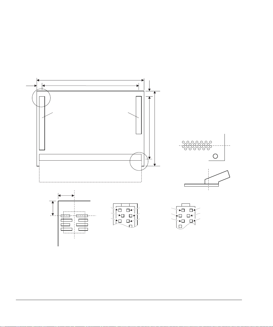
Specifications
B.3 Mechanical details
The core module is designed to be stackable on a num ber of different mothe rboards. Its
size allows it to be mounted onto a CompactPC I mo therboard while allowing the
motherboard to be installed in a card cage.
Figure B-1 shows the mechanical outline of the core module.
10.0
200-way connector
(4 col x 50 row)
Plug on top and
socket on underside
Detail A
148.0
128.0
Detail A
HDRA HDRB
130-way connector
(4 col x 30 row)
Plug on top and
socket on underside
Memory DIMM
Memory DIMM connector is 25º type
which overhangs the edge of the board
10.0
10.0
Pin numbers for 200-way plug,
viewed from above board
1
2
3
Detail B
101
102
103
10.0
100.0
81.0
Pin numbers for 200-way socket,
viewed from below board
101
102
103
Detail B
Pin numbers for 168-way
SDRAM DIMM connector
shown
Measurement datum is
line shown through pins
1
2
3
1
2
85
86
B-4
Connector footprint
Samtec TOLC series
Samtec TOLC series
© Copyright ARM Limited 1999. All rights reserved.
Figure B-1 Board outline
ARM DUI 0125A
Page 93

Index
The items in this index are listed in alphabetic order, with symbols and numerics appearing at the end. The
references given are to page numbers.
A
About this book
feedback xi
typographical co nventions ix
Access arbitration, SDRAM 3-6
Accesses
boot ROM 4-2
SSRAM 4-2
Accesses SDRAM 4-4
Alias SDRAM addresses 4-5
ARM web address ii
Assmbled Integrator syst em 2-5
B
Block diagr a m 1-4
Boot ROM, accesses 4-2
Bus bridge, system 3-11
Bus clock, processor 3-19
ARM DUI 0125A
Bus operating mo de s 3-16
C
Calculating th e CO RECLK speed 3-18
Calculating th e LCLK speed 3-19
CAS latency, setting 4-15
CE Declaration of Conf orm it y iii
Checking for valid SPD data 4-16
Clock generator 1-6, 3-17
Clock, reference 3-20
CM_CTL register 4-2
CM_CTRL register 4-11
CM_FIQ_ENCLR register 4-19
CM_FIQ_ENSET register 4-19
CM_FIQ_RSTAT register 4-19
CM_FIQ_STAT register 4-19
CM_ID Register 4-8
CM_ID register 4-5
© Copyright ARM Limited 1999. All rights reserved.
CM_IRQ_ENCLR register 4-19
CM_IRQ_ENSET register 4-19
CM_IRQ_RSTAT regist er 4-19
CM_IRQ_STAT register 4-19
CM_LOCK register 4-13
CM_OSC register 3 -18, 3-19, 4-9
CM_PROC register 4-8
CM_SDRAM 3-7
CM_SDRAM register 4-14
CM_SOFT_INTCLR register 4-19
CM_SOFT_INTSET register 4-19
CM_SPD 3-7
CM_STAT register 4-12
CONFIG LED 3-21
CONFIG link 3-21
Configuration mode 3-23
Connecting Multi-ICE 2-4
Connecting power 2-3
Index-i
Page 94

Index
Connectors
HDRA and HDRB 1-3
Multi-ICE 2-4
power 2-3
Controller
clock 1-6, 3-17
reset 1-5, 3-8
SDRAM 1-5, 3-6
SSRAM 3-3
Controllers
FIQ 4-19
IRQ 4-19
Core module control register 4-11
Core module FPGA 1-5
Core module ID 2-6
Core module registers 4-7
Core module, stack posi tio n 4-12
CORECLK 3-17, 3-18
D
Debug comms channel 4-19
Debugging modes 3-23
DIMM socket 1-3
Document confi de ntiality status ii
E
Electromagne ti c conformity i ii
Enable register, interrupt 4-20, 4-21
Ensuring safety 1-11
Exception vector mapping 4- 6
F
FCC notice iii
FIFOs 3-11
FIQ controller 4-19
Fitting SDRAM 2-2
FPGA 1-5
G
Global SDRAM 4-5
H
HDRA 3-15
HDRA and HDRB connectors 1-3
I
ID, core module 2-6
Interface
system bus 1-5
Interrupt control 4-20
Interrupt register bit assignment 4-21
Interrupt registers 4-19
Interupt status 4-20
IRQ and FIQ register bit
assignment 4-21
IRQ controller 4-19
J
JTAG 3-21
JTAG debug 1-7
JTAG scan path 3-22
JTAG signals 3-24
JTAG, connecting 2-4
L
LCLK 3-17, 3-19
Local SDRAM 4-4
Location of connectors 1-3
Lock register 4-13
M
MBDET bit 4-11
Memory
volatile 1-6
Memory map 4-2
MEMSIZE 4-15
Microprocessor core 3-2
MISC LED control 4-11
Motherboard detect 4-3
Motherboard, attachi ng t he core
module 2-5
Multi-ICE 1-7, 3-21
connecting 2-4
Multi-ICE connector 1-3
N
nLCLK 3-19
nMBDET 3-22
Normal debug mode 3-23
Notices, FCC iii
O
Operating mode, SDRAM 3-6
Oscillator register 4-9
Output divider 3- 18, 3-19
P
Power connector 1-3, 2-3
Powering an attached core module 2-6
Precautions 1-11
Preventing damage 1-11
Processor bus clock 3-19
Processor core clock 3-18
Processor register 4-8
Product feedback xi
Product status ii
Proprietary notice ii
R
Raw status register, interrupt 4-20
REFCLK 3-17, 3-20
Reference clock 3-20
Register addresses 4-7
Registers 1-6
CM_CTL 4-2
CM_CTRL 4-11
CM_FIQ_ENCLR 4-19
CM_FIQ_ENSET 4-19
CM_FIQ_RSTAT 4 -19
CM_FIQ_STAT 4-19
CM_ID 4-5, 4-8
CM_IRQ_ENCLR 4- 19
CM_IRQ_ENSET 4-19
CM_IRQ_RSTAT 4-19
CM_IRQ_STAT 4-19
CM_LOCK 4-13
CM_OSC 3-18, 3-19, 4-9
CM_PROC 4-8
CM_SDRAM 4-14
CM_SOFT_INTCLR 4-19
CM_SOFT_INTSET 4-19
CM_STAT 4-12
Related publications x
REMAP bit 4-11
Remap, effect of 4-2
Reset control bit 4-11
Reset controller 1-5, 3-8
S
SDRAM
fitting 2-2
SDRAM access arbitration 3-6
SDRAM accesses 4-4
SDRAM controller 1-5, 3-6
SDRAM global access 4-5
Index-ii
© Copyright ARM Limited 1999. All rights reserved.
ARM DUI 0125A
Page 95

SDRAM operating mo de 3-6
SDRAM repeat mapp ing 4-4
SDRAM status and control register 4-14
SDRAM, SPD memory 4-16
Serial presence detec t 3-6
Setting CAS latency 4-15
Setting SDRAM size 4-15
Setup
power connections 2-3
standalone 2-2
Software interrupt registers 4-22
Software reset 4-11
SPD memory 4-16
SPDOK bit 4-14
SSRAM accesses 4-2
SSRAM controller 3-3
Standalone core module 2-2
Status and configurat ion registers 1-6
Status register 4-12
Status register, interrupt 4-20
Supplying power 2-3
System architectu r e 1-4
System bu s
operating modes 3-16
System bus bridge 1-5, 3-11
System bus signal routing 3-15
Index
T
Typographica l conventions ix
U
Using the core module with a
motherboard 2-5
V
VCO divider 3-18, 3-19
Vector mapping 4-6
Volatile memory 1-6
W
Web site, ARM ii
ARM DUI 0125A
© Copyright ARM Limited 1999. All rights reserved.
Index-iii
Page 96

Index
Index-iv
© Copyright ARM Limited 1999. All rights reserved.
ARM DUI 0125A
 Loading...