

Page 1

ARM926EJ-S
(r0p4/r0p5)
Technical Reference Manual
Copyright © 2001-2003 ARM Limited. All rights reserved.
ARM DDI0198D
Page 2

ARM926EJ-S
Technical Reference Manual
Copyright © 2001-2003 ARM Limited. All rights reserved.
Release Information
Change history
Date Issue Change
26 September 2001 A First release
29 January 2002 B Second release
5 December 2003 C Third release. Includes r0p5 changes. Defects corrected.
26 January 2004 D Fourth release. Includes r0p4. Technically identical to previous release.
Proprietary Notice
Words and logos marked with
as otherwise stated below in this proprietary notice. Other brands and names mentioned herein may be the
trademarks of their respective owners.
Neither the whole nor any part of the information contained in, or the product described in, this document
may be adapted or reproduced in any material form except with the prior written permission of the copyright
holder.
®
or ™ are registered trademarks or trademarks owned by ARM Limited, except
The product described in this document is subject to continuous developments and improvements. All
particulars of the product and its use contained in this document are given by ARM in good faith. However,
all warranties implied or expressed, including but not limited to implied warranties of merchantability, or
fitness for purpose, are excluded.
This document is intended only to assist the reader in the use of the product. ARM Limited shall not be liable
for any loss or damage arising from the use of any information in this document, or any error or omission in
such information, or any incorrect use of the product.
Confidentiality Status
This document is Open Access. This document has no restriction on distribution.
Product Status
The information in this document is final, that is for a developed product.
Web Address
http://www.arm.com
ii Copyright © 2001-2003 ARM Limited. All rights reserved. ARM DDI0198D
Page 3

Contents
ARM926EJ-S Technical Reference Manual
Preface
About this manual ........................................................................................ xvi
Feedback ..................................................................................................... xxi
Chapter 1 Introduction
1.1 About the ARM926EJ-S processor ............................................................. 1-2
Chapter 2 Programmer’s Model
2.1 About the programmer’s model ................................................................... 2-2
2.2 Summary of ARM926EJ-S system control coprocessor (CP15) registers .. 2-3
2.3 Register descriptions .................................................................................. 2-7
Chapter 3 Memory Management Unit
3.1 About the MMU ........................................................................................... 3-2
3.2 Address translation ..................................................................................... 3-5
3.3 MMU faults and CPU aborts ..................................................................... 3-21
3.4 Domain access control .............................................................................. 3-24
3.5 Fault checking sequence .......................................................................... 3-26
3.6 External aborts .......................................................................................... 3-29
3.7 TLB structure ............................................................................................ 3-31
ARM DDI0198D Copyright © 2001-2003 ARM Limited. All rights reserved. iii
Page 4

Contents
Chapter 4 Caches and Write Buffer
4.1 About the caches and write buffer .............................................................. 4-2
4.2 Write buffer ................................................................................................. 4-4
4.3 Enabling the caches ................................................................................... 4-5
4.4 TCM and cache access priorities ............................................................... 4-8
4.5 Cache MVA and Set/Way formats .............................................................. 4-9
Chapter 5 Tightly-Coupled Memory Interface
5.1 About the tightly-coupled memory interface ............................................... 5-2
5.2 TCM interface signals ................................................................................. 5-4
5.3 TCM interface bus cycle types and timing .................................................. 5-8
5.4 TCM programmer’s model ........................................................................ 5-19
5.5 TCM interface examples ........................................................................... 5-20
5.6 TCM access penalties .............................................................................. 5-29
5.7 TCM write buffer ....................................................................................... 5-30
5.8 Using synchronous SRAM as TCM memory ............................................ 5-31
5.9 TCM clock gating ...................................................................................... 5-32
Chapter 6 Bus Interface Unit
6.1 About the bus interface unit ........................................................................ 6-2
6.2 Supported AHB transfers ............................................................................ 6-3
Chapter 7 Noncachable Instruction Fetches
7.1 About noncachable instruction fetches ....................................................... 7-2
Chapter 8 Coprocessor Interface
8.1 About the ARM926EJ-S external coprocessor interface ............................ 8-2
8.2 LDC/STC .................................................................................................... 8-4
8.3 MCR/MRC .................................................................................................. 8-6
8.4 CDP ............................................................................................................ 8-8
8.5 Privileged instructions ................................................................................. 8-9
8.6 Busy-waiting and interrupts ...................................................................... 8-10
8.7 CPBURST ................................................................................................ 8-11
8.8 CPABORT ................................................................................................ 8-12
8.9 nCPINSTRVALID ..................................................................................... 8-13
8.10 Connecting multiple external coprocessors .............................................. 8-14
Chapter 9 Instruction Memory Barrier
9.1 About the instruction memory barrier operation ......................................... 9-2
9.2 IMB operation ............................................................................................. 9-3
9.3 Example IMB sequences ............................................................................ 9-5
Chapter 10 Embedded Trace Macrocell Support
10.1 About Embedded Trace Macrocell support .............................................. 10-2
iv Copyright © 2001-2003 ARM Limited. All rights reserved. ARM DDI0198D
Page 5

Chapter 11 Debug Support
11.1 About debug support ................................................................................. 11-2
Chapter 12 Power Management
12.1 About power management ........................................................................ 12-2
Appendix A Signal Descriptions
A.1 Signal properties and requirements ............................................................ A-2
A.2 AHB related signals .................................................................................... A-3
A.3 Coprocessor interface signals ..................................................................... A-5
A.4 Debug signals ............................................................................................. A-7
A.5 JTAG signals ............................................................................................... A-9
A.6 Miscellaneous signals ............................................................................... A-10
A.7 ETM interface signals ............................................................................... A-12
A.8 TCM interface signals ............................................................................... A-14
Appendix B CP15 Test and Debug Registers
B.1 About the Test and Debug Registers .......................................................... B-2
Glossary
Contents
ARM DDI0198D Copyright © 2001-2003 ARM Limited. All rights reserved. v
Page 6

Contents
vi Copyright © 2001-2003 ARM Limited. All rights reserved. ARM DDI0198D
Page 7

List of Tables
ARM926EJ-S Technical Reference Manual
Change history .............................................................................................................. ii
Table 2-1 CP15 register summary ............................................................................................ 2-3
Table 2-2 Address types in ARM926EJ-S ................................................................................. 2-4
Table 2-3 CP15 abbreviations ................................................................................................... 2-5
Table 2-4 Reading from register c0 ........................................................................................... 2-7
Table 2-5 Register 0, ID code ................................................................................................... 2-8
Table 2-6 Ctype encoding ......................................................................................................... 2-9
Table 2-7 Cache size encoding (M=0) .................................................................................... 2-10
Table 2-8 Cache associativity encoding (M=0) ....................................................................... 2-10
Table 2-9 Line length encoding ............................................................................................... 2-11
Table 2-10 Example Cache Type Register format .................................................................... 2-11
Table 2-11 Control bit functions register c1 ............................................................................... 2-13
Table 2-12 Effects of Control Register on caches ..................................................................... 2-15
Table 2-13 Effects of Control Register on TCM interface .......................................................... 2-16
Table 2-14 Domain access control defines ............................................................................... 2-18
Table 2-15 FSR bit field descriptions ........................................................................................ 2-19
Table 2-16 FSR status field encoding ....................................................................................... 2-20
Table 2-17 Function descriptions register c7 ............................................................................ 2-21
Table 2-18 Cache operations c7 ............................................................................................... 2-22
Table 2-19 Register c8 TLB operations ..................................................................................... 2-25
Table 2-20 Cache Lockdown Register instructions ................................................................... 2-27
Table 2-21 Cache Lockdown Register L bits ............................................................................. 2-28
Table 2-22 TCM Region Register instructions .......................................................................... 2-29
ARM DDI0198D Copyright © 2001-2003 ARM Limited. All rights reserved. vii
Page 8

List of Tables
Table 2-23 TCM Region Register c9 ........................................................................................ 2-30
Table 2-24 TCM Size field encoding ......................................................................................... 2-30
Table 2-25 Programming the TLB Lockdown Register ............................................................. 2-32
Table 2-26 FCSE PID Register operations ............................................................................... 2-34
Table 2-27 Context ID register operations ................................................................................ 2-35
Table 3-1 MMU program-accessible CP15 registers ................................................................ 3-4
Table 3-2 First-level descriptor bits ........................................................................................... 3-9
Table 3-3 Interpreting first-level descriptor bits [1:0] ............................................................... 3-10
Table 3-4 Section descriptor bits ............................................................................................ 3-11
Table 3-5 Coarse page table descriptor bits ........................................................................... 3-12
Table 3-6 Fine page table descriptor bits ................................................................................ 3-13
Table 3-7 Second-level descriptor bits .................................................................................... 3-15
Table 3-8 Interpreting page table entry bits [1:0] .................................................................... 3-16
Table 3-9 Priority encoding of fault status ............................................................................... 3-22
Table 3-10 FAR values for multi-word transfers ....................................................................... 3-23
Table 3-11 Domain access control register, access control bits ............................................... 3-24
Table 3-12 Interpreting access permission (AP) bits ................................................................ 3-24
Table 4-1 CP15 c1 I and M bit settings for the ICache ............................................................. 4-5
Table 4-2 Page table C bit settings for the ICache ................................................................... 4-5
Table 4-3 CP15 c1 C and M bit settings for the DCache .......................................................... 4-6
Table 4-4 Page table C and B bit settings for the DCache ....................................................... 4-6
Table 4-5 Instruction access priorities to the TCM and cache .................................................. 4-8
Table 4-6 Data access priorities to the TCM and cache ........................................................... 4-8
Table 4-7 Values of S and NSETS ......................................................................................... 4-10
Table 5-1 Relationship between DMDMAEN, DRDMACS, and DRIDLE ................................. 5-6
Table 6-1 Supported HBURST encodings ................................................................................ 6-4
Table 6-2 IHPROT[3:0] and DHPROT[3:0] attributes ............................................................... 6-5
Table 8-1 Handshake signal encoding ...................................................................................... 8-5
Table 8-2 CPBURST encoding ............................................................................................... 8-11
Table 11-1 Scan chain 15 format .............................................................................................. 11-2
Table 11-2 Scan chain 15 mapping to CP15 registers ............................................................. 11-4
Table A-1 AHB related signals .................................................................................................. A-3
Table A-2 Coprocessor interface signals .................................................................................. A-5
Table A-3 Debug signals ........................................................................................................... A-7
Table A-4 JTAG signals ............................................................................................................ A-9
Table A-5 Miscellaneous signals ............................................................................................. A-10
Table A-6 ETM interface signals ............................................................................................. A-12
Table A-7 TCM interface signals ............................................................................................. A-14
Table B-1 Debug Override Register .......................................................................................... B-3
Table B-2 Trace Control Register bit assignments .................................................................... B-5
Table B-3 MMU test operation instructions ............................................................................... B-5
Table B-4 Encoding of the main TLB entry-select bit fields ....................................................... B-6
Table B-5 Encoding of the TLB MVA tag bit fields .................................................................... B-7
Table B-6 Encoding of the TLB entry PA and AP bit fields ....................................................... B-8
Table B-7 Main TLB mapping to MMUxWD .............................................................................. B-9
Table B-8 Encoding of the lockdown TLB entry-select bit fields ............................................. B-11
Table B-9 Cache Debug Control Register bit assignments ..................................................... B-12
viii Copyright © 2001-2003 ARM Limited. All rights reserved. ARM DDI0198D
Page 9

List of Tables
Table B-10 MMU Debug Control Register bit assignments ....................................................... B-14
Table B-11 Memory Region Remap Register instructions ......................................................... B-15
Table B-12 Encoding of the Memory Region Remap Register .................................................. B-16
Table B-13 Encoding of the remap fields ................................................................................... B-16
ARM DDI0198D Copyright © 2001-2003 ARM Limited. All rights reserved. ix
Page 10

List of Tables
x Copyright © 2001-2003 ARM Limited. All rights reserved. ARM DDI0198D
Page 11

List of Figures
ARM926EJ-S Technical Reference Manual
Key to timing diagram conventions ............................................................................ xix
Figure 1-1 ARM926EJ-S block diagram ..................................................................................... 1-3
Figure 1-2 ARM926EJ-S interface diagram (part one) ............................................................... 1-4
Figure 1-3 ARM926EJ-S interface diagram (part two) ............................................................... 1-5
Figure 2-1 CP15 MRC and MCR bit pattern ............................................................................... 2-5
Figure 2-2 Cache Type Register format ..................................................................................... 2-9
Figure 2-3 Dsize and Isize field format ....................................................................................... 2-9
Figure 2-4 TCM Status Register format .................................................................................... 2-12
Figure 2-5 Control Register format ........................................................................................... 2-13
Figure 2-6 TTBR format ............................................................................................................ 2-17
Figure 2-7 Register c3 format ................................................................................................... 2-18
Figure 2-8 FSR format .............................................................................................................. 2-19
Figure 2-9 Register c7 MVA format .......................................................................................... 2-23
Figure 2-10 Register c7 Set/Way format .................................................................................... 2-24
Figure 2-11 Register c8 MVA format .......................................................................................... 2-26
Figure 2-12 Cache Lockdown Register c9 format ...................................................................... 2-27
Figure 2-13 TCM Region Register c9 format .............................................................................. 2-30
Figure 2-14 TLB Lockdown Register format ............................................................................... 2-32
Figure 2-15 Process ID Register format ..................................................................................... 2-34
Figure 2-16 Context ID Register format ...................................................................................... 2-35
Figure 3-1 Translation Table Base Register ............................................................................... 3-6
Figure 3-2 Translating page tables ............................................................................................. 3-7
Figure 3-3 Accessing translation table first-level descriptors ...................................................... 3-8
ARM DDI0198D Copyright © 2001-2003 ARM Limited. All rights reserved. xi
Page 12

List of Figures
Figure 3-4 First-level descriptor ................................................................................................. 3-9
Figure 3-5 Section descriptor ................................................................................................... 3-10
Figure 3-6 Coarse page table descriptor .................................................................................. 3-11
Figure 3-7 Fine page table descriptor ...................................................................................... 3-12
Figure 3-8 Section translation .................................................................................................. 3-14
Figure 3-9 Second-level descriptor .......................................................................................... 3-15
Figure 3-10 Large page translation from a coarse page table ................................................... 3-17
Figure 3-11 Small page translation from a coarse page table ................................................... 3-18
Figure 3-12 Tiny page translation from a fine page table ........................................................... 3-19
Figure 3-13 Sequence for checking faults .................................................................................. 3-26
Figure 4-1 Generic virtually indexed virtually addressed cache ................................................. 4-9
Figure 4-2 ARM926EJ-S cache associativity ........................................................................... 4-10
Figure 4-3 ARM926EJ-S cache Set/Way/Word format ............................................................ 4-11
Figure 5-1 Multi-cycle data side TCM access ............................................................................ 5-8
Figure 5-2 Instruction side zero wait state accesses ................................................................. 5-9
Figure 5-3 Data side zero wait state accesses ........................................................................ 5-10
Figure 5-4 Relationship between DRDMAEN, DRDMACS, DRDMAADDR, DRADDR and DRCS ..
5-11
Figure 5-5 DMA access interaction with normal DTCM accesses ........................................... 5-12
Figure 5-6 Generating a single wait state for ITCM accesses using IRWAIT .......................... 5-13
Figure 5-7 State machine for generating a single wait state .................................................... 5-14
Figure 5-8 Loopback of SEQ to produce a single cycle wait state ........................................... 5-14
Figure 5-9 Cycle timing of loopback circuit .............................................................................. 5-15
Figure 5-10 DMA with single wait state for nonsequential accesses ......................................... 5-16
Figure 5-11 Cycle timing of circuit with DMA and single wait state for nonsequential accesses 5-17
Figure 5-12 Zero wait state RAM example ................................................................................. 5-20
Figure 5-13 Byte-banks of RAM example .................................................................................. 5-21
Figure 5-14 Optimizing for power ............................................................................................... 5-23
Figure 5-15 Optimizing for speed ............................................................................................... 5-24
Figure 5-16 TCM subsystem that uses wait states for nonsequential accesses ........................ 5-25
Figure 5-17 Cycle timing of circuit that uses wait states for non sequential accesses ............... 5-26
Figure 5-18 TCM subsystem that uses the DMA interface ........................................................ 5-27
Figure 5-19 TCM test access using BIST .................................................................................. 5-28
Figure 6-1 Multi-layer AHB system example ............................................................................. 6-8
Figure 6-2 Multi-AHB system example ...................................................................................... 6-9
Figure 6-3 AHB clock relationships .......................................................................................... 6-10
Figure 8-1 Producing a coprocessor clock ................................................................................. 8-2
Figure 8-2 Coprocessor clocking ............................................................................................... 8-2
Figure 8-3 LDC/STC cycle timing ............................................................................................... 8-4
Figure 8-4 MCR/MRC cycle timing ............................................................................................. 8-6
Figure 8-5 Interlocked MCR ....................................................................................................... 8-7
Figure 8-6 Latecanceled CDP .................................................................................................... 8-8
Figure 8-7 Privileged instructions ............................................................................................... 8-9
Figure 8-8 Busy waiting and interrupts ..................................................................................... 8-10
Figure 8-9 CPBURST and CPABORT timing ........................................................................... 8-12
Figure 8-10 Arrangement for connecting two coprocessors ...................................................... 8-14
Figure 12-1 Deassertion of STANDBYWFI after an IRQ interrupt ............................................. 12-2
xii Copyright © 2001-2003 ARM Limited. All rights reserved. ARM DDI0198D
Page 13

List of Figures
Figure 12-2 Logic for stopping ARM926EJ-S clock during wait for interrupt .............................. 12-3
Figure B-1 CP15 MRC and MCR bit pattern ............................................................................... B-2
Figure B-2 Rd format for selecting main TLB entry ..................................................................... B-6
Figure B-3 Rd format for accessing MVA tag of main or lockdown TLB entry ............................ B-7
Figure B-4 Rd format for accessing PA and AP data of main or lockdown TLB entry ................ B-8
Figure B-5 Write to the data RAM ............................................................................................. B-10
Figure B-6 Rd format for selecting lockdown TLB entry ........................................................... B-11
Figure B-7 Cache Debug Control Register format .................................................................... B-12
Figure B-8 MMU Debug Control Register format ...................................................................... B-14
Figure B-9 Memory Region Remap Register format ................................................................. B-15
Figure B-10 Memory region attribute resolution .......................................................................... B-17
ARM DDI0198D Copyright © 2001-2003 ARM Limited. All rights reserved. xiii
Page 14

List of Figures
xiv Copyright © 2001-2003 ARM Limited. All rights reserved. ARM DDI0198D
Page 15

Preface
This preface introduces the ARM926EJ-S Revision r0p4/r0p5 Technical Reference
Manual (TRM). It contains the following sections:
• About this manual on page xvi
• Feedback on page xxi.
ARM DDI0198D Copyright © 2001-2003 ARM Limited. All rights reserved. xv
Page 16

Preface
About this manual
This is the Technical Reference Manual for the ARM926EJ-S processor.
Product revision status
The rnpn identifier indicates the revision status of the product described in this manual,
where:
rn Identifies the major revision of the product.
pn Identifies the minor revision or modification status of the product.
Intended audience
This document has been written for experienced hardware and software engineers who
have previous experience of ARM products, and who wish to use an ARM926EJ-S
processor in their system design.
Using this manual
This document is organized into the following chapters:
Chapter 1 Introduction
Read this chapter for an overview of the ARM926EJ-S processor.
Chapter 2 Programmer’s Model
Read this chapter for details of the programmer’s model and
ARM926EJ-S registers.
Chapter 3 Memory Management Unit
Read this chapter for details of the Memory Management Unit (MMU)
and address translation process and how to use the CP15 register to
enable and disable the MMU.
Chapter 4 Caches and Write Buffer
Read this chapter for a description of the instruction cache, the data
cache, the write buffer, and the physical address tag RAM.
Chapter 5 Tightly-Coupled Memory Interface
Read this chapter for a description of the Tightly-Coupled Memory
(TCM) interface and how to use the CP15 region register to enable and
disable the caches. It includes examples on how various RAM types can
be connected.
xvi Copyright © 2001-2003 ARM Limited. All rights reserved. ARM DDI0198D
Page 17

Chapter 6 Bus Interface Unit
Read this chapter for a description of the Bus Interface Unit (BIU)
interface to AMBA.
Chapter 7 Noncachable Instruction Fetches
Read this chapter for a description of how speculative noncachable
instruction fetches are used in the ARM926EJ-S processor to improve
performance.
Chapter 8 Coprocessor Interface
Read this chapter for a description of the coprocessor interface. The
chapter includes timing diagrams for coprocessor operations.
Chapter 9 Instruction Memory Barrier
Read this chapter for the Instruction Memory Barrier (IMB) description
and how IMB operations are used to ensure consistency between data and
instruction streams processed by the ARM926EJ-S processor.
Chapter 10 Embedded Trace Macrocell Support
Read this chapter to understand how Embedded Trace Macrocell (ETM)
is supported in the ARM926EJ-S processor.
Preface
Chapter 11 Debug Support
Read this chapter for a description of the debug interface and
EmbeddedICE-RT.
Chapter 12 Power Management
Read this chapter for a description of the power management facilities
provided by the ARM926EJ-S processor.
Appendix A Signal Descriptions
This appendix lists the ARM926EJ-S processor signals in functional
groups.
Appendix B CP15 Test and Debug Registers
Read this appendix for detailed information on the registers used for test
and debug.
ARM DDI0198D Copyright © 2001-2003 ARM Limited. All rights reserved. xvii
Page 18

Preface
Conventions
This section describes the conventions that this manual uses:
• Typographical
• Timing diagrams
• Signal naming on page xix
• Numbering on page xx.
Typographical
This manual uses the following typographical conventions:
italic Highlights important notes, introduces special terminology,
denotes internal cross-references, and citations.
bold Highlights interface elements, such as menu names. Denotes
ARM processor signal names. Also used for terms in descriptive
lists, where appropriate.
monospace
Denotes text that you can enter at the keyboard, such as
commands, file and program names, and source code.
monospace
Denotes a permitted abbreviation for a command or option. You
can enter the underlined text instead of the full command or option
name.
monospace italic
Denotes arguments to monospace text where the argument is to be
replaced by a specific value.
monospace bold
denotes language keywords when used outside example code.
< and > Angle brackets enclose replaceable terms for assembler syntax
where they appear in code or code fragments. They appear in
normal font in running text. For example:
•
MRC p15, 0 <Rd>, <CRn>, <CRm>, <Opcode_2>
• The Opcode_2 value selects which register is accessed.
Timing diagrams
This manual contains one or more timing diagrams. The figure named Key to timing
diagram conventions on page xix on page xix explains the components used in these
diagrams. When variations occur they have clear labels. You must not assume any
timing information that is not explicit in the diagrams.
xviii Copyright © 2001-2003 ARM Limited. All rights reserved. ARM DDI0198D
Page 19

Preface
Clock
HIGH to LOW
Transient
HIGH/LOW to HIGH
Bus stable
Bus to high impedance
Bus change
High impedance to stable bus
Key to timing diagram conventions
Signal naming
The level of an asserted signal depends on whether the signal is active-HIGH or
active-LOW. Asserted means HIGH for active-HIGH signals and LOW for active-LOW
signals:
Prefix H Denotes Advanced High-performance Bus (AHB) signals.
Prefix n Denotes active-LOW signals except in the case of AHB or Advanced
Peripheral Bus APB reset signals. These are named HRESETn and
PRESETn respectively.
Prefix DH Denotes data side AHB signals.
Prefix IH Denotes instruction side AHB signals.
Prefix DR Denotes data side TCM interface signals.
Prefix IR Denotes instruction side TCM interface signals.
Prefix ETM Denotes ETM interface signals.
Prefix DBG Denotes debug/JTAG signals.
Prefix CP Denotes coprocessor interface signals.
ARM DDI0198D Copyright © 2001-2003 ARM Limited. All rights reserved. xix
Page 20

Preface
Further reading
Numbering
<size in bits>’<base><number>
This is a Verilog method of abbreviating constant numbers. For example:
•‘h7B4 is an unsized hexadecimal value.
•‘o7654 is an unsized octal value.
• 8’d9 is an eight-bit wide decimal value of 9.
0x3F
• 8’h3F is an eight-bit wide hexadecimal value of
. This is
equivalent to b00111111.
• 8’b1111 is an eight-bit wide binary value of b00001111.
This section lists publications by ARM Limited, and by third parties.
ARM Limited periodically provides updates and corrections to its documentation. See
http://www.arm.com
for current errata sheets, addenda, and the ARM Limited
Frequently Asked Questions list.
ARM publications
This manual contains information that is specific to the ARM926EJ-S processor. Refer
to the following documents for other relevant information:
• ARM Architecture Reference Manual (ARM DDI 0100)
• ARM AMBA Specification (Rev 2.0) (ARM IHI 0001)
• ARM926EJ-S Implementation Guide (ARM DII 0015)
• ARM926EJ-S Test Chip Implementation Guide (ARM DXI 0131)
• ARM9EJ-S Technical Reference Manual (ARM DDI 0222)
• Multi-layer AHB Overview (ARM DVI 0045)
• ETM9 Technical Reference Manual (ARM DDI 0157).
xx Copyright © 2001-2003 ARM Limited. All rights reserved. ARM DDI0198D
Page 21

Feedback
ARM Limited welcomes feedback on the ARM926EJ-S processor and its
documentation.
Feedback on the product
If you have any comments or suggestions about this product, contact your supplier
giving:
• the product name
• a concise explanation of your comments.
Feedback on this manual
Preface
If you have any comments on this manual, send email to
errata@arm.com
giving:
• the title
• the number
• the relevant page number(s) to which your comments apply
• a concise explanation of your comments.
ARM Limited also welcomes general suggestions for additions and improvements.
ARM DDI0198D Copyright © 2001-2003 ARM Limited. All rights reserved. xxi
Page 22

Preface
xxii Copyright © 2001-2003 ARM Limited. All rights reserved. ARM DDI0198D
Page 23

Chapter 1
Introduction
This chapter introduces the ARM926EJ-S processor and its features. It contains the
following section:
• About the ARM926EJ-S processor on page 1-2.
ARM DDI0198D Copyright © 2001-2003 ARM Limited. All rights reserved. 1-1
Page 24

Introduction
1.1 About the ARM926EJ-S processor
The ARM926EJ-S processor is a member of the ARM9 family of general-purpose
microprocessors. The ARM926EJ-S processor is targeted at multi-tasking applications
where full memory management, high performance, low die size, and low power are all
important.
The ARM926EJ-S processor supports the 32-bit ARM and 16-bit Thumb instruction
sets, enabling the user to trade off between high performance and high code density. The
ARM926EJ-S processor includes features for efficient execution of Java byte codes,
providing Java performance similar to JIT, but without the associated code overhead.
The ARM926EJ-S processor supports the ARM debug architecture and includes logic
to assist in both hardware and software debug. The ARM926EJ-S processor has a
Harvard cached architecture and provides a complete high-performance processor
subsystem, including:
• an ARM9EJ-S integer core
• a Memory Management Unit (MMU)
• separate instruction and data AMBA AHB bus interfaces
• separate instruction and data TCM interfaces.
The ARM926EJ-S processor provides support for external coprocessors enabling
floating-point or other application-specific hardware acceleration to be added. The
ARM926EJ-S processor implements ARM architecture version 5TEJ.
The ARM926EJ-S processor is a synthesizable macrocell. This means that you can
optimize the macrocell for a particular target library, and that you can configure the
memory system to suit your target application. You can individually configure the cache
sizes to be any power of two between 4KB and 128KB.
The tightly-coupled instruction and data memories are instantiated externally to the
ARM926EJ-S macrocell, providing you with the flexibility of optimizing the memory
subsystem for performance, power, and particular RAM type. The TCM interfaces
enable nonzero wait state memory to be attached, as well as providing a mechanism for
supporting DMA.
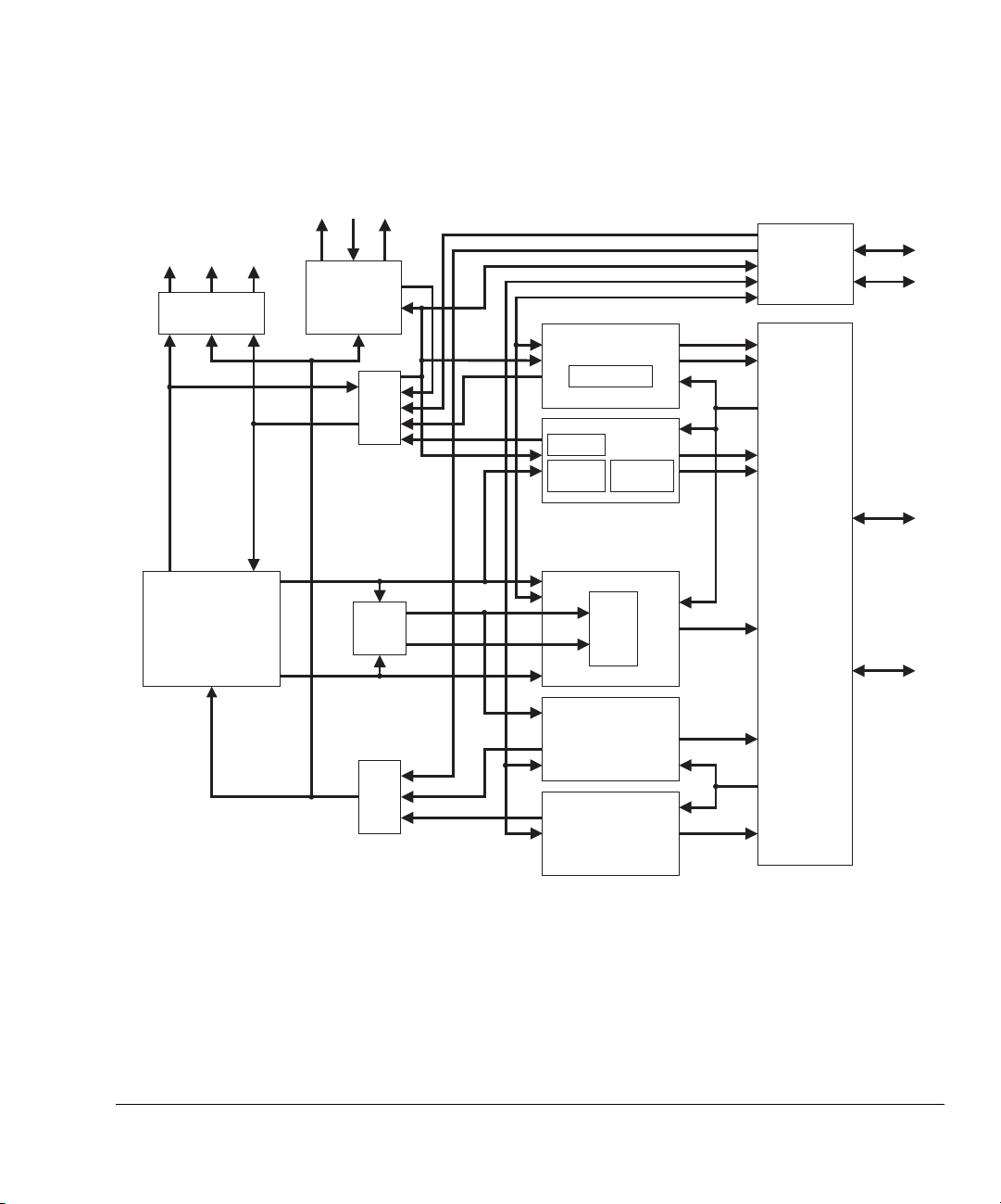
Figure 1-1 on page 1-3 shows the main blocks in the ARM926EJ-S processor.
1-2 Copyright © 2001-2003 ARM Limited. All rights reserved. ARM DDI0198D
Page 25
ETM
interface
External
coprocessor
interface
CPDINCPDOUT CPINSTR
Coprocessor
interface
DEXT
DRDATA
IRDATA
DRWDATA
TCM
interface
Introduction
ITCM
DTCM
WDATA RDATA
DA
ARM9EJ-S FCSE
INSTR
IA
DROUTE
IROUTE
DMVA
IMVA
Write buffer
DCACHE
Cache
PA
TAGRAM
ICACHE
write buffer
MMU
TLB
IEXT
Writeback
interfac e
Bus
interface
unit
Instruction
interfac e
Data
AHB
AHB
AHB
AHB
Figure 1-1 ARM926EJ-S block diagram
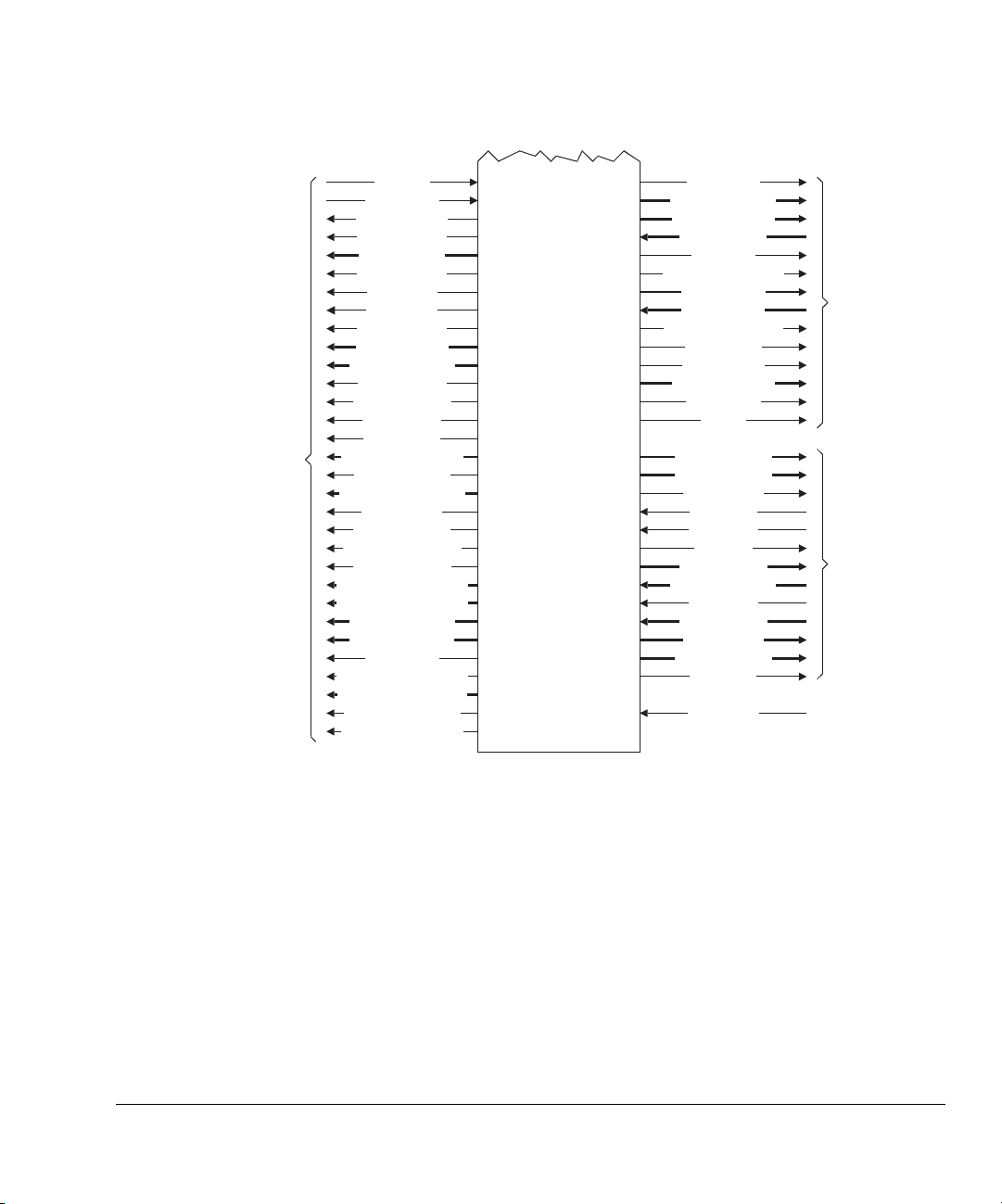
Figure 1-2 on page 1-4 and Figure 1-3 on page 1-5 show the ARM926EJ-S interfaces.
ARM DDI0198D Copyright © 2001-2003 ARM Limited. All rights reserved. 1-3
Page 26
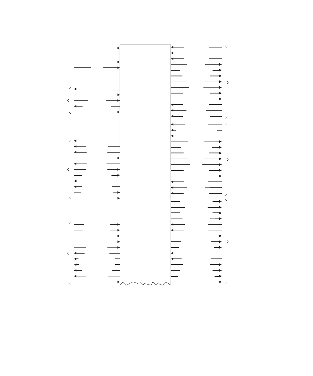
Introduction
Clock
Interrupts
Miscellaneous
configuration
JTAG debug
Debug
CLK
nFIQ
nIRQ
STANDBYWFI
BIGENDINIT
VINITHI
CFGBIGEND
TAPID[31:0]
COMMRX
COMMTX
DBGACK
DBGEN
DBGRQI
EDBGRQ
DBGEXT[1:0]
DBGINSTREXEC
DBGRNG[1:0]
DBGIEBRKPT
DBGDEWPT
DBGnTRST
DBGTCKEN
DBGTDI
DBGTMS
DBGTDO
DBGIR[3:0]
DBGSCREG[4:0]
DBGTAPSM[3:0]
DBGnTDOEN
DBGSDIN
DBGSDOUT
ARM926EJ-S
DRDMAEN
DRDMAADDR[17:0]
DRDMACS
DRnRW
DRADDR[17:0]
DRWR[31:0]
DRIDLE
DRCS
DRWBL[3:0]
DRSEQ
DRRD[31:0]
DRWAIT
DRSIZE[3:0]
IRDMAEN
IRDMAADDR[17:0]
IRDMACS
IRnRW
IRADDR[17:0]
IRWR[31:0]
IRIDLE
IRCS
IRWBL[3:0]
IRSEQ
IRRD[31:0]
IRWAIT
IRSIZE[3:0]
DHADDR[31:0]
DHBL[3:0]
DHBURST[2:0]
DHBUSREQ
DHCLKEN
DHGRANT
DHLOCK
DHPROT[3:0]
DHRDATA[31:0]
DHREADY
DHRESP[1:0]
DHSIZE[2:0]
DHTRANS[1:0]
DHWDATA[31:0]
DHWRITE
Data
memory
interface
Instruction
memory interface
Data
AHB
Figure 1-2 ARM926EJ-S interface diagram (part one)
1-4 Copyright © 2001-2003 ARM Limited. All rights reserved. ARM DDI0198D
Page 27
Introduction
ETM interface
ETMEN
FIFOFULL
ETMBIGEND
ETMHIVECS
ETMIA[31:0]
ETMInNREQ
ETMISEQ
ETMITBIT
ETMIABORT
ETMDA[31:0]
ETMDMAS[1:0]
ETMDMORE
ETMDnMREQ
ETMDnRW
ETMDSEQ
ETMRDATA[31:0]
ETMDABORT
ETMWDATA[31:0]
ETMnWAIT
ETMDBGACK
ETMINSTREXEC
ETMRNGOUT
ETMID31TO25[6:0]
ETMID15TO11[4:0]
ETMCHSD[1:0]
ETMCHSE[1:0]
ETMPASS
ETMLATECANCEL
ETMPROCID[31:0]
ETMPROCIDWR
ETMINSTRVALID
ARM926EJ-S
CPCLKEN
CPINSTR[31:0]
CPDOUT[31:0]
CPDIN[31:0]
CPPASS
CPLATECANCEL
CHSDE[1:0]
CHSEX[1:0]
nCPINSTRVALID
nCPMREQ
nCPTRANS
CPBURST[3:0]
CPABORT
CPEN
IHADDR[31:0]
IHBURST[2:0]
IHBUSREQ
IHCLKEN
IHGRANT
IHLOCK
IHPROT[3:0]
IHRDATA[31:0]
IHREADY
IHRESP[1:0]
IHSIZE[2:0]
IHTRANS[1:0]
IHWRITE
HRESETn
Coprocessor
Instruction
AHB
AHB
Figure 1-3 ARM926EJ-S interface diagram (part two)
ARM DDI0198D Copyright © 2001-2003 ARM Limited. All rights reserved. 1-5
Page 28

Introduction
1-6 Copyright © 2001-2003 ARM Limited. All rights reserved. ARM DDI0198D
Page 29

Chapter 2
Programmer’s Model
This chapter describes the ARM926EJ-S registers in CP15, the system control
coprocessor, and provides information for programming the microprocessor. It contains
the following sections:
• About the programmer’s model on page 2-2
• Summary of ARM926EJ-S system control coprocessor (CP15) registers on
page 2-3
• Register descriptions on page 2-7.
ARM DDI0198D Copyright © 2001-2003 ARM Limited. All rights reserved. 2-1
Page 30

Programmer’s Model
2.1 About the programmer’s model
The system control coprocessor (CP15) is used to configure and control the
ARM926EJ-S processor. The caches, Tightly-Coupled Memories (TCMs), Memory
Management Unit (MMU), and most other system options are controlled using CP15
registers. You can only access CP15 registers with MRC and MCR instructions in a
privileged mode. CDP, LDC, STC, MCRR, and MRRC instructions, and unprivileged
MRC or MCR instructions to CP15 cause the Undefined instruction exception to be
taken.
2-2 Copyright © 2001-2003 ARM Limited. All rights reserved. ARM DDI0198D
Page 31

Programmer’s Model
2.2 Summary of ARM926EJ-S system control coprocessor (CP15) registers
CP15 defines 16 registers. Table 2-1 shows the read and write functions of the registers.
Table 2-1 CP15 register summary
Register Reads Writes
0
0
0
a
ID code
Cache type
TCM status
Unpredictable
a
a
Unpredictable
Unpredictable
1 Control Control
2 Translation table base Translation table base
3 Domain access control Domain access control
4 Reserved Reserved
5
5
Data fault status
Instruction fault status
a
a
Data fault status
Instruction fault status
a
6 Fault address Fault address
7 Cache operations Cache operations
8 Unpredictable TLB operations
9
Cache lockdown
b
Cache lockdown
9 TCM region TCM region
10 TLB lockdown TLB lockdown
a
11 and 12 Reserved Reserved
13
13
FCSE PID
Context ID
a
a
FCSE PID
Context ID
a
a
14 Reserved Reserved
15 Test configuration Test configuration
a. Register locations 0, 5, and 13 each provide access to more than one register. The register
accessed depends on the value of the
b. Register location 9 provides access to more than one register. The register accessed depends
on the value of the
ARM DDI0198D Copyright © 2001-2003 ARM Limited. All rights reserved. 2-3
CRm
field. See the register descriptions for details.
Opcode_2
field.
Page 32

Programmer’s Model
All CP15 register bits that are defined and contain state are set to 0 by Reset except:
• The V bit is set to 0 at reset if the VINITHI signal is LOW, or 1 if the VINITHI
signal is HIGH.
• The B bit is set to 0 at reset if the BIGENDINIT signal is LOW, or 1 if the
BIGENDINIT signal is HIGH.
• The instruction TCM is enabled at reset if the INITRAM pin is HIGH. This
enables booting from the instruction TCM and sets the ITCM bit in the ITCM
region register to 1.
2.2.1 Addresses in an ARM926EJ-S system
Three distinct types of address exist in an ARM926EJ-S system. Table 2-2 shows the
address types in ARM926EJ-S processor.
Domain ARM9EJ-S Caches and MMU TCM and AMBA bus
Address type Virtual Address (VA) Modified Virtual Address (MVA) Physical Address (PA)
Table 2-2 Address types in ARM926EJ-S
This is an example of the address manipulation that occurs when the ARM9EJ-S core
requests an instruction:
1. The VA of the instruction is issued by the ARM9EJ-S core.
2. The VA is translated using the FCSE PID value to the MVA. The Instruction
Cache (ICache) and Memory Management Unit (MMU) detect the MVA (see
Process ID Register c13 on page 2-33).
3. If the protection check carried out by the MMU on the MVA does not abort and
the MVA tag is in the ICache, the instruction data is returned to the ARM9EJ-S
core.
4. If the protection check carried out by the MMU on the MVA does not abort, and
the cache misses (the MVA tag is not in the cache), then the MMU translates the
MVA to produce the PA. This address is given to the AMBA bus interface to
perform an external access.
2.2.2 Accessing CP15 registers
You can only access CP15 registers with MRC and MCR instructions in a privileged
mode. The instruction bit pattern of the MCR and MRC instructions is shown in
Figure 2-1 on page 2-5.
2-4 Copyright © 2001-2003 ARM Limited. All rights reserved. ARM DDI0198D
Page 33

Programmer’s Model
31 28 27 26 25 24 23 21 20 19 16 15 12 11 10 9 8 7 5 4 3 0
Cond
1 1 1 0
Opcode
_1
L CRn Rd 1 1 1 1
Opcode
_2
1 CRm
Figure 2-1 CP15 MRC and MCR bit pattern
The mnemonics for these instructions are:
MCR{cond} p15,<Opcode_1>,<Rd>,<CRn>,<CRm>,<Opcode_2>
MRC{cond} p15,<Opcode_1>,<Rd>,<CRn>,<CRm>,<Opcode_2>
Attempting to read from a write-only register, or writing to a read-only register causes
Unpredictable results. In all instructions that access CP15:
• The Opcode_1 field Should Be Zero except when the values specified are used to
select the desired operations. Using other values results in Unpredictable
behavior.
• The Opcode_2 and CRm fields Should Be Zero except when the values specified
are used to select the desired behavior. Using other values results in Unpredictable
behavior.
Table 2-3 shows the terms and abbreviations used in this chapter.
Table 2-3 CP15 abbreviations
Term Abbreviation Description
Unpredictable UNP For reads: The data returned when reading from
this location is unpredictable. It can have any
value.
For writes: Writing to this location causes
unpredictable behavior, or an unpredictable
change in device configuration.
Undefined UND An instruction that accesses CP15 in the manner
indicated takes the Undefined instruction
exception.
Should Be Zero SBZ When writing to this location, all bits of this field
Should Be Zero.
ARM DDI0198D Copyright © 2001-2003 ARM Limited. All rights reserved. 2-5
Page 34

Programmer’s Model
Table 2-3 CP15 abbreviations (continued)
Term Abbreviation Description
Should Be One SBO When writing to this location, all bits in this field
Should Be One.
Should Be Zero or
Preserved
SBZP When writing to this location, all bits of this field
Should Be Zero or preserved by writing the same
value that has been previously read from the same
field.
In all cases, reading from, or writing any data values to any CP15 registers, including
those fields specified as Unpredictable, Should Be One, or Should Be Zero does not
cause any physical damage to the chip.
2-6 Copyright © 2001-2003 ARM Limited. All rights reserved. ARM DDI0198D
Page 35

2.3 Register descriptions
The following registers are described in this section:
• ID Code, Cache Type, and TCM Status Registers, c0
• Control Register c1 on page 2-12
• Translation Table Base Register c2 on page 2-17
• Domain Access Control Register c3 on page 2-17
• Register c4 on page 2-18
• Fault Status Registers c5 on page 2-18
• Fault Address Register c6 on page 2-20
• Cache Operations Register c7 on page 2-20
• TLB Operations Register c8 on page 2-24
• Cache Lockdown and TCM Region Registers c9 on page 2-26
• TLB Lockdown Register c10 on page 2-32
• Register c11 and c12 on page 2-33
• Process ID Register c13 on page 2-33
• Register c14 on page 2-35
• Test and Debug Register c15 on page 2-36.
Programmer’s Model
2.3.1 ID Code, Cache Type, and TCM Status Registers, c0
Register c0 accesses the ID Register, Cache Type Register, and TCM Status Registers.
Reading from this register returns the device ID, the cache type, or the TCM status
depending on the value of Opcode_2 used:
Opcode_2 = 0 ID value.
Opcode_2 = 1 instruction and data cache type.
Opcode_2 = 2 TCM status.
The CRm field Should Be Zero when reading from these registers. Table 2-4 shows the
instructions you can use to read register c0.
Table 2-4 Reading from register c0
Function Instruction
Read ID code
Read cache type
Read TCM status
MRC p15,0,<Rd>,c0,c0,{0, 3-7}
MRC p15,0,<Rd>,c0,c0,1
MRC p15,0,<Rd>,c0,c0,2
Writing to register c0 is Unpredictable.
ARM DDI0198D Copyright © 2001-2003 ARM Limited. All rights reserved. 2-7
Page 36

Programmer’s Model
ID Code Register c0
This is a read-only register that returns the 32-bit device ID code.
You can access the ID Code Register by reading CP15 register c0 with the Opcode_2
field set to any value other than 1 or 2. For example:
MRC p15, 0, <Rd>, c0, c0, {0, 3-7} ;returns ID
The contents of the ID Code Register are shown in Table 2-5.
Table 2-5 Register 0, ID code
Register bits Function Value
[31:24] ASCII code of implementer trademark
[23:20] Variant
[19:16] Architecture (ARMv5TEJ)
[15:4] Part number
[3:0] Revision
a. The revision value can be in the range 0x0 to 0x5, depending on the
layout revision you are using..
0x41
0x0
0x6
0x926
0x05
a
Cache Type Register c0
This is a read-only register that contains information about the size and architecture of
the Instruction Cache (ICache) and Data Cache (DCache) enabling operating systems
to establish how to perform such operations as cache cleaning and lockdown.
You can access the cache type register by reading CP15 register c0 with the Opcode_2
field set to 1. For example:
MRC p15, 0, <Rd>, c0, c0, 1; returns cache details
The format of the Cache Type Register is shown in Figure 2-2 on page 2-9.
2-8 Copyright © 2001-2003 ARM Limited. All rights reserved. ARM DDI0198D
Page 37

Programmer’s Model
31 30 29 28 25 24 23 12 11 0
0
0 0 Ctype S Dsize Isize
Figure 2-2 Cache Type Register format
Ctype The Ctype field determines the cache type. See Table 2-6.
S bit Specifies if the cache is a unified cache (S=0), or separate ICache and
DCache (S=1). If S=0, the Isize and Dsize fields both describe the unified
cache and must be identical. In the ARM926EJ-S processor, this bit is set
to a 1 to denote separate caches.
Dsize Specifies the size, line length, and associativity of the DCache, or of the
unified cache if the S bit is 0.
Isize Specifies the size, length, and associativity of the ICache, or of the
unified cache if the S bit is 0.
The Ctype field specifies if the cache supports lockdown or not, and how it is cleaned.
The encoding is shown in Table 2-6. All unused values are reserved.
Table 2-6 Ctype encoding
Value Method Cache cleaning Cache lockdown
b1110 Write-back Register 7 operations
a. See Cache Lockdown Register c9 on page 2-26 for more details on
Format C for cache lockdown.
Format C
a
The Dsize and Isize fields in the Cache Type Register have the same format. This is
shown in Figure 2-3.
11 10 9 6 5 3 2 1 0
0 0 Size Assoc M Len
Figure 2-3 Dsize and Isize field format
Size The Size field determines the cache size in conjunction with the M bit.
ARM DDI0198D Copyright © 2001-2003 ARM Limited. All rights reserved. 2-9
Page 38

Programmer’s Model
Assoc The Assoc field determines the cache associativity in conjunction with
the M bit.
M bit The multiplier bit determines the cache size and cache associativity
values in conjunction with the Size and Assoc fields. If the cache is
present, M must be set to 0. If the cache is absent, M must be set to 1. For
the ARM926EJ-S processor, M is always set to 0.
Len The Len field determines the line length of the cache.
The size of the cache is determined by the Size field and the M bit. The M bit is 0 for
the DCache and ICache. The Size field is bits [21:18] for the DCache and bits [9:6] for
the ICache. The minimum size of each cache is 4KB, and the maximum size is 128KB.
Table 2-7 shows the cache size encoding.
Table 2-7 Cache size encoding (M=0)
Size field Cache size
b0011 4KB
b0100 8KB
b0101 16KB
b0110 32KB
b0111 64KB
b1000 128KB
The associativity of the cache is determined by the Assoc field and the M bit. The M bit
is 0 for the DCache and ICache. The Assoc field is bits [17:15] for the DCache and bits
[5:3] for the ICache. Table 2-8 shows the cache associativity encoding.
Table 2-8 Cache associativity encoding (M=0)
Assoc field Associativity
b010 4-way
Other values Reserved
2-10 Copyright © 2001-2003 ARM Limited. All rights reserved. ARM DDI0198D
Page 39

Programmer’s Model
The line length of the cache is determined by the Len field. The Len field is bits [13:12]
for the DCache and bits [1:0] for the ICache. Table 2-9 shows the line length encoding.
Table 2-9 Line length encoding
Len field Cache line length
b10 8 words (32 bytes)
Other values Reserved
The cache type register values for an ARM926EJ-S processor with the following
configuration are shown in Table 2-10:
• separate instruction and data caches
• DCache size = 8KB, ICache size = 16KB
• associativity = 4-way
• line length = eight words
• caches use write-back, register 7 for cache cleaning, and Format C for cache
lockdown.
See Cache Lockdown Register c9 on page 2-26 for more details on Format C for cache
lockdown.
Table 2-10 Example Cache Type Register format
Function Register bits Value
Reserved [31:29] b000
Ctype [28:25] b1110
S [24] b1 = Harvard cache
Dsize Reserved [23:22] b00
Size [21:18] b0100 = 8KB
Assoc [17:15] b010 = 4-way
M[14] b0
Len [13:12] b10 = 8 words per line (32 bytes)
ARM DDI0198D Copyright © 2001-2003 ARM Limited. All rights reserved. 2-11
Page 40

Programmer’s Model
Table 2-10 Example Cache Type Register format (continued)
Function Register bits Value
Isize Reserved [11:10] b00
Size [9:6] b0101 = 16KB
Assoc [5:3] b010 = 4-way
M[2] b0
Len [1:0] b10 = 8 words per line (32 bytes)
TCM Status Register c0
This is a read-only register that enables operating systems to establish if TCM memories
are present. See also TCM Region Register c9 on page 2-29.
You can access the TCM Status Register by reading CP15 register c0 with the Opcode_2
field set to 2. For example:
MRC p15,0,<Rd>,c0,c0,2 ;returns TCM details
The format of the TCM Status Register is shown in Figure 2-4.
31 17 16 15 1 0
SBZ/UNP
DTCM
present
Figure 2-4 TCM Status Register format
SBZ/UNP
ITCM
present
2.3.2 Control Register c1
Register c1 is the Control Register for the ARM926EJ-S processor. This register
specifies the configuration used to enable and disable the caches and MMU. It is
recommended that you access this register using a read-modify-write sequence.
For both reading and writing, the CRm and Opcode_2 fields Should Be Zero. To read
and write this register, use the instructions:
MRC p15, 0, <Rd>, c1, c0, 0 ; read control register
2-12 Copyright © 2001-2003 ARM Limited. All rights reserved. ARM DDI0198D
Page 41

Programmer’s Model
MCR p15, 0, <Rd>, c1, c0, 0 ; write control register
All defined control bits are set to zero on reset except the V bit and the B bit. The V bit
is set to zero at reset if the VINITHI signal is LOW, or one if the VINITHI signal is
HIGH. The B bit is set to zero at reset if the BIGENDINIT signal is LOW, or one if the
BIGENDINIT signal is HIGH.
Figure 2-5 shows the format of the Control Register.
31 19 18 17 16 15 14 13 12 11 10 9 8 7 6 3 2 1 0
S
S
S
L4R
B
B
B
Z
O
O
V I SBZ R S B SBO C A
R
Figure 2-5 Control Register format
Table 2-11 describes the functions of the Control Register bits.
Table 2-11 Control bit functions register c1
Bit Name Function
MSBZ
[31:19] - Reserved.
When read returns an Unpredictable value.
When written Should Be Zero, or a value read from bits [31:19] on the
same processor.
Using a read-modify-write sequence when modifying this register
provides the greatest future compatibility.
[18] - Reserved, SBO. Read = 1, write = 1.
[17] - Reserved, SBZ. Read = 0, write = 0.
[16] - Reserved, SBO. Read = 1, write = 1.
[15] L4 bit Determines if the T bit is set when load instructions change the PC:
0 = loads to PC set the T bit
1 = loads to PC do not set T bit (ARMv4 behavior).
For more details see the ARM Architecture Reference Manual.
[14] RR bit Replacement strategy for ICache and DCache:
0 = Random replacement
1 = Round-robin replacement.
ARM DDI0198D Copyright © 2001-2003 ARM Limited. All rights reserved. 2-13
Page 42

Programmer’s Model
Table 2-11 Control bit functions register c1 (continued)
Bit Name Function
[13] V bit Location of exception vectors:
0 = Normal exception vectors selected, address range =
0x0000 001C
1 = High exception vectors selected, address range =
0xFFFF 001C
.
Set to the value of VINITHI on reset.
[12] I bit ICache enable/disable:
0 = ICache disabled
1 = ICache enabled.
[11:10] - SBZ.
[9] R bit ROM protection.
This bit modifies the ROM protection system. See Domain access
control on page 3-24.
[8] S bit System protection.
This bit modifies the MMU protection system. See Domain access
control on page 3-24.
0x0000 0000
0xFFFF 0000
to
to
[7] B bit Endianness: 0 = Little-endian operation 1 = Big-endian operation. Set to
the value of BIGENDINIT on reset.
[6:3] - Reserved. SBO.
[2] C bit DCache enable/disable:
0 = Cache disabled
1 = Cache enabled.
[1] A bit Alignment fault enable/disable:
0 = Data address alignment fault checking disabled
1 = Data address alignment fault checking enabled.
[0] M bit MMU enable/disable:
0 = disabled
1 = enabled.
Effects of Control Register on caches
The bits of the Control Register that directly affect the ICache and DCache behavior are:
• the M bit
• the C bit
• the I bit
2-14 Copyright © 2001-2003 ARM Limited. All rights reserved. ARM DDI0198D
Page 43

• the RR bit.
Assuming that TCM regions are disabled, the caches behave as shown in Table 2-12.
Cache MMU Behavior
Programmer’s Model
Table 2-12 Effects of Control Register on caches
ICache disabled Enabled or
disabled
ICache enabled Disabled All instruction fetches are cachable, with no protection checks. All addresses are flat
ICache enabled Enabled Instruction fetches are cachable or noncachable, and protection checks are performed.
DCache disabled Enabled or
disabled
DCache enabled Disabled All data accesses are noncachable nonbufferable. All addresses are flat mapped. That
DCache enabled Enabled All data accesses are cachable or noncachable, and protection checks are performed.
All instruction fetches are from external memory (AHB).
mapped. That is VA = MVA = PA.
All addresses are remapped from VA to PA, depending on the MMU page table entry.
That is, VA translated to MVA, MVA remapped to PA.
All data accesses are to external memory (AHB).
is VA = MVA = PA.
All addresses are remapped from VA to PA, depending on the MMU page table entry.
That is, VA translated to MVA, MVA remapped to PA.
If either the DCache or the ICache is disabled, then the contents of that cache are not
accessed. If the cache is subsequently re-enabled, the contents will not have changed.
To guarantee that memory coherency is maintained, the DCache must be cleaned of
dirty data before it is disabled.
ARM DDI0198D Copyright © 2001-2003 ARM Limited. All rights reserved. 2-15
Page 44

Programmer’s Model
Effects of the Control Register on TCM interface
The M bit of the Control Register, when combined with the En bit in the respective TCM
region register c9, directly affects the TCM interface behavior, as shown in Table 2-13.
TCM MMU Cache Behavior
Table 2-13 Effects of Control Register on TCM interface
Instruction
TCM disabled
Instruction
TCM enabled
Instruction
TCM enabled
Instruction
TCM enabled
Data TCM
disabled
Data TCM
enabled
Data TCM
enabled
Disabled ICache
disabled
Disabled ICache
disabled
Disabled ICache
enabled
Enabled ICache
enabled
Disabled DCache
disabled
Disabled DCache
disabled
Disabled DCache
enabled
All instruction fetches are from the external memory (AHB).
All instruction fetches are from the TCM interface, or from external memory
(AHB), depending on the setting of the base address in the instruction TCM
region register. No protection checks are made. All addresses are flat mapped.
That is, VA = MVA= PA.
All instruction fetches are from the TCM interface, or from the ICache,
depending on the setting of the base address in the Instruction TCM region
register. No protection checks are made. All addresses are flat mapped. That is,
VA = M VA = PA .
All instruction fetches are from the TCM interface, or from the ICache/AHB
interface, depending on the setting of the base address in the Instruction TCM
region register. Protection checks are made. All addresses are remapped from
VA to PA, depending on the page entry. That is, the VA is translated to an MVA,
and the MVA is remapped to a PA.
All data accesses are to external memory (AHB).
All data accesses are to the TCM interface, or to the external memory, depending
on the setting of the base address in the data TCM region register. No protection
checks are made. All addresses are flat mapped. That is, VA = MVA= PA.
All data accesses are to the TCM interface or to external memory, depending on
the setting of the base address in the data TCM region register. All addresses are
flat mapped. That is, VA =MVA = PA.
Data TCM
enabled
2-16 Copyright © 2001-2003 ARM Limited. All rights reserved. ARM DDI0198D
Enabled DCache
enabled
All data accesses are either from the TCM interface, or from the DCache/AHB
interface, depending on the setting of the base address in the data TCM region
register. Protection checks are made. All addresses are remapped from VA to PA,
depending on the page entry. That is the VA is translated to an MVA, and the
MVA is remapped to a PA.
Page 45

Note
Read accesses on the TCM interface are not prevented when an ARM9EJ-S core
memory access is aborted. All reads on the TCM interface must be treated as
speculative. ARM92EJ-S processor write accesses that are aborted do not take place on
the TCM interface.
2.3.3 Translation Table Base Register c2
Register c2 is the Translation Table Base Register (TTBR), for the base address of the
first-level translation table.
Reading from c2 returns the pointer to the currently active first-level translation table in
bits [31:14] and an Unpredictable value in bits [13:0].
Writing to register c2 updates the pointer to the first-level translation table from the
value in bits [31:14] of the written value. Bits [13:0] Should Be Zero.
You can use the following instructions to access the TTBR:
MRC p15, 0, <Rd>, c2, c0, 0; read TTBR
MCR p15, 0, <Rd>, c2, c0, 0; write TTBR
Programmer’s Model
The CRm and Opcode_2 fields Should Be Zero when writing to c2.
Figure 2-6 shows the format of the Translation Table Base Register.
31 14 13 0
Translation table base
UNP/SBZ
Figure 2-6 TTBR format
2.3.4 Domain Access Control Register c3
Register c3 is the Domain Access Control Register consisting of 16 two-bit fields as
shown in Figure 2-7 on page 2-18.
ARM DDI0198D Copyright © 2001-2003 ARM Limited. All rights reserved. 2-17
Page 46

Programmer’s Model
31 30 29 28 27 26 25 24 23 22 21 20 19 18 17 16 15 14 13 12 11 10 9 8 7 6 5 4 3 2 1 0
D15
D14 D13 D12 D11 D10 D9 D8 D7 D6 D5 D4 D3 D2 D1 D0
Figure 2-7 Register c3 format
Each two-bit field defines the access permissions for one of the 16 domains (D15-D0)
(see Table 2-14).
Reading from c3 returns the value of the Domain Access Control Register.
Writing to c3 writes the value of the Domain Access Control Register.
Table 2-14 Domain access control defines
Value Meaning Description
00 No access Any access generates a domain fault.
01 Client Accesses are checked against the access permission bits in
the section or page descriptor.
10 Reserved Reserved. Currently behaves like the no access mode.
11 Manager Accesses are not checked against the access permission
bits so a permission fault cannot be generated.
You can use the following instructions to access the Domain Access Control Register:
MRC p15, 0, <Rd>, c3, c0, 0 ; read domain access permissions
MCR p15, 0, <Rd>, c3, c0, 0 ; write domain access permissions
2.3.5 Register c4
Accessing (reading or writing) this register causes Unpredictable behavior.
2.3.6 Fault Status Registers c5
Register c5 accesses the Fault Status Registers (FSRs). The FSRs contain the source of
the last instruction or data fault. The instruction-side FSR is intended for debug
purposes only. The FSR is updated for alignment faults, and external aborts that occur
while the MMU is disabled.
2-18 Copyright © 2001-2003 ARM Limited. All rights reserved. ARM DDI0198D
Page 47

Programmer’s Model
The FSR accessed is determined by the value of the Opcode_2 field:
Opcode_2 = 0 Data Fault Status Register (DFSR).
Opcode_2 = 1 Instruction Fault Status Register (IFSR).
The fault type encoding is listed in Table 3-9 on page 3-22.
You can access the FSRs using the following instructions:
MRC p15, 0, <Rd>, c5, c0, 0 ;read DFSR
MCR p15, 0, <Rd>, c5, c0, 0 ;write DFSR
MRC p15, 0, <Rd>, c5, c0, 1 ;read IFSR
MCR p15, 0, <Rd>, c5, c0, 1 ;write IFSR
The format of the Fault Status Register is shown in Figure 2-8.
31 9 8 7 4 3 0
UNP/SBZ
Table 2-15 shows the bit field descriptions for the FSR.
Table 2-15 FSR bit field descriptions
Bits Description
[31:9] UNP/SBZP.
[8] Always reads as zero. Writes ignored.
[7:4] Specifies which of the 16 domains (D15-D0) was being
accessed when a data fault occurred.
[3:0] Type of fault generated (see Table 2-16 on page 2-20).
0 Domain Status
Figure 2-8 FSR format
ARM DDI0198D Copyright © 2001-2003 ARM Limited. All rights reserved. 2-19
Page 48

Programmer’s Model
Table 2-16 shows the encodings used for the status field in the FSR, and if the Domain
field contains valid information. See Fault address and fault status registers on
page 3-21 for details of MMU aborts.
Table 2-16 FSR status field encoding
Priority Source Size Status Domain
Highest Alignment - b00x1 Invalid
Lowest External abort Section or page b10x0 Invalid
2.3.7 Fault Address Register c6
Register c6 accesses the Fault Address Register (FAR). The FAR contains the Modified
Virtual Address of the access being attempted when a Data Abort occurred. The FAR is
only updated for Data Aborts, not for Prefetch Aborts. The FAR is updated for
alignment faults, and external aborts that occur while the MMU is disabled.
You can use the following instructions to access the FAR:
MRC p15, 0, <Rd>, c6, c0, 0 ; read FAR
MCR p15, 0, <Rd>, c6, c0, 0 ; write FAR
Writing c6 sets the FAR to the value of the data written. This is useful for a debugger to
restore the value of the FAR to a previous state.
External abort on translation First level
Second level
Translation Section
Page
Domain Section
Page
Permission Section
Page
b1100
b1110
b0101
b0111
b1001
b1011
b1101
b1111
Invalid
Valid
Invalid
Valid
Valid
Valid
Valid
Valid
The CRm and Opcode_2 fields Should Be Zero when reading or writing CP15 c6.
2.3.8 Cache Operations Register c7
Register c7 controls the caches and the write buffer. The function of each cache
operation is selected by the Opcode_2 and CRm fields in the MCR instruction used to
write to CP15 c7. Writing other Opcode_2 or CRm values is Unpredictable.
2-20 Copyright © 2001-2003 ARM Limited. All rights reserved. ARM DDI0198D
Page 49

Programmer’s Model
Reading from CP15 c7 is Unpredictable, with the exception of the two test and clean
operations (see Table 2-18 on page 2-22 and Test and clean operations on page 2-24).
You can use the following instruction to write to c7:
MCR p15, <Opcode_1>, <Rd>, <CRn>, <CRm>, <Opcode_2>
The cache functions, and a description of each function, provided by this register are
listed in Table 2-17.
Table 2-17 Function descriptions register c7
Function Description
Invalidate cache Invalidates all cache data, including any dirty data.
Invalidate single entry using
either index or modified virtual
address
Clean single data entry using
either index or modified virtual
address
Clean and invalidate single
data entry using either index or
modified virtual address
Test and clean DCache Tests a number of cache lines, and cleans one of them if any
Test, clean, and invalidate
DCache
Invalidates a single cache line, discarding any dirty data.
Writes the specified DCache line to main memory if the
line is marked valid and dirty. The line is marked as not
dirty. The valid bit is unchanged.
Writes the specified DCache line to main memory if the
line is marked valid and dirty. The line is marked not valid.
are dirty. Returns the overall dirty state of the cache in bit
30. See Test and clean operations on page 2-24.
As for test and clean, except that when the entire cache has
been tested and cleaned, it is invalidated. See Test and clean
operations on page 2-24.
ARM DDI0198D Copyright © 2001-2003 ARM Limited. All rights reserved. 2-21
Page 50

Programmer’s Model
Table 2-17 Function descriptions register c7 (continued)
Function Description
Prefetch ICache line Performs an ICache lookup of the specified modified
virtual address. If the cache misses, and the region is
cachable, a linefill is performed.
Drain write buffer This instruction acts as an explicit memory barrier. It drains
the contents of the write buffers of all memory stores
occurring in program order before this instruction is
completed. No instructions occurring in program order
after this instruction are executed until it completes. This
can be used when timing of specific stores to the level two
memory system has to be controlled (for example, when a
store to an interrupt acknowledge location has to complete
before interrupts are enabled).
Wait for interrupt This instruction drains the contents of the write buffers,
puts the processor into a low-power state, and stops it from
executing further instructions until an interrupt (or debug
request) occurs. When an interrupt does occur, the MCR
instruction completes and the IRQ or FIQ handler is entered
as normal. The return link in R14_irq or R14_fiq contains
the address of the MCR instruction plus eight, so that the
typical instruction used for interrupt return (
PC,R14,#4
) returns to the instruction following the MCR.
SUBS
Table 2-18 lists the cache operation functions and the associated data and instruction
formats for c7.
Table 2-18 Cache operations c7
Function/operation Data format Instruction
Invalidate ICache and DCache SBZ
Invalidate ICache SBZ
Invalidate ICache single entry (MVA) MVA
Invalidate ICache single entry (Set/Way) Set/Way
Prefetch ICache line (MVA) MVA
Invalidate DCache SBZ
Invalidate DCache single entry (MVA) MVA
2-22 Copyright © 2001-2003 ARM Limited. All rights reserved. ARM DDI0198D
MCR p15, 0, <Rd>, c7, c7, 0
MCR p15, 0, <Rd>, c7, c5, 0
MCR p15, 0, <Rd>, c7, c5, 1
MCR p15, 0, <Rd>, c7, c5, 2
MCR p15, 0, <Rd>, c7, c13, 1
MCR p15, 0, <Rd>, c7, c6, 0
MCR p15, 0, <Rd>, c7, c6, 1
Page 51

Table 2-18 Cache operations c7 (continued)
Function/operation Data format Instruction
Programmer’s Model
Invalidate DCache single entry (Set/Way) Set/Way
Clean DCache single entry (MVA) MVA
Clean DCache single entry (Set/Way) Set/Way
Test and clean DCache -
Clean and invalidate DCache entry (MVA) MVA
Clean and invalidate DCache entry (Set/Way) Set/Way
Test, clean, and invalidate DCache -
Drain write buffer SBZ
Wait for interrupt SBZ
MCR p15, 0, <Rd>, c7, c6, 2
MCR p15, 0, <Rd>, c7, c10, 1
MCR p15, 0, <Rd>, c7, c10, 2
MRC p15, 0, <Rd>, c7, c10, 3
MCR p15, 0, <Rd>, c7, c14, 1
MCR p15, 0, <Rd>, c7, c14, 2
MRC p15, 0, <Rd>, c7, c14, 3
MCR p15, 0, <Rd>, c7, c10, 4
MCR p15, 0, <Rd>, c7, c0, 4
The MVA format for Rd for the CP15 c7 MCR operations is shown in Figure 2-9. The
Tag, Set, and Word fields define the MVA. For all of the cache operations, Word Should
Be Zero.
31 S+5 S+4 5 4 2 1 0
Tag
Set (= index) Word SBZ
Figure 2-9 Register c7 MVA format
The Set/Way format for Rd for the CP15 c7 MCR operations is shown in Figure 2-10
on page 2-24, where A and S are the base-two logarithms of the associativity and the
number of sets. The Set, Way, and Word fields define the format. For all of the cache
operations, Word Should Be Zero.
For a 16KB cache, 4-way set associative, 8-word line, then:
• A = log
• S = log
associativity = log24 = 2
2
NSETS where:
2
NSETS= cache size in bytes/associativity/line length in bytes:
NSETS= 16384/4/32 = 128
Therefore:
S = log
ARM DDI0198D Copyright © 2001-2003 ARM Limited. All rights reserved. 2-23
128 = 7
2
Page 52

Programmer’s Model
31 32-A 31-A S+5 S+4 5 4 2 1 0
Way
SBZ Set (= index) Word SBZ
Figure 2-10 Register c7 Set/Way format
Test and clean operations
The test and clean DCache instruction provides an efficient way to clean the entire
DCache using a simple loop. The test and clean DCache instruction tests a number of
lines in the DCache to determine if any of them are dirty. If any dirty lines are found,
then one of those lines is cleaned. The test and clean DCache instruction also returns the
status of the entire DCache in bit 30.
Note
The test and clean DCache instruction,
MRC p15, 0, r15, c7, c10, 3
, is a special
encoding that uses r15 as a destination operand. However, the PC is not changed by
using this instruction. This MRC instruction also sets the condition code flags.
If the cache contains any dirty lines, bit 30 is set to 0. If the cache contains no dirty lines,
bit 30 is set to 1. This means that you can use the following loop to clean the entire
DCache:
tc_loop: MRC p15, 0, r15, c7, c10, 3 ; test and clean
BNE tc_loop
The test, clean, and invalidate DCache instruction is the same as test and clean DCache,
except that when the entire cache has been cleaned, it is invalidated. This means that
you can use the following loop to clean and invalidate the entire DCache:
tci_loop: MRC p15, 0, r15, c7, c14, 3 ; test clean and invalidate
BNE tci_loop
2.3.9 TLB Operations Register c8
This is a write-only register used to control the Translation Lookaside Buffer (TLB).
There is a single TLB used to hold entries for both data and instructions. The TLB is
divided into two parts:
• a set-associative part
• a fully-associative part.
2-24 Copyright © 2001-2003 ARM Limited. All rights reserved. ARM DDI0198D
Page 53

Programmer’s Model
The fully-associative part (also referred to as the lockdown part of the TLB) is used to
store entries to be locked down. Entries held in the lockdown part of the TLB are
preserved during an invalidate TLB operation. Entries can be removed from the
lockdown TLB using an invalidate TLB single entry operation.
Six TLB operations are defined, and the function to be performed is selected by the
Opcode_2 and CRm fields in the MCR instruction used to write CP15 c8. Writing other
Opcode_2 or CRm values is Unpredictable. Reading from this register is Unpredictable.
You can use the instructions shown in Table 2-19 to perform TLB operations.
Table 2-19 Register c8 TLB operations
ARMv4/ARMv5 operation ARM926EJ-S operation Data Instruction
Invalidate TLB Invalidate set-associative TLB SBZ
Invalidate TLB single entry (MVA) Invalidate single entry MVA
Invalidate instruction TLB Invalidate set-associative TLB SBZ
Invalidate instruction TLB single entry (MVA) Invalidate single entry MVA
Invalidate data TLB Invalidate set-associative TLB SBZ
Invalidate data TLB single entry (MVA) Invalidate single entry MVA
Those instructions that are intended to be used with dual TLB implementations (such as
the ARM920T core or the ARM1020T core) apply to any entry, regardless of the type
of access that caused the entry to be loaded into the TLB (see the ARM Architecture
Reference Manual).
The invalidate TLB operations invalidate all the unpreserved entries in the TLB. The
invalidate TLB single entry operations invalidate any TLB entry corresponding to the
Modified Virtual Address given in Rd, regardless of its preserved state. See TLB
Lockdown Register c10 on page 2-32 for a description of how to preserve entries in the
TLB.
Figure 2-11 on page 2-26 shows the Modified Virtual Address format used for
invalidate TLB single entry operations.
MCR p15, 0, <Rd>, c8, c7, 0
MCR p15, 0, <Rd>, c8, c7, 1
MCR p15, 0, <Rd>, c8, c5, 0
MCR p15, 0, <Rd>, c8, c5, 1
MCR p15, 0, <Rd>, c8, c6, 0
MCR p15, 0, <Rd>, c8, c6, 1
ARM DDI0198D Copyright © 2001-2003 ARM Limited. All rights reserved. 2-25
Page 54

Programmer’s Model
31 10 9 0
Modified virtual address
Note
If either small or large pages are used, and these pages contain subpage access
permissions that are different, then you must use four invalidate TLB single entry
operations, with the MVA set to each subpage, to invalidate all information related to
that page held in a TLB.
2.3.10 Cache Lockdown and TCM Region Registers c9
Register c9 accesses the Cache Lockdown and TCM Region Registers. The register
accessed is determined by the value of the CRm field:
CRm = c0 selects the Cache Lockdown Register
CRm = c1 selects the TCM Region Register.
Other values of CRm are reserved.
Cache Lockdown Register c9
The Cache Lockdown Register uses a cache-way-based locking scheme (Format C) that
enables you to control each cache way independently.
SBZ
Figure 2-11 Register c8 MVA format
These registers enable you to control which cache ways of the four-way cache are used
for the allocation on a linefill. When the registers are defined, subsequent linefills are
only placed in the specified target cache way. This gives you some control over the
cache pollution caused by particular applications, and provides a traditional lockdown
operation for locking critical code into the cache.
A locking bit for each cache way determines if the normal cache allocation is allowed
to access that cache way. See Table 2-21 on page 2-28.
A maximum of three cache ways of the four-way associative cache can be locked,
ensuring that normal cache line replacement is performed.
Note
If no cache ways have L bits set to 0, then cache way 3 is used for all linefills.
2-26 Copyright © 2001-2003 ARM Limited. All rights reserved. ARM DDI0198D
Page 55

Programmer’s Model
The first four bits of this register determine the L bit for the associated cache way. The
Opcode_2 field of the MRC or MCR instruction determines whether the instruction or
data lockdown register is accessed:
Opcode_2 = 0 Selects the DCache lockdown register.
Opcode_2 = 1 Selects the ICache lockdown register.
You can use the instructions shown in Table 2-20 to access the Cache Lockdown
Register.
Table 2-20 Cache Lockdown Register instructions
Function Data Instruction
Read DCache Lockdown Register L bits
Write DCache Lockdown Register L bits
Read ICache Lockdown Register L bits
Write ICache Lockdown Register L bits
MRC p15,0,<Rd>,c9,c0,0
MCR p15,0,<Rd>,c9,c0,0
MRC p15,0,<Rd>,c9,c0,1
MCR p15,0,<Rd>,c9,c0,1
You must only modify the Cache Lockdown Register using a read-modify-write
sequence. For example:
MRC p15, 0, <Rn>, c9, c0, 1 ;
ORR <Rn>, <Rn>, 0x01 ;
MCR p15, 0, <Rn>, c9, c0, 1 ;
This sequence sets the L bit to 1 for way 0 of the ICache. The format of the cache
lockdown register c9 is shown in Figure 2-12.
31 16 15 4 3 0
SBZ/UNP
SBO
Figure 2-12 Cache Lockdown Register c9 format
Lbits
(cache ways
0to3)
ARM DDI0198D Copyright © 2001-2003 ARM Limited. All rights reserved. 2-27
Page 56

Programmer’s Model
The format of the Cache Lockdown Register L bits is shown in Table 2-21. All cache
ways are available for allocation from reset.
Table 2-21 Cache Lockdown Register L bits
Bits 4-way associative Notes
[31:16] UNP/SBZP Reserved
[15:4]
3 L bit for Way 3 Bits[3:0] are the L bits for each cache way:
2 L bit for Way 2
1 L bit for Way 1
0 L bit for Way 0
0xFFF
SBO
0 = Allocation to the cache way is determined by the
standard replacement algorithm (reset state)
1 = No allocation is performed to this cache way.
You can use the cache lockdown and cache unlock procedures described in:
• Specific loading of addresses into a cache way
• Cache unlock procedure on page 2-29.
Specific loading of addresses into a cache way
The procedure to lock down code and data into way i of a cache with N ways using
Format C involves making it impossible to allocate to any cache way other than the
target cache way:
1. Ensure that no processor exceptions can occur during the execution of this
procedure, for example by disabling interrupts. If this is not possible, all code and
data used by any exception handlers must be treated as code and data as in steps
2 and 3.
2. If an ICache way is being locked down, ensure that all the code executed by the
lockdown procedure is in an uncachable area of memory (including TCM) or in
an already locked cache way.
3. If a DCache way is being locked down, ensure that all data used by the lockdown
procedure is in an uncachable area of memory (including TCM) or is in an already
locked cache way.
4. Ensure that the data/instructions that are to be locked down are in a cachable area
of memory.
5. Ensure that the data/instructions that are to be locked down are not already in the
cache. Use the register c7 clean and/or invalidate operations to ensure this.
6. Write to register c9, CRm == 0, setting L==0 for bit i and L==1 for all other ways.
This enables allocation to the target cache way.
2-28 Copyright © 2001-2003 ARM Limited. All rights reserved. ARM DDI0198D
Page 57

Programmer’s Model
7. For each of the cache lines to be locked down in cache way i:
• If a DCache is being locked down, use an LDR instruction to load a word
from the memory cache line to ensure that the memory cache line is loaded
into the cache.
• If an ICache is being locked down, use the register c7 MCR prefetch ICache
line (CRm == c13, Opcode2 == 1) to fetch the memory cache line into the
cache.
8. Write to register c9, CRm == 0 setting L == 1 for bit i and restoring all the other
bits to the values they had before the lockdown routine was started.
Cache unlock procedure
To unlock the locked down portion of the cache, write to register c9 setting L == 0 for
the appropriate bit. For example, the following sequence sets the L bit to 0 for way 0 of
the ICache, unlocking way 0:
MRC p15, 0, <Rn>, c9, c0, 1;
BIC <Rn>, <Rn>, 0x01 ;
MCR p15, 0, <Rn>, c9, c0, 1;
TCM Region Register c9
The ARM926EJ-S processor supports physically-indexed, physically-tagged TCM.
The TCM Region Register supports one region of instruction TCM and one region of
data TCM. The minimum size of TCM region that can be supported is 4KB. The TCM
Status Register indicates if TCM memories are attached (see TCM Status Register c0 on
page 2-12). The size of each TCM region is defined by the DRSIZE and IRSIZE input
pins.
The data TCM is always disabled at reset. The instruction TCM is enabled at reset if the
INITRAM pin is HIGH. This enables booting from the instruction TCM and sets the
ITCM enable bit in the ITCM region register. You can use the TCM Region Register
instructions listed in Table 2-22.
Table 2-22 TCM Region Register instructions
Function Data Instruction
Read data TCM Region Register Base address
Write data TCM Region Register Base address
Read instruction TCM Region Register Base address
Write instruction TCM Region Register Base address
ARM DDI0198D Copyright © 2001-2003 ARM Limited. All rights reserved. 2-29
MRC p15,0,<Rd>,c9,c1,0
MCR p15,0,<Rd>,c9,c1,0
MRC p15,0,<Rd>,c9,c1,1
MCR p15,0,<Rd>,c9,c1,1
Page 58

Programmer’s Model
31 12 11 6 5 2 1 0
The TCM Region Register format is shown in Figure 2-13.
Base address (physical address)
SBZ/UNP Size 0
Figure 2-13 TCM Region Register c9 format
Table 2-23 shows the bit assignments for the TCM Region Register.
Table 2-23 TCM Region Register c9
Bits Function
[31:12] Base address (physical address).
[11:6] SBZ/UNP.
[5:2] Size. The Size field reflects the value
of the IRSIZE/DRSIZE macrocell
inputs. The Size field encoding is
shown in Table 2-24.
[1] SBZ/UNP.
[0] Enable bit:
0 = disabled
1 = enabled.
Enable
Table 2-24 TCM Size field encoding
Memory
size
Val ue
0KB/absent b0000
Reserved b0001, b0010
4KB b0011
8KB b0100
16KB b0101
32KB b0110
2-30 Copyright © 2001-2003 ARM Limited. All rights reserved. ARM DDI0198D
Page 59

Programmer’s Model
Table 2-24 TCM Size field encoding (continued)
Memory
size
64KB b0111
128KB b1000
256KB b1001
512KB b1010
1MB b1011
Reserved b1100, b1101,
Val ue
b1110, b1111
If either the data or instruction TCM is disabled, then the contents of the respective
TCM are not accessed. If the TCM is subsequently re-enabled, the contents will not
have been changed by the ARM926EJ-S processor.
For a Harvard arrangement, the instruction-side TCM must be accessible for both reads
and writes during normal operation, and for loading code, or for debug activity. This
enables accesses to literal pools, undefined instruction emulation, and parameter
passing for SWI operations. You must insert an Instruction Memory Barrier (IMB)
between a write to the instruction TCM and the instructions being read from the
instruction TCM. See Chapter 9 Instruction Memory Barrier for more details.
Note
Instruction fetches from the data TCM are not possible. An attempt to fetch an
instruction from an address in the data TCM space does not result in an access to the
data TCM, and the instruction is fetched from main memory. These accesses can result
in external aborts, because the address range might not be supported in main memory.
The instruction TCM must not be programmed to the same base address as the data
TCM. If the two TCMs are of different sizes, the regions in physical memory must not
overlap. If they do overlap, it is Unpredictable which memory is accessed.
Note
The base address value setting must be aligned to the TCM size.
ARM DDI0198D Copyright © 2001-2003 ARM Limited. All rights reserved. 2-31
Page 60

Programmer’s Model
2.3.11 TLB Lockdown Register c10
The TLB Lockdown Register controls where hardware page table walks place the TLB
entry, in the set associative region or the lockdown region of the TLB, and if in the
lockdown region, which entry is written. The lockdown region of the TLB contains
eight entries. See TLB structure on page 3-31 for a description of the structure of the
TLB.
Writing the TLB Lockdown Register with the preserve bit (P bit) set to:
1 Means subsequent hardware page table walks place the TLB entry in the
lockdown region at the entry specified by the victim, in the range 0 to 7.
0 Means subsequent hardware page table walks place the TLB entry in the
set associative region of the TLB.
TLB entries in the lockdown region are preserved so that invalidate TLB operations
only invalidate the unpreserved entries in the TLB. That is, those in the set-associative
region. Invalidate TLB single entry operations invalidate any TLB entry corresponding
to the Modified Virtual Address given in Rd, regardless of their preserved state. That is,
if they are in the lockdown or set-associative regions of the TLB. See TLB Operations
Register c8 on page 2-24 for a description of the TLB invalidate operations.
The instructions you can use to program the TLB Lockdown Register are shown in
Table 2-25.
Table 2-25 Programming the TLB Lockdown Register
Function Instruction
Read data TLB lockdown victim
Write data TLB lockdown victim
MRC p15,0,<Rd>,c10,c0,0
MCR p15,0,<Rd>,c10,c0,0
Figure 2-14 shows the TLB Lockdown Register format.
31 29 28 26 25 10
Victim SBZ/UNP
Figure 2-14 TLB Lockdown Register format
PSBZ
The victim automatically increments after any table walk that results in an entry being
written into the lockdown part of the TLB.
2-32 Copyright © 2001-2003 ARM Limited. All rights reserved. ARM DDI0198D
Page 61

Programmer’s Model
Note
It is not possible for a lockdown entry to entirely map either small or large pages, unless
all the subpage access permissions are identical. Entries can still be written into the
lockdown region, but the address range that is mapped only covers the subpage
corresponding to the address that was used to perform the page table walk.
Example 2-1 is a code sequence that locks down an entry to the current victim.
Example 2-1 Lock down an entry to the current victim
ADR r1,LockAddr ; set r1 to the value of the address to be locked down
MCR p15,0,r1,c8,c7,1 ; invalidate TLB single entry to ensure that
; LockAddr is not already in the TLB
MRC p15,0,r0,c10,c0,0 ; read the lockdown register
ORR r0,r0,#1 ; set the preserve bit
MCR p15,0,r0,c10,c0,0 ; write to the lockdown register
LDR r1,[r1] ; TLB will miss, and entry will be loaded
MRC p15,0,r0,c10,c0,0 ; read the lockdown register (victim will have
; incremented)
BIC r0,r0,#1 ; clear preserve bit
MCR p15,0,r0,c10,c0,0 ; write to the lockdown register
2.3.12 Register c11 and c12
Accessing (reading or writing) these registers causes Unpredictable behavior.
2.3.13 Process ID Register c13
Register c13 accesses the process identifier registers. The register accessed depends on
the value of the Opcode_2 field:
Opcode_2 = 0 Selects the Fast Context Switch Extension (FCSE) Process
Identifier (PID) Register.
Opcode_2 = 1 Selects the Context ID Register.
You can use the process ID register to determine the process that is currently running.
The process identifier is set to 0 at reset.
ARM DDI0198D Copyright © 2001-2003 ARM Limited. All rights reserved. 2-33
Page 62

Programmer’s Model
FCSE PID Register
Addresses issued by the ARM9EJ-S core in the range 0 to 32MB are translated in
accordance with the value contained in this register. Address A becomes A + (FCSE
PID x 32MB). It is this modified address that is seen by the caches, MMU, and TCM
interface. Addresses above 32MB are not modified. The FCSE PID is a seven-bit field,
enabling 128 x 32MB processes to be mapped.
If the FCSE PID is 0, there is a flat mapping between the virtual addresses output by the
ARM9EJ-S core and the modified virtual addresses used by the caches, MMU, and
TCM interface. The FCSE PID is set to 0 at system reset.
If the MMU is disabled, then no FCSE address translation occurs.
FCSE translation is not applied for addresses used for entry based cache or TLB
maintenance operations. For these operations VA = MVA.
Table 2-26 shows the ARM instructions that can be used to access the FCSE PID
Register.
Table 2-26 FCSE PID Register operations
Function Data ARM Instruction
Read FCSE PID FCSE PID
Write FCSE PID FCSE PID
MRC p15,0,<Rd>,c13,c0, 0
MCR p15,0,<Rd>,c13,c0, 0
The format of the FCSE PID Register is shown in Figure 2-15.
31 25 24 0
FCSE PID
SBZ
Figure 2-15 Process ID Register format
Performing a fast context switch
You can perform a fast context switch by writing to CP15 register c13 with Opcode_2
= 0. The contents of the caches and the TLB do not have to be flushed after a fast context
switch because they still hold valid address tags. The two instructions after the FCSE
PID has been written have been fetched with the old FCSE PID, as the following code
example shows:
2-34 Copyright © 2001-2003 ARM Limited. All rights reserved. ARM DDI0198D
Page 63

Programmer’s Model
{FCSE PID = 0}
MOV r0, #1:SHL:25 ;Fetched with FCSE PID = 0
MCR p15,0,r0,c13,c0,0 ;Fetched with FCSE PID = 0
A1 ;Fetched with FCSE PID = 0
A2 ;Fetched with FCSE PID = 0
A3 ;Fetched with FCSE PID = 1
Where A1, A2, and A3 are the three instructions following the fast context switch.
Context ID Register
The Context ID Register provides a mechanism to allow real-time trace tools to identify
the currently executing process in multi-tasking environments.
The contents of this register are replicated on the ETMPROCID pins of the
ARM926EJ-S processor. ETMPROCIDWR is pulsed when a write occurs to the
Context ID Register.
Table 2-27 shows the ARM instructions that you can use to access the Context ID
Register.
Table 2-27 Context ID register operations
Function Data ARM Instruction
Read context ID Context ID
Write context ID Context ID
MRC p15,0,<Rd>,c13,c0, 1
MCR p15,0,<Rd>,c13,c0, 1
The format of the Context ID Register, Rd, transferred during this operation is shown
in Figure 2-16.
31 0
Context identifier
Figure 2-16 Context ID Register format
2.3.14 Register c14
Accessing (reading or writing) this register is reserved.
ARM DDI0198D Copyright © 2001-2003 ARM Limited. All rights reserved. 2-35
Page 64

Programmer’s Model
2.3.15 Test and Debug Register c15
You can use register c15 to provide device-specific test and debug operations in
ARM926EJ-S processors. Appendix B CP15 Test and Debug Registers describes the
registers and functions available using CP15 c15.This register is defined to be reserved
for implementation-defined purposes in the ARM Architecture Reference Manual. If
you write software that uses the device-specific facilities provided by c15, then this
software is unlikely to be either backwards or forwards compatible.
2-36 Copyright © 2001-2003 ARM Limited. All rights reserved. ARM DDI0198D
Page 65

Chapter 3
Memory Management Unit
This chapter describes the Memory Management Unit (MMU). It contains the following
sections:
• About the MMU on page 3-2
• Address translation on page 3-5
• MMU faults and CPU aborts on page 3-21
• Domain access control on page 3-24
• Fault checking sequence on page 3-26
• External aborts on page 3-29
• TLB structure on page 3-31.
ARM DDI0198D Copyright © 2001-2003 ARM Limited. All rights reserved. 3-1
Page 66

Memory Management Unit
3.1 About the MMU
The ARM926EJ-S MMU is an ARM architecture v5 MMU. It provides virtual memory
features required by systems operating on platforms such as Symbian OS, WindowsCE,
and Linux. A single set of two-level page tables stored in main memory is used to
control the address translation, permission checks, and memory region attributes for
both data and instruction accesses.
The MMU uses a single unified Translation Lookaside Buffer (TLB) to cache the
information held in the page tables.
To support both sections and pages, there are two levels of address translation. The
MMU puts the translated physical addresses into the MMU Translation Lookaside
Buffer TLB.
The MMU TLB has two parts:
• the main TLB
• the lockdown TLB.
The main TLB is a two-way, set-associative cache for page table information. It has 32
entries per way for a total of 64 entries. The lockdown TLB is an eight-entry
fully-associative cache that contains locked TLB entries. Locking TLB entries can
ensure that a memory access to a given region never incurs the penalty of a page table
walk. For more details of the TLBs see TLB structure on page 3-31.
The MMU features are:
• standard ARM architecture v4 and v5 MMU mapping sizes, domains, and access
protection scheme
• mapping sizes are 1MB (sections), 64KB (large pages), 4KB (small pages), and
1KB (tiny pages)
• access permissions for large pages and small pages can be specified separately for
each quarter of the page (subpage permissions)
• hardware page table walks
• invalidate entire TLB using CP15 c8
• invalidate TLB entry selected by MVA, using CP15 c8
• lockdown of TLB entries using CP15 c10.
The following subsections are:
• Access permissions and domains on page 3-3
• Translated entries on page 3-3
• MMU program accessible registers on page 3-4
3-2 Copyright © 2001-2003 ARM Limited. All rights reserved. ARM DDI0198D
Page 67

3.1.1 Access permissions and domains
For large and small pages, access permissions are defined for each subpage (1KB for
small pages, 16KB for large pages). Sections and tiny pages have a single set of access
permissions.
All regions of memory have an associated domain. A domain is the primary access
control mechanism for a region of memory. It defines the conditions necessary for an
access to proceed. The domain determines if:
• access permissions are used to qualify the access
• the access is unconditionally allowed to proceed
• the access is unconditionally aborted.
In the latter two cases, the access permission attributes are ignored.
There are 16 domains. These are configured using the domain access control register
(see Domain Access Control Register c3 on page 2-17).
3.1.2 Translated entries
The main TLB caches 64 translated entries. If, during a memory access, the main TLB
contains a translated entry for the MVA, the MMU reads the protection data to detrmine
if the access is permitted:
Memory Management Unit
• if access is permitted and an off-chip access is required, the MMU outputs the
appropriate physical address corresponding to the MVA
• if access is permitted and an off-chip access is not required, the cache or TCM
services the access
• if access is not permitted, the MMU signals the CPU core to abort.
If the TLB misses (it does not contain an entry for the MVA) the translation table walk
hardware is invoked to retrieve the translation information from a translation table in
physical memory. When retrieved, the translation information is written into the TLB,
possibly overwriting an existing value.
To enable use of TLB locking features, the location to be written can be specified using
CP15 c10 TLB Lockdown Register.
At reset the MMU is turned off, no address mapping occurs, and all regions are marked
as noncachable and nonbufferable.
ARM DDI0198D Copyright © 2001-2003 ARM Limited. All rights reserved. 3-3
Page 68

Memory Management Unit
3.1.3 MMU program accessible registers
Table 3-1 shows the CP15 registers that are used in conjunction with page table
descriptors stored in memory to determine the operation of the MMU.
Register Bits Register description
Control register c1M, A, S, R Contains bits to enable the MMU (M bit), enable data address alignment
checks (A bit), and to control the access protection scheme (S bit and R
bit).
Table 3-1 MMU program-accessible CP15 registers
Translation table
base register c2
Domain access
control register
c3
Fault status
registers, IFSR
and DFSR, c5
Fault address
register c6
TLB operations
register c8
TLB lockdown
register c10
[31:14] Holds the physical address of the base of the translation table
maintained in main memory. This base address must be on a 16KB
boundary.
[31:0] Comprises 16 two-bit fields. Each field defines the access control
attributes for one of 16 domains (D15 to D0).
[7:0] Indicates the cause of a Data or Prefetch Abort, and the domain number
of the aborted access, when an abort occurs. Bits [7:4] specify which of
the 16 domains (D15 to D0) was being accessed when a fault occurred.
Bits [3:0] indicate the type of access being attempted. The value of all
other bits is Unpredictable. The encoding of these bits is shown in
Table 3-9 on page 3-22.
[31:0] Holds the MVA associated with the access that caused the Data Abort.
See Table 3-9 on page 3-22 for details of the address stored for each
type of fault. The ARM9EJ-S register R14_abt holds the VA associated
with a Prefetch Abort.
[31:0] This register is used to perform TLB maintenance operations. These are
either invalidating all the (unpreserved) entries in the TLB, or
invalidating a specific entry.
[28:26] and
[0]
Enables specific page table entries to be locked into the TLB. Locking
entries in the TLB guarantees that accesses to the locked page or section
can proceed without incurring the time penalty of a TLB miss. This
enables the execution latency for time-critical pieces of code such as
interrupt handlers to be minimized.
All the CP15 MMU registers, except c8, contain state that can be read using MRC
instructions, and written using MCR instructions. Registers c5 and c6 are also written
by the MMU during an abort. Writing to c8 causes the MMU to perform a TLB
operation, to manipulate TLB entries. This register is write-only.
The CP15 registers are described in Chapter 2 Programmer’s Model.
3-4 Copyright © 2001-2003 ARM Limited. All rights reserved. ARM DDI0198D
Page 69

3.2 Address translation
The VA generated by the CPU core is converted to a Modified Virtual Address (MVA)
by the FCSE using the value held in CP15 c13. The MMU translates MVAs into
physical addresses to access external memory, and also performs access permission
checking.
The MMU table-walking hardware is used to add entries to the TLB. The translation
information that comprises both the address translation data and the access permission
data resides in a translation table located in physical memory. The MMU provides the
logic for automatically traversing this translation table and loading entries into the TLB.
The number of stages in the hardware table walking and permission checking process
is one or two depending on whether the address is marked as a section-mapped access
or a page-mapped access.
There are three sizes of page-mapped accesses and one size of section-mapped access.
Page-mapped accesses are for:
• large pages
• small pages
• tiny pages.
The translation process always begins in the same way, with a level one fetch. A
section-mapped access requires only a level one fetch, but a page-mapped access
requires an additional level two fetch.
Memory Management Unit
The following subsections are:
• Translation table base on page 3-6
• First-level fetch on page 3-8
• First-level descriptor on page 3-8
• Section descriptor on page 3-10
• Coarse page table descriptor on page 3-11
• Fine page table descriptor on page 3-12
• Translating section references on page 3-13
• Second-level descriptor on page 3-14
• Translating large page references on page 3-16
• Translating small page references on page 3-18
• Translating tiny page references on page 3-19.
ARM DDI0198D Copyright © 2001-2003 ARM Limited. All rights reserved. 3-5
Page 70

Memory Management Unit
3.2.1 Translation table base
The hardware translation process is initiated when the TLB does not contain a
translation for the requested MVA. The Translation Table Base Register (TTBR), CP15
register c2, points to the base address of a table in physical memory that contains section
or page descriptors, or both. The 14 low-order bits [13:0] of the TTBR are
Unpredictable on a read, and the table must reside on a 16KB boundary. Figure 3-1
shows the format of the TTBR.
31 14 13 0
The translation table has up to 4096 x 32-bit entries, each describing 1MB of virtual
memory. This enables up to 4GB of virtual memory to be addressed.
Figure 3-2 on page 3-7 shows the table walk process.
Translation table base
Figure 3-1 Translation Table Base Register
3-6 Copyright © 2001-2003 ARM Limited. All rights reserved. ARM DDI0198D
Page 71

Memory Management Unit
TTB base
Indexed by
modified
virtual
address
bits [31:20]
Translation
table
4096 entries
Section base
Indexed by
modified
virtual
address
bits [19:0]
Coarse page
table base
Indexed by
modified
virtual
address
bits [19:12]
Fine page
table base
Section
1MB
Coarse page
table
256 entries
Fine page
table
Large page
base
Indexed by
modified
virtual
address
bits [15:0]
Indexed by
modified
virtual
address
bits [11:0]
Large page
64KB
Small page
4KB
Indexed by
modified
virtual
address
bits [19:10]
1024 entries
Indexed by
modified
virtual
address
bits [9:0]
Tiny page
1KB
Figure 3-2 Translating page tables
ARM DDI0198D Copyright © 2001-2003 ARM Limited. All rights reserved. 3-7
Page 72

Memory Management Unit
3.2.2 First-level fetch
Bits [31:14] of the TTBR are concatenated with bits [31:20] of the MVA to produce a
30-bit address as shown in Figure 3-3.
31 20 19 0
Table index
Translation table base
31 14 13 0
Translation base
31 14 13 2 1 0
Translation base
31 0
First-level descriptor
Table index 0 0
Modified virtual address
Figure 3-3 Accessing translation table first-level descriptors
This address selects a 4-byte translation table entry. This is a first-level descriptor for
either a section or a page table.
3.2.3 First-level descriptor
The first-level descriptor returned is a section descriptor, a coarse page table descriptor,
or a fine page table descriptor, or is invalid. Figure 3-4 on page 3-9 shows the format of
a first-level descriptor.
3-8 Copyright © 2001-2003 ARM Limited. All rights reserved. ARM DDI0198D
Page 73

31 20 19 12 11 10 9 8 5 4 3 2 1 0
0 0
Memory Management Unit
Fault
Coarse page table base address Domain 1 0 1
Section base address AP Domain 1 C B 1 0
Fine page table base address Domain 1 1 1
Coarse page table
Section
Fine page table
Figure 3-4 First-level descriptor
A section descriptor provides the base address of a 1MB block of memory.
The page table descriptors provide the base address of a page table that contains
second-level descriptors. There are two sizes of page table:
• coarse page tables have 256 entries, splitting the 1MB that the table describes into
4KB blocks
• fine page tables have 1024 entries, splitting the 1MB that the table describes into
1KB blocks.
First-level descriptor bit assignments are shown in Table 3-2.
Table 3-2 First-level descriptor bits
Bits
Description
Section Coarse Fine
[31:20] [31:10] [31:12] These bits form the corresponding bits of the physical
address.
[19:12] - - Should Be Zero.
[11:10] - - Access permission bits. Access permissions and domains on
page 3-3 and Fault address and fault status registers on
page 3-21 show how to interpret the access permission bits.
[9] [9] [11:9] Should Be Zero.
[8:5] [8:5] [8:5] Domain control bits.
[4] [4] [4] Must be 1.
ARM DDI0198D Copyright © 2001-2003 ARM Limited. All rights reserved. 3-9
Page 74

Memory Management Unit
Table 3-2 First-level descriptor bits (continued)
Bits
Description
Section Coarse Fine
[3:2] - - Bits C and B indicate whether the area of memory mapped
by this page is treated as write-back cachable, write-through
cachable, noncached buffered, or noncached nonbuffered.
- [3:2] [3:2] Should Be Zero.
[1:0] [1:0] [1:0] These bits indicate the page size and validity and are
interpreted as shown in Table 3-3.
The two least significant bits of the first-level descriptor indicate the descriptor type as
shown in Table 3-3.
Table 3-3 Interpreting first-level descriptor bits [1:0]
Value Meaning Description
0 0 Invalid Generates a section translation fault
0 1 Coarse page table Indicates that this is a coarse page table descriptor
1 0 Section Indicates that this is a section descriptor
1 1 Fine page table Indicates that this is a fine page table descriptor
3.2.4 Section descriptor
A section descriptor provides the base address of a 1MB block of memory. Figure 3-5
shows the format of a section descriptor.
31 20 19 12 11 10 9 8 5 4 3 2 1 0
SBZ AP
S
Domain 1 C B 1
B
Z
Figure 3-5 Section descriptor
3-10 Copyright © 2001-2003 ARM Limited. All rights reserved. ARM DDI0198D
0Section base address
Page 75

Memory Management Unit
Section descriptor bit assignments are described in Table 3-4.
Table 3-4 Section descriptor bits
Bits Description
[31:20] Form the corresponding bits of the physical address for a section
[19:12] Always written as 0
[11:10] The AP bits specify the access permissions for this section
[9] Always written as 0
[8:5] Specify one of the 16 possible domains (held in the domain access control register)
that contain the primary access controls
[4] Should be written as 1, for backwards compatibility
[3:2] These bits (C and B) indicate if the area of memory mapped by this section is
treated as write-back cachable, write-through cachable, noncached buffered, or
noncached nonbuffered
[1:0] These bits must be 10 to indicate a section descriptor
3.2.5 Coarse page table descriptor
A coarse page table descriptor provides the base address of a page table that contains
second-level descriptors for either large page or small page accesses. Coarse page tables
have 256 entries, splitting the 1MB that the table describes into 4KB blocks. Figure 3-6
shows the format of a coarse page table descriptor.
31 1098 543210
S
Domain 1 SBZ 0
B
Z
Figure 3-6 Coarse page table descriptor
1Coarse page table base address
Note
If a coarse page table descriptor is returned from the first-level fetch, a second-level
fetch is initiated.
ARM DDI0198D Copyright © 2001-2003 ARM Limited. All rights reserved. 3-11
Page 76

Memory Management Unit
Coarse page table descriptor bit assignments are described in Table 3-5.
Bits Description
[31:10] These bits form the base for referencing the second-level descriptor (the coarse
page table index for the entry is derived from the MVA)
[9] Always written as 0
[8:5] These bits specify one of the 16 possible domains (held in the domain access
control registers) that contain the primary access controls
[4] Always written as 1
[3:2] Always written as 0
[1:0] These bits must be 01 to indicate a coarse page table descriptor
3.2.6 Fine page table descriptor
A fine page table descriptor provides the base address of a page table that contains
second-level descriptors for large page, small page, or tiny page accesses. Fine page
tables have 1024 entries, splitting the 1MB that the table describes into 1KB blocks.
Figure 3-7 shows the format of a fine page table descriptor.
Table 3-5 Coarse page table descriptor bits
31 1211 98 543210
SBZ Domain 1 SBZ 1
Figure 3-7 Fine page table descriptor
1Fine page table base address
Note
If a fine page table descriptor is returned from the first-level fetch, a second-level fetch
is initiated.
3-12 Copyright © 2001-2003 ARM Limited. All rights reserved. ARM DDI0198D
Page 77

Table 3-6 shows the fine page table descriptor bit assignments.
Bits Description
[31:12] These bits form the base for referencing the second-level descriptor (the fine page
table index for the entry is derived from the MVA)
[11:9] Always written as 0
[8:5] These bits specify one of the 16 possible domains (held in the domain access
control registers) that contain the primary access controls
[4] Always written as 1
[3:2] Always written as 0
[1:0] These bits must be 11 to indicate a fine page table descriptor
3.2.7 Translating section references
Figure 3-8 on page 3-14 shows the complete section translation sequence.
Memory Management Unit
Table 3-6 Fine page table descriptor bits
ARM DDI0198D Copyright © 2001-2003 ARM Limited. All rights reserved. 3-13
Page 78

Memory Management Unit
31 20 19 0
Table index
Translation table base
31 14 13 0
Translation base
31 14 13 2 1 0
Translation base
Table index 0 0
Section first-level descriptor
31 20 19 12 11 10 9 8 5 4 3 2 1 0
Section base address
SBZ AP 0 Domain 1 C B 1 0
Physical address
31 20 19 0
Section base address
Section index
Modified virtual address
Section index
Figure 3-8 Section translation
3.2.8 Second-level descriptor
If the first-level fetch returns either a coarse page table descriptor or a fine page table
descriptor, this provides the base address of the page table to be used. The page table is
then accessed and a second-level descriptor is returned. Figure 3-9 on page 3-15 shows
the format of second-level descriptors.
3-14 Copyright © 2001-2003 ARM Limited. All rights reserved. ARM DDI0198D
Page 79

Memory Management Unit
31 1615 1211109876543210
0 0
Fault
Large page base address
Small page base address
Tiny page base address AP C B 1 1
AP3 AP2 AP1 AP0 C B 0 1
AP3 AP2 AP1 AP0 C B 1 0
Large page
Small page
Tiny page
Figure 3-9 Second-level descriptor
A second-level descriptor defines a tiny, a small, or a large page descriptor, or is invalid:
• a large page descriptor provides the base address of a 64KB block of memory
• a small page descriptor provides the base address of a 4KB block of memory
• a tiny page descriptor provides the base address of a 1KB block of memory.
Coarse page tables provide base addresses for either small or large pages. Large page
descriptors must be repeated in 16 consecutive entries. Small page descriptors must be
repeated in each consecutive entry.
Fine page tables provide base addresses for large, small, or tiny pages. Large page
descriptors must be repeated in 64 consecutive entries. Small page descriptors must be
repeated in four consecutive entries and tiny page descriptors must be repeated in each
consecutive entry.
Second-level descriptor bit assignments are described in Table 3-7.
Table 3-7 Second-level descriptor bits
Bits
Description
Large Small Tiny
[31:16] [31:12] [31:10] These bits form the corresponding bits of the physical
address.
[15:12] - [9:6] Should Be Zero.
ARM DDI0198D Copyright © 2001-2003 ARM Limited. All rights reserved. 3-15
Page 80

Memory Management Unit
Table 3-7 Second-level descriptor bits (continued)
Bits
Description
Large Small Tiny
[11:4] [11:4] [5:4] Access permission bits. Domain access control on page 3-24
and Fault checking sequence on page 3-26 show how to
interpret the access permission bits.
[3:2] [3:2] [3:2] These bits, C and B, indicate whether the area of memory
mapped by this page is treated as write-back cachable,
write-through cachable, noncached buffered, or noncached
nonbuffered.
[1:0] [1:0] [1:0] These bits indicate the page size and validity and are
interpreted as shown in Table 3-8.
The two least significant bits of the second-level descriptor indicate the descriptor type
as shown in Table 3-8.
Table 3-8 Interpreting page table entry bits [1:0]
Value Meaning Description
0 0 Invalid Generates a page translation fault
0 1 Large page Indicates that this is a 64KB page
1 0 Small page Indicates that this is a 4KB page
1 1 Tiny page Indicates that this is a 1KB page
Note
Tiny pages do not support subpage permissions and therefore only have one set of
access permission bits.
3.2.9 Translating large page references
Figure 3-10 on page 3-17 shows the complete translation sequence for a 64KB large
page.
3-16 Copyright © 2001-2003 ARM Limited. All rights reserved. ARM DDI0198D
Page 81

Modified virtual address
31 20 19 16 15 12 11 0
Table index
Translation table base
31 14 13 0
Translation base
31 14 13 2 1 0
Translation base
Table index 0 0
First-level descriptor
31 1098 543210
Coarse page table base address
31 10 9 2 1 0
Coarse page table base address
Domain 1 0 1
L2 table index 0 0
L2
table index
Memory Management Unit
Page index
31 1615 1211109876543210
Page base address
31 16 15 0
Page base address
Second-level descriptor
AP3 AP2 AP1 AP0 C B 0 1
Physical address
Page index
Figure 3-10 Large page translation from a coarse page table
Because the upper four bits of the page index and low-order four bits of the coarse page
table index overlap, each coarse page table entry for a large page must be duplicated 16
times (in consecutive memory locations) in the coarse page table.
If a large page descriptor is included in a fine page table, the high-order six bits of the
page index and low-order six bits of the fine page table index overlap. Each fine page
table entry for a large page must therefore be duplicated 64 times.
ARM DDI0198D Copyright © 2001-2003 ARM Limited. All rights reserved. 3-17
Page 82

Memory Management Unit
3.2.10 Translating small page references
Figure 3-11 shows the complete translation sequence for a 4KB small page.
31 20 19 12 11 0
Table index
Translation table base
31 14 13 0
Translation base
31 14 13 2 1 0
Translation base
First-level descriptor
31 1098 543210
Coarse page table base address
Table index 0 0
Domain 1 0 1
Modified virtual address
Level two
table index
Page index
31 10 9 2 1 0
Coarse page table base address
31 1211109876543210
Page base address
31 12 11 0
Page base address
Second-level descriptor
Physical address
L2 table index 0 0
AP3 AP2 AP1 AP0 C B 1 0
Page index
Figure 3-11 Small page translation from a coarse page table
If a small page descriptor is included in a fine page table, the upper two bits of the page
index and low-order two bits of the fine page table index overlap. Each fine page table
entry for a small page must therefore be duplicated four times.
3-18 Copyright © 2001-2003 ARM Limited. All rights reserved. ARM DDI0198D
Page 83

3.2.11 Translating tiny page references
Figure 3-12 shows the complete translation sequence for a 1KB tiny page.
31 20 19 10 9 0
Table index
Translation table base
31 14 13 0
Translation base
31 14 13 2 1 0
Translation base
First-level descriptor
31 12 98 543210
Fine page table base address
Table index 0 0
11
Domain 1 1 1
Modified virtual address
Level two
table index
Memory Management Unit
Page index
31 12 11 2 1 0
Fine page table base address
31 109 6543210
31 10 9 0
Second-level descriptor
Page base address
Physical address
Page base address
L2 table index 0 0
AP C B 1 1
Page index
Figure 3-12 Tiny page translation from a fine page table
Page translation involves one additional step beyond that of a section translation. The
first-level descriptor is the fine page table descriptor and this is used to point to the
first-level descriptor.
ARM DDI0198D Copyright © 2001-2003 ARM Limited. All rights reserved. 3-19
Page 84

Memory Management Unit
Note
The domain specified in the first-level description and access permissions specified in
the first-level description together determine whether the access has permissions to
proceed. See section Domain access control on page 3-24 for details.
Subpages
You can define access permissions for subpages of small and large pages. If, during a
page table walk, a small or large page has a different subpage permission, only the
subpage being accessed is written into the TLB. For example, a 16KB (large page)
subpage entry is written into the TLB if the subpage permission differs, and a 64KB
entry is put in the TLB if the subpage permissions are identical.
When you use subpage permissions, and the page entry then has to be invalidated, you
must invalidate all four subpages separately.
3-20 Copyright © 2001-2003 ARM Limited. All rights reserved. ARM DDI0198D
Page 85

3.3 MMU faults and CPU aborts
The MMU generates an abort on the following types of faults:
• alignment faults (data accesses only)
• translation faults
• domain faults
• permission faults.
In addition, an external abort can be raised by the external system. This can happen only
for access types that have the core synchronized to the external system:
• page walks
• noncached reads
• nonbuffered writes
• noncached read-lock-write sequence (SWP).
Alignment fault checking is enabled by the A bit in CP15 c1. Alignment fault checking
is not affected by whether or not the MMU is enabled. Translation, domain, and
permission faults are only generated when the MMU is enabled.
The access control mechanisms of the MMU detect the conditions that produce these
faults. If a fault is detected as a result of a memory access, the MMU aborts the access
and signals the fault condition to the CPU core. The MMU retains status and address
information about faults generated by the data accesses in the data fault status register
and fault address register (see Fault address and fault status registers).
Memory Management Unit
The MMU also retains status about faults generated by instruction fetches in the
instruction fault status register.
Note
The address information for an instruction side abort is contained in the core link
register r14_abt.
An access violation for a given memory access inhibits any corresponding external
access to the AHB interface, with an abort returned to the CPU core.
3.3.1 Fault address and fault status registers
On a Data Abort, the MMU places an encoded four-bit value, the fault status, along with
the four-bit encoded domain number, in the data FSR. Similarly, on a Prefetch Abort, in
the instruction FSR (intended for debug purposes only). In addition, the MVA
associated with the Data Abort is latched into the FAR. If an access violation
simultaneously generates more than one source of abort, they are encoded in the priority
given in Table 3-9. The FAR is not updated by faults caused by instruction prefetches.
ARM DDI0198D Copyright © 2001-2003 ARM Limited. All rights reserved. 3-21
Page 86

Memory Management Unit
Fault status register (FSR)
Table 3-9 shows the various access permissions and controls supported by the data
MMU, and how these are interpreted to generate faults.
Table 3-9 Priority encoding of fault status
Priority Source Size Status Domain
Highest Alignment - b00x1 Invalid
External abort on translation First level
Second level
Translation Section
Page
Domain Section
Page
Permission Section
Page
Lowest External abort Section or page b10x0 Invalid
b1100
b1110
b0101
b0111
b1001
b1011
b1101
b1111
Invalid
Valid
Invalid
Valid
Valid
Valid
Valid
Valid
Note
Alignment faults can write either b0001 or b0011 into FSR[3:0].
Invalid values can occur in the status bit encoding for domain faults. This happens when
the fault is raised before a valid domain field has been read from a page table
description.
Aborts masked by a higher priority abort can be regenerated by fixing the cause of the
higher priority abort, and repeating the access.
Alignment faults are not possible for instruction fetches.
The instruction FSR can also be updated for instruction prefetch operations
(
MCR p15,0,<Rd>,c7,c13,1
).
3-22 Copyright © 2001-2003 ARM Limited. All rights reserved. ARM DDI0198D
Page 87

Memory Management Unit
Fault address register (FAR)
For load and store instructions that can involve the transfer of more than one word
(LDM/STM, LDRD, STRD, and STC/LDC), the value written into the FAR register
depends on the type of access, and for external aborts, on whether or not the access
crosses a 1KB boundary. Table 3-10 shows the FAR values for multi-word transfers.
Table 3-10 FAR values for multi-word transfers
Source FAR
Alignment MVA of first aborted address in transfer.
External abort on translation MVA of first aborted address in transfer.
Translation MVA of first aborted address in transfer.
Domain MVA of first aborted address in transfer.
Permission MVA of first aborted address in transfer.
External abort for noncached reads, or
nonbuffered writes.
MVA of last address before 1KB boundary if any
word of the transfer before 1KB boundary is
externally aborted.
MVA of last address in transfer if the first
externally aborted word is after 1KB boundary.
Compatibility Issues
To enable code to be easily ported to ARM architecture v4 or v5 MMUs, or to future
architectures, it is recommended that no reliance is made on external abort behavior.
The instruction FSR is intended for debugging purposes only. Code that is intended to
be ported to other ARM architecture v4 or v5 MMUs must not use the instruction FSR.
ARM DDI0198D Copyright © 2001-2003 ARM Limited. All rights reserved. 3-23
Page 88

Memory Management Unit
3.4 Domain access control
MMU accesses are primarily controlled through the use of domains. There are 16
domains and each has a two-bit field to define access to it. Two types of user are
supported:
• clients
• managers.
The domains are defined in the domain access control register, CP15 c3. Figure 2-7 on
page 2-18 shows how the 32 bits of the register are allocated to define the 16 two-bit
domains.
Table 3-11 defines how the bits within each domain are interpreted to specify the access
permissions.
Value Meaning Description
0 0 No access Any access generates a domain fault.
0 1 Client Accesses are checked against the access permission bits in
Table 3-11 Domain access control register, access control bits
the section or page descriptor.
1 0 Reserved Reserved. Currently behaves like the no access mode.
1 1 Manager Accesses are not checked against the access permission
bits so a permission fault cannot be generated.
Table 3-12 shows how to interpret the Access Permission (AP) bits and how their
interpretation is dependent on the R and S bits (Control Register c1 bits [9:8]).
Table 3-12 Interpreting access permission (AP) bits
AP S R Privileged permissions User permissions
0 0 0 0 No access No access
0 0 1 0 Read-only No access
0 0 0 1 Read-only Read-only
0 0 1 1 Unpredictable Unpredictable
3-24 Copyright © 2001-2003 ARM Limited. All rights reserved. ARM DDI0198D
Page 89

Memory Management Unit
Table 3-12 Interpreting access permission (AP) bits (continued)
AP S R Privileged permissions User permissions
0 1 x x Read/write No access
1 0 x x Read/write Read-only
1 1 x x Read/write Read/write
ARM DDI0198D Copyright © 2001-2003 ARM Limited. All rights reserved. 3-25
Page 90

Memory Management Unit
3.5 Fault checking sequence
The sequence the MMU uses to check for access faults is different for sections and
pages. The sequence for both types of access is shown in Figure 3-13.
Modified virtual address
Section
translation
fault
Section
domain
fault
Section
permission
fault
No access (00)
Reserved (10)
Violation
Check address alignment
Get first-level descriptorInvalid
Section Page
Get page
table entry
Check domain status
Section Page
Client (01) Client (01)
Manager
(11)
Check
access
permissions
Check
access
permissions
Misaligned
Invalid
No access (00)
Reserved (10)
Violation
Alignment
fault
Page
translation
fault
Page
domain
fault
Page
permission
fault
Physical address
Figure 3-13 Sequence for checking faults
The conditions that generate each of the faults are described in:
• Alignment faults on page 3-27
3-26 Copyright © 2001-2003 ARM Limited. All rights reserved. ARM DDI0198D
Page 91

• Translation faults
• Domain faults
• Permission faults on page 3-28.
3.5.1 Alignment faults
If alignment fault checking is enabled (the A bit in CP15 c1 is set), the MMU generates
an alignment fault on any data word access if the address is not word-aligned, or on any
halfword access if the address is not halfword-aligned, irrespective of whether the
MMU is enabled or not. An alignment fault is not generated on any instruction fetch or
any byte access.
If an access generates an alignment fault, the access sequence aborts without reference
to other permission checks.
3.5.2 Translation faults
There are two types of translation fault:
Section A section translation fault is generated if the level one descriptor is
Memory Management Unit
Note
marked as invalid. This happens if bits [1:0] of the descriptor are both 0.
Page A page translation fault is generated if the level one descriptor is marked
as invalid. This happens if bits [1:0] of the descriptor are both 0.
3.5.3 Domain faults
There are two types of domain fault:
Section The level one descriptor holds the four-bit domain field, which selects
one of the 16 two-bit domains in the domain access control register. The
two bits of the specified domain are then checked for access permissions
as described in Table 3-12 on page 3-24. The domain is checked when the
level one descriptor is returned.
Page The level one descriptor holds the four-bit domain field, which selects
one of the 16 two-bit domains in the domain access control register. The
two bits of the specified domain are then checked for access permissions
as described in Table 3-12 on page 3-24. The domain is checked when the
level one descriptor is returned.
If the specified access is either no access (00), or reserved (10), then either a section
domain fault or page domain fault occurs.
ARM DDI0198D Copyright © 2001-2003 ARM Limited. All rights reserved. 3-27
Page 92

Memory Management Unit
3.5.4 Permission faults
If the two-bit domain field returns 01 (client), then access permissions are checked as
follows:
Section If the level one descriptor defines a section-mapped access, the AP bits of
Large page or small page
Tiny page If the level one descriptor defines a page-mapped access, and the level
the descriptor define whether or not the access is allowed, according to
Table 3-12 on page 3-24. Their interpretation is dependent on the setting
of the S and R bits (CP15 c1 bits 8 and 9). If the access is not allowed, a
section permission fault is generated.
If the level one descriptor defines a page-mapped access and the level two
descriptor is for a large or small page, four access permission fields (ap3
to ap0) are specified, each corresponding to one quarter of the page. For
small pages ap3 is selected by the top 1KB of the page and ap0 is selected
by the bottom 1KB of the page. For large pages, ap3 is selected by the top
16KB of the page and ap0 is selected by the bottom 16KB of the page.
The selected AP bits are then interpreted in exactly the same way as for
a section (see Table 3-12 on page 3-24), the only difference is that the
fault generated is a page permission fault.
two descriptor is for a tiny page, the AP bits of the level one descriptor
define whether or not the access is allowed in the same way as for a
section. The fault generated is a page permission fault.
3-28 Copyright © 2001-2003 ARM Limited. All rights reserved. ARM DDI0198D
Page 93

3.6 External aborts
In addition to the MMU generated aborts, external aborts can be generated for certain
types of access that involve transfers over the AHB bus. These can be used to flag errors
on external memory accesses. However, not all accesses can be aborted in this way.
The following accesses can be externally aborted:
• page walks
• noncached reads
• nonbuffered writes
• noncached read-lock-write (SWP) sequence.
For a read-lock-write (SWP) sequence, if the read externally aborts, the write is always
attempted.
A swap to an NCB region is forced to have precisely the same behavior as a swap to an
NCNB region. This means that the write part of a swap to an NCB region can be
externally aborted.
3.6.1 Enabling the MMU
Before enabling the MMU using CP15 c1 you must:
Memory Management Unit
1. Program the TTB register (CP15 c2) and the domain access control register (Cp15
c3).
2. Program first-level and second-level page tables as required, ensuring that a valid
translation table is placed in memory at the location specified by the TTB register.
When these steps have been performed, you can enable the MMU by setting CP15 c1
bit 0 HIGH.
Care must be taken if the translated address differs from the untranslated address
because several instructions following the enabling of the MMU might have been
prefetched with the MMU off (VA = MVA = PA).
In this case, enabling the MMU can be considered as a branch with delayed execution.
A similar situation occurs when the MMU is disabled. Consider the following code
sequence:
MRC p15, 0, R1, c1, C0, 0 ; Read control register
ORR R1, #0x1 ; Set M bit
MCR p15, 0,R1,C1, C0,0 ; Write control register and enable MMU
Fetch Flat
Fetch Flat
Fetch Translated
ARM DDI0198D Copyright © 2001-2003 ARM Limited. All rights reserved. 3-29
Page 94

Memory Management Unit
Because the same register, CP15 c1, controls the enabling of the ICache, DCache, and
the MMU, all three can be enabled using a single MCR instruction.
3.6.2 Disabling the MMU
To disable the MMU, clear bit 0 in CP15 c1.
If the MMU is enabled, then disabled, and subsequently re-enabled, the contents of the
TLB are preserved. If these are now invalid, then the TLB must be invalidated before
re-enabling the MMU. See TLB Operations Register c8 on page 2-24.
Note
Note
3-30 Copyright © 2001-2003 ARM Limited. All rights reserved. ARM DDI0198D
Page 95

3.7 TLB structure
The MMU contains a single unified TLB used for both data accesses and instruction
fetches. The TLB is divided into two parts:
• an eight-entry fully-associative part used exclusively for holding locked down
• a set-associative part for all other entries, 2 way x 32 entry.
Whether an entry is placed in the set-associative, or lockdown part of the TLB is
dependent on the state of the TLB lockdown register, when the entry is written into the
TLB (see TLB Lockdown Register c10 on page 2-32).
When an entry has been written into the lockdown part of the TLB, it can only be
removed by being overwritten explicitly, or by an MVA-based TLB invalidate
operation, where the MVA matches the locked down entry.
The structure of the set-associative part of the TLB does not form part of the
programmer's model for the ARM926EJ-S processor. No assumptions must be made
about the structure, replacement algorithm, or persistence of entries in the
set-associative part. Specifically:
• Any entry written into the set-associative part of the TLB can be removed at any
• The set-associative part of the TLB must be considered as a cache of the
• If any of the subpage permissions for a given page are different, then each of the
Memory Management Unit
TLB entries
time. The set-associative part of the TLB must be considered as a temporary cache
of translation/page table information. No reliance must be placed on an entry
either residing or not residing in the set-associative TLB, unless that entry already
exists in the lockdown TLB. The set-associative part of the TLB can contain
entries that are defined in the page tables but do not correspond to address values
that have been accessed since the TLB was invalidated.
underlying page table, where memory coherency must be maintained at all times.
If a level one descriptor is modified in main memory, then to guarantee coherency
either an invalidate TLB or invalidate TLB by entry operation must be used to
remove any cached copies of the level one descriptor. This is required regardless
of the type of level one descriptor (section, level two page table reference, or
fault).
subpages are treated separately. To invalidate all the entries associated with a page
with subpage permissions then four MVA-based invalidate operations are
required, one for each subpage.
ARM DDI0198D Copyright © 2001-2003 ARM Limited. All rights reserved. 3-31
Page 96

Memory Management Unit
3-32 Copyright © 2001-2003 ARM Limited. All rights reserved. ARM DDI0198D
Page 97

Chapter 4
Caches and Write Buffer
This chapter describes the Instruction Cache (ICache), the Data Cache (DCache), and
the write buffer. It contains the following sections:
• About the caches and write buffer on page 4-2
• Write buffer on page 4-4
• Enabling the caches on page 4-5
• TCM and cache access priorities on page 4-8
• Cache MVA and Set/Way formats on page 4-9.
ARM DDI0198D Copyright © 2001-2003 ARM Limited. All rights reserved. 4-1
Page 98

Caches and Write Buffer
4.1 About the caches and write buffer
The ARM926EJ-S processor includes:
• an Instruction Cache (ICache)
• a Data Cache (DCache)
• a write buffer.
The size of the caches can be from 4KB to 128KB, in power of two increments.
The caches have the following features:
• The caches are virtual index, virtual tag, addressed using the Modified Virtual
Address (MVA). This enables the avoidance of cache cleaning and/or invalidating
on context switch.
• The caches are four-way set associative, with a cache line length of eight words
per line (32 bytes per line), and with two dirty bits in the DCache.
• The DCache supports write-through and write-back (or copyback) cache
operations, selected by memory region using the C and B bits in the MMU
translation tables.
• Allocate on read-miss is supported. The caches perform critical-word first cache
refilling.
• Pseudo-random or round-robin replacement, selectable by the RR bit in CP15 c1.
• Cache lockdown registers enable control over which cache ways are used for
allocation on a linefill, providing a mechanism for both lockdown and controlling
cache pollution.
• The DCache stores the Physical Address (PA) tag corresponding to each DCache
entry in the tag RAM for use during cache line write-backs, in addition to the
Virtual Address tag stored in the tag RAM. This means that the MMU is not
involved in DCache write-back operations, removing the possibility of TLB
misses related to the write-back address.
• The PLD data preload instruction does not cause data cache linefills. It is treated
as a NOP instruction.
• Cache maintenance operations to provide efficient invalidation of:
— the entire DCache or ICache
— regions of the DCache or ICache
— regions of virtual memory.
They also provide operations for efficient cleaning and invalidation of:
— the entire DCache
— regions of the DCache
— regions of virtual memory.
4-2 Copyright © 2001-2003 ARM Limited. All rights reserved. ARM DDI0198D
Page 99

Caches and Write Buffer
The latter allows DCache coherency to be efficiently maintained when small code
changes occur, for example for self-modifying code and changes to exception
vectors.
ARM DDI0198D Copyright © 2001-2003 ARM Limited. All rights reserved. 4-3
Page 100

Caches and Write Buffer
4.2 Write buffer
The write buffer is used for all writes to a noncachable, bufferable region, write-through
region, and write misses to a write-back region. A separate buffer is incorporated in the
DCache for holding write-back data for cache line evictions or cleaning of dirty cache
lines.
The main write buffer has a 16-word data buffer and a four-address buffer.
The DCache write-back buffer has eight data word entries and a single address entry.
The MCR drain write buffer instruction enables both write buffers to be drained under
software control.
The MCR wait for interrupt causes both write buffers to be drained and the
ARM926EJ-S processor to be put into a low-power state until an interrupt occurs.
Write buffer behavior is described in Table 4-4 on page 4-6.
No forwarding takes place for read accesses which have corresponding pending writes
in the write buffer. For such accesses the write buffer is drained and the value fetched
from external memory.
4-4 Copyright © 2001-2003 ARM Limited. All rights reserved. ARM DDI0198D
 Loading...