

Page 1
Service Manual
ARCAM
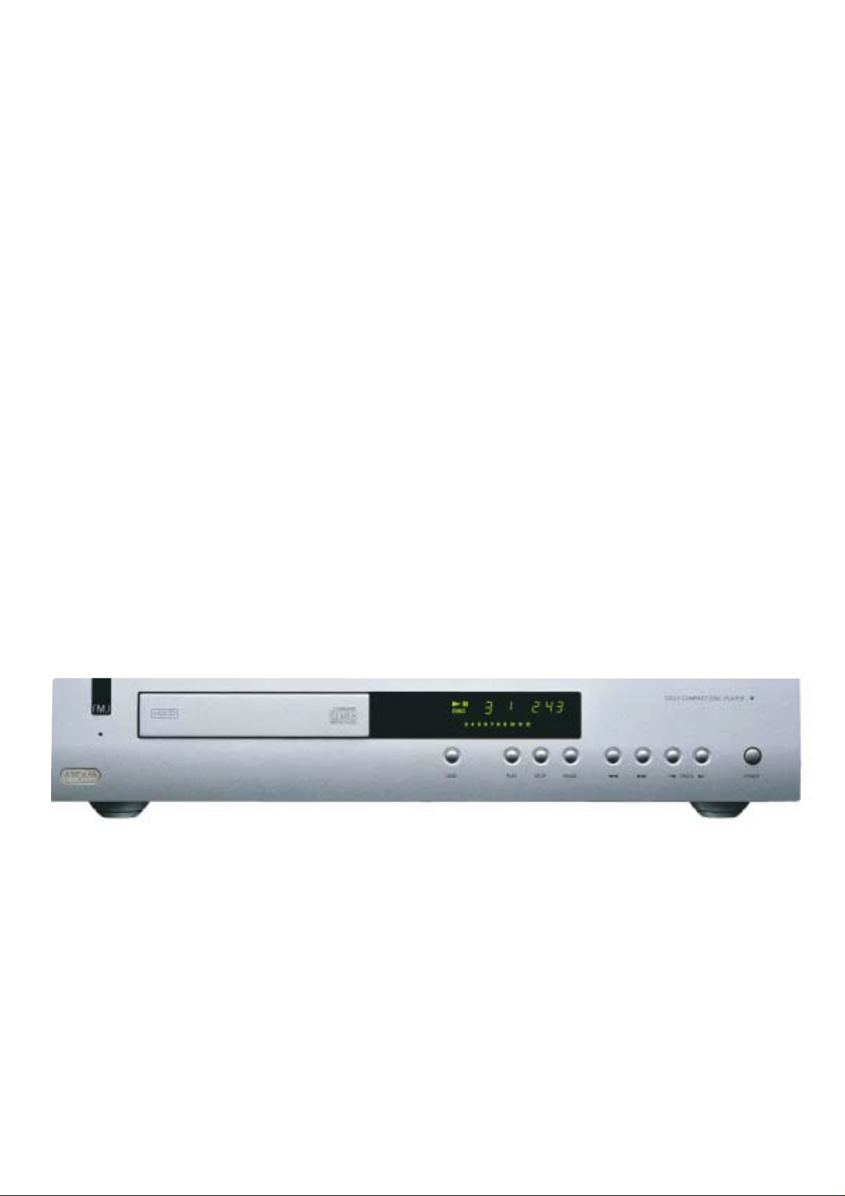
CD23
Issue 1.0
FMJ CD23
Compact Disc Player (Text)
ARCAM
Page 2

Contents List
!
Service guide
o Fault diagnostics
o Power supply test points
o Hints & tips
!
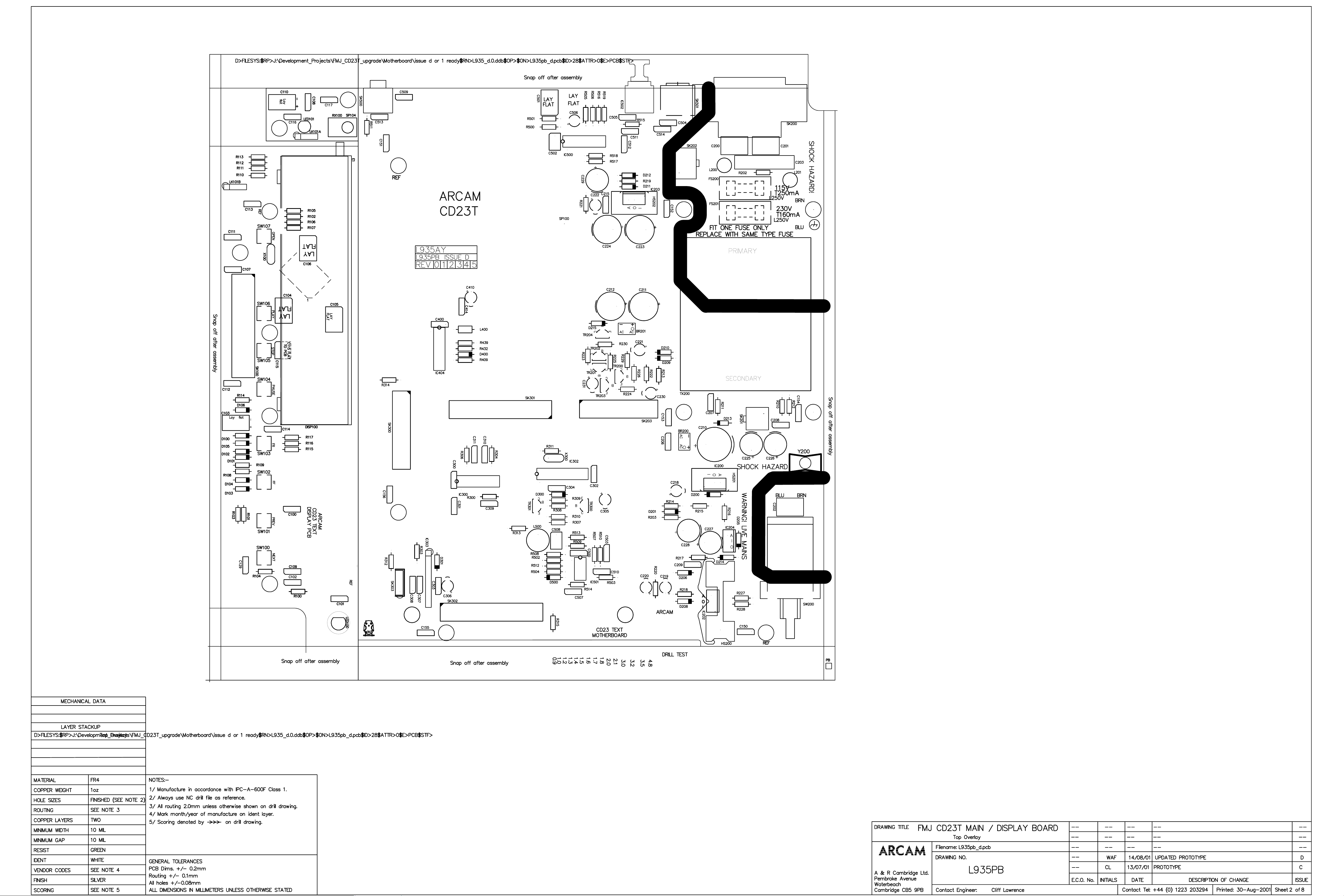
Main board L935
o Circuit description
o Component overlay
o Parts list
o Circuit diagrams
!
DAC board L912
o Circuit description
o Component overlay
o Parts list
o Circuit diagrams
!
Transformer specifications
o L859TX
o L860TX
o L883TX
!
General assembly
o Parts list
Page 3

Service Guide
Contents
!
!
!
Fault diagnostics
Power supply test
points
Hints & tips
Page 4
CD23 (Text) Service Guide
Fault diagnostics
Fault Action
No power Check mains fuse
Check power supply rails
No Audio output Check for digital output, if ok then
check power supply voltages
Check DAC chip
Intermittent noise on output Check Dac chip
Fails to respond to commands Check supply to remote circuit
Check remote flex foil cable
Check for +4.9volts on RX201 o/p
Fails to read disc Check mech supply
Check clock signal
Laser optic moves to end stop
position
No Display Check filament voltage 3.1vac
Spurious display readout Check for dry joints on display board
Power supply test points
Position Voltage
DGND 0 volts
PL202 +12 volts
PL204 -12 volts
IC200 o/p +7.3 volts - mech supply
IC203 o/p +5 volts - DAC supply
IC202 o/p +5 volts - Digital supply
IC204 o/p -30 volts
Between R227 & R228 3.1 volts AC – display filament
Hints & tips
!
Voltage conversion 230/115VAC by changing the internal fuse position and fitting the correct
rated fuse. 100VAC requires a different transformer.
Caused by failure of clock signal to
the mech
Check mech supply
Check clock signal
Check flex foil cable
Check for dry joints on micro and
display
Page 5

Main
Board
L935
Contents
!
Circuit description
!
Component overlay
!
Parts list
!
Circuit diagrams
Page 6

CD23 (text) Circuit Description
Power Supplies Transformers
115/230 VAC:
! Main board - part number L859TX
! Toroid - part number L860TX
100 VAC:
! Main board - part number L862TX
! Toroid - part number L883TX
Main board transformer secondary windings:
1. 9V-0V-32V to produce the digital, motor drive and
2. 0-5V to provide an AC supply for the display
Toroid transformer secondary winding:
1. 13.7-0V-13.7 for audio output circuitry (DAC)
Relay Mute Control
This circuit drives a relay to un-mute the analogue output ~5
seconds after the unit is powered on, and quickly mutes the
output when the unit is switched off. Th e cir cu it works
effectively as an “AND” gate.
If AC is present on the transformer secondary winding and the 5second timer composed of R222 and C221 has reached the
threshold voltage (Vbe of TR200 + Vbe of TR201 - Vce of
TR202, or ~1.0V), the relay coil is connected to +11V
(referenced to 0V_3 as required by the DAC’s internal circuitry)
via TR204.
When AC is removed, C231 discharges quickly through R225,
the base voltage of TR204 rises and the relay coil voltage is
removed, mutin g t he output .
TR203 resets the ‘timer’ by discharging C221 quickly at turn-off.
Remote Control/PIC Micro
Remote control data is received from the IREy e on the display PCB
and buffered by TR300 and TR301. The Programmable Interrupt
Controller converts the RC-5 format data into the NEC format
required by the Sony micro. The PIC al so control s the con fig ura tio n
of the digital filter/DAC on the DAC board.
Motor Driver
The status of the drawer is indicated to the micro by two micro
switches ‘INSW’ and ‘OUTSW’ on SK205. The micro controls
the drawer motor via driver IC303.
fluorescent display grid supplies
+11V(U) Unregulated supply for relay drive and
+5V(D) supply
+7V (IC200) Mechanism and motor driver
supply
+5V(D) (IC202) General digital logic supply
+5V(A) (IC203) Supply to DAC
-30V (IC204) Display grid voltage.
filament.
Clock Buffering
The clock and data signals LRCK, ADATA and BCLK from the
mechanism connector SK300 are double buffered by IC300
before being delivered to the DAC.
Power-On/Reset
The power-on reset signal XRST (or RESET) is generated by
R409, C410 and IC404. When the power is turned on, C410 is
initially uncharged and pin 11 of IC404 is at high voltage, and
thus the output is low. After a short time, C410 is charged via
R409; IC404 pin 11 is then low, and the output switches high
(RESET is de-asserted).
System Clock
The system clock is generated on the DAC board.
The clock and data signals LRCK, ADATA and BCLK from the
mechanism connector SK300 are double buffered by IC300 before
being delivered to the DAC. The system clock is delivered to the
mech via two-position jumper PL300.
Microcontroller & Display Board
The system microcontroller IC100 serves the following functions:
! Control of the mechanism & decoder on the CDM14
mechanism
! Control of mute, attenuation and de-emphasis for the
DAC
! Direct drive of the fluorescent display
! Remote control decoding
! Keyboard scanning
! DAC muting
The keyboard scanning works by connecting the keys to a resistor
ladder on an ADC input to the micro. Pressing a key presents a
unique voltage to this input, which the micro is pre-programmed
to interpret accordingly.
The remote control data contains a ‘Customer Code’ that
identifies this as an Arcam product. The diode network D100 to
D106 configures the micro to accept this code.
Remote Bus Carrier Filter & Demodulator
Remote control commands can be delivered over wire to SK500
for multi-room applications. Incoming signals are attenuated and
clipped by resistors and D500. L500 and C508 form a parallel
resonant circuit at approximately 37kHz. This demodulates the
incoming signal and the output is passed to IC501A where it is
‘chopped’, low pass filtered and fed to IC501B to provide the
RC5 outp ut signal.
Digital Output
The decoder on the mechanism assembly generates an SPDIF
format digital output signal. This is passed to buffer IC500A.
IC500B through E are used in parallel to provide a transformer
less 75-ohm source impedance to a single phono socket SK501.
Optical digital output via IC502 is also tapped off the digital
output signal via IC500F.
Page 7
CAM Products 2000(TM):
Page 8

L935 Main Board Parts List Issue 4.0
Designator Part Description
BR200 3BDF01M Bridge rectifier DF01M 1A 100V
BR201 3BDF01M Bridge rectifier DF01M 1A 100V
C100 2A210 CERD 1N0 63V 20% RA
C101 2A210 CERD 1N0 63V 20% RA
C102 2A210 CERD 1N0 63V 20% RA
C103 2N710 ELST 100U 25V
C103 2P710ZA ELST 100U 25V ZA RUBYCON
C104 2A410 CERD 100N 63V 20% RA
C105 2A410 CERD 100N 63V 20% RA
C106 2A410 CERD 100N 63V 20% RA
C107 2A410 CERD 100N 63V 20% RA
C108 2A410 CERD 100N 63V 20% RA
C109 2A410 CERD 100N 63V 20% RA
C110 2N610 ELST 10U 50V
C111 2A210 CERD 1N0 63V 20% RA
C112 2A410 CERD 100N 63V 20% RA
C113 2A210 CERD 1N0 63V 20% RA
C114 2A210 CERD 1N0 63V 20% RA
C115 2A210 CERD 1N0 63V 20% RA
C116 2A210 CERD 1N0 63V 20% RA
C117 2A210 CERD 1N0 63V 20% RA
C129 2A310 CERD 10N 63V 20% RA
C151 2A210 CERD 1N0 63V 20% RA
C152 2A210 CERD 1N0 63V 20% RA
C153 2A210 CERD 1N0 63V 20% RA
C154 2A210 CERD 1N0 63V 20% RA
C155 2A210 CERD 1N0 63V 20% RA
C156 2A210 CERD 1N0 63V 20% RA
C200 2K233 SUPPR CAP 3N3 250V
C201 2K233 SUPPR CAP 3N3 250V
C202 2K233 SUPPR CAP 3N3 250V
C203 2D422 220NF CLASS X2 CAP 275VRMS
C206 2A410 CERD 100N 63V 20% RA
C207 2A410 CERD 100N 63V 20% RA
C208 2A410 CERD 100N 63V 20% RA
C209 2A410 CERD 100N 63V 20% RA
C210 2N833 ELST 3M3 25V
C211 2N810 ELST 1M0 25V
C212 2N810 ELST 1M0 25V
C215 2K410 PEST 100N 63V 10%
C218 2N710 ELST 100U 25V
C219 2N710 ELST 100U 25V
C220 2N710 ELST 100U 25V
C221 2N710 ELST 100U 25V
C222 2N710 ELST 100U 25V
C223 2N810 ELST 1M0 25V
C224 2N810 ELST 1M0 25V
C225 2N710B ELST 100U 100V
C226 2N710B ELST 100U 100V
C227 2N710B ELST 100U 100V
C228 2N810A ELST 1M0 10V
C229 2N810A ELST 1M0 10V
C230 2N710 ELST 100U 25V
C231 2N610 ELST 10U 50V
C300 2A410 CERD 100N 63V 20% RA
Page 9

L935 Main Board Parts List Issue 4.0
Designator Part Description
C301 2A410 CERD 100N 63V 20% RA
C302 2A410 CERD 100N 63V 20% RA
C303 2A410 CERD 100N 63V 20% RA
C304 2A110 CERD 100P 50V -20% +80% RA
C305 2N710 ELST 100U 25V
C306 2N710 ELST 100U 25V
C307 2A310 CERD 10N 63V 20% RA
C308 2A410 CERD 100N 63V 20% RA
C400 2A410 CERD 100N 63V 20% RA
C410 2N710 ELST 100U 25V
C414 2A410 CERD 100N 63V 20% RA
C500 2A410 CERD 100N 63V 20% RA
C501 2A310 CERD 10N 63V 20% RA
C502 2K447 PEST 470N 63V 10%
C503 2A210 CERD 1N0 63V 20% RA
C504 2A310 CERD 10N 63V 20% RA
C505 2A410 CERD 100N 63V 20% RA
C506 2P622 ELST 22U 20V OSCON
C507 2A410 CERD 100N 63V 20% RA
C508 2D168 PPRO 680P 5% 63V RA
C509 2A410 CERD 100N 63V 20% RA
C510 2A110 CERD 100P 50V -20% +80% RA
C511 2A410 CERD 100N 63V 20% RA
C512 2A147 CERD 470P 50V -20% +80% RA
C513 2A110 CERD 100P 50V -20% +80% RA
C514 2A410 CERD 100N 63V 20% RA
CA1 L920CA CD...T MAINS JUMPER CABLE
D100 3A4148 SSDIODE 1N4148 75V
D101 3A4148 SSDIODE 1N4148 75V
D102 3A4148 SSDIODE 1N4148 75V
D103 3A4148 SSDIODE 1N4148 75V
D104 3A4148 SSDIODE 1N4148 75V
D105 3A4148 SSDIODE 1N4148 75V
D106 3A4148 SSDIODE 1N4148 75V
D200 3A4148 SSDIODE 1N4148 75V
D201 3A4148 SSDIODE 1N4148 75V
D205 3A4148 SSDIODE 1N4148 75V
D206 3A4148 SSDIODE 1N4148 75V
D208 3A4148 SSDIODE 1N4148 75V
D209 3A4148 SSDIODE 1N4148 75V
D210 3A4148 SSDIODE 1N4148 75V
D211 3A4148 SSDIODE 1N4148 75V
D212 3A4148 SSDIODE 1N4148 75V
D213 3B4003 RECTIFIER 1N4003F 1A 200V
D214 3C05104 Diode 5V1 400mW
D215 3A4148 SSDIODE 1N4148 75V
D300 3A4148 SSDIODE 1N4148 75V
D301 3C04704 ZENER 4V7 400MW
D400 3A4148 SSDIODE 1N4148 75V
D500 3C04704 ZENER 4V7 400MW
DISP100 B1015 DISP CD SONY 14-ST-20GK
E1 E930MC CD23TEXT VFD SUPPORT
EL200 8M101 EARTH LEAD
FS200 F022 INS COVER PCB FUSEHOLDER
FS200 8S004 FUSEHOLDER 20mm PCB
Page 10

L935 Main Board Parts List Issue 4.0
Designator Part Description
FS201 C11166 FUSE 20mm 160mA T S504160mA
FS201 F022 INS COVER PCB FUSEHOLDER
FS201 8S004 FUSEHOLDER 20mm PCB
HS200 F006 HEATSINK CLIP TO220 13/8.6 DC/W
HS200 F008 HEATSINK TO220 8.6 DEGC/W
HS201 F007 HEATSINK TO220 CLIP 30
HS202 F007 HEATSINK TO220 CLIP 30
IC100 5G82832 IC CD CXP82832-031Q MICRO
IC200 5D1086A IC VREG LM1086CT-ADJ
IC202 5D317T IC VREG POS LM317T
IC203 5D317T IC VREG POS LM317T
IC204 5D337 IC VREG POS LM337T
IC300 5J7404 IC HCMOS 74HCU04
IC302 5H16C54X IC CMOS MICRO PIC16C54XT/P
IC302 8S018 IC SOCKET 18 PIN 0.3''
IC302 5H16C54X IC CMOS MICRO PIC16C54XT/P
IC303 5Q1641 IC MOTOR DRIVER LB1641
IC404 5J7404 IC HCMOS 74HCU04
IC500 5J7404 IC HCMOS 74HCU04
IC501 5M393A IC COMPARITOR DUAL LM393A
IC502 5TG550T SPDIF OPTICAL TRANSMITTER
IC302SW L825SW SOFTWARE
IC302SW L825SW SOFTWARE
L200 7D968A 6U8H INDUCTOR
L201 7D968A 6U8H INDUCTOR
L400 7F003 FERRITE BEAD SINGLE AXIAL TAPED 2K BOX
L500 7D327 27mH INDUCTOR
LED100 3D001 LED GREEN 5MM
LED101 3D003 LED ULTRARED 5MM
LK101A L814CA JUMPER 4-WAY LEAD
MC200 E922MC MAGNETIC SHIELD PLATE (ATTACH TO TX WITH E923MC)
MC201 E923MC ADHESIVE PAD (ATTACH TO E922MC & TX)
PCB L935PB_3 PRINTED CIRCUIT BOARD
PCB L935PB_2 PRINTED CIRCUIT BOARD
R100 1H122 RES MF W4 220R 1%
R101 1H310 RES MF W4 1% 10K
R102 1H310 RES MF W4 1% 10K
R103 1H268 RES MF W4 1% 6K8
R104 1H268 RES MF W4 1% 6K8
R105 1H268 RES MF W4 1% 6K8
R106 1H268 RES MF W4 1% 6K8
R107 1H268 RES MF W4 1% 6K8
R108 1H233 RES MF W4 1% 3K3
R109 1H222 RES MF W4 1% 2K2
R110 1H215 RES MF W4 1% 1K5
R111 1H210 RES MF W4 1% 1K0
R112 1H168 RES MF W4 1% 680R
R113 1H010 RES MF W4 1% 10R
R114 1H310 RES MF W4 1% 10K
R115 1H310 RES MF W4 1% 10K
R116 1H310 RES MF W4 1% 10K
R117 1H310 RES MF W4 1% 10K
R202 1K515 RES W25 5% VR25 1M5
R203 1H133 RES MF W4 1% 330R
R210 1G810 RES MF FU W3 1R0 5% NFR25
Page 11

L935 Main Board Parts List Issue 4.0
Designator Part Description
R211 1G010 RES MF FU W3 10R 5% NFR25
R212 1G810 RES MF FU W3 1R0 5% NFR25
R213 1G010 RES MF FU W3 10R 5% NFR25
R214 1H216 RES MF W4 1% 1K6
R215 1H322 RES MF W4 1% 22K
R216 1H210 RES MF W4 1% 1K0
R217 1H333 RES MF W4 1% 33K
R218 1H127 RES MF W4 1% 270R
R219 1H127 RES MF W4 1% 270R
R220 1H182 RES MF W4 1% 820R
R221 1H182 RES MF W4 1% 820R
R222 1H447 RES MF W4 1% 470K
R223 1H310 RES MF W4 1% 10K
R224 1H310 RES MF W4 1% 10K
R225 1H222 RES MF W4 1% 2K2
R226 1H310 RES MF W4 1% 10K
R227 1H110 RES MF W4 1% 100R
R228 1H110 RES MF W4 1% 100R
R229 1H215 RES MF W4 1% 1K5
R230 1H310 RES MF W4 1% 10K
R300 1H056 RES MF W4 1% 56R
R303 1H268 RES MF W4 1% 6K8
R304 1H056 RES MF W4 1% 56R
R306 1H056 RES MF W4 1% 56R
R307 1H310 RES MF W4 1% 10K
R308 1H310 RES MF W4 1% 10K
R309 1H310 RES MF W4 1% 10K
R310 1H310 RES MF W4 1% 10K
R311 1H410 RES MF W4 1% 100K
R312 1H268 RES MF W4 1% 6K8
R313 1H410 RES MF W4 1% 100K
R314 1H310 RES MF W4 1% 10K
R315 1H310 RES MF W4 1% 10K
R409 1H310 RES MF W4 1% 10K
R432 1H310 RES MF W4 1% 10K
R439 1H510 RES MF W4 1% 1M0
R500 1H010 RES MF W4 1% 10R
R501 1H010 RES MF W4 1% 10R
R502 1H218 RES MF W4 1% 1K8
R503 1H218 RES MF W4 1% 1K8
R504 1H210 RES MF W4 1% 1K0
R505 1H112 RES MF W4 1% 120R
R506 1H212 RES MF W4 1% 1K2
R507 1H310 RES MF W4 1% 10K
R508 1H310 RES MF W4 1% 10K
R509 1H310 RES MF W4 1% 10K
R510 1H310 RES MF W4 1% 10K
R511 1H147 RES MF W4 1% 470R
R512 1H410 RES MF W4 1% 100K
R513 1H410 RES MF W4 1% 100K
R514 1H215 RES MF W4 1% 1K5
R515 1H310 RES MF W4 1% 10K
R516 1H212 RES MF W4 1% 1K2
R517 1H212 RES MF W4 1% 1K2
R518 1H212 RES MF W4 1% 1K2
Page 12

L935 Main Board Parts List Issue 4.0
Designator Part Description
R519 1H110 RES MF W4 1% 100R
RX100 B2107 REMOTE RX PIC-26043TM2
SK100 8K8132 32-WAY FFC CONN HORIZ
SK200 8A001 IEC MAINS CONN PCB INS PX
SK200 HP007 COPPER RIVET TCP/D48 BS
SK201 8K2304 MOLEX MINI FIT 4 WAY
SK202 8K2306 MOLEX MINI FIT HCS 6 WAY
SK203 8K8023 23-WAY FFC CONN VERT
SK300 8K8023 23-WAY FFC CONN VERT
SK301 8K8032 32-WAY FFC CONN VERT
SK302 8K8032 32-WAY FFC CONN VERT
SK303 8K2005 5-WAY AMP CT CONN
SK500 8D228 MIN JACK SINGLE 3.5mm
SK501 8D220 PHONO SKT SINGLE EMC
SP103 F215 DS STICKY PAD 70 X 25mm
SP104 E822AP IR RX SUPPORT PAD
SW100 A1510 TACT SWITCH 2-PIN LOW PROF NO GND PIN
SW101 A1510 TACT SWITCH 2-PIN LOW PROF NO GND PIN
SW102 A1510 TACT SWITCH 2-PIN LOW PROF NO GND PIN
SW103 A1510 TACT SWITCH 2-PIN LOW PROF NO GND PIN
SW104 A1510 TACT SWITCH 2-PIN LOW PROF NO GND PIN
SW105 A1510 TACT SWITCH 2-PIN LOW PROF NO GND PIN
SW106 A1510 TACT SWITCH 2-PIN LOW PROF NO GND PIN
SW107 A1510 TACT SWITCH 2-PIN LOW PROF NO GND PIN
SW200 A1010 SWITCH PUSH MAINS DPST TV-8
TR200 4A549 TRANS LF SS N BC549B
TR201 4A549 TRANS LF SS N BC549B
TR202 4A549 TRANS LF SS N BC549B
TR203 4A549 TRANS LF SS N BC549B
TR204 4A557 TRANS LF SS P BC557B
TR300 4A549 TRANS LF SS N BC549B
TR301 4A549 TRANS LF SS N BC549B
TX200 L859TX FMJ COOL MULTI-VOLTAGE TX
TX200 L859TX FMJ COOL MULTI-VOLTAGE TX
X100 7W008 CER RESON 8.00MHz
X300 7W005 CER RESON 4.00MHz
Y200 F185 TX WIRE RESTRAINT
Y200 F185 TX WIRE RESTRAINT
Y201 HF4V09B SCREW
Y202 HF4V09B SCREW
Y203 HF4V09B SCREW
Y204 HF4V09B SCREW
Page 13
POWER SUPPLIES MECH INTERCONNECTS DAC AND OSCILLATOR
L935C2_4
L935C2_4.0.sch
FILA
FILB
L935C3_4
L935C3_4.0.sch
FILA
FILB
17MHZ
RESET
BCLK
ADATA
LRCKRC5 IP
DIGOP
EMPHASIS
L935C4_4
L935C4_4.0.sch
DEEM
LRCK
ADATA
BCLK
RESET
17MHZ
FIX152
FIXING HOLE 3.5
(EARTH BY IEC SOCKET)
DISPLAY PCB
L935C1_4
L935C1_4.0.sch
FIX157
FIXING HOLE 3.2
C150
1N0 CD
0V_DIG 0V_DIG 0V_DIG 0V_DIG 0V_DIG 0V_DIG 0V_DIG
EMC2
PCB
PCB
L935PB_4
FIX151
FIXING HOLE 3.2
EMC1
IC302SW
S/W
L825SW
C151
1N0 CD
FIX153
FIXING HOLE 3.5
RC5 INPUT AND DIG OUTPUTS
L935C5_4
L935C5_4.0.sch
DIGOP RC5RP
FIX154
FIXING HOLE 3.5
C152
1N0 CD
C153
1N0 CD
FIX155
FIXING HOLE 3.5
C154
1N0 CD
FIX156
FIXING HOLE 3.5
C155
1N0 CD
FIX150
FIXING HOLE 3.5
C156
1N0 CD
0V_DIG
0V_MOT
0V_30V_DIG
0V_2
SP100
STARPOINT
0V_1
USE EXCLUDE NF WHEN GENERATING ROS.
DRAWING TITLE
23425
A & R Cambridge Ltd.
Pembroke Avenue
Waterbeach
Cambridge CB5 9PB
CD23T - TOP LEVEL SCHEMATIC
Filename:
Notes:
Contact Engineer:
L935C6_4.0.prj
Contact Tel: (01223) 203 200Travis Pierce
ECO No. DESCRIPTION OF CHANGE
INITIALS
Printed: 6 6Sheet of
DATE
23-Jan-2002
DRAWING NO.
4.0PCB REMOTE SNAP OFF CHANGEWAF 22/1/0202_E011
3.0ADMINISTRATIVE ISSUE CHANGE, PCB TO ISS3 FOR AIWA REQCL 04/10/0101_1171
ISSUE
L935CT
Page 14

SK200
IEC3
N E L
N
E
C200
C201
3N3(X1Y2)
R202
NEUTRAL LIVE
L200
6U8H
1M5 VR25
C203
220N(X2)
NEUTRAL2
SK202
3
2
1
6
5
4
MOLEXPWR6
(FOR AUX TOROID)
CA1
L920CA
L
3N3(X1Y2)
L920CA
BRN BRN
L201
6U8H
BLU
BLU
LIVE2
EL200
EARTH LEAD
8M101
EARTH LEAD
(IEC INLET TO CHASSIS)
SW200A
MAINS_SW A1010
SW200B
MAINS_SW A1010
EMC2
C202
3N3(X1Y2)
EMC2
FS200
T250MA115V
115V ONLY
FS201
T160MA
230V ONLY
NEUTRAL2
115V
115V
230V
230V
1
2
7
6
4
5
10
9
TX200
L859TX
NB: A CABLE GOES BETWEEN BRN BRN AND BLU BLU
FROM MAINS SWITCH TO BACK OF PCB
Y200
TX WIRE CLIP
FILA
FILB
SK201
MOLEXPWR4
(FOR AUX TOROID)
1
2
3
4
TX_16
BR201
DF01M
+
C211
1M0 25V
+
C223
1M0 25V
+12V(A)
D200
1N4148
IC200
+11V(U)
BR200
DF01M +
D213
1N4003
C210
3M3 EL
+
C225
100U EL 100V
AC_3
TX_19
R210
TX_20
AC1
C206
100N CD
R211
10R FU
1R0 FU
R212
AC2
C207
100N CD
C208
100N CD
11
13
15
19
20
1R0 FU
R227
100R MF
R228
LM1086-ADJ
I
Vin
I
Vin
IC204
ADJ
A
+
C218
100U EL
+
C226
100U EL 100V
A
ADJ
LM337T
D205
1N4148
Vout
Vout
O
O
TX_18
HS201
TO220HS30REG
R203
330R MF
R214
1K6 MF
R215
22K MF
R216
1K0 MF
D201
1N4148
-30VF
+
+7V
+
C227
100U EL 100V
Filiament supply
Motor drive supply
C228
1M0 10V
R217
33K MF
0V_2
D214
5V1 400MW
+
C212
1M0 25V
+
C224
1M0 25V
100R MF
0V_1
-12V(A)
+11V(U)
IC202
I
Vin
C209
100N CD
HS
D206
1N4148
LM317T
A
ADJ
+
C219
100U EL
Vout
HS200
TO220HS08REG
O
R218
270R MF
R220
820R MF
D208
1N4148
+5V(D)
0V_2
Digital +5V
+
C220
100U EL
D211
TX FIXING SCREWS
Y201
SCREW HF4V09B
Y203
SCREW HF4V09B
Y202
SCREW HF4V09B
Y204
SCREW HF4V09B
AFFIX TO TX BETWEEN ANALOGUE CIRCUITRY & TX
MC200
E922MC
E922MC
MC201
E923MC
E923MC
AC1
AC2
D209
1N4148
D210
1N4148
R213
10R FU
C230
100U EL
0V_3
1N4148
IC203
I
Relay control for AC detect
R222
470K MF
C221
100U EL
R226
10K MF
R229
TR200
BC549B
+
1K5 MF
TR201
BC549B
TR204
BC557B
R230
10K MF
D215
1N4148
0V_3
R224
10K MF
+
C231
10U EL
R223
10K MF
R225
+
2K2 MF
TR202
BC549B TR203
BC549B
+12V(A)
-12V(A)
+5V(A)
+5V(D)
RLYPWR
+11V(U)
SK203
23
22
21
20
19
18
17
16
15
14
13
12
11
10
9
8
7
6
5
4
3
2
1
FFC23V
Power connector for 9DAC PCB
Vin
C215
100N PE
LM317T
A
ADJ
+
C222
100U EL
Vout
O
HS202
TO220HS30REG
R219
270R MF
R221
820R MF
D212
1N4148
+5V(A)
0V_1
DAC supply
+
C229
1M0 10V
0V_DIG
0V_3
DRAWING TITLE
CD23T - POWER SUPPLIES
23425
A & R Cambridge Ltd.
Pembroke Avenue
Waterbeach
Cambridge CB5 9PB
Filename:
Notes:
Contact Engineer:
L935C2_4.0.sch
4.0PCB REMOTE SNAP OFF CHANGEWAF 22/1/0202_E011
3.0ADMINISTRATIVE ISSUE CHANGE, PCB TO ISS3 FOR AIWA REQCL 04/10/0101_1171
ECO No. DESCRIPTION OF CHANGE
Contact Tel: (01223) 203 200Travis Pierce
INITIALS
Printed: 2 6Sheet of
DATE
23-Jan-2002
DRAWING NO.
L935CT
ISSUE
Page 15

+5V(D)
Data connector to DAC PCB
SK301
FFC32V
24
25
26
27
28
29
30
31
32
Flexfoil connector to Display PCB
SK302
FFC32V
+5V(D)
10
11
12
13
14
15
16
17
18
19
20
21
22
23
123456789
30
31
32
25
26
27
28
29
20
21
22
23
24
15
16
17
18
19
10
11
12
13
14
123456789
DIGOP
14
7
SK300
FFC23V
IC300G
74HCU04
23
22
21
20
19
18
17
16
15
14
13
12
11
10
9
8
7
6
5
4
3
2
1
R314
10K MF
CLK
XRST
DATA
LDON
SENS
XLT
SUBQ
SQCK
AMUTE
BCLK
SCOR
ADATA
LRCK
LPH
0V_DIG
R307
10K MF
C300
100N CD
0V_DIG
Flex connector from CDM14BL-5BD25 mech
+5V(D)
0V_DIG
+7V
0V_DIG
IREYE
RC5 IP
C301
100N CD
R310
10K MF
IC300A
BCLK
1 2
74HCU04
ADATA
LRCK
17MHz Master Clock
R308
10K MF
TR300
BC549B
5 6
IC300E
74HCU04
+5V(D)
IC300C
74HCU04
R309
10K MF
TR301
BC549B
IC300B
3 4
74HCU04
IC300D
74HCU04
IC300F
1011
74HCU04
(From 9 DAC PCB)
89
1213
D300
1N4148
C304
100P CD
+5V(D)
0V_DIG
R300
56R MF
R304
56R MF
R306
56R MF
RA0
AMUTE
DEEM
RMIN
XRST
0V_DIG
0V_DIG
0V_DIG
RESET
R311
100K MF
C309
10P CD
NF
C310
10P CD
NF
C311
10P CD
NF
+5V(D)
R313
100K MF
IC302
PIC16C54XT
17
RA0
18
RA1
1
RA2
2
RA3
3
RTCC
4
MCLR
16
OSC1
X300
CST4.00
0V_DIG
AMUTE
OSC2
15
XRST
VSS
5
RB0
RB1
RB2
RB3
RB4
RB5
RB6
RB7
DEEM
VDD
14
RA0
6
7
8
9
10
11
12
13
C302
100N CD
RB6
+5V(D)
RB5
RB0
RB4
RB5
RB6
+
C305
100U EL
RB4
RB0
HDCD
0V_DIG
Motor Drive
IC303
LB1641
O/P 'Out'
LoadOut
O/P 'In'
Vcc
Vcc
LoadIn
Bias
GND
FILA
10
9
8
7
6
5
4
3
2
1
SCOR
0V_DIG
LDOUT
LDIN
D301
4V7 400MW
RMIN
LDOUT
C303
100N CD
LDIN
SENS
+7V
0V_MOT
XLT
+
AMUTE
C306
100U EL
CLK
LDON
C307
10N CD
C308
100N CD
DATA
SQCK
SUBQ
LOADSW
-30VF
0V_MOT
XRST
HDCD
DEEM
+5V(D)
LPH
R303
6K8 MF
LOADSW
R312
6K8 MF
IREYE
FILB
0V_DIG
R315
10K MF
SK303
8K2005
1
2
3
4
5
EMPHASIS
LOADOUT
LOADIN
GND
INSW
OUTSW
0V_DIG
DRAWING TITLE
23425
A & R Cambridge Ltd.
Pembroke Avenue
Waterbeach
Cambridge CB5 9PB
CD23T - MECH, MOTOR & MICRO
Filename:
Notes:
Contact Engineer:
L935C3_4.0.sch
Contact Tel: (01223) 203 200Travis Pierce
ECO No. DESCRIPTION OF CHANGE
INITIALS
Printed: 3 6Sheet of
DATE
23-Jan-2002
DRAWING NO.
4.0PCB REMOTE SNAP OFF CHANGEWAF 22/1/0202_E011
3.0ADMINISTRATIVE ISSUE CHANGE, PCB TO ISS3 FOR AIWA REQCL 04/10/0101_1171
ISSUE
L935CT
Page 16

C400
100N CD
L400
7F003
14
IC404G
74HCU04
7
C414
100N CD
D400
1N4148
+5V(D)
+
C410
100U EL
R409
10K MF
R432
10K MF
R439
1M0 MF
IC404E
74HCU04
1011
IC404F
74HCU04
1213
1 2
IC404A
74HCU04
3 4
IC404B
74HCU04
5 6
IC404C
74HCU04
IC404D
74HCU04
0V_DIG
0V_DIG
89
RESET
DRAWING TITLE
CD23T - RESET CIRCUIT
23425
A & R Cambridge Ltd.
Pembroke Avenue
Waterbeach
Cambridge CB5 9PB
Filename:
Notes:
Contact Engineer:
L935C4_4.0.sch
4.0PCB REMOTE SNAP OFF CHANGEWAF 22/1/0202_E011
3.0ADMINISTRATIVE ISSUE CHANGE, PCB TO ISS3 FOR AIWA REQCL 04/10/0101_1171
ECO No. DESCRIPTION OF CHANGE
Contact Tel: (01223) 203 200Travis Pierce
INITIALS
Printed: 4 6Sheet of
DATE
23-Jan-2002
DRAWING NO.
L935CT
ISSUE
Page 17

CARRIER FILTER AND DEMODULATOR
+5V(D)
SK500
JACK3.5
C509
100N CD
EMC1
R511
470R MF
C513
100P CD
R504
1K0 MF
0V_DIG
+5V(D)
R500
10R MF
0V_DIG
R512
100K MF
D500
4V7 400MW
RC5RP
C502
470N PE
DIGOP
IC500G
7
74HCU04
R507
10K MF
14
1 2
IC500A
74HCU04
L500
27mH
7
IC501B
LM393A
C508
680P PP
5
6
C510
100P CD
IC500F
74HCU04
IC500E
74HCU04
IC500D
74HCU04
5 6
IC500C
74HCU04
3 4
IC500B
74HCU04
R508
10K MF
1213
1011
89
R502
1K8 MF
R514
1K5 MF
R503
1K8 MF
R505
120R MF
R506
1K2 MF
R516
1K2 MF
R517
1K2 MF
R518
1K2 MF
2
3
IC501A
LM393A
C507
100N CD
R510
10K MF
R519
100R MF
1
R509
10K MF
R513
100K MF
+5V(D)
R501
10R MF
GP1FA550TZ
IC502
C512
470P CD
C503
1N0 CD
1
84
OPTICAL OUTPUT
2
VCC
I/P
GND
3
100N CD
R515
10K MF
C505
C511
IC501C
LM393A
C501
10N CD
SK501
PHONO1
EMC
C500
100N CD
0V_DIG
+ C506
22U EL OS
COAXIAL OUTPUT
C504
10N CD
C514
100N CD
0V_DIG
DRAWING TITLE
23425
A & R Cambridge Ltd.
Pembroke Avenue
Waterbeach
Cambridge CB5 9PB
100N CD
CD23T - RC5 INPUT & DIGITAL OUT
Filename:
Notes:
Contact Engineer:
L935C5_4.0.sch
Contact Tel: (01223) 203 200Travis Pierce
ECO No. DESCRIPTION OF CHANGE
INITIALS
Printed: 5 6Sheet of
DATE
23-Jan-2002
DRAWING NO.
4.0PCB REMOTE SNAP OFF CHANGEWAF 22/1/0202_E011
3.0ADMINISTRATIVE ISSUE CHANGE, PCB TO ISS3 FOR AIWA REQCL 04/10/0101_1171
ISSUE
L935CT
Page 18

FIX107
FIXING HOLE 3.5
C116
1N0 CD
0VREM
(NEAR SK100)
FIX108
FIXING HOLE 3.2
C117
1N0 CD
0VREM
+5V
+
C103
100U EL
LK101A
1
2
3
4
L814CA
C112
100N CD
+5VREM
IREYEREM
RX100
PIC-26043TM2
3
O/P
+5V
GND
2
C105
100N CD
1
HDCD LED
LED101
LED ULTRARED
DECOUPLING CAPACITORS FOR IC100
C104
100N CD
C106
100N CD
C108
100N CD
R100
220R MF
+5VREM
+
C110
10U EL
0VREM
LED100
LED GREEN
POWER LED
SP104
IR RX
SUPPORT PAD
IR RX SUPPORT PAD
CMO4
D100
1N4148
D101
1N4148
REMOTE CUSTOM CODE DIODE MATRIX
D102
1N4148
D103
1N4148
D104
1N4148
D106
1N4148
CMO3
CMO2
CMO1
D105
1N4148
DISP100
DISPLAY 14-ST-20GK
F11F1214G413G512G611G710G89G98G107G116G125G134G143G152G161G17NC18P119P220P321P422P523P624P725P826P927P1028P1129P1230P1331P1432P1533P1634P1735P1836P1937P2038P2139F241F2
42
F2F1
0V
SP103
70mm x 25mm
DOUBLE SIDED
STICKY GASKET
70X25_DS STICKY TAPE
E1
CD23TXT VFD SUPPORT
E930MC
1
2
3
4
0V
C107
100N CD
-30V
Connector to main PCB
FIX105
FIXING HOLE 3.5
FIX102
FIXING HOLE 3.5
0V
CHASSIS3
C100
1N0 CD
0V 0V 0V
SK100
FFC32H
32
F1
31
30
SCOR_DISP
29
28
27
26
RMIN_DISP
25
LDOUT_DISP
24
LDIN_DISP
23
SENS_DISP
22
21
XLT_DISP
20
AMUTE_DISP
19
18
17
16
15
14
CLK_DISP
13
LDON_DISP
12
DATA_DISP
11
SQCK_DISP
10
SUBQ_DISP
9
LOADSW_DISP
8
XRST_DISP
7
6
5
DEEM_DISP
4
HDCD_DISP
3
LPH_DISP
2
F2
1
IREYE_DISP
PIN 1 TO LEFT
CABLE POINTING DOWN
FIX106
FIXING HOLE 3.5
C114
1N0 CD
FIX103
FIXING HOLE 3.5
0V
C102
1N0 CD
C115
1N0 CD
FIX100
FIXING HOLE 3.2
0V
C113
1N0 CD
LK101B
L814CA
0V
0V
+5V
1
2
IREYE_DISP
3
4
0V
+5V
-30V
TACTSW A1510
SW100
R113
10R MF
FIX101
FIXING HOLE 3.5
C101
1N0 CD
C109
100N CD
0V
R101
10K MF
SW101
NEXT PREV FF FR PAUSE STOP PLAY OPEN
TACTSW A1510
FIX104
FIXING HOLE 3.5
R103
6K8 MF
SW102
TACTSW A1510
R108
3K3 MF
SW103
TACTSW A1510
R109
2K2 MF
SW104
TACTSW A1510
R110
1K5 MF
SW105
TACTSW A1510
R111
1K0 MF
SW106
TACTSW A1510
DRAWING TITLE
R112
680R MF
SW107
TACTSW A1510
CD23T - DISPLAY AND MICRO
C111
1N0 CD
0V
23425
A & R Cambridge Ltd.
Pembroke Avenue
Waterbeach
Cambridge CB5 9PB
R114
10K MF
R115
10K MF
R116
10K MF
R117
10K MF
0V
+5V
R104
6K8 MF
C129
10N CD
Filename:
Notes:
Contact Engineer:
L935C1_4.0.sch
0V
R105
6K8 MF
R106
6K8 MF
R107
6K8 MF
R102
10K MF
10
11
12
13
14
15
16
17
18
19
20
21
22
23
24
25
26
27
28
29
30
1
2
3
4
5
6
7
8
9
Contact Tel: (01223) 203 200Travis Pierce
13G
14G
NC
CMI1
SCOR
CMI2
CMI3
RMIN
CMI4
NC
NC
LDOUT
LDIN
SENS
XLT
AMUTE
PGML
NC
NC
TIMER
NC
CLK
LDON
DATA
SQCK
SUBQ
NC
AVREF
KEY0
KEY1
98
99
100
10G
11G
12G
KEY231KEY332ADJ/AFADJ
LOADSW
33
34NC35NC36
+5V
871G88
892G903G914G925G936G947G958G969G97
VDD
AVSS37RST38EXTAL39XTAL40VSS41NC42NC43VDD44VDP45NC
-30V
+5V
0V
X100
CST8.00
0V
ECO No. DESCRIPTION OF CHANGE
INITIALS
23-Jan-2002
Printed: 1 6Sheet of
S385S286S1
46
DATE
81
S484S583S682S7
EMPHASIS
NC47LPH48NC49NC
50
S10
S11
S12
S13
S14
S15
S16
S17
S18
S19
S20
S21
NC
NC
NC
NC
NC
NC
NC
NC
CMO4
CMO3
CMO2
CMO1
NC
NC
NC
S8
S9
80
79
78
77
76
75
74
73
72
71
70
69
68
67
66
65
64
63
62
61
60
59
58
57
56
55
54
53
52
51
IC100
CXP82832
CMO4
CMO3
CMO2
CMO1
DRAWING NO.
4.0PCB REMOTE SNAP OFF CHANGEWAF 22/1/0202_E011
3.0ADMINISTRATIVE ISSUE CHANGE, PCB TO ISS3 FOR AIWA REQCL 04/10/0101_1171
ISSUE
L935CT
Page 19

DAC
Board
L912
Contents
!
Circuit description
!
Component overlay
!
Parts list
!
Circuit diagrams
Page 20

DAC Circuit description
Refer to L912 circuit diagrams
The DAC PCB converts Sony format digital audio data at
44.1KHz samp ling rate to unba lanced audi o outputs. There i s a
Pacific Microsonics PMD-200 HDCD filter which is
programmed by a dedicated on board PIC micro (IC406) to
accept a variety of data formats.
Digital Filter/HDCD decoder
The FPGA receives two control lin es from the main board PIC,
RB0 and RB6.
RB5 MS1, Serial data mode se l ect 1. Used just after sw itch- on.
RB4 MS2, Serial data mode se l ect 2. Used just after sw itch- on.
The PMD 200 (IC 400) receives Sony format serial digital audio
data (after re latching) mute and de-emphasis control signals
from the main board. The output from this is 8x over-sampled
filtered audio da ta with a 24 bit word len gth. The HDCD filter
output is in serial form BCKO, WCKO, DOL and DOR.
Data Re-latching
The PMD 200 (IC 400 ) requi res t ha t the in put da ta is ti med with
respect to th e system cloc k, h owever th e data edges a re no t well
defined when clocking at the system clock frequency so a relatching circuit, IC300, IC 401, IC402 and IC403, re-clocks
SER_CLK, SER_DIN and SER_CH to double the bit clock
frequency. The phase of the latching clock is nudged if it’s
rising edge gets t oo close to the bit c lock transitions.
Reset Signal
The XRST reset signal from the mother boa rd is buffered by IC
300D & E to produc e the GO signal. C127 at the in put of the
buffer delays GO from falling when the unit i s switched off so
that the mute relay has chance to close before any clicks occur.
The GO signal en ables t he c lock outpu t, in itia tes PMD 200 and
FPGA programming and enables power and bias to the DAC
ASIC.
Power Supplies
TR7 and TR5 regulate the supply to +/-13V with about 0.2V
drop-out margin.
Voltage Reference
A voltage reference, IC 62, is used to derive the +/-13V rails as
mentioned above and also a clean 5V supply to the DAC from
IC 5. The reference is filtered and can be divided by two if TR
19 is switched on to provide the 6dB gain shift required by the
HDCD filter(IC 400). This reference is used to drive the DAC
reference point and the bias sources for the D AC .
Mute Relay
The mute relay is controlled from the PIC micro on the
motherboard via RA0 after switch-on. In Standby mode, XRST
is low which interrupts the relay via TR 25. RA0 is low when
the CD player comes out of standb y mode and goes hi gh after a
short settling delay. TR 18 is also used to interrupt the relay
while the FPGA is not fully programmed.
The power rail, RLYPWR, is un-regulated and has a small
reservoir capacitor (on the mother board) so that the relay is
released very soon after the mains is disconnected from the CD
player before the other power supply rails collapse.
FPGA noise shaper
The FPGA (IC61) is programmed by the PROM (IC31), which
holds the configuration code, to perform the function of reading
in the 8x over-sampled audio data from the HDCD filter and
output the noise-shaped and encoded data to drive the ring
DACs. This hap pens after the PRG MN line and the GO sign al
goes high.
Ring DAC
The ring DAC (IC 63) re-latches t he data from the FPGA to a
clean latching signal gated by U21 to the system clock. The data
is then driven through buffers into resistor rings, which
effectively form the 48 current sources, into a virtual earth point.
Bias curren ts are also injected to c ompensate for the way the
ring data is encoded. The earth point is held at half the voltage
reference voltage 2.5V or 1.25V depending on the HDCD gain
shift state. This level is generated by a matched resistor divider
on the chip.
Voltage References
The current switches in the DAC need two reference voltage
levels per channel to switch each of the resistors between, 0V
and +2.5/5V. The second reference can be switched between
+2.5 and +5V depending on the gain required by the HDCD
filter. The reference points must be kept at a very quiet DC level
since any noise on these points is directly represented at the
audio output s. To keep thes e point s quiet, op-amp servos, IC 8,
IC 9, IC 24 and IC 25 drive them through discreet buffers. A
second connection is made to the point on the chip which the
op-amp uses as a sense line.
DC Bias
Because of the way th e ring DAC works, n ot all the 48 cu rrent
sources are swi tched on at any one ti me in each ring. On ea ch
channel, one ring has an average of 14 sources on and the other,
the compliment, has an average of 34. DC bias needs to be
injected in to the vi rtual ea rth s to null th e curren t offset s. This is
done by applying a DC voltage through on-chip matched
resistors. The applied voltages must be either side of the virtual
earth voltage whi ch is half th e referen ce voltage. The DC levels
must also be proportional to the reference voltage. The bias
voltages are sourced by IC 4 and IC 23.
Voltage Servo
A voltage servo, IC 22, ensures the audi o output DC offset is
nulled by varyin g on e of t h e DC bi a s leve ls s ligh t l y via R 16 and
R115.
To ensure the s ervo has stabilized by the time the mute rela ys
are opened, the t ime con stant of the s ervo is drast ically r educ ed
while the mute relay is act ive by JFETs TR 27 and TR 28.
Analogue Stages
The DAC has two pa irs of comp limentar y outputs. Each output
is in the form of a virtual earth point which are then passed
through a current feedback I/V stage (IC2 and IC6). The gain
setting feedb ack resistor for th e I/V stage is on the DAC chip
matched to the resistors in the DAC ring.
The complementary signals are then passed through a
differential 4 pole passive LP filter with a bessel characteristic
which removes a large amount of digital (ultrasonic) noise while
causing minimum disruption to the audio band. They are then
combined with a low dist ortion differential buffer amplifi er to
produce a single ended output (IC 3 and IC 7).
Page 21

Specifications
Type of DAC
DAC source
0dB Output Level :
Frequency
response
THD
Signal to Noise
Crosstalk L/R
Output offset
Output
Impedance
DCS-designed ring DAC ASIC with a 4 rings of 48 current so urces.
:
Encoded current source drive from FPGA. 14 of 48 current sources active on average on
:
two rings & 34 of 48 on the other two.
2.3V rms (4.6V for HDCD mode) +/- 0.2V rms @ 1KHz.
10Hz to 20KHz +0,-0.2dB.
:
0.01% typical, 0.018% max @ 1KHz 0dB output.
:
0.05% typical, 0.06% max @ 1KHz 0dB ouput in HDCD mode
Better than 93dB CCIR uwtd ref 1KHz 0dB,
:
Better than 97dB A weighted ref 1KHz 0dB. (Hoping to improve, please consult SJB
before publishing).
Better than -98dB at 1KHz 0dB
:
<20mV d.c.
:
47 Ohms o/p to drive load 600 Ohms minimum.
:
Page 22

Page 23

L912 DAC Board Parts List Issue 2.0
Designator Part Description
C1 2D247N PPRO 4N7 63V 5% RA
C2 2N710 ELST 100U 25V
C3 2P710AC ELEC 100U 25V CERAFINE
C4 2N710 ELST 100U 25V
C5 2K410 PEST 100N 63V 10%
C6 2P710AS ELEC 100U 25V SILMIC
C7 2P710AS ELEC 100U 25V SILMIC
C9 2D133 PPRO 330P 5% 63V RA
C10 2D133 PPRO 330P 5% 63V RA
C11 2D147N PPRO 470P 63V 5% RA
C12 2N710 ELST 100U 25V
C13 2C047 MLC 47P 100V NPO 5% SM
C14 2C047 MLC 47P 100V NPO 5% SM
C15 2C410 MLC 100N 50V X7R 10% SM
C16 2D210 PPRO 1N0 5% 63V RA
C17 2C410 MLC 100N 50V X7R 10% SM
C18 2D210 PPRO 1N0 5% 63V RA
C19 2K410 PEST 100N 63V 10%
C20 2K410 PEST 100N 63V 10%
C21 2N710 ELST 100U 25V
C22 2C410 MLC 100N 50V X7R 10% SM
C23 2C410 MLC 100N 50V X7R 10% SM
C24 2K410 PEST 100N 63V 10%
C25 2D147N PPRO 470P 63V 5% RA
C26 2D147N PPRO 470P 63V 5% RA
C27 2U610 ELST NON POLAR 10UF 35V
C28 2P622AS ELEC 22U 25V SILMIC
C29 2K410 PEST 100N 63V 10%
C30 2U610 ELST NON POLAR 10UF 35V
C31 2C410 MLC 100N 50V X7R 10% SM
C32 2C410 MLC 100N 50V X7R 10% SM
C33 2K410 PEST 100N 63V 10%
C34 2K410 PEST 100N 63V 10%
C35 2K410 PEST 100N 63V 10%
C36 2N747 ELST 470U 25V RA
C37 2N747 ELST 470U 25V RA
C38 2U610 ELST NON POLAR 10UF 35V
C39 2C410 MLC 100N 50V X7R 10% SM
C40 2C410 MLC 100N 50V X7R 10% SM
C41 2C410 MLC 100N 50V X7R 10% SM
C42 2K410 PEST 100N 63V 10%
C43 2C410 MLC 100N 50V X7R 10% SM
C44 2K410 PEST 100N 63V 10%
C45 2C310 MLC 10N 50V X7R 10% SM
C46 2D268 PPRO 6N8 5% 63V RA
C47 2K410 PEST 100N 63V 10%
C48 2K410 PEST 100N 63V 10%
C49 2C310 MLC 10N 50V X7R 10% SM
C50 2D247N PPRO 4N7 63V 5% RA
C51 2D268 PPRO 6N8 5% 63V RA
C52 2D233 PPRO 3N3 5% 63V RA
C53 2D247N PPRO 4N7 63V 5% RA
C54 2J310 MLC 10N 50V X7R 10% 0805
C55 2D233 PPRO 3N3 5% 63V RA
C56 2N710 ELST 100U 25V
C57 2D233 PPRO 3N3 5% 63V RA
C58 2K410 PEST 100N 63V 10%
C59 2D233 PPRO 3N3 5% 63V RA
C60 2K410 PEST 100N 63V 10%
C61 2D133 PPRO 330P 5% 63V RA
C62 2D133 PPRO 330P 5% 63V RA
C65 2D268 PPRO 6N8 5% 63V RA
Page 24

L912 DAC Board Parts List Issue 2.0
Designator Part Description
C66 2C210 MLC 1N0 50V X7R 10% SM
C67 2C110 MLC 100P 50V NPO 5% SM
C68 2C110 MLC 100P 50V NPO 5% SM
C69 2C110 MLC 100P 50V NPO 5% SM
C70 2C110 MLC 100P 50V NPO 5% SM
C71 2C082 MLC 82P 50V NPO 5% SM
C74 2J310 MLC 10N 50V X7R 10% 0805
C75 2C310 MLC 10N 50V X7R 10% SM
C76 2J310 MLC 10N 50V X7R 10% 0805
C77 2J310 MLC 10N 50V X7R 10% 0805
C78 2J310 MLC 10N 50V X7R 10% 0805
C79 2J310 MLC 10N 50V X7R 10% 0805
C80 2J310 MLC 10N 50V X7R 10% 0805
C81 2J310 MLC 10N 50V X7R 10% 0805
C82 2J310 MLC 10N 50V X7R 10% 0805
C83 2J310 MLC 10N 50V X7R 10% 0805
C84 2J310 MLC 10N 50V X7R 10% 0805
C85 2D247N PPRO 4N7 63V 5% RA
C86 2J310 MLC 10N 50V X7R 10% 0805
C87 2J310 MLC 10N 50V X7R 10% 0805
C88 2C410 MLC 100N 50V X7R 10% SM
C89 2P710ZA ELST 100U 25V ZA RUBYCON
C90 2J310 MLC 10N 50V X7R 10% 0805
C91 2C310 MLC 10N 50V X7R 10% SM
C92 2C310 MLC 10N 50V X7R 10% SM
C93 2D268 PPRO 6N8 5% 63V RA
C94 2J310 MLC 10N 50V X7R 10% 0805
C95 2K410 PEST 100N 63V 10%
C97 2U610 ELST NON POLAR 10UF 35V
C98 2U610 ELST NON POLAR 10UF 35V
C99 2J310 MLC 10N 50V X7R 10% 0805
C100 2K410 PEST 100N 63V 10%
C101 2J310 MLC 10N 50V X7R 10% 0805
C102 2J310 MLC 10N 50V X7R 10% 0805
C103 2J310 MLC 10N 50V X7R 10% 0805
C104 2C410 MLC 100N 50V X7R 10% SM
C105 2J310 MLC 10N 50V X7R 10% 0805
C106 2J310 MLC 10N 50V X7R 10% 0805
C107 2N710 ELST 100U 25V
C108 2D268 PPRO 6N8 5% 63V RA
C109 2C410 MLC 100N 50V X7R 10% SM
C110 2C310 MLC 10N 50V X7R 10% SM
C111 2K410 PEST 100N 63V 10%
C112 2J310 MLC 10N 50V X7R 10% 0805
C113 2J310 MLC 10N 50V X7R 10% 0805
C114 2K410 PEST 100N 63V 10%
C115 2K410 PEST 100N 63V 10%
C116 2K410 PEST 100N 63V 10%
C117 2K410 PEST 100N 63V 10%
C118 2C410 MLC 100N 50V X7R 10% SM
C119 2C410 MLC 100N 50V X7R 10% SM
C120 2C047 MLC 47P 100V NPO 5% SM
C121 2C047 MLC 47P 100V NPO 5% SM
C122 2D210 PPRO 1N0 5% 63V RA
C123 2D210 PPRO 1N0 5% 63V RA
C124 2N610 ELST 10U 50V
C125 2N610 ELST 10U 50V
C126 2K410 PEST 100N 63V 10%
C127 2J410 MLC 100N 50V X7R 10% 0805
C128 2J410 MLC 100N 50V X7R 10% 0805
C129 2J410 MLC 100N 50V X7R 10% 0805
C130 2J410 MLC 100N 50V X7R 10% 0805
Page 25

L912 DAC Board Parts List Issue 2.0
Designator Part Description
C131 2J410 MLC 100N 50V X7R 10% 0805
C132 2J210 MLC 1N 50V X7R 10% 0805
C133 2J210 MLC 1N 50V X7R 10% 0805
C134 2J210 MLC 1N 50V X7R 10% 0805
C135 2N710 ELST 100U 25V
C136 2J210 MLC 1N 50V X7R 10% 0805
C137 2J210 MLC 1N 50V X7R 10% 0805
C138 2J310 MLC 10N 50V X7R 10% 0805
C141 2L110 MLC 100P 100V NPO 5% 0805
C159 2C310 MLC 10N 50V X7R 10% SM
C163 2N722 ELST 220U 16V
C164 2C210 MLC 1N0 50V X7R 10% SM
C165 2N610 ELST 10U 50V
C170 2C310 MLC 10N 50V X7R 10% SM
C171 2C310 MLC 10N 50V X7R 10% SM
C300 2C410 MLC 100N 50V X7R 10% SM
C301 2C410 MLC 100N 50V X7R 10% SM
C302 2C410 MLC 100N 50V X7R 10% SM
C303 2C410 MLC 100N 50V X7R 10% SM
C304 2C410 MLC 100N 50V X7R 10% SM
C305 2C410 MLC 100N 50V X7R 10% SM
C306 2C410 MLC 100N 50V X7R 10% SM
C307 2C410 MLC 100N 50V X7R 10% SM
C308 2C410 MLC 100N 50V X7R 10% SM
C309 2C410 MLC 100N 50V X7R 10% SM
C310 2C410 MLC 100N 50V X7R 10% SM
C311 2C410 MLC 100N 50V X7R 10% SM
C312 2N610 ELST 10U 50V
C313 2P622 ELST 22U 20V OSCON
C314 2C410 MLC 100N 50V X7R 10% SM
C316 2C047 MLC 47P 100V NPO 5% SM
C317 2C047 MLC 47P 100V NPO 5% SM
C318 2C110 MLC 100P 50V NPO 5% SM
C320 2C082 MLC 82P 50V NPO 5% SM
C321 2C047 MLC 47P 100V NPO 5% SM
C400 2C110 MLC 100P 50V NPO 5% SM
C407 2C410 MLC 100N 50V X7R 10% SM
C409 2C410 MLC 100N 50V X7R 10% SM
C410 2C410 MLC 100N 50V X7R 10% SM
C411 2C410 MLC 100N 50V X7R 10% SM
C412 2C410 MLC 100N 50V X7R 10% SM
C413 2C410 MLC 100N 50V X7R 10% SM
C414 2C410 MLC 100N 50V X7R 10% SM
C420 2C310 MLC 10N 50V X7R 10% SM
C421 2C310 MLC 10N 50V X7R 10% SM
C422 2N710 ELST 100U 25V
C500 2J210 MLC 1N 50V X7R 10% 0805
C501 2J210 MLC 1N 50V X7R 10% 0805
C600 2J210 MLC 1N 50V X7R 10% 0805
C601 2J210 MLC 1N 50V X7R 10% 0805
C700 2N610 ELST 10U 50V
D3 3AS16W DIODE SS SM BAS16W
D4 3AV99W DIODE SS SM BAV99W
D5 3AV99W DIODE SS SM BAV99W
D6 3AS16W DIODE SS SM BAS16W
D7 3AS16W DIODE SS SM BAS16W
D8 3AS16W DIODE SS SM BAS16W
D10 3AS16W DIODE SS SM BAS16W
D11 3AS16W DIODE SS SM BAS16W
D300 3AV99W DIODE SS SM BAV99W
FLT1 7G002 EMI FILTER SM NFM61R30T472
FLT300 7G002 EMI FILTER SM NFM61R30T472
Page 26

L912 DAC Board Parts List Issue 2.0
Designator Part Description
HS1 F002 HEATSINK TO220 13 DEGC/W
HS1 HA3A12A M/C PAN SUPA M3x12 STBK
HS1 HJ3A00F M3 NYLOC NUT
IC2 5B6182 IC CURRENT FEEDBACK DUAL LM6182 SM
IC3 5B2134 IC OPAMP DUAL SM OPA2134PA
IC4 5B275S IC AUDIO DUAL SM OP275
IC5 5B027S IC OPAMP SM OP27
IC6 5B6182 IC CURRENT FEEDBACK DUAL LM6182 SM
IC7 5B2134 IC OPAMP DUAL SM OPA2134PA
IC8 5B797 IC OPAMP SM AD797AR
IC9 5B797 IC OPAMP SM AD797AR
IC10 5D10863S IC VREG LM1086CS-3.3
IC21 5KA100 IC AHC SN74AHC1G00
IC22 5B072D IC AUDIO SM DUAL TL072
IC23 5B275S IC AUDIO DUAL SM OP275
IC24 5B797 IC OPAMP SM AD797AR
IC25 5B797 IC OPAMP SM AD797AR
IC31 5G27512 IC CMOS EPROM 27C512 120NS
IC31 8S028 IC SOCKET 28 PIN
IC35 5D7905 IC VREG NEG 7905
IC36 5D317T IC VREG POS LM317T
IC61 5R2C002 IC CMOS FPGA ATT2C002
IC62 5D500 IC VREF POS ZRB500F01 SOT32 1%
IC63 5XDSY1 IC DCS 24/96 RING DAC
IC300 5K7404 IC HCMOS SM 74HCU04
IC301 5D78L05 IC VREG POS 78L05
IC302 5K74125V IC HCMOS SM 74VHC125
IC303 5K74125V IC HCMOS SM 74VHC125
IC304 5KA100 IC AHC SN74AHC1G00
IC305 5KA1U04 IC AHC SN74AHC1GU04
IC400 5G200 IC CD DIGITAL FILTER HDCD PMD-200
IC401 5K7474V IC VHCMOS SM 74VHC74MX
IC402 5K7474V IC VHCMOS SM 74VHC74MX
IC403 5K7474V IC VHCMOS SM 74VHC74MX
IC406 5H16C54X IC CMOS MICRO PIC16C54XT/P
IC406 8S018 IC SOCKET 18 PIN 0.3''
L1 7C033 33UH IND 2A RA 34-62086
L2 1A000 RES SM W4 2% 0R0
L3 1A000 RES SM W4 2% 0R0
L4 7C033 33UH IND 2A RA 34-62086
L5 7D247 4m7H INDUCTOR
L6 7C033 33UH IND 2A RA 34-62086
L7 7D247 4m7H INDUCTOR
L8 7D247 4m7H INDUCTOR
L9 7D247 4m7H INDUCTOR
L10 7D215 1m5H INDUCTOR
L11 7B010 10UH IND SM NL322522T-100J
L12 1A000 RES SM W4 2% 0R0
L13 1A000 RES SM W4 2% 0R0
L14 7D215 1m5H INDUCTOR
L15 7D215 1m5H INDUCTOR
L16 7D215 1m5H INDUCTOR
L17 7F004 FERRITE BD 1206 BL31A700S
L18 7F004 FERRITE BD 1206 BL31A700S
L19 7F004 FERRITE BD 1206 BL31A700S
L20 7F004 FERRITE BD 1206 BL31A700S
L21 7F004 FERRITE BD 1206 BL31A700S
L22 7F004 FERRITE BD 1206 BL31A700S
L23 7F004 FERRITE BD 1206 BL31A700S
L24 7F004 FERRITE BD 1206 BL31A700S
L25 7F004 FERRITE BD 1206 BL31A700S
L26 7F004 FERRITE BD 1206 BL31A700S
Page 27

L912 DAC Board Parts List Issue 2.0
Designator Part Description
L300 7B033 33UH IND SM 1812 180mA
L301 7F004 FERRITE BD 1206 BL31A700S
L302 7F004 FERRITE BD 1206 BL31A700S
L303 7F004 FERRITE BD 1206 BL31A700S
L304 7F004 FERRITE BD 1206 BL31A700S
L305 7B010 10UH IND SM NL322522T-100J
L306 7B822 2UH2 IND SM NL322522T-2R2J
L307 7B810 1UH0 IND SM NL322522T-1R0J
L400 7F004 FERRITE BD 1206 BL31A700S
L401 7F004 FERRITE BD 1206 BL31A700S
L402 7F004 FERRITE BD 1206 BL31A700S
L403 7F004 FERRITE BD 1206 BL31A700S
PB L912PB X PRINTED CIRCUIT BOARD
R1 1L310 RES SM 0805 0.1% 10K
R2 1L2221 RES SM 0805 0.1% 22K1
R3 1A000 RES SM W4 2% 0R0
R3 1A110 RES SM W4 1% 100R 1206
R4 1A310 RES SM W4 1% 10K 1206
R5 1L310 RES SM 0805 0.1% 10K
R6 1L310 RES SM 0805 0.1% 10K
R7 1A110 RES SM W4 1% 100R 1206
R8 1A247 RES SM W4 2% 4K7
R9 1A410 RES SM W4 2% 100K
R10 1A115 RES SM W4 1% 150R
R11 1A110 RES SM W4 1% 100R 1206
R12 1A310 RES SM W4 1% 10K 1206
R13 1A310 RES SM W4 1% 10K 1206
R14 1A210 RES SM W4 2% 1K0
R15 1A010 RES SM W4 2% 10R
R16 1A422 RES SM W4 1% 220K
R17 1A247 RES SM W4 2% 4K7
R18 1A147 RES SM W4 1% 470R 1206
R19 1A210 RES SM W4 2% 1K0
R20 1A210 RES SM W4 2% 1K0
R21 1A210 RES SM W4 2% 1K0
R22 1A247 RES SM W4 2% 4K7
R23 1A222 RES SM W4 2% 2K2
R24 1A147 RES SM W4 1% 470R 1206
R25 1A115 RES SM W4 1% 150R
R26 1A210 RES SM W4 2% 1K0
R27 1L310 RES SM 0805 0.1% 10K
R28 1A000 RES SM W4 2% 0R0
R28 4JF113 TRANS JFET SM MMBFJ113
R29 1A147 RES SM W4 1% 470R 1206
R30 1A210 RES SM W4 2% 1K0
R31 1G110 RES MF FU W3 100R 5% NFR25
R32 1A310 RES SM W4 1% 10K 1206
R33 1G110 RES MF FU W3 100R 5% NFR25
R34 1A215 RES SM W4 1% 1K5 1206
R35 1A147 RES SM W4 1% 470R 1206
R36 1A210 RES SM W4 2% 1K0
R37 1A310 RES SM W4 1% 10K 1206
R38 1A215 RES SM W4 1% 1K5 1206
R39 1A311 RES SM W4 1% 11K
R40 1A010 RES SM W4 2% 10R
R41 1A010 RES SM W4 2% 10R
R42 1A210 RES SM W4 2% 1K0
R43 1A215 RES SM W4 1% 1K5 1206
R44 1A268 RES SM W4 1% 6K8 1206
R45 1A215 RES SM W4 1% 1K5 1206
R46 1A047 RES SM W4 1% 47R 1206
R47 1A315 RES SM W4 2% 15K
Page 28

L912 DAC Board Parts List Issue 2.0
Designator Part Description
R48 1A315 RES SM W4 2% 15K
R49 1A315 RES SM W4 2% 15K
R50 1A047 RES SM W4 1% 47R 1206
R51 1A000 RES SM W4 2% 0R0
R52 1A147 RES SM W4 1% 470R 1206
R53 1A315 RES SM W4 2% 15K
R56 1A210 RES SM W4 2% 1K0
R57 1A210 RES SM W4 2% 1K0
R58 1A247 RES SM W4 2% 4K7
R59 1A215 RES SM W4 1% 1K5 1206
R60 1A122 RES SM W4 1% 220R 1206
R61 1A210 RES SM W4 2% 1K0
R62 1A210 RES SM W4 2% 1K0
R63 1A210 RES SM W4 2% 1K0
R64 1A210 RES SM W4 2% 1K0
R65 1A215 RES SM W4 1% 1K5 1206
R66 1A310 RES SM W4 1% 10K 1206
R67 1A210 RES SM W4 2% 1K0
R68 1A000 RES SM W4 2% 0R0
R69 1M110 RES SM 0805 100R
R70 1A010 RES SM W4 2% 10R
R74 1A410 RES SM W4 2% 100K
R75 1A210 RES SM W4 2% 1K0
R76 1A000 RES SM W4 2% 0R0
R77 1A315 RES SM W4 2% 15K
R87 1A210 RES SM W4 2% 1K0
R92 1A147 RES SM W4 1% 470R 1206
R97 1A522 RES SM W4 1% 2M2
R101 1A147 RES SM W4 1% 470R 1206
R102 1A310 RES SM W4 1% 10K 1206
R104 1A522 RES SM W4 1% 2M2
R107 1A115 RES SM W4 1% 150R
R108 1L310 RES SM 0805 0.1% 10K
R109 1A310 RES SM W4 1% 10K 1206
R111 1A010 RES SM W4 2% 10R
R114 1A410 RES SM W4 2% 100K
R115 1A422 RES SM W4 1% 220K
R117 1A210 RES SM W4 2% 1K0
R118 1A147 RES SM W4 1% 470R 1206
R119 1A115 RES SM W4 1% 150R
R120 1A310 RES SM W4 1% 10K 1206
R123 1A147 RES SM W4 1% 470R 1206
R124 1L310 RES SM 0805 0.1% 10K
R125 1L310 RES SM 0805 0.1% 10K
R128 1L2221 RES SM 0805 0.1% 22K1
R129 1L310 RES SM 0805 0.1% 10K
R132 1A410 RES SM W4 2% 100K
R133 1A215 RES SM W4 1% 1K5 1206
R134 1A210 RES SM W4 2% 1K0
R135 1A210 RES SM W4 2% 1K0
R136 1A215 RES SM W4 1% 1K5 1206
R141 1A110 RES SM W4 1% 100R 1206
R144 1A000 RES SM W4 2% 0R0
R145 1A315 RES SM W4 2% 15K
R146 1A210 RES SM W4 2% 1K0
R155 1A210 RES SM W4 2% 1K0
R162 1A315 RES SM W4 2% 15K
R166 1A247 RES SM W4 2% 4K7
R168 1A122 RES SM W4 1% 220R 1206
R169 1A227 RES SM W4 1% 2K7 1206
R170 1A227 RES SM W4 1% 2K7 1206
R171 1A522 RES SM W4 1% 2M2
Page 29

L912 DAC Board Parts List Issue 2.0
Designator Part Description
R172 1A522 RES SM W4 1% 2M2
R300 1A047 RES SM W4 1% 47R 1206
R301 1A510 RES SM W4 1% 1M0
R302 1A310 RES SM W4 1% 10K 1206
R303 1A310 RES SM W4 1% 10K 1206
R304 1A247 RES SM W4 2% 4K7
R305 1A110 RES SM W4 1% 100R 1206
R306 1A110 RES SM W4 1% 100R 1206
R307 1A110 RES SM W4 1% 100R 1206
R309 1A110 RES SM W4 1% 100R 1206
R314 1A547 RES SM W4 2% 4M7
R315 1A110 RES SM W4 1% 100R 1206
R400 1A210 RES SM W4 2% 1K0
R401 1A000 RES SM W4 2% 0R0
R405 1A310 RES SM W4 1% 10K 1206
R406 1A310 RES SM W4 1% 10K 1206
R407 1A310 RES SM W4 1% 10K 1206
R408 1A310 RES SM W4 1% 10K 1206
R409 1A310 RES SM W4 1% 10K 1206
R412 1A310 RES SM W4 1% 10K 1206
R415 1A310 RES SM W4 1% 10K 1206
R416 1A310 RES SM W4 1% 10K 1206
R417 1A310 RES SM W4 1% 10K 1206
R418 1A310 RES SM W4 1% 10K 1206
R419 1A310 RES SM W4 1% 10K 1206
R420 1A310 RES SM W4 1% 10K 1206
R421 1A310 RES SM W4 1% 10K 1206
R422 1A310 RES SM W4 1% 10K 1206
R425 1A310 RES SM W4 1% 10K 1206
R700 1M310 RES SM 0805 10K
R701 1M322 RES SM 0805 22K
R800 1A110 RES SM W4 1% 100R 1206
R802 1A133 RES SM W4 1% 330R 1206
R802 1A133 RES SM W4 1% 330R 1206
R803 1A133 RES SM W4 1% 330R 1206
R804 1A110 RES SM W4 1% 100R 1206
RLY1 A205 RELAY 960 OHM 51SB12T
SH1 E821MC PHONO EMC SHIELD
SK1 8K8023 23-WAY FFC CONN VERT
SK2 8D225 PHONO SKT 4-WAY EMC GOLD
SK3 8K8032 32-WAY FFC CONN VERT
SW400 A1601 DIL 8WAY SW SM
TR1 4A849B TRANS LF SS N SM BC849B
TR2 4A849B TRANS LF SS N SM BC849B
TR3 4A859B TRANS LF SS P SM BC859B
TR4 4A859B TRANS LF SS P SM BC859B
TR5 4B5248 TRANS AUDIO DRIVER N 2SC5248
TR6 4A849B TRANS LF SS N SM BC849B
TR7 4B1964 TRANS AUDIO DRIVER P 2SA1964
TR8 4A847 TRANS LF SS N SM BC847B
TR9 4A847 TRANS LF SS N SM BC847B
TR10 4A857B TRANS LF SS P SM BC857B
TR11 4A857B TRANS LF SS P SM BC857B
TR12 4A847 TRANS LF SS N SM BC847B
TR13 4A859B TRANS LF SS P SM BC859B
TR14 4A849B TRANS LF SS N SM BC849B
TR15 4A857B TRANS LF SS P SM BC857B
TR16 4A847 TRANS LF SS N SM BC847B
TR17 4A849B TRANS LF SS N SM BC849B
TR18 4A849B TRANS LF SS N SM BC849B
TR19 4A849B TRANS LF SS N SM BC849B
TR20 4A857B TRANS LF SS P SM BC857B
Page 30

L912 DAC Board Parts List Issue 2.0
Designator Part Description
TR21 4A847 TRANS LF SS N SM BC847B
TR22 4A857B TRANS LF SS P SM BC857B
TR23 4A857B TRANS LF SS P SM BC857B
TR24 4A847 TRANS LF SS N SM BC847B
TR25 4A849B TRANS LF SS N SM BC849B
TR26 4A847 TRANS LF SS N SM BC847B
TR27 4JF113 TRANS JFET SM MMBFJ113
TR29 4A859B TRANS LF SS P SM BC859B
TR30 4A849B TRANS LF SS N SM BC849B
TR31 4D10KN DIGITAL TRANS NPN SM 10KX2
TR32 4A856B TRANS LF SS P SM BC856B
TR300 4D17H TRANS NPN SM BFS17H
TR700 4AFMMT497 TRANS LF SS N SM FMMT497
TR701 4AFMMT497 TRANS LF SS N SM FMMT497
X300 7X012 CRYSTAL 16.9344MHz PARALLEL
X400 7W005 CER RESON 4.00MHz
Page 31

87654321
VCCD
ASSEMBLY DETAILS
L912C10_2.2.Sch
GO
GAIN
GO
POWER SUPPLY
L912C7_2.2.SCH
GAIN
DONE
R144
0R0 SM
*
D
CLK_DAC
CLK_LATCH
CLK_PMD200
CLK_FPGA
CLKMECH
GO
CLK17M
XRST
CLK17M_5V_DAC
CLK17M_3V_LATCH
CLK17M_3V_PMD200
XRST
CLK17M_5V_FPGA
CLOCK
L912C8_2.2.SCH
CLKMECH
GO
VCCD
C88
100N SM
A0
A1
A2
A3
A4
A5
A6
A7
A8
A9
A10
A11
A12
A13
A14
A15
28
VCC
14
GND
22
OE/VPP
20
CE
10
A0
9
A1
8
A2
7
A3
6
A4
5
A5
4
A6
3
A7
25
A8
24
A9
21
A10
23
2
26
27
1
A11
A12
A13
A14
A15
IC31
27C512
D0
D1
D2
D3
D4
D5
D6
D7
11
12
13
15
16
17
18
19
Power ON/OFF MUTE relay
D0
D1
D2
D3
D4
D5
D6
D7
D[0..7]
D
RLYPWR
C
B
A
DD3
FR4_MULTI
SK3
1
2
3
4
5
6
7
8
9
10
11
12
13
14
15
16
17
18
19
20
21
22
23
24
25
26
27
28
29
30
31
32
FFC32V
PB
PCB
L912PB_2
PCB MATERIAL
FR4, 1 OZ Cu
MULTI LAYER
RA0
R74
R166
100K SM
+
4K7 SM
C163
220U EL
TR25
BC849B
TR18
BC849B
R23
D3
MUTERLY
BAS16W SM
RLY1C
2K2 SM
R8
XRST
R114
4K7 SM
100K SM
RLY_GND
AA[0..15]
MUTERLY
MUTERLY
L[0..15]
R[0..15]
SEL[0..2]
A/D
NMODE
PMODE
RDY
ASIC DAC
L912C4_2.2.SCH
THL6
TOOLING
THL1
FIXING HOLE 3.0
THL7
FIXING HOLE 3.0
C132
1N 0805
C159
10N SM
THL4
TOOLING
THL2
FIXING HOLE 3.0
THL5
FIXING HOLE
C133
1N 0805
THL8
FIXING HOLE 3.0
C136
1N 0805
THL3
FIXING HOLE 3.0
HEATSINK SCREW CHANGE, RING DAC NAME UPDATED
CW 9-6-01
INITIALS
DATE
Date Printed
23-Jan-2002
Drawn by:
CW
1 8Sheet of
DRAWING NO.
DGND
CLKMECH
SER_CLK
SER_DIN
SER_CH
MUTE
XRST
DEEMPH
RA0
RB7
RB6
RB5
RB4
RB0
RB1
RB2
RB3
HDCDLED
EL1
Update Box
UPDATE_BOX
DD1
A3 Vertical
Paper Marker
DD_A3V
DD2
Drilling
Detail
DRILL_DWG
CLKMECH
SER_CLK
SER_DIN
SER_CH
MUTE
XRST
DEEMPH
RA0
RB7
RB6
RB5
RB4
RB0
RB1
RB2
RB3
HDCDLED
C170
10N SM
RB[0..7]
C171
10N SM
CLK_LATCH
CLK_PMD200
GO
VCCD VCCD
RB4
R106
R87
DSP HDCD
SER_DIN
SER_CLK
SER_CH
RE-LATCH
L912C9_2.2.SCH
CLK17M_3V_LATCH
CLK17M_3V_PMD200
MUTE
DEEMPH
GO
RB5
10K SM
1K0 SM
R117
R85
PCB ID
GO
HDCD
HDCDLED
BCKO
WCKO
DOL
DOR
HDCD
HDCDLED
GAIN
USE NF FILTER WHEN RUNNING RS
1K0 SM
PROGRAM
10K SM
VCCD
M2
M0
DSP
VCCD
D[0..7]
CCLK
GO
WR
SER_CLK
SER_DIN
SER_CH
FPGA
L912C2_2.2.SCH
M2
M0
DSP
MODE0
MODE1
HDCD
MUTE
CLK17M_5V_FPGA
BCKO
WCKO
DOL
DOR
R4
10K SM
VCCD
R9
R3
R12
10K SM
100K SM
*
0R0 SM
*
CCLK
WR
R13
10K SM
R28
0R0 SM
D[0..7]
RB0
RB6
HDCD
MUTE
CLK_FPGA
BCKO
WCKO
DOL
DOR
GAIN
GND
CLK_DAC
FD_1
FD_2
FD_3
FD_4
FIDUCIAL
FIDUCIAL
FD_5
FIDUCIAL
FD_6
FIDUCIAL
FIDUCIAL
FD_7
FIDUCIAL
FIDUCIAL
FD_8
FIDUCIAL
DRAWING TITLE
9 CD DAC PCB Top
A & R Cambridge Ltd.
Pembroke Avenue
Denny Industrial Centre
Waterbeach
Cambridge CB5 9PB
Filename
J:\Change_Control\ECO_AGENDA\02_E014 A9 DAC l912AY AND L100 AY\L912_2.2.ddb - Documents\L912C1_2.2.prj
23425
Notes:
Circuit Diagram
LDC
INTR
DONE
A[0..15]
AA[0..15]
L[0..15]
R[0..15]
SEL[0..2]
A/D
NMODE
PMODE
RDYO
IC21
74AHC1G00 SM
R145
+5VCLK
RDYO
15K SM
R162
1
2
15K SM
LDC
INTR
DONE
A[0..15]
AA[0..15]
L[0..15]
R[0..15]
SEL[0..2]
R111
10R SM
L11
10UH SM
RDY
4
3 5
C110
10N SM
02_E014 2.2WAF 23/1/02 L100AY INCORPORATED INTO DESIGN AS SHEET 10 OF CT
01_E031 2.1WAF 19/12/01
01_1112
01_1084 1.1CW 30-4-01 Listening component changes
01_1078 CW 1-5-01 Production release 1.0
ECO No. DESCRIPTION OF CHANGE
1 2 3 4 5 6 7 8
RLY 51SB12T
TR1
BC849B
C134
1N 0805
THL9
FIXING HOLE 3.0
C137
1N 0805
ISSUE
L912CT
C
B
A
2.0
Page 32

87654321
BCKO
WCKO
DOL
D
DOR
CCLK
VCCD
VCCD
L6
33UH 2A RA
R41
+
BCKO
WCKO
DOL
DOR
CCLK
VFPGA
A15
A14
A13
RB6
RB0
A12
A11
AA8
AA9
AA10
A10
A10
AA11
AA12
A/D
NMODE
PMODE
A4
A5
AA13
AA14
AA15
A7
A8
A9
A8
A9
A6
A3
A0
A1
A2
VFPGA
A/D
NMODE
PMODE
D
10R SM
1
2
3
4
6
7
8
10
11
12
13
14
15
16
17
18
19
20
21
22
23
24
25
26
27
28
29
30
31
32
33
34
35
36
37
38
39
40
41
42
43
44
45
46
47
48
49
50
51
VSS6
VSS7
IO44/A16
IO45
IO46
IO47
IO48/A17
IO49
IO50
IO51
IO52
IO53
VDD4
IO54
IO55
IO56
IO57
IO58
IO59
IO60
IO61
VSS8
IO62
IO63
IO64
IO65
VSS9
IO66
IO67
IO68
IO69
VSS10
IO70
IO71
IO72
IO73
IO74/HDC
IO75
IO76
IO77
VDD5
IO78/LDC
IO79
IO80
IO81
IO82/INIT
IO83
IO84
IO85
IO86
VSS11
DONE
52
CCLK
VSS12
105
106
VSS5
IO43/A15
RESET
PGRM
107
108
IO40
IO41
IO42
IO87/M0
IO88
IO89
109
110
IO38
IO39/A14
IO90
IO91/M1
111
112
113
IO35
IO36
IO37/A13
IO92
IO93
IO94
114
115
116
VDD3
IO33/A11
IO34/A12
VDD6
IO95/M2
IO96
117
118
119
IO32
IO97
120
IO30
IO31
IO98
IO99/M3
121
TR_1
IO28
IO29/A10
IO100
IO101
122
123
124
IO27
IO26/A9
IO102
VSS13
125
VSS4
IO103
126
IO24
IO25/A8
IO104
IO105
127
128
IO23
IO106
129
IO22
VDD7
130
VDD2
IO107
131
IO20
IO21/A7
IO108
IO109
132
133
IO19
IO110
134
IO18
VSS14
135
136
VSS3
IO17/A6
IO111
IO112
137
IO16
IO113
138
IO15
IO14/A5
IO114
IO115/CS1
139
140
IO12
IO13/A4
IO116
IO117
141
142
IO11
IO118
143
IO10
VDD1
VDD8
IO119/CS0
144
145
IO9/A3
IO120
146
147
IO79IO8
IO6/A2
IC61
ATT2C002
IO121
IO122
IO123/RD
148
149
IO5/A1
IO124
150
151
IO35IO4
IO2/A0
IO125
IO126/WR
IO127
152
153
IO1
VSS1
VSS2
RD_DT
VSS21
IO171/TCK
IO170
IO169
IO168
IO167/TMS
IO166
IO165/TDI
IO164
IO163
IO162
VDD10
IO161/DOUT
IO160
IO159
IO158
IO157/D0
IO156
IO155
IO154/D1
VSS20
IO153/D2
IO152
IO151
IO150
VSS19
IO149/D3
IO148
IO147
IO146
VSS18
IO145/D4
IO144
IO143
IO142
IO141/D5
IO140
IO139
IO138
VDD9
IO137/D6
IO136
IO135
IO134
IO133/D7
IO132
IO131
IO130/RCLK
IO129
VSS17
VSS16
IO128
VSS15
RD/CF
154
155
156
TR_8
208
207
206
205
204
203
202
201
200
199
198
197
196
195
194
193
192
191
190
189
188
187
186
185
184
183
182
181
180
179
178
177
176
175
174
173
172
171
170
169
168
167
166
165
164
163
162
161
160
159
158
157
TR_16
TR_15
TR_13
TR_14
SEL2
D0
D1
D2
SEL1
SEL0
D3
D4
D5
TR_6
TR_7
TR_9
D6
TR_2
TR_3
D7
D8
D9
D10
TR_4
AA[0..15]
A[0..15]
SEL[0..2]
L[0..15]
R[0..15]
INTR
RDYO
AA[0..15]
A[0..15]
INTR
SEL[0..2]
RDYO
MUTE
HDCD
L[0..15]
R[0..15]
C
B
10N SM
10N SM
100U 25V ZA EL
C49
C91
C45
GND
GND
C89
MRESET must be tied LOW
WR
C
D[0..7]
LDC
DSP
SER_CLK
SER_DIN
SER_CH
DONE
RB0
RB6
LDC
DSP
SER_CLK
SER_DIN
SER_CH
DONE
R53
15K SM
MODE0
MODE1
D[0..7]
B
10N SM
C92
R0
R1
R2
R3
R4
R5
R6
R7
R8
R9
R10
R11
R12
R13
R14
R15
L15
L14
L13
L12
L11
L10
L9
L8
L7
L6
L5
L4
L3
L2
L1
L0
10N SM
TR_12
WR
TR_11
TR_10
100
101
102
103
104
53
54
55
56
57
58
59
60
61
62
63
64
65
66
67
68
69
70
71
72
73
74
75
76
77
78
79
80
81
82
83
84
85
86
87
88
89
90
91
92
93
94
95
96
97
98
99
R47
15K SM
R48
15K SM
TR_5
GO
D23
AA0
AA1
AA2
AA4
AA5
AA6
GO
M0
AA3
M2
AA7
M0 M2
A
A & R Cambridge Ltd.
Pembroke Avenue
Denny Industrial Centre
Waterbeach
Cambridge CB5 9PB
Filename
J:\Change_Control\ECO_AGENDA\02_E014 A9 DAC l912AY AND L100 AY\L912_2.2.ddb - Documents\L912C2_2.2.SCH
23425
D22
DRAWING TITLE
9 CD DAC DRIVER
D21
D20
D19
D18
D17
D16
Notes:
D14
D15
CLK17M_5V_FPGA
Circuit Diagram
D13
D12
D11
02_E014 2.2WAF 23/1/02 L100AY INCORPORATED INTO DESIGN AS SHEET 10 OF CT
01_E031 2.1WAF 19/12/01
01_1112
CW 9-6-01
HEATSINK SCREW CHANGE, RING DAC NAME UPDATED
2.0
01_1084 1.1CW 30-4-01 Listening component changes
01_1078 CW 1-5-01 Production release 1.0
ECO No. DESCRIPTION OF CHANGE
INITIALS
DATE
Date Printed
23-Jan-2002
Drawn by:
CW
2 8Sheet of
DRAWING NO.
L912CT
ISSUE
A
1 2 3 4 5 6 7 8
Page 33

VDDAC
87654321
SEL2
SEL1
SEL0
R15
L1
10R SM
33UH 2A RA
R49
R77
15K SM
VCCA
15K SM
D
R76
RDY
SEL[0..2]
RDY
SEL[0..2]
D
0R0 SM
AA[0..15]
L[0..15]
L[0..15]
C
B
R[0..15]
R[0..15]
AA[0..15]
L0
L1
L2
L3
L4
L5
L6
L7
L8
L9
L10
L11
L12
L13
L14
L15
R15
R14
R13
R12
R11
R10
R9
R8
R7
R6
R5
R4
R3
R2
R1
R0
37
38
39
40
41
42
43
44
45
46
47
48
49
50
51
52
53
54
55
56
57
58
59
60
61
62
63
64
65
66
67
68
69
70
71
72
VASICDIG
AA0
AA1
AA2
AA3
AA4
AA5
AA6
AA7
31
34
36
33
29
30
A5
A135A2
A0
A432A3
A6
GNDD
VCCD
L0
L1
L2
L3
L4
L5
L6
L7
L8
L9
L10
L11
L12
L13
L14
L15
R15
R14
R13
R12
R11
R10
R9
R8
R7
R6
R5
R4
R3
R2
R1
R0
VCCD
GNDD
A873A974A1075A1176A1277A1378A1479A1580A/D81NC82NMODE83PMODE84VCCD85GNDD
AA8
AA9
AA10
AA11
AA12
AA13
AA14
AA15
C50
C139
4N7 PP
100N 0805
14
15
27
24
26
28
25
A7
RDY
SEL1
SEL0
SEL2
VCCD
19
22
20
23
NC21NC17NC18NC
NC
NC
NC
GNDD
IC63
RING DAC
NC16NC
11
13
NC12NC
NC
NC87NC88NC89NC90NC91NC92NC93NC94NC95NC96NC97NC
86
98
9
8
10
VCCA2
GNDA2
GNDA299VCCA2
100
101
6
7
GNDA1L
GND1L(2)
VCCA1L(2)
GNDA1R
GNDA1R(2)
VCCA1R(2)
102
103
3
4
5
0VREFL
VCCA1L
VCCA1R
0VREFR
104
105
106
1
2
SPRL2
SPRL1
BIAS_L
5VREFL
OUT1L
OUT2L
OUTC_L
OUT1L
OUT2L
MID_L
FBCKLSNS(2)
FBCKLSNS(2)
FBCKLSNS
FBCKLSNS
FBCKL
FBCKL
DCSET_L
DCSET_L
DCSET_R
DCSET_R
FBCKR
FBCKR
FBCKRSNS
FBCKRSNS
FBCKRSNS(2)
FBCKRSNS(2)
MID_R
IN1R
OUT2R
OUT1R
OUTC_R
OUT2R
OUT1R
IN1R
BIAS_R
5VREFR
SPRR1
SPRR2
107
108
IN1L
IN1L
NC
NC
144
143
142
141
140
139
138
137
136
135
134
133
132
131
130
129
128
127
126
125
124
123
122
121
120
119
118
117
116
115
114
113
112
111
110
109
FLN
FL
FR
FRN
MID_L
FBCKLSNS
FBCKLSNS
FBCKL
FBCKL
DCSET_L
DCSET_L
DCSET_R
DCSET_R
FBCKR
FBCKR
FBCKRSNS
FBCKRSNS
MID_R
MID_L
FBCKLSNS
FBCKLSNS
FBCKL
FBCKL
DCSET_L
DCSET_L
DCSET_R
DCSET_R
FBCKR
FBCKR
FBCKRSNS
FBCKRSNS
MID_R
VCCA1R
VCCA1R(2)
GNDA1R(2)
GNDA1R
Left Audio Stage
L912C6_2.2.SCH
Right Audio Stage
L912C5_2.2.SCH
VCCA1L
VCCA1L(2)
GNDA1L(2)
GNDA1L
AUDIO_L
SERVQK
SERVQK
AUDIO_R
GNDA1R
GNDA1R(2)
VCCA1R(2)
VCCA1R
VCCA1L
VCCA1L(2)
GNDA1L(2)
GNDA1L
R132
-13V
TR29
BC859B
100K SM
AUDIO_L
R120
MUTERLY
10K SM
RLY1A
RLY 51SB12T
RLY 51SB12T
MUTERLY
RLY1B
OUTL
N
GNDAN
N
EMC
F
F
SK2B
PHONO4G
OUTR
1
SK2A
PHONO4G
SH1
EMC Shield
EMCPHONO
C66
1N0 SM
R70
10R SM
C164
1N0 SM
CHASS
C
B
C140
100N 0805
C85
4N7 PP
C3
+
C84
10N 0805
C138
10N 0805
C78
10N 0805
C54
10N 0805
100U CERAFINE
A/D
NMODE
PMODE
A
A & R Cambridge Ltd.
Pembroke Avenue
Denny Industrial Centre
Waterbeach
Cambridge CB5 9PB
Filename
J:\Change_Control\ECO_AGENDA\02_E014 A9 DAC l912AY AND L100 AY\L912_2.2.ddb - Documents\L912C4_2.2.SCH
23425
DRAWING TITLE
9 CD DAC ASIC
Notes:
Circuit Diagram
02_E014 2.2WAF 23/1/02 L100AY INCORPORATED INTO DESIGN AS SHEET 10 OF CT
01_E031 2.1WAF 19/12/01 HEATSINK SCREW CHANGE, RING DAC NAME UPDATED
01_1112 2.0
CW 9-6-01
01_1084 1.1CW 30-4-01 Listening component changes
01_1078 CW 1-5-01 Production release 1.0
ECO No. DESCRIPTION OF CHANGE
INITIALS
DATE
Date Printed
23-Jan-2002
Drawn by:
CW
3 8Sheet of
DRAWING NO.
L912CT
ISSUE
A
1 2 3 4 5 6 7 8
Page 34

87654321
MIDR
FBCKR
FBCKRSNS
FBCKRSNS
FBCKR
MID_R
C20
100N PE
IC6B
7
6
LM6182 SM
IC6A
2
3
LM6182 SM
D
REF/4
10
R71
3K9 SM
-13V
REF/4
15
R72
3K9 SM
-13V
COLDR
NOT FITTED
HOTR
NOT FITTED
R61
1K0 SM
R62
1K0 SM
Cold_R
Hot_R
R54
2K2 SM
C72
1N0 PP
L5
4M7H RADIAL
L7
4M7H RADIAL
L10
1M5H RADIAL
C52
3N3 PP
L14
1M5H RADIAL
C55
3N3 PP
C61
330P PP
R14
1K0 SM
R19
1K0 SM
R20
1K0 SM
IC7A
2
3
OPA2134PA SM
USE GUARD RAIL AROUND INVERTING I/PS
1
R21
1K0 SM
R43
1K5 SM
IC7B
6
5
OPA2134PA SM
7
SERVO_R
R46
47R SM
AUDIO_R
AUDIO_R
C
FBCKR
D
FBCKRSNS
FBCKRSNS
C
FBKRSNS
FBCKR
MID_R
FBKRSNSN
+13V
C95
100N PE
C100
100N PE
-13V
REFR
TR20
BC857B
L13
0R0 SM
R107
150R SM
R101
470R SM
TR24
47P SM
DRAWING TITLE
9 CD DAC Right Audio Stage
23425
A & R Cambridge Ltd.
Pembroke Avenue
Denny Industrial Centre
Waterbeach
Cambridge CB5 9PB
74
IC24B
AD797A SM
GND4
REF
DAC 5V Reference
BC847B
C121
IC24A
AD797A SM
85
6
TR21
BC847B
1
R123
470R SM
3
2
C118
100N SM
Circuit Diagram
Notes:
Filename
J:\Change_Control\ECO_AGENDA\02_E014 A9 DAC l912AY AND L100 AY\L912_2.2.ddb - Documents\L912C5_2.2.SCH
C34
100N PE
C33
100N PE
RFRSNS
VCCA1R(2)
VCCA1R(2)
R97
2
3
L18
7F004
L20
7F004
2M2 SM
VCCA1R
C98
10U NP
84
IC23C
OP275 SM
VCCA1R
+8V9 +8V9
REF
C108
6N8 PP
L17
+13V
5
6
7F004
L19
7F004
R124
10K 0805 0.1%
GND7
D10
-13V
SERVO_R
SERVQK
84
IC7C
OPA2134PA SM
R102
TR27
MMBFJ113
DC Servo
SERVOR
BAS16W SM
R118
470R SM
10K SM
C117
100N PE
IC22A
1
TL072 SM
134
IC6C
LM6182 SM
189
16
B
DCSET_R
A
DCSET_R
DCR
10K 0805 0.1%
10K 0805 0.1%
DCNR
100N PE
1N 0805
DCSET_R
-REF/2
1 2 3 4 5 6 7 8
100N SM
100N SM
DCSET_R
R129
R108
C115
C501
1
IC23A
OP275 SM
C22
100N SM
C23
100N SM
REFx2
C31
C32
R128
22K1 0805 0.1%
2
3
C67
100P SM
C68
100P SM
IC1-V
IC23B
7
OP275 SM
R125
10K 0805 0.1%
C114
100N PE
C500
1N 0805
R115
220K SM
DC Bias
+8V9
C126
74
100N PE
IC25B
AD797A SM
C111
100N PE
GNDA1R(2)
-5V
GNDA1R(2)
DAC 0V Reference
GNDAR
GNDA1R
C97
10U NP
02_E014 2.2WAF 23/1/02 L100AY INCORPORATED INTO DESIGN AS SHEET 10 OF CT
01_E031 2.1WAF 19/12/01
01_1112
01_1084 1.1CW 30-4-01 Listening component changes
01_1078 CW 1-5-01 Production release 1.0
ECO No. DESCRIPTION OF CHANGE
Date Printed
0V
GNDA1R
C93
6N8 PP
CW 9-6-01
INITIALS
23-Jan-2002
DATE
L12
0R0 SM
D7 BAS16W SM
TR26
BC847B
Drawn by:
CW
TR23
BC857B
R119
150R SM
-5V
HEATSINK SCREW CHANGE, RING DAC NAME UPDATED
FBCKR
GRSNS
C120
47P SM
4 8Sheet of
Distortion Cancelation
R172
2M2 SM
R92
470R SM
TR22
BC857B
IC25A
AD797A SM
6
DRAWING NO.
8 5
1
L912CT
B
2
3
A
2.0
ISSUE
Page 35

87654321
MIDL
FBCKL
FBCKLSNS
FBCKL
MID_L
FBCKLSNS
C35
100N PE
IC2A
2
3
LM6182 SM
IC2B
7
6
LM6182 SM
D
-13V
-13V
R73
3K9 SM
REF/4
R78
3K9 SM
REF/4
NOT FITTED
NOT FITTED
15
10
COLDL
HOTL
R63
1K0 SM
R64
1K0 SM
Cold_L
Hot_L
R55
2K2 SM
C73
1N0 PP
L8
4M7H RADIAL
L9
4M7H RADIAL
L15
1M5H RADIAL
C57
3N3 PP
L16
1M5H RADIAL
C59
3N3 PP
C62
330P PP
R26
1K0 SM
R30
1K0 SM
R36
1K0 SM
IC3A
2
3
OPA2134PA SM
USE GUARD RAIL AROUND INVERTING I/PS
1
R42
1K0 SM
R45
1K5 SM
IC3B
6
5
OPA2134PA SM
7
SERVO_L
R50
47R SM
AUDIO_L
AUDIO_L
C
FBCKL
D
FBCKLSNS
FBCKLSNS
C
FBKLSNS
FBCKL
MID_L
FBKLSNSN
B
A
DCSET_L
DCSET_L
+13V
L21
134
C24
100N PE
C601
7
IC4B
OP275 SM
100N SM
16
100N SM
REFx2
R2
6
5
IC2C
LM6182 SM
189
DCSET_L
DCL
R1
10K 0805 0.1%
R27
10K 0805 0.1%
DCNL
1N 0805
DCSET_L
-REF/2
1 2 3 4 5 6 7 8
C43
C40
100N SM
C39
C41
100N SM
IC4A
1
OP275 SM
R6
10K 0805 0.1%
C19
100N PE
C600
1N 0805
22K1 0805 0.1%
R16
220K SM
DC Bias
C70
100P SM
C69
100P SM
IC2-V
3
2
R5
7F004
L23
7F004
10K 0805 0.1%
D8
GND6
-13V
SERVO_L
TR28
MMBFJ113
DC Servo
SERVOL
BAS16W SM
SERVQK
84
IC3C
OPA2134PA SM
R24
470R SM
R109 10K SM
C116
100N PE
IC22B
7
TL072 SM
VCCA1L(2)
VCCA1L(2)
6
5
C48
100N PE
C47
100N PE
RFLSNS
R104
2M2 SM
L22
7F004
L24
7F004
VCCA1L
C38
10U NP
84
IC4C
OP275 SM
REF
VCCA1L
C60
100N PE
C58
100N PE
+8V9 +8V9
C51
6N8 PP
REFL
TR15
BC857B
L2
0R0 SM
R25
R29
470R SM
DRAWING TITLE
9 CD DAC Left Audio Stage
23425
A & R Cambridge Ltd.
Pembroke Avenue
Denny Industrial Centre
Waterbeach
Cambridge CB5 9PB
-13V
DAC 5V Reference
150R SM
TR9
BC847B
C14
47P SM
Notes:
Filename
J:\Change_Control\ECO_AGENDA\02_E014 A9 DAC l912AY AND L100 AY\L912_2.2.ddb - Documents\L912C6_2.2.SCH
+13V
C44
100N PE
C42
100N PE
Circuit Diagram
IC22C
TL072 SM
IC8A
AD797A SM
85
6
TR12
BC847B
+8V9
84
1
3
2
74
IC8B
AD797A SM
REF
R18
470R SM
C17
100N SM
GND5
10U NP
C5
74
100N PE
C29
100N PE
IC9B
AD797A SM
-5V
GNDA1L(2)
GLSNS
GNDA1L(2)
C13
47P SM
Distortion Cancellation
R171
FBCKL
2M2 SM
R35
470R SM
DAC 0V Reference
GNDAL
GNDA1L
C30
02_E014 2.2WAF 23/1/02 L100AY INCORPORATED INTO DESIGN AS SHEET 10 OF CT
01_E031 2.1WAF 19/12/01
01_1112 2.0
01_1084 1.1CW 30-4-01 Listening component changes
01_1078 CW 1-5-01 Production release 1.0
ECO No. DESCRIPTION OF CHANGE
Date Printed
0V
GNDA1L
C46
6N8 PP
CW 9-6-01
INITIALS
23-Jan-2002
DATE
L3
0R0 SM
D6 BAS16W SM
TR8
BC847B
Drawn by:
CW
TR11
BC857B
R10
150R SM
-5V
HEATSINK SCREW CHANGE, RING DAC NAME UPDATED
5 8Sheet of
DRAWING NO.
TR10
BC857B
IC9A
AD797A SM
6
8 5
1
L912CT
B
2
3
A
ISSUE
Page 36

87654321
+13V
R700
10K 0805
10
L4
Vin
1N0 PP
R170
2K7 SM
1N0 PP
Not Fitted
VDDAC
VN18V
VN18
VCCD
33UH 2A RA
I
C123
+
R133
1K5 SM
I
Vin
C18
VCCD
+13V
C8
100N SM
C165
10U EL
+5VCLK
R146
*
*
R136
-13V
C96
100N SM
VP18
123456789
VP18V
VN18
C37
+
C36
*
1K0 SM
TR30
BC849B
1K5 SM
C26
470P PP
+5VCLK
R155
+
C1
4N7 PP
470U EL 25V
470U EL 25V
C53
4N7 PP
470P PP
*
HDCD 6dB Gain Shift
VCCD
1K0 SM
+
C56
100U EL
C25
R141
100R SM
I
TR6
BC849B
GND1
TR4
BC859B
GND2
Vin
R22
4K7 SM
TR3
BC859B
TR2
BC849B
4K7 SM
R17
*
C135
100U EL
IC10
LM1086 3.3V SM
Vout
R38
+
R7
1K5 SM
R31
R11
*
O
100R SM
R33
100R FU
100R FU
100R SM
R135
1K0 SM
LGAIN
TR14
BC849B
6K8 SM
TR13
BC859B
*
R134
R44
TR7
2SA1964
R39
11K SM
TR5
2SC5248
*
1K0 SM
R32
R37
FLT1
7G002
D5
10K SM
10K SM
D4
*
TR19
BC849B
*
+13V
VP13V
BAV99W DUAL SM
+
C7
100U SILMIC
C10
330P PP
+
C6
100U SILMIC
VN13V
BAV99W DUAL SM
R75
*
1K0 SM
+
C107
100U EL
+3V3
C11
470P PP
REF
+
C28
IC5B
OP27 SM
C9
330P PP
Heatsink HS1
Shared between
Q5 and Q7.
-13V
22U SILMIC
74
-5V
HS1B
TO220_TV5
R67
1K0 SM
C65
6N8 PP
C15 100N SM
R34
IC62
IC5A
OP27 SM
3
2
+
1K5 SM
VRGND
ZRB500F01
1
C12
100U EL
* Fit to HDCD version only
** Fit to DSP version only
VDAC
D
C
B
SK1
FFC23V
15
16
17
18
19
20
21
22
23
220R SM
C4
100U EL
+
100U EL
RLYPWR
O
Vout
R168
C122
1N0 PP
O
C75
1N0 PP
Vout
RLYPWRRLY_GND
RLY_GND
+13V
D1
P8V9
3V9 0W5 SM
+8V9
C2
100U EL
N5V
Not Fitted
+
+
PSU for DAC references
-5V
D2
Not Fitted
8V2 1W SM
-13V
VCCD
C21
13
14
VDIG
R40
IC36
LM317T
R169
2K7 SM
C16
IC35
7905
10N SM
11
12
10R SM
ADJ
A
Not Fitted
GAIN
G
GND
85
+13V
R59
+
6
1K5 SM
TR16
BC847B
C700
10U EL
C141
100P NPO 0805
R69
100R 0805
+13V
R66
10K SM
TR17
BC849B
R701
22K 0805
R58
R65
GO
4K7 SM
1K5 SM
TR700
FMMT497
TR701
FMMT497
VCCA
C27
10U NP
D
VCCA
C
B
GND
+
C124
10U EL
A
1 2 3 4 5 6 7 8
C104
100N SM
GND3
C109
100N SM
DRAWING TITLE
9 CD DAC PSU
A & R Cambridge Ltd.
Pembroke Avenue
Denny Industrial Centre
Waterbeach
Cambridge CB5 9PB
Filename
J:\Change_Control\ECO_AGENDA\02_E014 A9 DAC l912AY AND L100 AY\L912_2.2.ddb - Documents\L912C7_2.2.SCH
23425
+
C125
10U EL
Notes:
C119
100N SM
Circuit Diagram
02_E014 2.2WAF 23/1/02 L100AY INCORPORATED INTO DESIGN AS SHEET 10 OF CT
01_E031 2.1WAF 19/12/01
01_1112
01_1084 1.1CW 30-4-01 Listening component changes
01_1078 CW 1-5-01 Production release 1.0
ECO No. DESCRIPTION OF CHANGE
CW 9-6-01
INITIALS
DATE
Date Printed
23-Jan-2002
HEATSINK SCREW CHANGE, RING DAC NAME UPDATED
Drawn by:
CW
6 8Sheet of
DRAWING NO.
2.0
ISSUE
L912CT
A
Page 37

87654321
VP18
IC302C
R309
100R SM
74VHC125 SM
R308
100R SM
R307
100R SM
R306
100R SM
IC302A
74VHC125 SM
R800
100R SM
R315
100R SM
C321
47P SM
CLKLAT
CLKMECH
CLK17M_5V_DAC
C325
NOT FITTED
22P SM
CLK17M_3V_LATCH
C324
NOT FITTED
22P SM
CLK17M_3V_PMD200
C323
NOT FITTED
22P SM
CLK17M_5V_FPGA
C322
NOT FITTED
22P SM
CLKMECH
D
C
L307
1U0H SM
L306
2U2H SM
C320
82P SM
9 8
10
IC303B
74VHC125 SM
5 6
4
IC303A
74VHC125 SM
2 3
1
2 3
1
IC302D
74VHC125 SM
12 11
13
R300
47R SM
L300
D
C
33UH SM
C301
100N SM
IC301
78L05 P5VCLK
I
+
C312
10U EL
Vin
Vout
GND
G
XRST
O
FLT300
7G002
C303
100N SM
R302
10K SM
R301
1M0 SM
+5VCLK
+
C313
22U EL OS
D300
BAV99W DUAL SM
R305
100R SM
GND8
C304
100N SM
VCCD
IC300E
74HCU04 SM
R304
4K7 SM
16.9344MHZNO_GR
R303
10K SM
C314
100N SM
1011
X300
IC300D
89
74HCU04 SM
C316
47P SM
GO
GO
C71
82P SM
C317
47P SM
R51
0R0 SM
R801
0R0 SM
TR300
BFS17H
R68
0R0 SM
R52
470R SM
L305
10UH SM
C318
100P SM
C307
100N SM
100N SM
330R SM
VCCD
1
2
C309
R802
3 5
+5VCLK
L303
7F004
C308
100N SM
74AHC1GU04 SM
53
2 4
R314
4M7 SM
IC304
4
74AHC1G00 SM
IC305
R803
330R SM
IC302B
74VHC125 SM
5 6
4
R804
100R SM
B
A
IC300G
74HCU04 SM
VCCD
L302
7F004
L301
C300
100N SM
7F004
14
7
VCCD
C302
100N SM
IC300F
74HCU04 SM
1213
C306
100N SM
C305
100N SM
7
14
IC302E
74VHC125 SM
DRAWING TITLE
9 CD DAC Clock
A & R Cambridge Ltd.
Pembroke Avenue
Denny Industrial Centre
Waterbeach
Cambridge CB5 9PB
Filename
J:\Change_Control\ECO_AGENDA\02_E014 A9 DAC l912AY AND L100 AY\L912_2.2.ddb - Documents\L912C8_2.2.SCH
1 2 3 4 5 6 7 8
23425
Notes:
Circuit Diagram
+3V3
L304
7F004
C311
100N SM
02_E014 2.2WAF 23/1/02 L100AY INCORPORATED INTO DESIGN AS SHEET 10 OF CT
01_E031 2.1WAF 19/12/01
01_1112 2.0
01_1103 1.1AMGM 5/6/01
01_1084 1.1CW 30-4-01 Listening component changes
01_1078 CW 1-5-01 Production release 1.0
ECO No. DESCRIPTION OF CHANGE
IC303E
74VHC125 SM
C310
100N SM
CW 9-6-01
INITIALS
14
7
DATE
Date Printed
23-Jan-2002
12 11
13
HEATSINK SCREW CHANGE, RING DAC NAME UPDATED
ADMIN CHANGE SCHEMATIC UPDATED TO LIBRARY TO CHANGE C320 (2C082) TO 50V
Drawn by:
CW
7 8Sheet of
IC303D
9 8
74VHC125 SM
DRAWING NO.
IC303C
74VHC125 SM
10
L912CT
B
A
ISSUE
Page 38

87654321
IC403B
74VHC74MX SM
D
CLK
10N 0805
C80
C79
7
BCKI
DIN
5
LRCI
DEEMP
SMUTE
HMUTE
3
MODEA
2
MODEB
1
MODED
RESET
PINIT
PCAP
EXTAL
10
9
Q
SD
8
Q
CD
13
10N 0805
10N 0805
10N 0805
C83
C82
ONE CAPACITOR PER VCC PIN
L25
7F004
31
VCCp
GNDp33GNDq12GNDq36GNDq65GNDq88GNDa49GNDa56GNDa64GNDa72GNDd80GNDc43GNDs9GNDs22GNDs93GNDg(HCKT)
10N 0805
C87
C86
87
VCCqc11VCCqc37VCCqc66VCCqc
10N 0805
12
10N 0805
C77
C76
11
10N 0805
C420
10N SM
20
19
13
17
29
28
32
34
4
2
D
3
3 4
2
D
3
CLK
12
D
11
CLK
2
D
3
CLK
CLK
IC300B
74HCU04 SM
+3V3
IC403A
4
74VHC74MX SM
SD
CD
1
+3V3
IC401B
10
74VHC74MX SM
SD
CD
13
+3V3
IC401A
4
74VHC74MX SM
SD
CD
1
+3V3
D
C
B
CLK17M_3V_LATCH
SER_CLK
SER_DIN
SER_CH
SER_DIN
SER_CH
74VHC74MX SM
IC300A
1 2
74HCU04 SM
SER_CLK
SD
CD
1
Q
Q
Q
Q
Q
Q
5
Q
6IC402A
Q
C400
100P SM
5
6
9
8
5
6
R400
5 6
1K0 SM
IC300C
74HCU04 SM
D11
BAS16W SM
12
11
R405
D
CLK
10K SM
10
SD
CD
13
R406
10K SM
10K SM
IC402B
9
Q
8
Q
+3V3+3V3
R409
74VHC74MX SM
R408
10K SM
10K SM
R407
10N 0805
10N 0805
C74
C421
10N SM
IC401C
74VHC74MX SM
10N 0805
10N 0805
10N 0805
C99
C94
C90
89
VCCqh15VCCqh35VCCqh61VCCqh
14
VCC
GND
7
10N 0805
10N 0805
10N 0805
C103
C102
C101
79
VCCa48VCCa55VCCa63VCCa71VCCd
C407
100N SM
10N 0805
C105
VCCc42VCCs8VCCs21VCCs
10
+3V3 +3V3 +3V3
L400
7F004
DSP3V3
10N 0805
C112
C106
92
95
GNDg38GNDg75GNDg76GNDg77GNDg78GNDg81GNDg82GNDg83GNDg
IC402C
74VHC74MX SM
C410
100N SM
L26
7F004
L401
7F004
C81
10N 0805
VCCg
BCKO
DOUT/DOL
DOR
WCKO
ZERO
HDCD
GAIN
I2C/SPI
MOSI/HA0
SS/HA2
MISO/SDA
SCK/SCL
HREQ
84
7
IC400
6
14
16
4
94
91
96
18
24
23
25
26
27
PMD200
GND
14
VCC
BCKO
DOL
DOR
WCKO
C409
100N SM
C113
10N 0805
L402
7F004
+3V3
+
BCKO
DOL
DOR
WCKO
C422
100U EL
GAIN
IC403C
74VHC74MX SM
C412
100N SM
SET DITHER
SW400
1
2
3
4
5
6
7
8 9
SW DIL 8WAY SM A1601
+3V3
R412
10K SM
RESET
14
GND
7
On
R56
1K0 SM
TR31
DTRANN SM
IC406
PIC16C54XT
17
18
1
2
3
4
VCC
16
15
14
13
12
11
10
RA0
RA1
RA2
RA3
RTCC
MCLR
OSC1
16
X400
CST4.00
C413
100N SM
R415
10K SM
HDCD
R57
1K0 SM
15
L403
7F004
R416
10K SM
OSC2
5
+3V3
R417
10K SM
+3V3
TR32
BC856B
R60
220R SM
HDCDLED
RB0
RB1
RB2
RB3
RB4
RB5
RB6
RB7
VSS
C411
C414
100N SM
R420
10K SM
R418
10K SM
HDCDLED
VDD
14
HDCD
6
7
8
9
10
11
12
13
+3V3
R421
10K SM
R419
10K SM
b0
b1
b2
b3
b4
b5
b6
b7
R422
10K SM
b0
b1
b2
b3
b4
b5
b6
b7
D
C
B
+3V3
DEEMPH
MUTE
GO
CLK17M_3V_PMD200
A
1 2 3 4 5 6 7 8
DEEMPH
R401
0R0 SM
R404
22K SM
RESET
+
C401
10U EL
C131
C130
C129
C128
C127
100N 0805
100N 0805
100N 0805
100N 0805
100N 0805
C127 to C131 to be placed as close to pins 31 and 33 of Z400 as possible
DRAWING TITLE
9 CD DAC Re-clocking & PMD-200
A & R Cambridge Ltd.
Pembroke Avenue
Denny Industrial Centre
Waterbeach
Cambridge CB5 9PB
Filename
J:\Change_Control\ECO_AGENDA\02_E014 A9 DAC l912AY AND L100 AY\L912_2.2.ddb - Documents\L912C9_2.2.SCH
23425
Notes:
Circuit Diagram
R425
10K SM
02_E014 2.2WAF 23/1/02 L100AY INCORPORATED INTO DESIGN AS SHEET 10 OF CT
01_E031 2.1WAF 19/12/01
01_1112
01_1084 1.1CW 30-4-01 Listening component changes
01_1078 CW 1-5-01 Production release 1.0
ECO No. DESCRIPTION OF CHANGE
CW 9-6-01
INITIALS
DATE
Date Printed
23-Jan-2002
HEATSINK SCREW CHANGE, RING DAC NAME UPDATED
Drawn by:
CW
8 8Sheet of
100N SM
DRAWING NO.
A
2.0
ISSUE
L912CT
Page 39

Y500
SCREW HF4V09B
Y501
SCREW HF4V09B
Y502
SCREW HF4V09B
Y503
SCREW HF4V09B
Y504
SCREW HF4V09B
Y505
SCREW HF4V09B
IC500
IC CMOS 27C512
IC CMOS 27C512
IC501
IC PIC 16C54X
IC PIC 16C54XT
PAD500
SORBOTHANE PAD
15 X 6 X 3 mm
SORBO E802AP
PAD501
SORBOTHANE
HALF PAD
7.5 X 6 X 3 mm
SORBO HALF PAD E802AP
SC500
E806MC
E806MC
CA500
23 WAY FLEXFOIL
L805CA
CA501
32 WAY FLEXFOIL
L807CA
EDGE OF PCB FIXINGS AND SUB CHASSIS TO CASE
IC31
IC406
USED ON IC63
USED ON X300
SUB CHASSIS
USED ON SK1
USED ON SK3
Remove 'snap-off' section.
Note Orientation
9
3
4
Y506
SCREW HA3A06A
CENTRE OF PCB FIXING
Notes
1. Use half sorbathane pad, Pad501, on one side of Xtal X300
2. Use sorbathane pad Pad500 on IC63
3. Pads must NOT overhang component.
12
6
11
1
DRAWING TITLE
23425
A & R Cambridge Ltd.
Pembroke Avenue
Waterbeach
Cambridge CB5 9PB
A9CD DAC ASSEMBLY DETAILS
Filename:
L912C10_2.2.Sch
Notes:
Contact Engineer:
Contact Tel: (01223) 203XXX tel NoEngNameXXXX
02_E014 2.2WAF 23/1/02 L100AY INCORPORATED INTO DESIGN AS SHEET 10 OF CT
ECO No. DESCRIPTION OF CHANGE
INITIALS
Printed:
DATE
23-Jan-2002
2
10 10Sheet of
DRAWING NO.
L912CT
ISSUE
Page 40

Transformer
Specifications
Contents
!
L859TX
!
L860TX
!
L883TX
Page 41

Page 42

Page 43

Page 44

Mechanical
Assembly
Contents
!
General assembly
parts list
Page 45

CD23 (TEXT) General Assembly Parts List
ITEM 230V 115V 100V WFC23P 8
L815RC REMOTE CONTROL 1
L859TX L859TX L862TX FMJ PCB TRANSFORMER 1
E850PM E850PMB FMJ MAINS BUTTON 1
E887PM DiVA POWER BUTTON ADAPTER 1
E069AY E069AYB DRAWER FRONT 1
E073AY E073AYB FASCIA ASSEMBLY 1
E843CP E843CPB COVER PLATE 1
HA4V 06S HA4V06B M/C TORX M4X6 SIDE COVER TO CHASSIS 4
B2012 SONY MECH 1
C11166 C11256 C11316 MAINS FUSE 1
E100AY
E71501 FOAM DOUBLE SIDED TAPE ON MECH 100MM
E074AY REAR PANEL ASSEMBLY 1
E082AY CHASSIS ASSEMBLY 1
E939MC DAMPING PLATE FIT TO INSIDE CHASSIS 1
E808MI MAINS INSULATOR UNDER MOTHER PCB 1
E811AP FMJ CD DRAWER ADHESIVE PAD 1
E822PM1 FOOT 4
E879SL PRODUCT CONFIGURATION CONTROL LABEL CHASSIS 1
E887S L FMJ CD23 FUSE LABEL 1
F022 FUSE HOLDER COVER FOR FUSE HOLDERS 2
F065 CABLE CLIP TORROID CABLES TO DAC FIXINGS 4
F203 50MM TOROID CLAMP TOROID TRANSFORMER 1
F204
H037 44MM STAND OFF SUB CHASSIS FIXING
HA3V10A M3 x 10mm MACHINE SCREW MOTHER, DISP, IR PCBS TO CHASSIS 17
HA4A12B M/C PAN SUPA M4X12 STBK (500) EARTH LEAD TO CHASSIS 1
HA3V05B M/C TORX M3X5 MECH 3
HA5L25A M5 x 25mm HEX CAP SCREW TOROID TO CHASSIS 1
HE6V06B No. 6 x 6mm SELF TAPPER FACIA ASSEMBLY TO CHASSIS 4
HF4V09B No. 4 x 9mm SELF TAPPER REAR PAN, DAC ASSY 15
HJ 4A 00A NUT M4 FULL STZP (1000) EARTH LEAD TO CHASSIS 1
L805CA 23-WAY FLEX-FOIL DAC PCB 1
L806CA 5-WAY RIBBON & CONNS CD MECH. 1
L807CA 32-WAY FLEX-FOIL (ENDS FACING SAME WAY) DAC PCB 1
L860CA 32-WAY FLEXFOIL (ENDS FACING OPP WAY) DISPLAY PCB 1
L811CA3 23-WAY FLEX-FOIL CD MECH. 1
L860TX L860TX L883TX FMJ CD TOROID TRANSFORMER 1
L935AY WFC23T 1A CD23T MOTHER PCB 1
SL025 LASER WARNING FOR REAR PANEL 1
SL115 LASER LABEL FOR INSIDE OF CHASSIS 1
SILVER
50MM NEOPRENE WASHER TOROID TRANSFORMER 2
WFC23P 8B
BLACK
DESCRIPTION WHERE USED QTY
DAC SUB-CHASSIS ASSY 1
Page 46

ARCAM
All parts can be ordered via spares@arcam.co.uk
Pembroke Ave, Waterbeach, Cambridge, CB5 9PB, ENGLAND
TEL: +44(0) 1223 203 203 FAX: +44(0) 1223 863 384
 Loading...