

Arcam DV-78 Service Manual
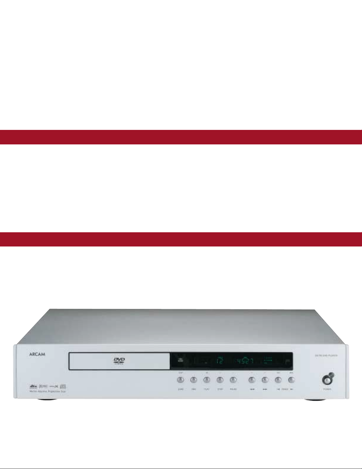
DiVA
DV78 DVD Player
Service
Manual
Issue 1.0
ARCAM
Bringing music & movies to life

DV78
Contents List
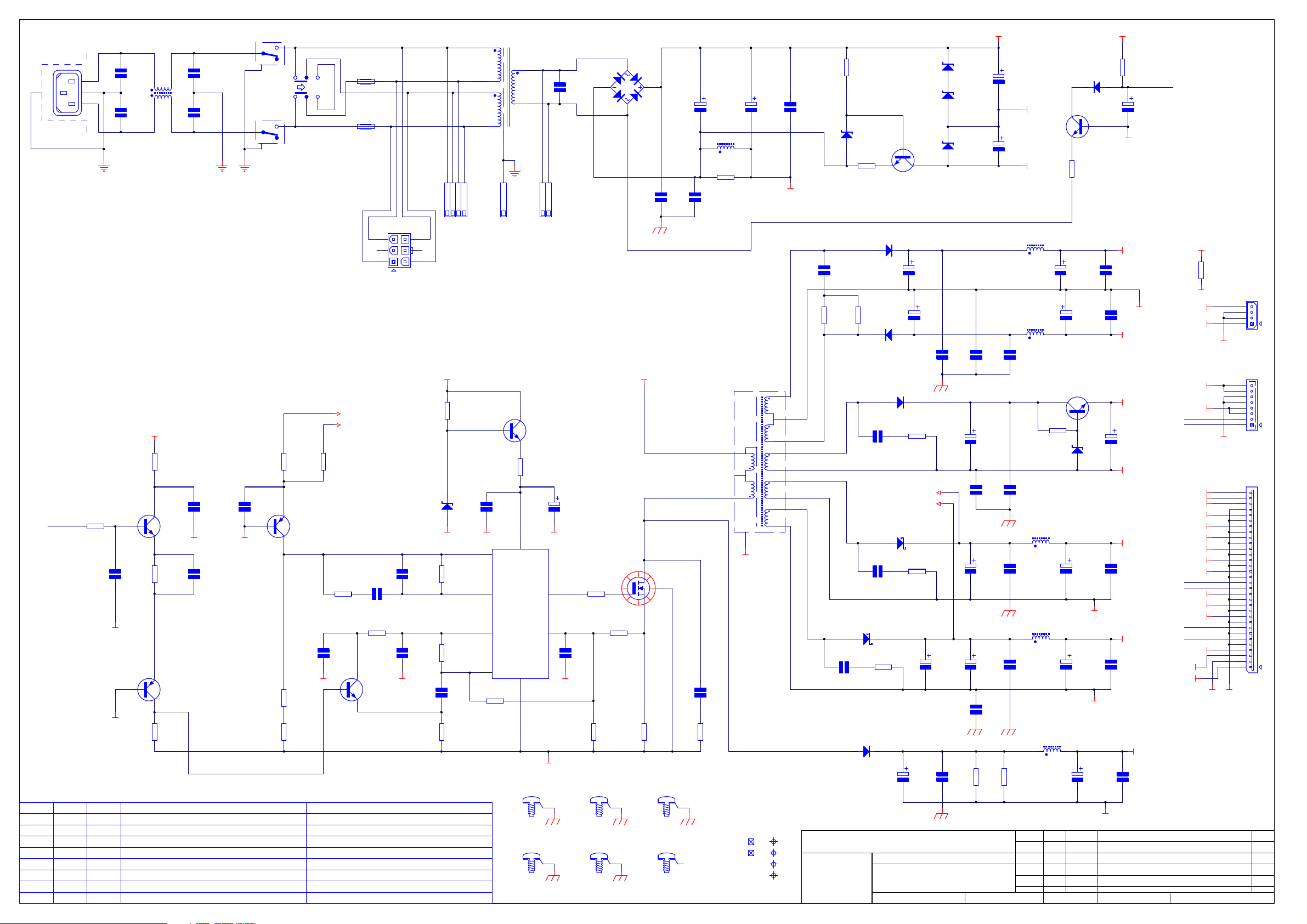
Circuit Description
Power Supply L959AY
! CCT diagram
! Component layout diagram
! Parts list
Main Board L960AY
! CCT diagram
! Component layout diagram
! Parts list
Display Board L961AY
! CCT diagram
! Component layout diagram
! Parts list
Transformers
! L924TX
! L925TX
Mechanical Assembly
! Exploded view diagram
! Mechanical and packing part list

Diva Dv78 circuit description
Overview
DiVa DV78
The
that share a similar circuit topology to the earlier
released Vaddis V based players such as the Diva
88+, Diva 89, DV27.
The player is based around acclaimed
V
chipset coupled to high specification Wolfson D to A
converters for Left and Right channels.
Power supply board.
Non-switching
Mains power arrives at IEC inlet socket SKT1 and is
filtered by EMC choke LI and Y caps C3 and C4,
mains switch SW2a/b switches both Negative and Live
phases before the power reaches the mains select
switch at location SW1 the switch allows the primary
windings of the transformer
Parallel or Series configuration.
The Bridge rectifying Diode package at location D1
forms the basis of the conventional power stage and
supplies a VN35V6 (-35.6v) to the Switch mode
stage, transistor
DZ1
and allows for the series Zener diodes DZ2, DZ3,
DZ3
to supply the VN13V5 and VN19V rails.
We will also see a simple
used for delayed output relay operation and fast relay
closure under interrupted supply conditions thus
preventing op-amp offsets from reaching the Audio
output sockets.
Switch mode
The switch mode supply is formed around the
Driver/Control
mode). The chip is referenced the –36.5V supply line
and the Digital ground DGND, the supply for the chip
is formed by the 12v Zener at location
seen on Pin 7 as VCC. The power supply allows for
the switch-mode to be tied the to Audio sampling
frequency for any given compatible format.
is a completely new design platform
Zoran Vaddis
TX1
to be wired in either
TR1
is biased by 2v7 Zener diode
A.C present circuit
IC1
chip
UC3843 (used in regulating
DZ6
this is
and can be
Fig 1 PSU clock control
Fs
Frequency
select
44.1 kHz 0 0 44.1 kHz
48 kHz 0 0 48 kHz
88.2 kHz 0 1 44.1kHz
96 kHz 0 1 48 kHz
176.4 kHz 1 0 44.1 kHz
192 kHz 1 0 48 kHz
Others 1 1 OFF
PSUFS1
Pin 11
IC305a
PSUFS0
Pin 12
IC305a
PSUCLK
Output Pin 5
of IC305a
The PSU sync signal is driven into the power supply via
Resistor R9 if no Sync is present the unit is set to free run x
due to the RT/RC network attached to Pin 4.
IC1
is running in regulated mode and monitors the voltage
output on the +5V and +3V3 D.C lines, the two voltages are
summed by
TR8
and Driven into the VFB and Comp inputs
of IC1, the Voltage is then regulated by changing the time
base of the PWM output at pin 6 (longer the time base the
lower the voltage), the
PWM switching frequency
into the switch-mode transformer by the high speed Nmos
device at position M1, R5 is used to sense the Current
across the gate of the Nmosfet and in the event of a short
circuit will safely shut the power supply down. We derive the
12v Mech supply from the output of M1 using the Ultra-fast
Diode at location D8 to rectify the PWM line.
The D.C outputs from the switch mode have extensive
switch mode noise removing filters these are seen as 100n
caps down to ground and Wire wound inductors in series
with the supply rail.
Power supply main board
All the power supply rails are supplied to the main board via
the 32 way FFC connector at location
CON1001
The Digital supplies from the switch mode stage of the
power supply arrive as 3V3D, +5VD and +12VD we also see
the Display board power supplies arrive as –19V, -9 and
–13.5V all of the supplies have a second stage of
implemented on the board to remove all traces of ultra-sonic
noise.
The 3V3D rail is the main 3V3 rail used to power the digital
circuitry; +5VD is used for all 5v Digital/Video supplies the
+12VD is used for Scart switching.
is driven
.

The 1V8 rail is derived from the 3V3 rail and is
regulated by the adjustable regulator at location
REG1003
The
as +15V3 and –15V3 rails these are filtered L1002 and
L1015 before being regulated by the adjustable
regulators at locations
provide +/- 12V rails for the Analogue output stage.
Regulator
forms the Audio DAC supply.
The Display board requires several supply voltages
these are simply passed through the main board,
being filtered on the way to prevent transmission of
noise through to the surrounding electronics. The
display takes the +5V, -19V, -13V5 and -9V the –13V5
and –9V form a floating 4.5V supply biased relative to
the –19V grid voltage.
Display Board
The main component of the Display board is
a Vacuum Florescent Display driver with keyboard san
and a serial data in/out interface.
The Chip receives display drive serial data from the
Vaddis V
13 and 14 these will be seen a DIN, STS and CLK this
data is used to drive the VFD a DOUT line interfaces
with the VADDIS V and supplies Keyboard Scan
information. The keyboard scan is a 6 x 4 matrix with
the Key Source appearing at S3, S4, S5, S6 and the
Keyscan
Please see:
The
data and send the data to the Vaddis V on the main
board via transistors TR2 and TR3, LED 2 is used to
mix the rear panel RC5.
The
RC5 code; this is filtered for ultra sonic noise by the
inductors at locations L900 and L901 and then passed
to the Infrared diode on the display at location LED2.
.
Analogue
Infra red
rear panel 3.5mm
supply stages arrive at the main board
REG1000
REG1001
chip on the main board via Con1 on pins 12,
data returns appearing a K2, K3 and K4.
above for
is fed from the +15V3 rail and
power supply
pick-up at location RXI receives RC5
input jack receives modulated
REG1002
and
information.
IC1
to
this is
Main Board electronics DV78.
Zoran Vaddis V.
The main processor/control chip on the main board is the
Zoran Vaddis V at location IC202, this is the latest
incarnation of the very popular Vaddis range of processors
and allows for a much lower component count when
compared to our earlier players as many of the playback
functions have moved onto the Vaddis V silicon.
Below you will see the
when used with the DV78.
Decoded Analogue Video output (internal
o
DAC) used on the DV78 only.
o SPDIF output.
o Internal display interface.
o Internal ATAPI interface.
o Internal IR interface.
o Serial in/out for RS232 (Optional).
A more detailed explanation of the Vaddis V and
peripheral components follows.
Vaddis Power
The Vaddis V is powered by two separate supplies the
Vaddis requires a 1.8v supply for the core, this is regulated
from the 3.3v rail by REG1003, the 3.3v rail is used to
supply power to the I/P – O/P ports of the chip.
ATAPI interface
CON203
connector. This is decoupled from the Drive via an array of
decoupling resistors as required by the ATAPI spec.
is an ATAPI interface on a 40 way IDE
major functions
of the Vaddis V
Display Board interface
The display board interface is on the 16 way FFC flexi
foil connector at location CON202. Power for the
display also travels on the connector. There are 4 –
wires to interface with the VFD driver chip these are
seen as.
XFPDIN - Data to the display board
o
o FPDOUT - Data from the display board
o XFPCLK - Clock
o XFPSEL - Chip select
The above control lines are level shifted to 5v logic
from 3.3v levels by
IC200
(74HCT125) these are the
levels required by the VFD drive chip.
The IR output from the Display board arrives as
IRRCV
this is an open collector signal, which can be
wire-Ord with the re-panel remote input.
Digital Audio
The Digital audio leaves the chip as 1 data line
labelled as.
o ADAT0 - Left and Right channel data
Along with the ADAT line we will also see the
ABCLK
and ALRCK as required for IS2 data conversion.
The Vaddis V also supplies a direct SPDIF output for
interfacing with ancillary processing equipment.
Flash/ SDRAM
IC203 is a 64Mbit (32 bit x 2Meg) SDRAM. It runs at
135MHz
IC205
is a 16Mbit (16 bit x 1Meg) intel type flash IC for
program storage (Player software).
The flash interfaces to the Vaddis V using the SDRAM
bus it may appear that the bus connects to the flash in
a random manner, however this is simply because the
Vaddis bus is multiplexed that way. The Flash will be
accessed at power up and the contents are copied to
the SDRAM the program will then be run from the
SDRAM.
Series resistors are employed to isolate the flash bus
from the main SDRAM bus.
EEPROM
IC204 is a 8kBit (1K x 8) Serial EEPROM. This is used
for storage of non-volatile storage of player settings,
region settings and bookmark data.
Clocks
CLK27MV
is the 27Mhz clock for video. It is used to
generate the 135Mhz clock for the Vaddis microprocessor
and DSP. The
MCLKV
is the audio master clock for the
Vaddis.
We run the Vaddis in
PLL bypass
mode and generate or
own master clock (see main clock section of manual) for
higher accuracy and improved performance across Audio
and Video.
RESET
IC201
is a reset generator chip that monitors the +3.3V rail
and ensures a reset signal
PWR_ON_RESET*
is
generated on power up, or if the mains power dips below
an operational level.
This signal is used to reset the Vaddis V and Flash micro
only. The Vaddis V line labelled as RESET* resets the
remaining circuitry of the player apart from the HDMI chip,
this has it’s own reset line labelled as HDMI_RESET this is
necessary if we require to reset the HDMI chip only (for
example when the HDMI sink is connected and then
disconnected).
Serial Port
The VADDIS V can interface with the external world via
the RS232 connector at location CON900 and the RS232
Transceiver at location IC900, the serial data lines are
shown as SERIAL RX and SERIAL TX these lines allow
for direct control over the unit via RS232.
Fig 2. GPIO control signals from the Vaddis V
Single Name I/P-O/P Function
PSUFSO-1 Output
ENABLE_AV Output
16/9 Output
GAIN_SCALING Output
ML_8740_0-2 Output
MC Output
MD Output
FSELE0-1 Output
MUTE* Output
RESET* Output
Control PSU Clock
divider
SCART control High
in normal operation
and low in standby
Scart 16/9
anamorphic control
line
High for HDCD gain
scaling
SPI load signal for
Audio DACs 0
SPI clock signal for
DAC control
SPI data signal for
DAC control
Frequency select
generator
Active low audio
mute signal
System reset

Clocks and SPDIF stage.
IC300
powered from the +5V(D) rail. The Chip runs in
software mode and is slaved from the Vaddis V (data
coming in on the MD line).
X300
all the video and audio clocks required by the system
the crystal sits on the XTI and XTO pins of the chip,
the 27Mhz output at Pin 10 (MCKO) is used to drive
the Vaddis chip directly bypassing the internal PLL.
The frequency of the audio master is dependent on
the on the current audio sample rate (I.e the sample
rate required by the format CD=44.1Khz and
DVD=48khz etc) and this is set by the system micro
via the MD, MC and ML_1700 lines from the Vaddis V.
Clock Buffer
IC301 us used to buffer the audio master clock. The
circuit is arranged so that each device that requires
the audio master clock has it’s own driver these are
seen as.
o MCLK_DAC0 - Pin 18
o MCLK_DAC1 – Pin 16
o
o MCLK_VADDIS – Pin 3
o MCLK_HDMI – Pin 9
We also run the
this can be seen on Pin 12 and drives transistor
TR401
RLY500, RLY600
outputs.
IS2 Audio Data
IC302
ensure that the signals travelling to the DAC’s are
point to point.
ABCLK
ADAT0,1,2 all signal are split into three separate lines
for the three stereo DACS.
PSU Clock Divider
IC304 a/b
the PSU clock is always either
fig 1
The circuit is fed from the
selected PSUCLK is controlled by
PSUFS1
The output of the PSU circuit can be seen to leave
IC305
control information.
PLL1700E
is a
27Mhz
is a
MCLK_DAC2 – Pin 14
, the transistor pulls the relays
IC309
and
C309(NF DV78)
and I
form a clock divide by 1, 2 or 4 to ensure
within the power supply description section).
.
on pin 5 via R311. Please see
clock generator IC the chip is
crystal that
Mute Line
to ground and un-mutes the audio
are buffers for the 12S signals these
IC302
deals with the
IC300
uses to generate
from the Vaddis V
RLY400,
ALRCK
the
44.1kHz
ALRCLK
or
(Audio clock) the
PSUFSO
Fig 1
IC301
and
48Khz (See
and
for PSU
The circuit will also switch the
between sample rates (the PSU will free run when the
PSUCLK is not present).
SPDIF Output
The SPDIF output consists of
inline buffer and parallel output buffer. Gate A buffers the
signal so that the SPDIF line from the VADDIS sees fewer
loads and form a feed to the Optical output transmitter,
gates B,C and D drive the SPDIF in parallel so that we can
drive a 75ohm load adequately. The resistors at the output
of IC901 are arrange so that the output will be
pk when the output is terminated with a 75 ohm load at the
same time the output impedance of the circuit is 75ohms
as required by the Sony Philips Digital Interface
specification.
Left and Right channel D to A stages
Wolfson WM8740
The
requires +5V(A) and a +3V3 supply along with the Digital
Audio data lines already described in this guide.
The Left channel output only will be described in this
section.
IC400B
Bessel filter with a differential input and a gain of 1 this
follow by a output buffer IC401B, the gain of IC401B is
control by the switching chip at location
use the Gain of IC401B is set to 1.1 but in
the
R413 and the gain is set to 2.2 allowing for the higher
audio output required by the HDCD standard.
C436 is an A.C coupling capacitor used to remove the few
mV of offset that the DAC produces; D400 provides
protection against from ESD.
The all
chip but will also mute the outputs instantly under mains
failure conditions. Switching drive is provided by TR401
(MUTE_BUF) and TR400 (AC_PRES) the relays are in
mute mode if either the input to TR401 is Low or if the
input to TR400 is high.
Please note:
outputs of the left/right audio stages.
and associated components form a 2nd order
IC402
switches a second 10k resistor in parele with
output relays
The
are under control of the Vaddis V
Scart
PSUCLK
IC901
stereo DAC ay location
left/right audio is fed from the
off when switching
implemented as a
500mV pk-
IC403
IC402
, in normal
HDCD
mode

Video Output stage
The DV78 video output stage makes use of the
VADDIS V’s on board video DAC stages and as such
does not use the superior Analogue devices video
encoder DV79/DV29 and is fed by the following video
lines from the Vaddis V.
Composite
o
o SVID_C
o SVID_Y
o V or Red
U or Blue
o
o Y or Green
If we look at the Composite stage only, we will see that
the Analogue video signal is filtered by C710, C711
and L705 before being passed through the Video Opamp at location
IC701
the output is decoupled by
capacitor C738 before reaching R714 this forms the
75 ohm load required. All other video outputs are
identical.
SCART Output
RGB and Composite video signals as well as Left and
right audio signals are all present on the SCART
output socket. As the RGB and YUV signals share the
same output port at the Vaddis V the player must be
set to RGB SCART operation to have a RGB output
on the SCART.
Please note
: When in RGB SCART mode the RGB
does not contain a Sync signal and the sync must be
taken from the Composite out (4 wire RGB).
Also present at the Scart are a number of control flags
for the monitor these include 2 GPIO control lines
direct from the Vaddis.
ENABLE_AV
o
o 16/9
These are seen at the SCART output pins as.
o O/6/12
o RGB STAT
The 0/6/12 line (SCART pin 8) is used to inform the
monitor of the screen format being sent by the player
as set in the video set-up section of the software.
Standby = 0V
o
o 16:9 aspect ratio = 6V
o 4:3 aspect ration = 12V
The RGB status line (SCART pin 16) will be seen as
0v = no RGB and >1v is RGB present.
SW2A
DGND
SDDFC30400
SW1
18-000-0019
SW2B
SDDFC30400
C49
22N
100V
MKS2
5V_NFB
3V3_NFB
R7
6K8
0W25
MF
R4
4K7 0W25
MF
C15
100N
100V
MKS2
FHLDR1
20mm HLDR
FS1 T315mA
S504
FHLDR2
20mm HLDR
FS2
T315mA
S504
CON1
3
2
1
MOLEX
44472
(NFB From PSU Outputs)
C50
22N 100V
MKS2
R10
1K0 0W25
MF
TR4
BC546B
TO-92
VN35V6
2A22B
115V 230V
1A11B
MA NS SUPPLY
FOR EXT. AUDIO
SUPPLY TX
R11
9K1
0W25
MF
TR8
BC556B
TO-92
VN35V6
R26
68R
0W25
MF
R27
2K7
0W25
MF
USED TO SECURE TRANSFORMER CABLES TO PCB NEAR CON1
6
5
4
C51
22N
100V
MKS2
C16
100N
100V
MKS2
GREY
BLACK
3
4
GREY
DK GREY
CON2
WAGO
256
NOTE TRANSFORMER TX1 IS MOUNTED ON
THE CHASSIS AND CONNECTED TO THE PSU
PCB BY CON2,3,4. TX1 IS SHOWN ABOVE FOR
CIRCUIT OPERATION
DGND
R12
10K
0W25
MF
R14
NF
R15
10K
0W25
MF
C56
4N7
100V
CER
R28
22R
0W25
MF
SKT1
BULGIN
SH1
PX0580
NF
EMC Shield
N
E
L
QTY DESCRIPTIONPART No. NOTESITEM
R9
1K0 0W 25
MF
PSU CLK
ITEM1 1 Clip For SW Profile HeatsinkF006
ITEM2 1 Sil Pad For TO-220 HS InsulatorF082
ITEM3 2 Fuseholder Cover For 20mm FuseholderF022
ITEM4 1 Blank PCB DV78 PSUL959PB
ITEM6 1 Cable Tie 100MM X 2.5MMF044
ITEM5 1 Earth Lead Assy 75MM8M101 SAFETY EARTH WIRE FROM IEC INLET SK1 TO METAL CHASSIS
ITEM7 2 Rivet CopperHP007S RIVETS TO SECURE IEC INLET TO PCB
C1 C3
NF
4
1
C2
NF
VP5V
C47
22P
100V
N150
DGND
DGND
R8
1K0
0W25
MF
TR3
BC546B
TO-92
R13
10K
0W25
MF
TR7
BC556B
TO-92
R25
100R
0W25
MF
3N3
250V
3
CER
L1
250U
2
C4
3N3
250V
CER
C14
100N
100V
MKS2
VN35V6
C48
1N0
100V
CER
WH TE
BLUE
2
1
BLUE
LT GREY
DZ6
BZX79C
12V
DO-35
1
115V
2
3
115V
4
C17
100N
100V
MKS2
VN35V6 VN35V6VN35V6
2
VFB
1
COMP
8
VREF
4
RT/CT
R29
82K 0W25
MF
TX1
Small Toroidal Mains
L924TX
7
1
GREEN
CON3
WAGO
256
7
VCC
GND
5
FIX1
Dia 3.5mm
FIX2
Dia 3.5mm
5
6
TR5
BD179
TO-126
R17
10R
0W25
MF
CON4
WAGO
256
OUT
ISEN
VN35V6
1
GREY2GREY
1
1
C40
220UF
16V
YXF
IC1
UC3843AN
DIP-8
6
3
VN35V6
C5
NF
33R 0W25
C52
330P
100V
N750
R24
MF
R16
47K
0W25
MF
FIX3
Dia 3.5mm
FIX4
Dia 3.5mm
HS1B
SW38-2
10 2C/W
R5
4K7 0W25
MF
1
1
D1
2KBP02
DGND
M1
IRF640N
TO-220
R30
0R22
3W
SPRX
FIX5
Dia 3.5mm
FIX6
Dia 3.5mm
C6
100N
100V
MKS2
1
1
C27
1000UF
63V
YK
L2
NF
LK1
0R0 0W 25 MF
C7
100N
100V
MKS2
TX2
Ferrite Switch Mode
L925TX
C36
1N0
100V
CER
R31
10R
0W25
MF
C28
1000UF
63V
YK
1 11
16T
2
16T
3
SCR
DGND
FD1
FD2
41T
41T
22T
14T
10T
VN35V6
4
5
6
12
9
10
7
8
TOOL1
TOOL2
TOOL3
TOOL4
C8
100N
100V
MKS2
C32
470pF
1kV
DE
R20
470R
0W25
MF
1N0 100V
DRAWING TITLE
A & R Cambridge Ltd.
Pembroke Avenue
Waterbeach
Cambridge CB5 9PB
R1
22K
0W25
MF
DZ1
BZX79C
2V7
DO 35
R2
220R
0W25
MF
D6
31DQ10 DO-201AD
C34
CER
D8
UF5406
DO-201AD
TR1
BC547B
TO-92
D2
UF4003
DO-41
R21
470R
0W25
D3
MF
UF4003
DO-41
D4
UF4003
DO-41
C33
1N0 100V
CER
NFB (To Controller E/A)
D7
31DQ06 DO-201AD
C35
1N0 100V
CER
R18
10R 0W25
MF
DV78 SERIES PSU
Filename:
Notes:
Contact Engineer:
C37
100UF
50V
YXF
C38
100UF
50V
YXF
R23
33R 0W25
MF
5V_NFB
3V3_NFB
R19
10R 0W25
MF
C57
470UF
25V
YXF
L959_1.1.sch
C53
1000UF
16V
YXF
C9
100N
100V
MKS2
C24
100N
100V
MKS2
DZ2
BZX79C
10V
DO 35
DZ3
BZX79C
3V3
DO 35
DZ4
BZX79C
5V6
DO 35
DGND
C29
22UF
63V
YK
VN13V5_F1
C30
22UF
63V
YK
VN19V
L3
33U 1.17A 8RHT2
L4
33U 1.17A 8RHT2
C10
100N
100V
MKS2
C39
220UF
16V
YXF
C18
100N
100V
MKS2
C54
1000UF
16V
YXF
C55
1000UF
16V
YXF
C25
100N
100V
MKS2
R32
NF
Contact Tel: (01223) 203200Kevin Lamb
C11
100N
100V
MKS2
470R 0W25
C19
100N
100V
MKS2
L6
6U8 2.1A 8RHT2
C20
100N
100V
MKS2
L7
6U8 2.1A 8RHT2
C21
100N
100V
MKS2
33U 1.17A 8RHT2
R33
1K0
0W25
MF
ECO No. DESCRIPTION OF CHANGE
L5
INITIALS
Printed:
R22
MF
R3
4K7
0W25
MF
C41
470UF
25V
YK
C42
470UF
25V
YK
C44
470UF
25V
YK
C45
470UF
25V
YK
DATE
22 Apr2004
D5
1N4148
DO 35
TR2
BC546B
TO-92
TR6
BD179
TO-126
DZ5
BZX79C
5V1
DO 35
DGND
DGND
C46
470UF
25V
YK
DGND
Make CON1 fitted (used in DV29)22/04/04PG04_E046
Production release02/07/03KAL03_E195
VP5V
C12
100N
100V
MKS2
DGND
C13
100N
100V
MKS2
C43
470UF
25V
YK
C22
100N
100V
MKS2
C23
100N
100V
MKS2
1 1Sheet of
R6
6K8
0W25
MF
C31
22UF
63V
YK
VP15V5
AGND
VN15V5
VN9V_F2
VN13V5_F1
VP5V
VP3V3
VP12V
C26
100N
100V
MKS2
AC_PRES*
AGND
DGND
VP5V
VP12V
VP5V
VP3V3
SPARE1
SPARE2
VN19V
VN9V_F2
VN13V5_F1
VP3V3
VP3V3
VP3V3
VP3V3
VP3V3
VP3V3
SPARE3
SPARE4
VP5V
VP5V
VP5V
PSU_CLK
AC_PRES*
VP12V
VP15V5
VN15V5
DRAWING NO.
LK2
NF
DGND
DGND
DGNDAGND
L959CT
CON5
4
3
2
1
Amp
HD Pwr Con
CON6
8
7
6
5
4
3
2
1
AMP
CT
NF
CON7
32
31
30
29
28
27
26
25
24
23
22
21
20
19
18
17
16
15
14
13
12
11
10
9
8
7
6
5
4
3
2
1
MOLEX
52045
1.1
1.0
ISSUE
DV78 DVD player PSU board L959AY issue 1.1.1
Designator Part Description
C1 2J410 Capacitor SM 0805 X7R Ceramic 10% 50V 100N
C2 2J410 Capacitor SM 0805 X7R Ceramic 10% 50V 100N
C3 2J410 Capacitor SM 0805 X7R Ceramic 10% 50V 100N
C4 2J410 Capacitor SM 0805 X7R Ceramic 10% 50V 100N
C5 2MA610 Capacitor Surface Mount Electrolytic 10UF 50V 6.3 X 4.5MM
C6 2MA610 Capacitor Surface Mount Electrolytic 10UF 50V 6.3 X 4.5MM
C7 2MA610 Capacitor Surface Mount Electrolytic 10UF 50V 6.3 X 4.5MM
C8 2L210 Capacitor SM 0805 NPO Ceramic 5% 100V 1N0
C9 2L210 Capacitor SM 0805 NPO Ceramic 5% 100V 1N0
C10 2L210 Capacitor SM 0805 NPO Ceramic 5% 100V 1N0
C11 2L210 Capacitor SM 0805 NPO Ceramic 5% 100V 1N0
CON1 8K8616 Con 1.0MM Horiz FFC 16WAY 52807 Series
D1 3AS16W Diode Surface Mount Small Signal BAS16W SOT-23 Package
D2 3AS16W Diode Surface Mount Small Signal BAS16W SOT-23 Package
D3 3AS16W Diode Surface Mount Small Signal BAS16W SOT-23 Package
D4 3AS16W Diode Surface Mount Small Signal BAS16W SOT-23 Package
DISP1 B1014 Display DV88
IC1 5H6312 IC VFD Driver PT6312LQ SM LQFP-44 package
LED1 3D007 LED 3.1mm Green SLR-37MG3T
LED2 3D010 LED SM Red SML-010LT
LED3 3D007 LED 3.1mm Green SLR-37MG3T
LED5 3D006 LED 3mm Red/Green Tri-Colour L-93WEGW
R1 1M133 Resistor 0805 Surface Mount 0.125W 1% 330R
R2 1M133 Resistor 0805 Surface Mount 0.125W 1% 330R
R3 1M133 Resistor 0805 Surface Mount 0.125W 1% 330R
R4 1M122 Resistor 0805 Surface Mount 0.125W 1% 220R
R5 1M118 Resistor 0805 Surface Mount 0.125W 1% 180R
R6 1M139 Resistor 0805 Surface Mount 0.125W 1% 390R
R8 1M310 Resistor 0805 Surface Mount 0.125W 1% 10K
R9 1M310 Resistor 0805 Surface Mount 0.125W 1% 10K
R10 1M247 Resistor 0805 Surface Mount 0.125W 1% 4K7
R11 1M356 Resistor 0805 Surface Mount 0.125W 1% 56K
R13 1M310 Resistor 0805 Surface Mount 0.125W 1% 10K
R14 1M310 Resistor 0805 Surface Mount 0.125W 1% 10K
R15 1M310 Resistor 0805 Surface Mount 0.125W 1% 10K
RX1 B2109 IR Receiver Module Kodenshi KSM-902TM1N
SW1 A1511 Switch Tact Low Profile No Gnd Pin
SW2 A1511 Switch Tact Low Profile No Gnd Pin
SW3 A1511 Switch Tact Low Profile No Gnd Pin
SW4 A1511 Switch Tact Low Profile No Gnd Pin
SW5 A1511 Switch Tact Low Profile No Gnd Pin
SW6 A1511 Switch Tact Low Profile No Gnd Pin
SW7 A1511 Switch Tact Low Profile No Gnd Pin
SW8 A1511 Switch Tact Low Profile No Gnd Pin
SW9 A1511 Switch Tact Low Profile No Gnd Pin
TR2 4D10KN Digital Transistor MMUN2211LT1 SOT23 Package
TR3 4A849B Transistor BC849B SOT23 Package
TR4 4A849B Transistor BC849B SOT23 Package
TR5 4D10KP Digital Transistor MMUN2111LT1 SOT23 Package
DRIVE
CON100
1
2
3
4
5
6
7
8
9
10
11
12
13
14
15
16
17
18
19
20
21
22
23
24
25
26
27
28
29
30
31
32
33
34
35
36
37
38
39
40
3M
2540
DISPLAY
CON101
1
2
3
4
5
6
7
8
9
10
11
12
13
14
15
16
MOLEX
52806
POWER IN
CON102
1
2
3
4
5
6
7
8
9
10
11
12
13
14
15
16
17
18
19
20
21
22
23
24
25
26
27
28
29
30
31
32
MOLEX
52045
DGND DGND
DGND
FPDOUT
XFPCLK
XFPSEL
XFPDIN
REMOTE_BUS_P
IRRCV
+5V_DISPLAY
-19V_OUT
-13V5_OUT
-9V_OUT
DGND
-19V_IN
-9V_ N
-13V5_ N
+3V3D_ N
Spare
Spare
XATRESET*
ATDD7
ATDD8
ATDD6
ATDD9
ATDD5
ATDD10
ATDD4
ATDD11
ATDD3
ATDD12
ATDD2
ATDD13
ATDD1
ATDD14
ATDD0
ATDD15
ATDMARQ
ATDIOW*
ATDIOR*
ATIORDY
ATDMACK*
AT NTRQ
ATDA1
ATDA0
ATDA2
ATCS0*
ATCS1*
+5VD_IN
PSUCLK
AC PRES*
+12VD_ N
+15V5_ N
-15V5_ N
ATDD[0..15]
REMOTE_BUS_N
L960C10_1.2.Sch
L960C2_1.2.sch
ATDD[0..15]
XATRESET*
VADDIS V
SHEET 2
ATDMARQ
ATDIOW*
ATDIOR*
ATIORDY
ATDMACK*
ATINTRQ
ATDA1
ATDA0
ATDA2
ATCS0*
ATCS1*
FPDOUT
XFPCLK
XFPSEL
XFPD N
IRRCV
-19V_IN
-9V_ N -13V5_OUT
-13V5_ N
+3V3D_ N
ADAT_DAC0
ADAT_DAC1
ADAT_DAC2
CLK27M_VADDIS
MCLK_VADDIS
ML_8740_0
GA N_SCAL NG
ML_8740_1
ML_8740_2
COMPOSITE
ENABLE_AV
SERIAL_RX
SERIAL_TX
-9V_OUT
-19V_OUT
+5V_DISPLAY
POWER
SHEET 10
+5VD_ N
+12VD_ N
+15V5_ N
-15V5_ N
RESET*
ML_1700
PSUFS0
PSUFS1
ABCLK
ALRCLK
MUTE*
Y/GREEN
U/BLUE
V/RED
SVID_Y
SVID_C
16/9
SPDIF
ANALOGUE AUDIO OUTPUTS
RESET*
MD
MC
MD
MC
ML_1700
PSUFS0
PSUFS1
ADAT_DAC0
ADAT_DAC1
ADAT DAC2
ABCLK
ALRCLK
MUTE*
L960C3_1.2.Sch
RESET*
MD
MC
ML_1700
PSUFS0
PSUFS1
ABCLK
ALRCLK
MUTE*
ABCLK_DAC0
ALRCLK_DAC0
MCLK_DAC0
MUTE_BUF*
ADAT_DAC0
ABCLK_DAC0
ALRCLK_DAC0
MCLK_DAC0
MD
MC
RESET*
MUTE_BUF*
L960C4_1.2.Sch
ADAT_DAC0
ABCLK_DAC0
ALRCLK_DAC0
MCLK_DAC0
MD
MC
ML_8740_0
RESET*
GAIN_SCAL NG
MUTE_BUF*
AC_PRES*
DAC L&R
LEFT_OUT
LEFT_OUT_GND
RIGHT_OUT
RIGHT_OUT_GND
SCART_LEFT
SCART_RIGHT
LEFT_OUT
LEFT_OUT_GND
RIGHT_OUT
RIGHT_OUT_GND
SKT100
KUNMING
GOLD
LEFT
RIGHT
SHEET 4
CLK27M_VADDIS
MCLK_VADDIS
ML_8740_0
GAIN_SCAL NG
ML_8740_1
ML_8740_2
Y/GREEN
U/BLUE
V/RED
SVID_Y
SVID_C
COMPOSITE
ENABLE_AV
16/9
CLK27M_VADDIS
MCLK_VADDIS
CLOCKS
SHEET 3
ABCLK_DAC1
ALRCLK_DAC1
MCLK_DAC1
ABCLK_DAC2
ALRCLK_DAC2
MCLK_DAC2
PSUCLK
ADAT_DAC1
ABCLK_DAC1
ALRCLK_DAC1
MCLK_DAC1
MD
MC
RESET*
ADAT DAC2
ABCLK_DAC2
ALRCLK_DAC2
MCLK_DAC2
MD
MC
RESET*
L960C5_1.2.Sch
ADAT_DAC1
ABCLK_DAC1
ALRCLK_DAC1
MCLK_DAC1
MD
MC
ML_8740_1
RESET*
LS_OUT
LS_OUT_GND
RS_OUT
RS_OUT_GND
DAC LS&RS
SHEET 5
L960C6_1.2.Sch
ADAT_DAC2
ABCLK_DAC2
ALRCLK_DAC2
MCLK_DAC2
MD
MC
ML_8740_2
RESET*
CENTRE_OUT
CENTRE_OUT_GND
SUB_OUT
SUB_OUT_GND
DAC CENTRE&SUB
LS_OUT
LS_OUT_GND
RS_OUT
RS_OUT_GND
CENTRE_OUT
CENTRE_OUT_GND
SUB_OUT
SUB_OUT_GND
SKT101
LEFT SURROUND
RIGHT SURROUND
KUNMING
(NOT FITTED)
GOLD
NF
SKT102
CENTRE
SUB
KUNMING
(NOT FITTED)
GOLD
NF
SH100
EMC Shield
SHEET 6
VIDEO OUTPUTS
SPDIF
Y/GREEN
U/BLUE
V/RED
SVID_Y
SVID_C
COMPOSITE
L960C7_1.2.Sch
COMPOSITE_OUT
Y/GREEN
COMPOSITE_OUT_GND
U/BLUE
V/RED
SVID_Y
SVID_C
COMPOSITE
SVID_C_OUT_GND
SVID_Y_OUT_GND
VIDEO FILTERS
SHEET 7
SCART_COMPOSITE
Y_OUT
Y_OUT_GND
V_OUT
V_OUT_GND
U_OUT
U_OUT_GND
SVID_C_OUT
SVID_Y_OUT
SVID_SCRN
SCART_GREEN
SCART_BLUE
SCART_RED
Y_OUT
Y_OUT_GND
V_OUT
V_OUT_GND
COMPOSITE_OUT
COMPOSITE_OUT_GND
U_OUT
U_OUT_GND
SVID_C_OUT_GND
SVID_C_OUT
SVID_Y_OUT
SVID_Y_OUT_GND
SVID_SCRN
SCART_GREEN
SCART_BLUE
SCART_RED
SCART_COMPOSITE
SCART_LEFT
SCART_RIGHT
SKT103
KUNMING
GOLD
SKT104
KUNMING
GOLD
L960C8_1 2.Sch
SCART_LEFT
SCART_RIGHT
SCART_GREEN
SCART_BLUE
SCART_RED
SCART_COMPOSITE
ENABLE_AV
16/9
SCART
COMPONENT - Y
COMPONENT - Cr
COMPOSITE
COMPONENT - Cb
Y C
SKT105
GNDY
SCRN1
HOSIDEN
TCS
GNDC
SCRN2
S-VIDEO
SHEET 8
REMOTE BUS
SKT106
KUNMING
HTJ
NC
SPDIF
SERIAL_TX
SERIAL_RX
ENABLE_AV
REMOTE_BUS
REMOTE_BUS_GND
L960C9_1.2.Sch
SPDIF
SERIAL_TX
SERIAL_RX
ENABLE_AV
REMOTE_BUS
REMOTE_GND
SPDIF & COMMS
SHEET 9
IRRCV
REMOTE_BUS_P
REMOTE_BUS_N
SPDIF_OUT
SPDIF_GND
IRRCV
SPDIF_OUT
SPDIF_GND
SKT107
KUNMING
GOLD
DIGITAL AUDIO OUT
SCRN
EMC_GND
ITEM100 1 Blank PCB DV78 DVD Player Main BoardL960PB
DRAWING TITLE
A & R Cambridge Ltd.
Pembroke Avenue
Waterbeach
Cambridge CB5 9QR
DV78 MAIN BOARD TOP LEVEL
Filename:
Notes:
Contact Engineer:
L960C1_1.2.Prj
03_E322 PG 02-12-03 Component value changes to digital output 1 2
03_E214 PG 16-07-03 Change damping pads from Sorbothane to rubber 1.1
03_E200 PG 03-07-03 Production Release 1.0
Contact Tel: (01223) 203270Peter Gaggs
ECO No. DESCRIPTION OF CHANGE
INITIALS
Printed:
DATE
2 Dec 2003
1 10Sheet of
EMC_GND
A2
1
DRAWING NO.
ISSUE
L960C1
Place these close to SDRAM
SDRAM DECOUPL NG
+3V3D
C212
C213
C214
100N
100N
16V
16V
0603
0603
RAMDAT5
RP200A
RAMDAT6
RP200B
RAMDAT11 FRAMDAT11
RP200C
RAMDAT10 FRAMDAT10
RP200D
RAMDAT9
RP201A
RAMDAT8
RP201B
RAMADD9
RP201C
RAMADD8
RP201D
RAMADD7
RP202A
RAMADD6
RP202B
RAMADD5
RP202C
RAMADD4 FRAMADD4
RP202D
RAMADD3 FRAMADD3
RP203A
RAMDAT31
RP203B
RAMDAT30
RP203C
RAMDAT29
RP203D
RAMDAT28
RP204A
RAMDAT27
RP204B
RAMDAT26
RP204C
RAMDAT25
RP204D
RAMDAT24
RP205A
RAMDAT7
RP205B
RAMBA0
RP205C
RAMBA1
RP205D
RAMADD10
RP206A
RAMADD0
RP206B
RAMADD1
RP206C
RAMADD2 FRAMADD2
RP206D
RAMDAT16
RP207A
RAMDAT17
RP207B
RAMDAT18
RP207C
RAMDAT19
RP207D
RAMDAT20
RP208A
RAMDAT21
RP208B
RAMDAT22
RP208C
RAMDAT23
RP208D
PR252
RAMADD11
RAMDAT3 NF (32Mb+)
RAMDAT4 NF(AMD 16Mb)
RAMDAT12 NF (Intel 64Mb)
0W125 0805
0W125 0805
PNVMRB* NF(AMD)
PF243
0W125 0805
0W125 0805
0W125 0805
0W125 0805
Use these resistors o confgure for
ntel/AMD 8Mbit 16Mbit 32Mbit or
64Mbit devices
ntel 16Mb t is standard
address
DGND
100N
16V
0603
data
PR253
1 8
2 7
1 8
2 7
1 8
2 7
1 8
2 7
1 8
2 7
1 8
2 7
1 8
2 7
1 8
2 7
1 8
2 7
R206
56R
R207
56R
R252
56R
R208
56R
R253
56R
R209
56R
L200 120R@100MHz
VDD_DAC
+3V3D
1
3
9
15
29
35
VDD
VDD
IC203
SDRAM
VSS
VSS
72
86
+3V3D
R210
56R
0W125
0805
R222
0R0
0W125
0805
41
49
55
75
81
VDDQ
VDDQ
VDDQ
VDDQ
VDDQ
VDDQ
VDDQ
VDDQ
DQ0
DQ1
DQ2
DQ3
DQ4
DQ5
DQ6
DQ7
DQ8
DQ9
DQ10
DQ11
DQ12
DQ13
DQ14
DQ15
DQ16
DQ17
DQ18
DQ19
DQ20
DQ21
DQ22
DQ23
DQ24
DQ25
DQ26
DQ27
DQ28
DQ29
DQ30
DQ31
VSSQ
VSSQ
VSSQ
VSSQ
VSSQ
VSSQ
VSSQ
VSSQ
6
12
32
38
46
52
78
84
PF200
PF201
PF202
PF203
PF204
PF205
PF206
PF207
PF208
PF209
PF210
PF211
PF212
PF213
PF214
PF215
PF228
PF229
PF230
PF231
PF232
PF233
PF234
PF235
PF236
PF237
PF238
43
VDD
VDD
R225
1K0
0W063
0603
NF
C217
100N
16V
0603
NF
DGND
C215
100N
16V
0603
56R
FRAMDAT5
56R
FRAMDAT6
56R
63
56R
54
56R
FRAMDAT9
56R
FRAMDAT8
56R
63
FRAMADD9
56R
54
FRAMADD8
56R
FRAMADD7
56R
FRAMADD6
56R
63
FRAMADD5
56R
54
56R
56R
FRAMDAT31
56R
63
FRAMDAT30
56R
54
FRAMDAT29
56R
FRAMDAT28
56R
FRAMDAT27
56R
63
FRAMDAT26
56R
54
FRAMDAT25
56R
FRAMDAT24
56R
FRAMDAT7
56R
63
FRAMBA0
56R
54
FRAMBA1
56R
FRAMADD10
56R
FRAMADD0
56R
63
FRAMADD1
56R
54
56R
FRAMDAT16
56R
FRAMDAT17
56R
63
FRAMDAT18
56R
54
FRAMDAT19
56R
FRAMDAT20
56R
FRAMDAT21
56R
63
FRAMDAT22
56R
54
FRAMDAT23
FRAMADD11
FLASHA19
FRAMDAT3
FLASHA21
PR200
PR201
PR202
PR203
PR204
PR205
PR206
PR207
PR208
PR209
PR210
PR211
PR212
PR213
PR214
PR215
PR216
PR217
PR218
PR219
address data
RAMCKE
PCLK
RAMBA0
RAMBA1
RAMWE*
RAMCAS*
RAMRAS*
RAMCS*
RAMADD10
RAMADD9
RAMADD8
RAMADD7
RAMADD6
RAMADD5
RAMADD4
RAMADD3
RAMADD2
RAMADD1
RAMADD0
RAMDQM
67
CKE
68
CLK
22
BA0
23
BA1
17
WE
18
CAS
19
RAS
20
CS
24
A10/AP
66
A9
65
A8
64
A7
63
A6
62
C MEM SDRAM 512KX32BTX4 7NS
A5
61
A4
60
A3
27
A2
26
A1
25
A0
16
DQM0
71
DQM1
28
DQM2
59
DQM3
VSS
VSS
44
58
DGND
R200
VIDEO DAC REFERENCE VOLTAGE
4K7
0W125
0805
REF200
LM4041CEM3 ADJ
SOT23
DGND
2
RAMDAT0
RAMDAT1
RAMDAT2
RAMDAT3
RAMDAT4
RAMDAT5
RAMDAT6
RAMDAT7
RAMDAT8
RAMDAT9
RAMDAT10
RAMDAT11
RAMDAT12
RAMDAT13
RAMDAT14
RAMDAT15
RAMDAT16
RAMDAT17
RAMDAT18
RAMDAT19
RAMDAT20
RAMDAT21
RAMDAT22
RAMDAT23
RAMDAT24
RAMDAT25
RAMDAT26
RAMDAT27
RAMDAT28
RAMDAT29
RAMDAT30
RAMDAT31
+3V3D
DGND
PR220
PR221
PR222
PR223
PR224
PR225
PR226
PR227
PR228
PR229
PR230
PR231
PR232
PR233
PR234
PR235
PR236
PR237
PR238
PR239
PR240
PR241
PR242
PR243
PR244
PR245
PR246
PR247
PR248
PR249
PR250
PR251
FRAMADD5
FRAMADD6
FRAMADD7
FRAMADD8
FRAMADD9
FRAMADD11
FRAMDAT8
FRAMDAT9
FRAMDAT5
FRAMDAT6
FRAMDAT7
FRAMBA0
FRAMBA1
FRAMADD10
FRAMADD0
FRAMADD1
FRAMADD2
FRAMDAT10
FRAMDAT11RAMDAT4
FLASHA19
FRAMDAT3
FLASHA21
RESET*
FRAMADD4
PNVMCE*
FRAMADD3
FLASH DECOUPLNG
C220
100N
16V
0603
4
5
7
8
10
11
13
74
76
77
79
80
82
83
85
31
33
34
36
37
39
40
42
45
47
48
50
51
53
54
56
25
24
23
22
21
20
19
18
8
7
6
5
4
3
2
1
48
17
16
15
10
9
12
11
14
26
28
13
P280
ATDMARQ
ATDIOW*
ATDIOR*
ATIORDY
ATDMACK*
ATINTRQ
ATDA0
ATDA1
ATDA2
ATCS0*
ATCS1*
XATRESET*
A0
A1
A2
A3
A4
A5
A6
A7
A8
A9
A10
A11
A12
A13
A14
A15
A16
A17
A18
A19
A20
A21
RP
WE
WP
CE
OE
VPP
P236
R201
10K
0W125
0805
R205
56R
0W125
0805
ATDD[0 15]
+3V3D
37
VCC
IC205
FLASH
TE28F160
L936SW
TSOP48
GND
GND
46
27
DGND
47
VCCQ
VREF
C206
100N
16V
0603
ATAPI
DQ0
DQ1
DQ2
DQ3
DQ4
DQ5
DQ6
DQ7
DQ8
DQ9
DQ10
DQ11
DQ12
DQ13
DQ14
DQ15
ATDD[0 15]
29
31
33
35
38
40
42
44
30
32
34
36
39
41
43
45
1 24V
FRAMDAT31
FRAMDAT29
FRAMDAT27
FRAMDAT25
FRAMDAT23
FRAMDAT21
FRAMDAT19
FRAMDAT17
FRAMDAT30
FRAMDAT28
FRAMDAT26
FRAMDAT24
FRAMDAT22
FRAMDAT20
FRAMDAT18
FRAMDAT16
XATRESET*
ATDD0
ATDD1
ATDD2
ATDD3
ATDD4
ATDD5
ATDD6
ATDD7
ATDD8
ATDD9
ATDD10
ATDD11
ATDD12
ATDD13
ATDD14
ATDD15
ATDMARQ
ATDOW*
ATDOR*
ATIORDY
ATDMACK*
ATINTRQ
ATDA0
ATDA1
ATDA2
ATCS0*
ATCS1*
PF216
PF217
PF218
PF219
PF220
PF221
PF222
PF223
PF224
PF225
PF226
PF227
PF239
PF240
PF241
PF242
RP209D
RP209C
RP209B
RP209A
RP210D
RP210C
RP210B
RP210A
RP211A
RP211B
RP211C
RP211D
RP212A
RP212B
RP212C
RP212D
R238 82R 0805
R241 22R 0805
R242 22R 0805
R239 82R 0805
R243 22R 0805
R240 82R 0805
R244 33R 0805
R245 33R 0805
R246 33R 0805
R247 33R 0805
R248 33R 0805
R249 33R 0805
RESET
+3V3D
C207
VCC
100N
16V
GND
0603
DGND
PCLK
RAMCKE
RAMWE*
RAMCAS*
RAMRAS*
RAMCS*
RAMDQM
+5VD
R226
R227
1K0
0W125
0805
33R
33R
33R
33R
33R
33R
33R
33R
33R
33R
33R
33R
33R
33R
33R
33R
CLK27M VADDIS
DGND
R228
1K0
0W125
0805
R250
5K6
0W125
0805
2 7
1 8
2 7
1 8
1 8
2 7
1 8
2 7
1K0
0W125
0805
54
63
54
63
63
54
63
54
CLOCKS
Audio master clock (input)
Can be configured as an output or testing
MCLK VADDIS
To enab e Vaddis PLL for es ing:
Make PLLCFGA low
soate AMCLK rom GCLKA
Link GCLKA to GCLKP
Connect AMCLK_OUT to AMCLK
AMCLK is now an output and the Vaddis PLL is
enabled
P274
MCLK_VADDS
AMCLK OUT
IC201
RST
LM809M3 2 63
SOT23
R223
0R0
0W125
0805
NF
P239
RESET*
P243
P244
P245
P246
P247
P248
P249
P250
P251
P252
P253
P254
P255
P256
P257
P258
P259
P260
P261
P262
P263
P264
P265
P266
P267
P268
P269
P270
ATRESET*
+3V3D
Pn A9 used by S/W to
detect DV78
CLK27M_VADDIS
R219
0R0
0W125
0805
NF
R224
0R0
0W125
0805
RESET*
RAMBA1
RAMBA0
RAMADD11
RAMADD10
RAMADD9
RAMADD8
RAMADD7
RAMADD6
RAMADD5
RAMADD4
RAMADD3
RAMADD2
RAMADD1
RAMADD0
RAMDAT0
RAMDAT1
RAMDAT2
RAMDAT3
RAMDAT4
RAMDAT5
RAMDAT6
RAMDAT7
RAMDAT8
RAMDAT9
RAMDAT10
RAMDAT11
RAMDAT12
RAMDAT13
RAMDAT14
RAMDAT15
RAMDAT16
RAMDAT17
RAMDAT18
RAMDAT19
RAMDAT20
RAMDAT21
RAMDAT22
RAMDAT23
RAMDAT24
RAMDAT25
RAMDAT26
RAMDAT27
RAMDAT28
RAMDAT29
RAMDAT30
RAMDAT31
PNVMCE*
PNVMR/B*
P275
+3V3D
DGND
+1V8D
DGND
DGND
DGND
RESET*
C253
100UF
10V
YXF
C254
100UF
10V
YXF
+3V3D
NVMDA0
NVMDA1
NVMDA2
NVMDA3
NVMDA4
NVMDA5
NVMDA6
NVMDA7
NVMR/B
NVMCE
NVMR/B1
NVMCE1
NVMRE
NVMWP
NVMWE
NVMALE
NVMCLE
NVMCD
PCLK
RAMCKE
RAMWE
RAMCAS
RAMRAS
RAMCS
RAMDQM
RAMBA1
RAMBA0
RAMADD11
RAMADD10
RAMADD9
RAMADD8
RAMADD7
RAMADD6
RAMADD5
RAMADD4
RAMADD3
RAMADD2
RAMADD1
RAMADD0
RAMDAT0
RAMDAT1
RAMDAT2
RAMDAT3
RAMDAT4
RAMDAT5
RAMDAT6
RAMDAT7
RAMDAT8
RAMDAT9
RAMDAT10
RAMDAT11
RAMDAT12
RAMDAT13
RAMDAT14
RAMDAT15
RAMDAT16
RAMDAT17
RAMDAT18
RAMDAT19
RAMDAT20
RAMDAT21
RAMDAT22
RAMDAT23
RAMDAT24
RAMDAT25
RAMDAT26
RAMDAT27
RAMDAT28
RAMDAT29
RAMDAT30
RAMDAT31
PNVMCE
PNVMR/B
ATDD0
ATDD1
ATDD2
ATDD3
ATDD4
ATDD5
ATDD6
ATDD7
ATDD8
ATDD9
ATDD10
ATDD11
ATDD12
ATDD13
ATDD14
ATDD15
ATDMARQ
ATIOW
ATIOR
ATIORDY
ATDMACK
ATINTRQ
ATDA0
ATDA1
ATDA2
ATCS0
ATCS1
HD0
HD1
HD2
HD3
HD4
HD5
HD6
HD7
HA0
HA1
HA2
HA3
HWR
HRD
HCS
HIRQ
HACK
HCS1
HIRQ1
HACK1
XO
GCLKP
GCLKA
RESET
NF
DGND
C222
100N
16V
0603
H5
VDDPE5VDDPF5VDDP
VDDPK5VDDPN5VDDPR5VDDPE7VDDPT7VDDPU7VDDPT9VDDP
GNDPT5GNDPT6GNDPT8GNDP
GNDP
GNDP
GNDP
GNDP
GNDP
GNDP
T10
T12
T13
T14
T16
V13
U15
C223
C225
100N
100N
16V
16V
0603
0603
C224
C226
100N
100N
16V
16V
0603
0603
VADDIS DECOUPLNG
N3
P4
P3
R3
R4
P1
P2
N4
N1
L4
M3
L3
M1
N2
M2
L1
L2
M4
U12
V11
Y14
W13
Y13
Y12
W14
Y11
W11
U10
W9
V10
U9
V9
U8
V8
W7
Y7
Y8
W8
Y9
W18
Y18
W17
Y17
W16
Y16
W15
Y15
V14
U14
V15
V16
V17
U17
V18
U18
W6
Y6
W5
Y5
W4
Y4
Y3
Y2
W2
W3
V4
U4
V5
V6
U6
V7
Y1
W1
D2
C2
A1
B2
D3
C3
D4
C4
A4
B4
A3
B3
A2
E4
E3
F4
B1
C1
D1
F3
E2
E1
G3
F1
F2
G1
G2
B7
A7
B8
A8
B9
A9
B10
A10
B5
A5
B6
A6
C6
D6
D7
C7
C5
D8
C8
D5
C14
A14
B15
B14
C252
100UF
10V
YXF
C221
100N
16V
0603
K16
E10
T11
U11
E12
U13
E15
T15
VDDP
VDDP
VDDP
VDDP
VDDP
VDDP
VDDP
ZORAN VADDIS V
IC202
ZR36750
BGA-316
HS202
3319B+T410 01
209C/W
GNDPJ9GNDPK9GNDPL9GNDPM9GNDP
GNDP
GNDP
GNDP
GNDP
J11
J12
L10
K11
K12
C229
C227
100N
100N
16V
16V
0603
0603
C228
C230
100N
100N
16V
16V
0603
0603
+1V8D
M16
R16
U16
E13
L17
V12
W10
L5
D12
U5
VDDP
VDDP
VDDP
VDDP-A
VDDP-A
GNDP
GNDP
GNDC
GNDP
GNDP
GNDP
GNDP
GNDP
E8
J10
L11
L12
K10
M10
M11
M12
C232
C231
100N
100N
16V
16V
0603
0603
A18
E9
VDDC
GNDC
E14
A19
VDDC
VDDC
VDDC
VDDC
VDDC
VDD_DAC
GNDC
GNDC
GNDC
GNDCM5GNDA
GNDA
L16
Y10
A12
A11
W12
C234
C233
100N
100N
16V
16V
0603
0603
VDDP_A
VDD_DAC
VDD_PLL
C208
C248
100N
10UF
16V
50V
0603
GNDDAC-SB
A16
VDDADC
C236
100N
16V
0603
DAC D CVBS
GNDDAC-D
GNDDAC-D
B20
C20
DGND
DAC A B/U
DAC B R/V
DAC C G/Y
DAC E Y
DAC F C
COSYNC
VIDO 0
VIDO 1
VIDO 2
VIDO 3
VIDO 4
VIDO 5
VIDO 6
VIDO 7
VSYNC
HSYNC
VCLK
VCLKx2
VIDI 0
VIDI 1
VIDI 2
VIDI 3
VIDI 4
VIDI 5
VIDI 6
VIDI 7
V DI VS
V DI HS
VIDI CLK
VIDI VALID
AMCLK
ALRCLKI
ABCLKI
ALRCLKO
ABCLKO
AOUT0
AOUT1
AOUT2
AOUT3
AOUT4
SPDIF
FPCDOUT
FPCDIN
FPCCLK
FPCSTB
IRRCV
MODRI
MODDCD
MODDSR
MODCTS
MODDTR
MODRTS
MODRD
MODTD
DUPRD
DUPTD
SPIDATI
SPIDATO
SPICLK
I2CDAT
I2CCLK
SERADC0
SERADC1
SERADC2
EJTRST
EJTDI
EJTDO
EJTMS
EJTCK
GPCIO6
GPCIO7
GPCIO8
GPCIO9
GPCIO10
GPCIO11
GPCIO12
GPCIO13
GPCIO14
GPCIO15
GPCIO16
GPCIO17
GPCIO18
GPCIO19
GPCIO20
GPAIO0
BOOTSEL0
BOOTSEL1
BOOTSEL2
TESTMODE
PLLSEL
PLLCFGP
PLLCFGA
GNDDAC-D
D20
C237
100N
16V
0603
RSET
VREF
PWM
YK
E17
F17
F18
G17
G18
H17
K17
D16
D17
VREF
K19
K20
L19
L20
L18
M19
M20
M18
R17
T20
T19
K18
M17
N20
N19
N18
N17
P20
P19
P18
R18
R19
P17
R20
E19
DGND
E20
P287
F20
F19
P288
G19
P289
C17
AIN0
C16
AIN1
J17
P290
J19
P284
H20
P285
H19
G20
J20
P286
G4
H4
H3
H1
H2
W19
U20
V20
V19
U19
Y20
Y19
W20
T3
U3
B13
C13
D13
B17
A17
C9
C15
B16
D15
K3
K4
K2
K1
J1
J4
B18
C18
V1
V2
U2
U1
T1
T2
R1
R2
B11
C11
C12
V3
B12
C10
D10
D11
D14
D9
J2
J3
DGND
DGND
SDA
SCL
DGND
EJTRST
EJTDI
EJTDO
EJTMS
EJTCK
PSUFS0
PSUFS1
ENABLE_AV
16/9
6CH*
GPIO_SPARE1
GAIN_SCALNG
ML_8740_2
MUTE*
ML_8740_1
ML_8740_0
MC
MD
ATRESET*
ML_1700
DGND
+3V3D
P276
P277
DGND
Design note: Some Vaddis GPIO
initialise as o p hgh some as op
low
MUTE must use one hat ini iaises
as o/p low Currenly on pin T2
C239
C238
100N
100N
16V
16V
0603
0603
FPDOUT
FPDN
FPCLK
FPSEL
RRCV
R235
4K7
0W125
0805
R220
0R0
0W125
0805
NF NF
+3V3D
A13
G16
A20
VDDA
VDDP-A2
VDD_DAC
VDD_DAC
GNDP-A2
GNDADC
GNDDAC-P
C19
B19
H16
A15
C235
100N
16V
0603
C209
C249
100N
100UF
16V
10V
0603
YXF
DGND
R211
P281
DGND
390R
0W125
0805
DIGITAL AUDIO
DGND
RP213A
RP213B
RP213C
RP213D
RP214C
RP214A
RP214B
SERIAL PORT
R202
10K
0W125
0805
DGND
+3V3D
ATE can use test pad to put in debug boot mode
Fit Link to boot from DEBUG UART
R236
4K7
0W125
0805
R221
0R0
0W125
0805
C240
100N
16V
0603
1 8
2 7
1 8
2 7
SERIAL RX
SERIAL TX
R237
4K7
0W125
0805
PSUFS0
PSUFS1
ENABLE AV
16 9
GAIN SCALING
ML 8740 2
MUTE*
ML 8740 1
ML 8740 0
MC
MD
ML 1700
R230
1K0
0W125
0805
P278
CON200
HARWN
M20973
R229
1K0
0W125
0805
R203
10K
0W125
0805
100R
100R
100R
63
100R
54
100R
63
100R
100R
P291
P292
P293
18
RP215A
4K7
62mW
1206
1
2
C210
C250
100N
10UF
16V
50V
0603
YK
DGND
AMCLK OUT
ALRCLK
ABCLK
ADAT_DAC0
ADAT_DAC1
ADAT_DAC2
SPDIF
EEPROM MEMORY
C204A
7
WP
6
DGND
SCL
5
24LC08BT/SN
SO8
27
RP215B
RP215C
4K7
4K7
62mW
62mW
1206
1206
6 3
+3V3D
P283
P238
DGND
R231
1K0
0W125
0805
P279
TR200
MMUN2211LT1
SOT23
5 4
R256
4K7
0W125
0805
R257
4K7
0W125
0805
BOOT SELECT
+3V3D
DGND
+1V8D
DGND
P271
P273
R212
R213
75R
75R
0W125
0W125
0805
0805
ALRCLK
ABCLK
ADAT DAC0
ADAT DAC1
ADAT DAC2
SPDIF
1
A0
2
A1
R232
A23SDA
4K7
0W125
DGND
0805
P201
P282
RP215D
4K7
62mW
1206
PJ200
Fit for 2 channel payer
Fit for 6 channel payer
NF
IC204B
24LC08BT SN
SO8
VCC
GND
Decoupl ng caps on bottom of board
C241
C243
1N0
1N0
50V
50V
0603
0603
Decoupl ng caps on bottom of board
C242
C244
1N0
1N0
50V
50V
0603
0603
L202
L201 120R@100MHz
R214
R215
75R
75R
0W125
0W125
0805
0805
IC200A 74HCT125D
SO14
2 3
1
DGND
IC200B 74HCT125D
SO14
5 6
4
DGND
IC200C 74HCT125D
SO14
9 8
10
DGND
+5VD
R234
4K7
0W125
0805
+3V3D
P242
R233
4K7
0W125
0805
+3V3D
R204
10K
0W125
0805
PJ203
PJ205
R251
33R
0W125
0805
DGND
NOTE: JTAG port is for softwae debug on y
Boundary scan is not supported
+3V3D
8
C218
100N
16V
4
0603
DGND
C246
1N0
50V
0603
C245
1N0
50V
0603
R216
75R
0W125
0805
DGND
IC200E
74HCT125D
SO14
VCC
GND
C247
1N0
50V
0603
+3V3D
33U 1 17A 8RHT2
+1V8D
ANALOGUE VIDEO
U/BLUE
V RED
Y GREEN
COMPOSITE
SVID Y
SVID C
R217
75R
0W125
0805
DGND
FRONT PANEL
P200
FPDOUT
C200
47P
100V
0805
DGND
R218
P294
P202
100R
0W125 0805
R254
P295
P203
100R
0W125 0805
R255
P296
P204
100R
0W125 0805
IRRCV
C205
47P
100V
0805
CON201
16
15
EJTAG DEBUG
14
13
12
11
10
9
8
7
6
5
4
3
Not Ftted
2
1
HARWIN
M20972
+5VD
14
C219
100N
16V
7
0603
DGND
IC200D
74HCT125D
SO14
12 11
13
DGND
XFPDIN
XFPCLK
XFPSEL
DRAWING TITLE
DRAWING TITLE
A & R Cambridge Ltd
A & R Cambridge Ltd
Pembroke Avenue
Pembroke Avenue
Waterbeach
Waterbeach
Cambridge CB5 9QR
DV78 MAIN VADDIS V
DV78 MAIN VADDIS V
Filename:
L960C2_1 2 sch
Filename:
L960C2_1 2 sch
Notes:
Notes:
Contact Engineer
Contact Engineer 2 Dec2003
Contact Tel (01223) 203270Peter Gaggs
Contact Tel (01223) 203270Peter Gaggs
03_E322 PG 02 1203 Component value changes to digial output 12
03_E214 PG 16 0703 Change damp ng pads from Sorbothane to rubber 1 1
03_E200 PG 03 0703 Production Release 1 0
ECO No DESCRIPTION OF CHANGE
ECO No DESCRIPTION OF CHANGE
NITIALS
NITIALS
Prnted
Prnted
DATE
DATE
2 Dec2003
2 10Sheet of
2 10Sheet of
A1
DRAWING NO
L960C2
ISSUE
ISSUE

DGND
From Vaddis
C300
33P
100V
0805
C301
33P
100V
0805
ML_1700
MC
MD
+5VD
R312
RESET*
10R
0W125
0805
X300
27MHz
HC49
ML_1700
MC
MD
C303
C306
100UF
100N
10V
16V
YXF
0603
+5VD +3V3D
DGND
C302
10UF
50V
YK
C307
100N
16V
0603
DGND DGND
6
XT1
5
XT2
18
RESET*
DGND
P345
P346
P347
RST
2
MODE
1
ML/SR0
20
MC/FS1
19
MD/FS0
CLOCK GENERATOR
3
8
VDD
VDDP
GNDP
GND
7
4
DGND
16
15
VDDB
SCKO1
SCKO2
SCKO3
SCKO4
GNDB
MCKO
MCKO
RSV
IC300
10
11
12
14
17
13
9
PLL1700E
SSOP-20
C308
100N
16V
0603
P343
P300
P348
P301
DGND
R300
33R
0W125
0805
C304
10UF
50V
YK
CLK27M_VADDIS
R306
47R
0W125
0805
Audio Master clock (see table)
27MHz
P344
CLK27M_VADDIS
P349 P350
DGND
MUTE* MUTE_BUF*
AUDIO CLOCK BUFFER
R301
P317
33R
IC301A
1
OE
Y0
2
DGND
A0
Y1
4
A1
Y2
6
A2
Y3
8
A3
74LVC244AD
SO-20
IC301B
19
OE
17
15
13
11
Y0
A0
Y1
A1
Y2
A2
Y3
A3
74LVC244AD
SO-20
Spare clock buffer used to buffer mute control
0W125
0805
18
16
P318
14
P319
12
P320
3
5
7
9
P302
P303
DGND
P323
P324
R302
100R
0W125
0805
R303
100R
0W125
0805
R304
100R
0W125
0805
R307
P321
100R
0W125
0805
Base resistor for TR401 here to reduce noise on MUTE_BUF*
R305
1K8
0W125
0805
P325
P326
P327
P329
MCLK_DAC0
MCLK_DAC1
MCLK_DAC2
MCLK_VADDIS
Audio Master clock frequency for different sample rates
Fs Master clock frequency
44.1kHz 16.9344MHz (384 x Fs)
48kHz 18.432MHz (384 x Fs)
88.2kHz 33.8688MHz (384 x Fs)
96kHz 36.864MHz (384 x Fs)
176.4kHz 33.8688MHz (192 x Fs)
192kHz 36.864MHz (192 x Fs)
PSU CLOCK DIVIDER
ALRCLK
ABCLK
ALRCLK
ABCLK
R315 100R 0W 1250805
NF
P334
R314 100R 0W 1250805
NF
P335
I2S BUFFER
DGND
DGND
IC302B
19
OE
17
A0
15
A1
13
A2
11
A3
74LVC244AD
SO-20
IC302A
1
OE
2
A0
4
A1
6
A2
8
A3
74LVC244AD
SO-20
IC304A
5
6
IC301C
20
VCC
10
GND
74LVC244AD
SO-20
P352
P353
12
11
+3V3D
D
CLK
C309
100N
16V
0603
+3V3D
10
13
Q
SD
Q
RD
74HC74D
SO-14
IC302C
74LVC244AD
SO-20
IC304B
9
8
P362
P363
VCC
GND
IC305A
4
I0
3
I1
DGND
2
1
15
14
13
12
11
10
9
7
I2
I3
I4
I5
I6
I7
S0
S1
S2
E
74HC151D
SO-16
P355
R311
100R
0W125
0805
PSUCLK
5
Y
6
Y
P354
PSUFS0
PSUFS1
PSUCLK should be 44.1kHz or 48kHz
Fs PSUFS1 PSUFS0 PSUCLK
44.1kHz 0 0 44.1kHz
48kHz 0 0 48kHz
88 2kHz 0 1 44.1kHz
96kHz 0 1 48kHz
176.4kHz 1 0 44.1kHz
192kHz 1 0 48kHz
others 1 1 OFF
C312
100N
50V
0805
IC305B
VCC
GND
74HC151D
SO-16
16
C313
100N
50V
8
0805
IC304C
20
C310
100N
16V
10
0603
VCC
GND
74HC74D
SO-14
14
7
P351
+3V3D
4
2
D
Q
SD
3
+3V3D
+3V3D
DGND
CLK
C305
100UF
10V
YXF
RD
1
74HC74D
SO-14
Q
PSUFS0
PSUFS1
R316
P311
100R
0W125
P312
P313
P305
P306
P307
0805
R317
100R
0W125
0805
RP300A
1 8
100R
62mW
1206
RP300B
2 7
100R
62mW
1206
RP300C
100R
62mW
1206
RP300D
100R
62mW
1206
3
Y0
5
Y1
7
Y2
9
Y3
18
Y0
16
Y1
14
Y2
12
Y3
P314
P315
P316
P308
P309
63
P310
54
ALRCLK_DAC0
ALRCLK_DAC1
ALRCLK_DAC2
ABCLK_DAC0
ABCLK_DAC1
ABCLK_DAC2
ALRCLK_DAC0
ALRCLK_DAC1
ALRCLK_DAC2
ABCLK_DAC0
ABCLK_DAC1
ABCLK_DAC2
ITEM300 1 Pad Damping 7.5x6x3MM RubberE828AP Fit on one side of X300
ITEM301 1 Pad Damping 7.5x6x3MM RubberE828AP Fit on the other side of X300
ITEM302 1 Pad Damping 7.5x6x3MM RubberE828AP Fit on top of IC300
DRAWING TITLE
A & R Cambridge Ltd.
Pembroke Avenue
Waterbeach
Cambridge CB5 9QR
DV78 MAIN CLOCKS
Filename:
L960C3_1.2.Sch
Notes:
Contact Engineer:
03_E322 PG 02-12-03 Component value changes to digital output 1 2
03_E214 PG 16-07-03 Change damping pads from Sorbothane to rubber 1.1
03_E200 PG 03-07-03 Production Release 1.0
Contact Tel: (01223) 203270Peter Gaggs
ECO No. DESCRIPTION OF CHANGE
INITIALS
Printed:
DATE
2 Dec 2003
3 10Sheet of
A2
DRAWING NO.
ISSUE
L960C3
 Loading...