

Page 1
DiVA
ARCAM
Bringing music & movies to life
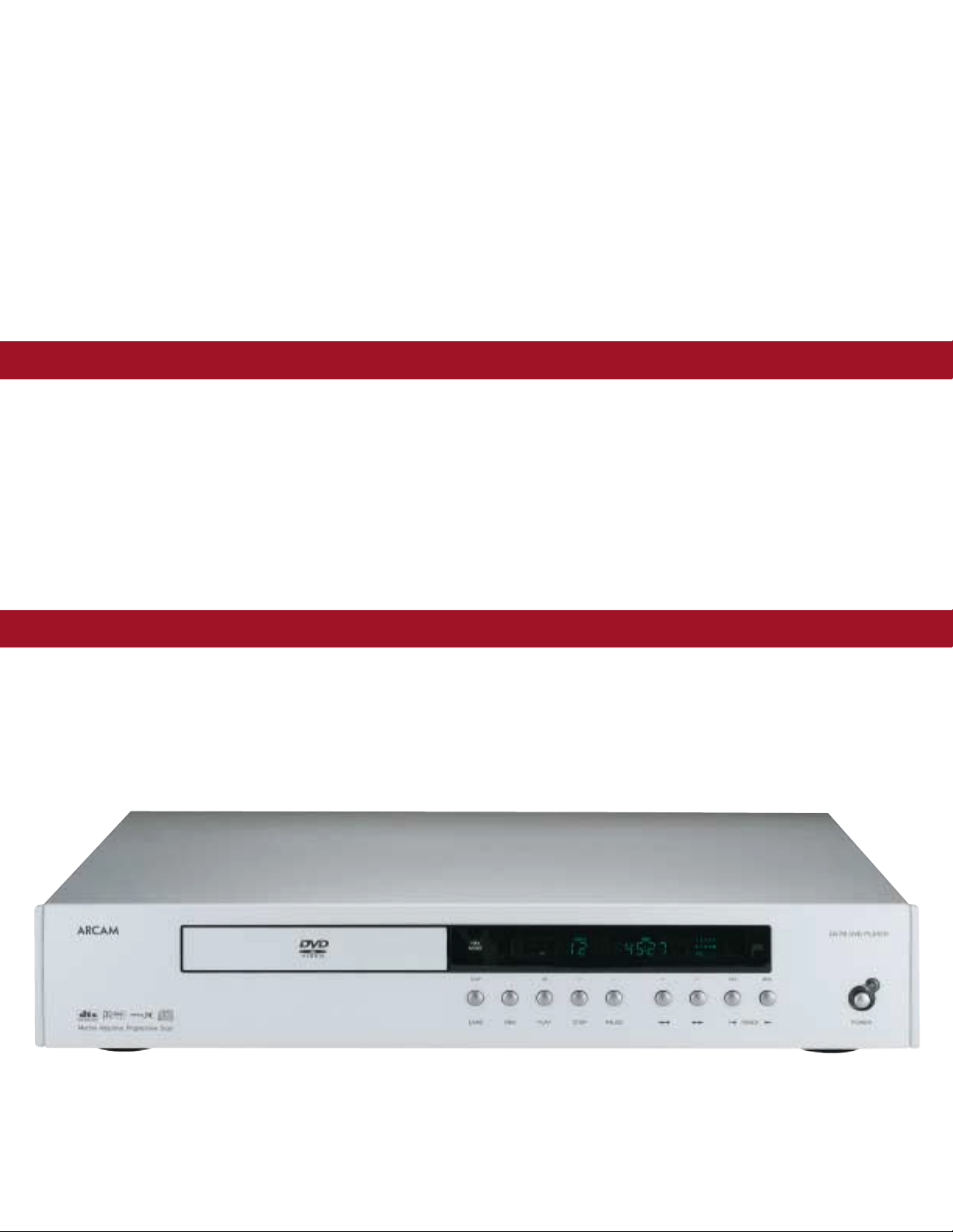
DV79 DVD Player
Service
Manual
Issue 1.0
ARCAM
Bringing music & movies to life
Page 2

DV79
Contents List
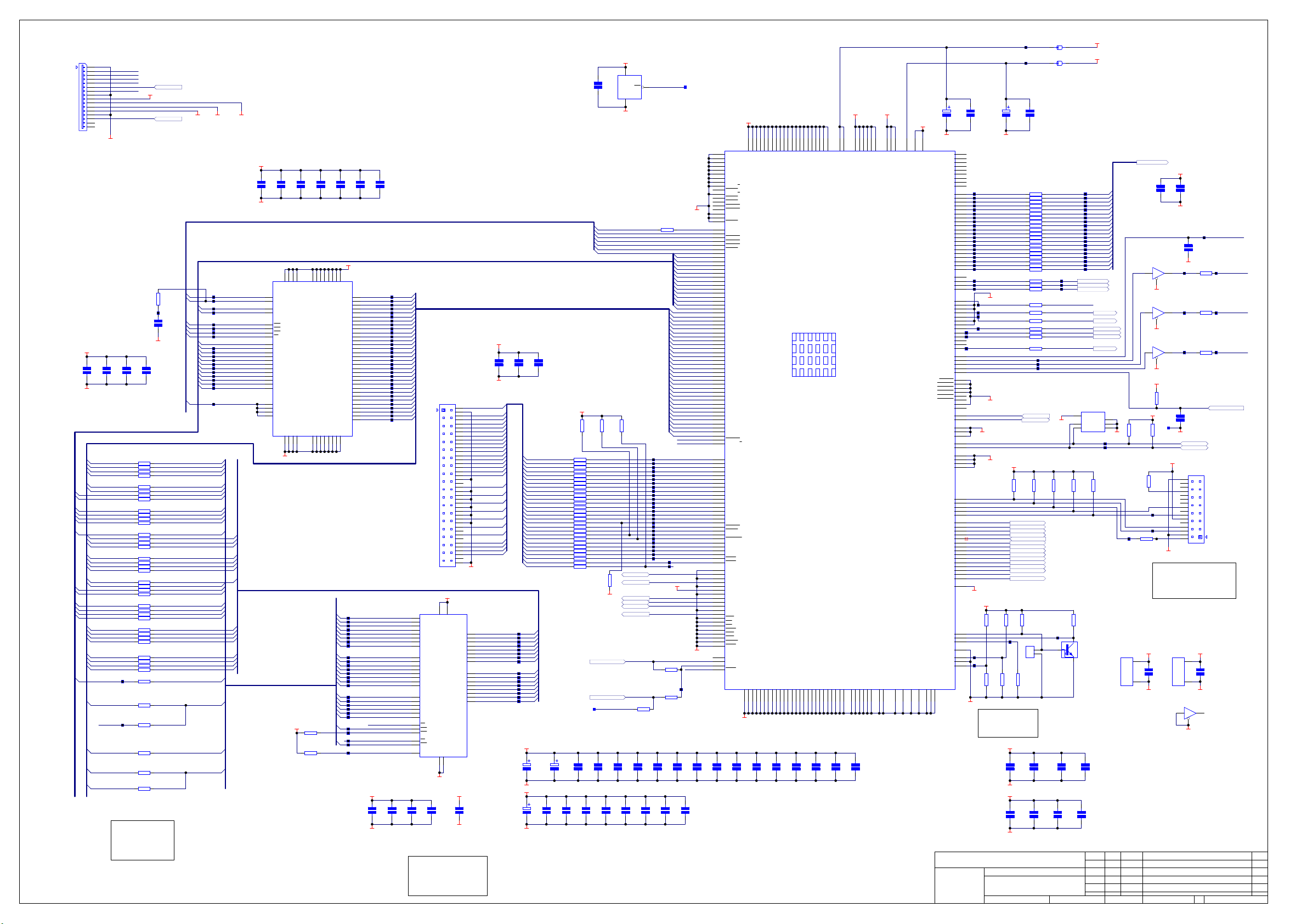
Circuit Description
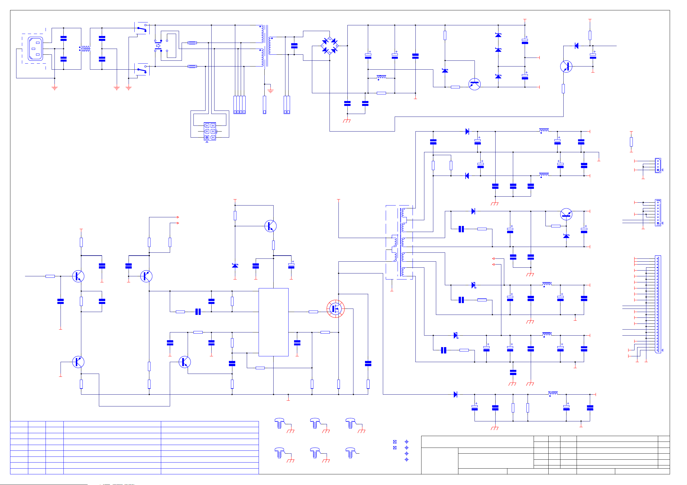
Power Supply L959AY
Display Board L961AY
Main Board L967AY (for serial numbers below D79V03175)
Main Board L974AY (for serial numbers above D79V03174)
Transformers
Mechanical Assembly
! CCT diagram
! Component layout diagram
! Parts list
! CCT diagram
! Component layout diagram
! Parts list
! CCT diagram
! Component layout diagram
! Parts list
! CCT diagram
! Component layout diagram
! Parts list
! L924TX
! L925TX
! Exploded view diagram
! Mechanical and packing part list
Page 3
Diva Dv79 Circuit description.
Overview
DiVa DV/79
The
and only shares it power supply board and display
board with the
The player is based around acclaimed
V
chipset coupled to high specification
converters for all six audio output channels and a
extremely high quality digital video encoder also
featured in this design is a HDMI output digital Video.
Power supply board.
Non-switching
Mains power arrives at
filtered by EMC choke LI and Y caps C3 and C4,
mains switch SW2a/b switches both Negative and Live
phases before the power reaches the mains select
switch at location SW1 the switch allows the primary
windings of the transformer TX1 to be wired in either
Parallel or Series configuration.
The Bridge rectifying Diode package at location D1
forms the basis of the conventional power stage and
supplies a VN35V6 (-35.6v) to the Switch mode
stage, transistor
DZ1
and allows for the series Zener diodes DZ2, DZ3,
DZ3 to supply the VN13V5 and VN19V rails.
We will also see a simple A.C present circuit this is
used for delayed output relay operation and fast relay
closure under interrupted supply conditions thus
preventing power down op-amp offsets from reaching
the Audio output sockets.
Switch mode
The switch mode supply is formed around the
Driver/Control chip
mode). The chip is referenced the –36.5V supply line
and the Digital ground DGND, the supply for the chip
is formed by the 12v Zener at location
seen on Pin 7 as VCC. The power supply allows for
the switch-mode to be tied the to Audio sampling
frequency for any given compatible format
is a completely new design platform
DV78
.
Zoran Vaddis
Wolfson
IEC
inlet socket
TR1
is biased by 2v7 Zener diode
IC1
UC3843 (used in regulating
SKT1
DZ6
D to A
and is
and can be
see Fig 1
.
Fig 1 PSU clock control
Fs
Frequency
select
44.1 kHz 0 0 44.1 kHz
48 kHz 0 0 48 kHz
88.2 kHz 0 1 44.1kHz
96 kHz 0 1 48 kHz
176.4 kHz 1 0 44.1 kHz
192 kHz 1 0 48 kHz
Others 1 1 OFF
PSUFS1
Pin 11
IC305a
PSUFS0
Pin 12
IC305a
PSUCLK
Output Pin 5
of IC305a
The PSU sync signal is driven into the power supply via
Resistor R9 if no Sync is present the unit is set to free run at
xxxx due to the RT/RC network attached to Pin 4.
IC1
is running in regulated mode and monitors the voltage
output on the +5V and +3V3 D.C lines, the two voltages are
summed by TR8 and Driven into the VFB and Comp inputs
of IC1, the Voltage is then regulated by changing the time
base of the PWM output at pin 6 (longer the time base the
lower the voltage), the PWM switching frequency is driven
into the switch-mode transformer by the high speed Nmos
device at position M1, R5 is used to sense the Current
across the gate of the Nmosfet and in the event of a short
circuit will safely shut the power supply down. We derive the
12v Mech supply from the output of M1 using the Ultra-fast
Diode at location D8 to rectify the
PWM line
.
The D.C outputs from the switch mode have extensive
switch mode noise removing filters these are seen as 100n
caps down to ground and Wire wound inductors in series
with the supply rail.
Power supply main board
All the power supply rails are supplied to the main board via
the 32 way FFC conector at location
CON1001
.
Digital
The
supplies from the switch mode stage of the
power supply arrive as 3V3D, +5VD and +12VD we also see
the Display board power supplies arrive as –19V, -9 and
–13.5V all of the supplies have a second stage of
implemented on the board to remove all traces of ultra-sonic
noise.
The 3V3D rail is the main 3V3 rail used to power the digital
circuitry; +5VD is used for all 5v Digital/Video supplies the
+12VD is used for Scart switching and to power the HDMI
circuit.
The 1V8 rail is derived from the 3V3 rail and is regulated by
the adjustable regulator at location
REG1003
.
Page 4

Analogue
The
as +15V3 and –15V3 rails these are filtered L1002 and
L1015 before being regulated by the adjustable
regulators at locations
provide +/- 12V rails for the Analogue output stage.
Regulator
forms the Audio DAC supply.
The Display board requires several supply voltages
these are simply passed through the main board,
being filtered on the way to prevent transmission of
noise through to the surrounding electronics. The
display takes the +5V, -19V, -13V5 and -9V the –13V5
and –9V form a floating 4.5V supply biased relative to
the –19V grid voltage.
Display Board
The main component of the Display board is
a Vacuum Florescent Display driver with keyboard san
and a serial data in/out interface.
The Chip receives display drive serial data from the
Vaddis V
13 and 14 these will be seen a DIN, STS and CLK this
data is used to drive the VFD a
with the VADDIS V and supplies Keyboard Scan
information. The keyboard scan is a 6 x 4 matrix with
the Key Source appearing at S3, S4, S5, S6 and the
Keyscan
Please see:
Infra red
The
data and send the data to the Vaddis V on the main
board via transistors TR2 and TR3, LED 2 is used to
mix the rear panel RC5, this is covered in-depth within
the Coms and Video output section of this guide.
supply stages arrive at the main board
REG1000
REG1001
chip on the main board via Con1 on pins 12,
data returns appearing a K2, K3 and K4.
above for
is fed from the +15V3 rail and
power supply
pick-up at location RXI receives RC5
REG1002
and
DOUT
line interfaces
information.
IC1
to
this is
Main Board electronics.
Zoran Vaddis V.
The main processor/control chip on the main board is the
Zoran Vaddis V at location
incarnation of the very popular Vaddis range of processors
and allows for a much lower component count when
compared to our earlier players as many of the playback
functions have moved onto the Vaddis V silicon.
Below you will see the
o 20 Bit digital video output for external Video
DAC’s and HDMI output stage.
Decoded Analogue Video output (internal
o
DAC) used on the DV78 only.
o Digital Audio output 3 data lines 6 channels for
internal L + R DAC’s and L + R + C + LS + RS
for DV79 and DV29 also used for HDMI for the
DV79 and DV29.
SPDIF output.
o
o Internal display interface.
Internal ATAPI interface.
o
o Internal IR interface.
Serial in/out for RS232
o
A more detailed explanation of the Vaddis V and
peripheral components follows.
Vaddis Power
The Vaddis V is powered by two separate supplies the
Vaddis requires a 1.8v supply for the core, this is regulated
from the 3.3v rail by
supply power to the I/P – O/P ports of the chip.
ATAPI interface
CON203
connector. This is decoupled from the Drive via an array of
decoupling resistors as required by the ATAPI spec.
is an ATAPI interface on a 40 way IDE
IC202
major functions
REG1003
, the 3.3v rail is used to
, this is the latest
of the Vaddis V
Page 5

Display Board interface
The display board interface is on the 16 way FFC flexi
foil connector at location CON202. Power for the
display also travels on the connector. There are 4 –
wires to interface with the VFD driver chip these are
seen as.
XFPDIN - Data to the display board
o
o FPDOUT - Data from the display board
o XFPCLK - Clock
o XFPSEL - Chip select
The above control lines are level shifted to 5v logic
from 3.3v levels by
IC200
(74HCT125) these are the
levels required by the VFD drive chip.
The IR output from the Display board arrives as
IRRCV
this is an open collector signal, which can be
wire-Ord with the re-panel remote input.
Digital Audio
The Digital audio leaves the chip 3 sets of data lines
labelled as.
o ADAT0 - Left and Right channel data
o ADAT1 - Left and Right surround
ADAT2 - Centre and Sub
o
Along with the ADAT line we will also see the
ALRCK
and
as required for IS2 data conversion.
ABCLK
The Vaddis V also supplies a direct SPDIF output for
interfacing with ancillary processing equipment.
Digital Video
The Digital Video output from the Vaddis V consists of
the following signals:
o VIDPO to 19 - 20 Bit wide digital video data
o CLK_27M - 27 Mhz Video clock
o VSYNC - Vertical sync
HSYNC - Horizontal Sync
o
The 20 bit wide bus
VIDP0
to 19 provides video data
as follows.
Interlaced video mode: VIDP0 to 7 provide
multiplexed 8 bit Y, Cb and Cr data with VIDPO being
the Isb.
Progressive scan video mode: VIDP0 to 9 provide
10 bit multiplexed Cb, Cr data with VIDP0 being the
VIDP10 to 19
Isb.
being the Isb.
provide 10 bit Y data with VIDP10
Flash/ SDRAM
IC203
is a 64Mbit (32 bit x 2Meg) SDRAM. It runs at
135MHz
IC205
is a 16Mbit (16 bit x 1Meg) intel type flash IC for
program storage (Player software).
The flash interfaces to the Vaddis V using the SDRAM bus
it may appear that the bus connects to the flash in a
random manner, however this is simply because the
Vaddis bus is multiplexed that way. The Flash will be
accessed at power up and the contents are copied to the
SDRAM the program will then be run from the SDRAM.
Series resistors are employed to isolate the flash bus from
the main SDRAM bus.
EEPROM
IC204 is a 8kBit (1K x 8) Serial EEPROM. This is used for
storage of non-volatile storage of player settings, region
settings and bookmark data.
Clocks
CLK27MV
is the 27Mhz clock for video. It is used to
generate the 135Mhz clock for the Vaddis microprocessor
and DSP. The MCLKV is the audio master clock for the
Vaddis.
We run the Vaddis in
PLL bypass
mode and generate or
own master clock (see main clock section of manual) for
higher accuracy and improved performance across Audio
and Video.
RESET
IC201
is a reset generator chip that monitors the +3.3V rail
and ensures a reset signal PWR_ON_RESET* is
generated on power up, or if the mains power dips below
an operational level.
This signal is used to reset the Vaddis V and Flash micro
only. The Vaddis V line labelled as RESET* resets the
remaining circuitry of the player apart from the HDMI chip,
this has it’s own reset line labelled as HDMI_RESET this is
necessary if we require to reset the HDMI chip only (for
example when the HDMI sink is connected and then
disconnected).
Serial Port
The VADDIS V can interface with the external world via
the RS232 connector at location CON900 and the RS232
Transceiver at location IC900, the serial data lines are
shown as SERIAL RX and SERIAL TX these lines allow
for direct control over the unit via RS232.
Page 6
O/P
Fig 2. GPIO control signals from the Vaddis V
Single Name I/P-
PSUFSO-1 Output
ENABLE_AV Output
16/9 Output
9190INT* Input
GAIN_SCALING Output
ML_8740_0-2 Output
MC Output
MD Output
FSELE0-1 Output
MUTE* Output
DDC_SDA,DDC,SCL I/O
PROG_INT* Output
HDMI_RESET* Output
RESET* Output
Function
Control PSU Clock
divider
SCART control High
in normal operation
and low in standby
Scart 16/9
anamorphic control
line
Interrupt signal
from SII9190 HDMI
transmitter
High for HDCD gain
scaling
SPI load signal for
Audio DACs 0,1 and
2 (see note 1)
SPI clock signal for
DAC control
SPI data signal for
DAC control
Frequency select
generator
Active low audio
mute signal
12C bus for DDC
channel on HDMI
interface
High for Progscan
mode, Low for
interlaced mode.
Controls Sil9130
data mux
Reset signal for
HDMI transmitter
System reset
Clocks and SPDIF stage.
IC300 is a SM8707E clock generator IC. This IC is
sensitive to noise on it’s power supply, which causes
clock jitter for this reason we have a independent Low
dropout – low noise
+3v3
power supply for the chip
based around the regulator at location REG300.
X300
is a
27Mhz
crystal that
IC300
uses to generate
all the video and audio clocks required by the system
the crystal sits on the XTI and XTO pins of the chip,
the 27Mhz output at Pin 4 (MO2) is used to drive the
Vaddis chip directly bypassing the internal PLL.
The frequency of the audio master is dependent on
the on the current audio sample rate (I.e the sample
rate required by the format CD=44.1Khz and
DVD=48khz etc) and this is set by the system micro
via the FSLO and FSEL1 this selects either the
22.5792Mhz
IC300 this may then be divided by 2 by the clock
divide chip at location IC306 depending on the status
24.576Mhz
or
clock from frequency from
of FSEL1. Therefore 4 clock frequencies may be
obtained to support all required audio samples rates.
Nand gate
IC303 is used to gate
FSEL1
with
ENABLE_AV (which is low in standby mode) as such
when in standby mode the audio clock is disabled.
Clock Buffer
IC301
us used to buffer the audio master clock. The circuit
is arranged so that each device that requires the audio
master clock has it’s own driver these are seen as.
o MCLK_DAC0 - Pin 18
o MCLK_DAC1 – Pin 16
MCLK_DAC2 – Pin 14
o
o MCLK_VADDIS – Pin 3
o MCLK_HDMI – Pin 9
We also run the
Mute Line
from the Vaddis V
IC301
this
can be seen on Pin 12 and drives transistor TR401, the
transistor pulls the relays
RLY400, RLY500, RLY600
to
ground and un-mutes the audio outputs.
IS2 Audio Data
IC302
and
IC309
are buffers for the 12S signals these
ensure that the signals travelling to the DAC’s are point to
point. IC302 deals with the ALRCK and ABCLK and
C309
I
ADAT0,1,2
the
all signal are split into three
separate lines for the three stereo DACS.
PSU Clock Divider
IC304
the PSU clock is always either 44.1kHz or 48Khz (
and
IC305
form a clock divide by 1, 2 or 4 to ensure
See fig
1 within the power supply description section).
This circuit will also switch the
PSUCLK
off when
switching between sample rates (the PSU will free run
when the PSUCLK is not present).
SPDIF Output
The SPDIF output consists of
IC308
implemented as a
inline buffer and parallel output buffer. Gate A buffers the
signal so that the SPDIF line from the VADDIS sees fewer
loads and form a feed to the Optical output transmitter,
gates B,C and D drive the SPDIF in parallel so that we can
drive a 75ohm load adequately. The resistors at the output
of IC308 are arrange so that the output will be
pk
when the output is terminated with a 75 ohm load at the
500mV pk-
same time the output impedance of the circuit is 75ohms
as required by the Sony Philips Digital Interface
specification, C315 provides AC coupling and L301
provides common mode noise rejection for EMC
performance.
Page 7

Left and Right channel D to A stages
Wolfson WM8740
The
and a +3V3 supply along with the Digital Audio data
lines already described in this guide.
Left channel output only
The
section as all audio output stages are the identical (all
six channels of a DV79) apart from the HDCD gain
switching for L + R only.
IC400B
Bessel filter with a differential input and a gain of 1 this
follow by a output buffer IC401B, the gain of IC401B is
control by the switching chip at location
normal use the Gain of IC401B is set to 1.1 but in
HDCD
in parele with R413 and the gain is set to 2.2 allowing
for the higher audio output required by the HDCD
standard.
C436 is a A.C coupling capacitor used to remove the
few mV of offset that the DAC produces, D400
provides protection against from ESD.
The all output relays are under control of the Vaddis
V chip but will also mute the outputs instantly under
mains failure conditions. Switching drive is provided
by TR401 (MUTE_BUF) and TR400 (AC_PRES) the
relays are in mute mode if either the input to TR401 is
Low or if the input to TR400 is high.
Please note:
outputs of the left/right audio stages.
Video Encoder
The video encoder at location IC703 is an Analogue
devices
interlaced and progressive scan video. It runs on a
2.5V supply provided by REG700 the voltage
reference for the chip of 1.225V is provided by
REF700 and should be seen on Pin 46. C730-731 and
R736 form an external PLL filter.
The Data lines into the encoder arrive as VIDP0 – 19
from the outputs of the VADDIS V chip.
The external current setting resistors for the internal
DACS are seen as R721-R722 and R738-R739 these
set the correct output level for the DACS.
The encoder gives out
S-Video (Y and C) and shared YUV/RGB signals. The
setting of the RGB or YUV mode is select with the
Video settings page of the Setup menu.
and associated components for a 2nd order
mode the
The
ADV7310
stereo DAC requires +5V(A)
will be described in this
IC402
IC402
switches a second 10k resistor
Scart
left/right audio is fed from the
video encoder, supporting
6 video signals
, for composite,
, in
six analogue output
The
o DAC_A = Composite
o DAC_B = SVID Y
DAC_C = SVID C
o
o DAC_D = Y or Green
o DAC_E = U or Blue
o DAC_F = V or Red
Please note: When the player is in Progressive scan
mode the composite and S-Video signals will be
switched off.
The Video outputs from IC703 are filtered by six identical
filters. For instance if we look at the Composite stage we
will see a very slow roll off filter comprising of C719,
C721 with L701 and L703 the
stage is around 40Mhz, resistors R700 and R702 form a
load for the current output DAC and as such set the
relative output level.
The outputs are driven by the Video op-amp at location
IC700A
75ohm resistor,
These signals now travel to the COMMS and Video
extension card on Con 901.
page 7.
SCART Output
RGB and Composite video signals as well as Left and
Right audio signals are all present on the SCART output
socket. As the RGB and YUV signals share the same
output port at the Vaddis V the player must be set to
RGB SCART
SCART.
RGB does not contain a Sync signal and the sync must
be taken from the Composite out (4 wire RGB).
Also present at the Scart are a number of control flags
for the monitor these include 2 GPIO control lines direct
from the Vaddis.
o
o 16/9
These are seen at the SCART output pins as.
o O/6/12
o RGB STAT
The 0/6/12 line (SCART pin 8) is used to inform the
monitor of the screen format being sent by the player as
set in the video set-up section of the software.
o
o 16:9 aspect ratio = 6V
o 4:3 aspect ration = 12V
The RGB status line (SCART pin 16) will be seen as 0v
= no RGB and >1v is RGB present.
this has a gain of
D701
operation to have a RGB output on the
Please note
ENABLE_AV
Standby = 0V
signals are seen as.
–3dB
point of the filter
2.15
and is terminated by a
forms protection against ESD.
See description
: When in RGB SCART mode the
on
Page 8

HDMI output stage
Please note:
Due to the plug and play nature of the
HDMI/DVI interface, if presented with a reported no
HDMI problem it is worth checking all set-up
parameters of both the DVD player and the
Plasma/Projector in use before performing component
level diagnostics on this product.
HDMI is a system that transmits uncompressed digital
video and digital audio over a high speed encrypted
interface.
IC1102 is an SII9190 HDMI transmitter IC in essence
the chip takes the Digital Video and Audio information
and sends the Data out in HDMI format.
REG1100 is used to generate a clean regulated 3V3
power supply to Pins 18 and 33 of the HDMI chip.
IC1100 –IC1101 are 3 state octal/line drivers these
form a multiplex that switches between the 2 groups of
signals for the video data input stage of the SII9190
the multiplexer is control by the Signal from the Vaddis
V labelled as PROG/INT this will sit at logic 1 for
Progressive scan and logic 0 for interlaced.
interlaced mode
In
VIDP7-0
are passed to input port pins
the 8 bit Y/Cb/Cr video data on
D15 – D8
of the
SII9190.
Progressive scan mode
In
all 20 bits of the Video
data bus are used and get mapped as follow.
VIDP 19 -12 provide 8 msbits of Y data to pins D15-8
VIDP 11 -10 provide 2Isbits of Y data to pins D2-3
VIDP 9 - 2 provide 8 msbits of Cb/Cr data to pins D23 – 16
VIDP 1 – 0 provide 2 Isbits of Cb/Cr data to pins D7 - 6
Along with the VIDP video data lines we must also see
VSYNC – Vertical sync data
HSYNC – Horizontal sync
CLK27M_VID – 27Mhz video clock.
SPDIF – Digital audio data
MCLK_HDMI – Used to strobe HDMI dig audio
output
At the
of the HDMI chip we will see the
following signals at SKT100.
TMDS
(Transistion Minimised Differential Signalling)
this consists of a clock signal (TXC+/TXC-) and
signals
(TX0+/TX0-, TX1+/TX1- and TX2+/TX2-)
3 data
.
All signals are differential and use current switching
techniques therefore
no signals
will be observed
unledd the output is correctly terminated. In this
application the clock signal will always be 27MHz and
the data signals will be clock X10 so 270Mbit/s.
DDC Channel
this is a 12C interface on DDC_SCL and
DDC_SDA. These signals connect to the VADDIS V
which is the I2C bus master, The DDC channel is used
to read back information from the HDMI sync regarding
it’s Video and Audio capabilities and is also used for
HDCP encryption authentication.
+5V Power, the HDMI interface requires a 5V supply
capable of delivering around 50mA, the supply is
provided by REG 1101 which delivers the required
current and will shut down in the event of a short circuit.
Hotplug.
The HDMI `Hot plug’ signal HDPIN is a +5V to
signal the presence of equipment being connected, this
converted to 3v3 logic 1 as IC1100 is not +5V tolerant.
CEC.
The CEC (Consumer Electronics Control) signal is
a 1-wire bidirectional control signal. It connects to the
Vaddis via an ESD protection circuit D1102 at the
moment this line is not used at present and is a optional
part of the HDMI specification.
Comms and Final video output stage
The signals from the main board travel up to the Comms
board on connector
CON902
.
The Video signals simply travel via an A-C coupling net
before exiting the player via the RCA-phono sockets at
locations
SKT902
and
SKT903
.
The RS232 interface is on 9 way “D” type CON900, with
IC900 providing the level translation and static protection
between the RS232 levels and the
required by the VADDIS V,
CON900
3.3V
CMOS levels
also supplies a
+5V
Status level when ever the unit is not in standby this
generated from a buffered version of the
AV_ENABLE
signal as used within the SCART output stage (0V in
standby).
We have two remote input bus’s on this board, the first
can be seen to arrive at
signal received should be a
SK901
on a 3.5mm mono jack
36Khz
modulated RC5
signal, the RC5 data then travels to the front panel and
is fed to IR led that is sited just behind the front panel
Sensor
, we use the sensor to demodulate the and opto-
IR
isolate the signal due to the fact that the signal is floating
up from ground.
The 3.5mm socket at location
un-modulated RC5 signals these take the form of a
5V/0V RC5 signal, with 5V representing a mark
SKT900
is used to receive
(equivalent to a burst of 36Khz carrier on infrared) and
the 0V representing a space (equivalent to no-infra-red
carrier), this input is effectively wire-Ord with the front
panel IR receiver on IRRCV.
Page 9
SW2A
DGND
SDDFC30400
SW1
18-000-0019
SW2B
SDDFC30400
C49
22N
100V
MKS2
5V_NFB
3V3_NFB
R7
6K8
0W25
MF
R4
4K7 0W25
MF
C15
100N
100V
MKS2
FHLDR1
20mm HLDR
FS1 T315mA
S504
FHLDR2
20mm HLDR
FS2
T315mA
S504
CON1
3
2
1
MOLEX
44472
(NFB From PSU Outputs)
C50
22N 100V
MKS2
R10
1K0 0W25
MF
TR4
BC546B
TO-92
VN35V6
2A22B
115V 230V
1A11B
MAINS SUPPLY
FOR EXT. AUDIO
SUPPLY TX
R11
9K1
0W25
MF
TR8
BC556B
TO-92
VN35V6
R26
68R
0W25
MF
R27
2K7
0W25
MF
USED TO SECURE TRANSFORMER CABLES TO PCB NEAR CON1
6
5
4
C51
22N
100V
MKS2
C16
100N
100V
MKS2
GREY
BLACK
3
4
GREY
DK GREY
CON2
WAGO
256
NOTE TRANSFORMER TX1 IS MOUNTED ON
THE CHASSIS AND CONNECTED TO THE PSU
PCB BY CON2,3,4. TX1 IS SHOWN ABOVE FOR
CIRCUIT OPERATION
DGND
R12
10K
0W25
MF
R14
NF
R15
10K
0W25
MF
C56
4N7
100V
CER
R28
22R
0W25
MF
SKT1
BULGIN
PX0580
SH1
NF
EMC Shield
N
E
L
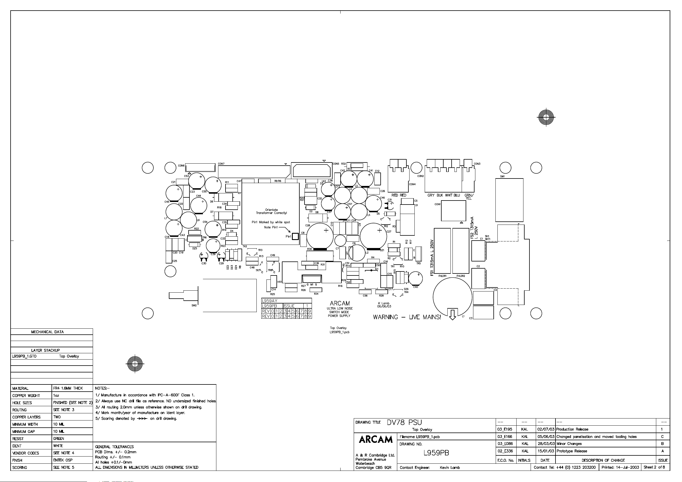
QTY DESCRIPTIONPART No. NOTESITEM
R9
1K0 0W25
MF
PSU_CLK
ITEM1 1 Clip For SW Profile HeatsinkF006
ITEM2 1 Sil Pad For TO-220 HS InsulatorF082
ITEM3 2 Fuseholder Cover For 20mm FuseholderF022
ITEM4 1 Blank PCB DV78 PSUL959PB
ITEM6 1 Cable Tie 100MM X 2.5MMF044
ITEM5 1 Earth Lead Assy 75MM8M101 SAFETY EARTH WIRE FROM IEC INLET SK1 TO METAL CHASSIS
ITEM7 2 Rivet CopperHP007S RIVETS TO SECURE IEC INLET TO PCB
C1 C3
NF
4
1
C2
NF
VP5V
C47
22P
100V
N150
DGND
DGND
R8
1K0
0W25
MF
TR3
BC546B
TO-92
R13
10K
0W25
MF
TR7
BC556B
TO-92
R25
100R
0W25
MF
3N3
250V
3
CER
L1
250U
2
C4
3N3
250V
CER
C14
100N
100V
MKS2
VN35V6
C48
1N0
100V
CER
WHITE
BLUE
2
1
BLUE
LT GREY
DZ6
BZX79C
12V
DO-35
1
115V
2
3
115V
4
C17
100N
100V
MKS2
VN35V6 VN35V6VN35V6
2
VFB
1
COMP
8
VREF
4
RT/CT
R29
82K 0W25
MF
TX1
Small Toroidal Mains
L924TX
7
1
GREEN
CON3
WAGO
256
7
VCC
GND
5
FIX1
Dia 3.5mm
FIX2
Dia 3.5mm
5
6
TR5
BD179
TO-126
R17
10R
0W25
MF
OUT
ISEN
1
GREY2GREY
CON4
WAGO
256
VN35V6
1
1
C40
220UF
16V
YXF
IC1
UC3843AN
DIP-8
6
3
VN35V6
C5
NF
33R 0W25
C52
330P
100V
N750
R24
MF
R16
47K
0W25
MF
FIX3
Dia 3.5mm
FIX4
Dia 3.5mm
HS1B
SW38-2
10.2C/W
R5
4K7 0W25
MF
1
1
D1
2KBP02
DGND
M1
IRF640N
TO-220
R30
0R22
3W
SPRX
FIX5
Dia 3.5mm
FIX6
Dia 3.5mm
C6
100N
100V
MKS2
1
1
C27
1000UF
63V
YK
L2
NF
LK1
0R0 0W 25 MF
C7
100N
100V
MKS2
TX2
Ferrite Switch Mode
L925TX
C36
1N0
100V
CER
R31
10R
0W25
MF
C28
1000UF
63V
YK
1 11
16T
2
16T
3
SCR
DGND
FD1
FD2
41T
41T
22T
14T
10T
VN35V6
4
5
6
12
9
10
7
8
TOOL1
TOOL2
TOOL3
TOOL4
C8
100N
100V
MKS2
C32
470pF
1kV
DE
R20
470R
0W25
MF
1N0 100V
DRAWING TITLE
A & R Cambridge Ltd.
Pembroke Avenue
Waterbeach
Cambridge CB5 9PB
R1
22K
0W25
MF
DZ1
BZX79C
2V7
DO-35
R2
220R
0W25
MF
D6
31DQ10 DO-201AD
C34
CER
D8
UF5406
DO-201AD
TR1
BC547B
TO-92
D2
UF4003
DO-41
R21
470R
0W25
D3
MF
UF4003
DO-41
D4
UF4003
DO-41
C33
1N0 100V
CER
NFB (To Controller E/A)
D7
31DQ06 DO-201AD
C35
1N0 100V
CER
R18
10R 0W25
MF
DV78 SERIES PSU
Filename:
Notes:
Contact Engineer:
C37
100UF
50V
YXF
C38
100UF
50V
YXF
R23
33R 0W25
MF
5V_NFB
3V3_NFB
R19
10R 0W25
MF
C57
470UF
25V
YXF
L959_1.1.sch
C53
1000UF
16V
YXF
C9
100N
100V
MKS2
C24
100N
100V
MKS2
DZ2
BZX79C
10V
DO-35
DZ3
BZX79C
3V3
DO-35
DZ4
BZX79C
5V6
DO-35
DGND
C29
22UF
63V
YK
VN13V5_F1
C30
22UF
63V
YK
VN19V
L3
33U 1.17A 8RHT2
L4
33U 1.17A 8RHT2
C10
100N
100V
MKS2
C39
220UF
16V
YXF
C18
100N
100V
MKS2
C54
1000UF
16V
YXF
C55
1000UF
16V
YXF
C25
100N
100V
MKS2
R32
NF
Contact Tel: (01223) 203200Kevin Lamb
C11
100N
100V
MKS2
470R 0W25
C19
100N
100V
MKS2
L6
6U8 2.1A 8RHT2
C20
100N
100V
MKS2
L7
6U8 2.1A 8RHT2
C21
100N
100V
MKS2
33U 1.17A 8RHT2
R33
1K0
0W25
MF
ECO No. DESCRIPTION OF CHANGE
L5
INITIALS
Printed:
R22
MF
R3
4K7
0W25
MF
C41
470UF
25V
YK
C42
470UF
25V
YK
C44
470UF
25V
YK
C45
470UF
25V
YK
DATE
22-Apr-2004
D5
1N4148
DO-35
TR2
BC546B
TO-92
TR6
BD179
TO-126
DZ5
BZX79C
5V1
DO-35
DGND
DGND
C46
470UF
25V
YK
DGND
Make CON1 fitted (used in DV29)22/04/04PG04_E046
Production release02/07/03KAL03_E195
VP5V
C12
100N
100V
MKS2
DGND
C13
100N
100V
MKS2
C43
470UF
25V
YK
C22
100N
100V
MKS2
C23
100N
100V
MKS2
1 1Sheet of
R6
6K8
0W25
MF
C31
22UF
63V
YK
VP15V5
AGND
VN15V5
VN9V_F2
VN13V5_F1
VP5V
VP3V3
VP12V
C26
100N
100V
MKS2
AC_PRES*
AGND
DGND
VP5V
VP12V
VP5V
VP3V3
SPARE1
SPARE2
VN19V
VN9V_F2
VN13V5_F1
VP3V3
VP3V3
VP3V3
VP3V3
VP3V3
VP3V3
SPARE3
SPARE4
VP5V
VP5V
VP5V
PSU_CLK
AC_PRES*
VP12V
VP15V5
VN15V5
DRAWING NO.
LK2
NF
DGND
DGND
DGNDAGND
L959CT
CON5
4
3
2
1
Amp
HD Pwr Con
CON6
8
7
6
5
4
3
2
1
AMP
CT
NF
CON7
32
31
30
29
28
27
26
25
24
23
22
21
20
19
18
17
16
15
14
13
12
11
10
9
8
7
6
5
4
3
2
1
MOLEX
52045
1.1
1.0
ISSUE
Page 10
Page 11

DV79 DVD player PSU board L959AY issue 1.1.1
Designator Part Description
C1 2J410 Capacitor SM 0805 X7R Ceramic 10% 50V 100N
C2 2J410 Capacitor SM 0805 X7R Ceramic 10% 50V 100N
C3 2J410 Capacitor SM 0805 X7R Ceramic 10% 50V 100N
C4 2J410 Capacitor SM 0805 X7R Ceramic 10% 50V 100N
C5 2MA610 Capacitor Surface Mount Electrolytic 10UF 50V 6.3 X 4.5MM
C6 2MA610 Capacitor Surface Mount Electrolytic 10UF 50V 6.3 X 4.5MM
C7 2MA610 Capacitor Surface Mount Electrolytic 10UF 50V 6.3 X 4.5MM
C8 2L210 Capacitor SM 0805 NPO Ceramic 5% 100V 1N0
C9 2L210 Capacitor SM 0805 NPO Ceramic 5% 100V 1N0
C10 2L210 Capacitor SM 0805 NPO Ceramic 5% 100V 1N0
C11 2L210 Capacitor SM 0805 NPO Ceramic 5% 100V 1N0
CON1 8K8616 Con 1.0MM Horiz FFC 16WAY 52807 Series
D1 3AS16W Diode Surface Mount Small Signal BAS16W SOT-23 Package
D2 3AS16W Diode Surface Mount Small Signal BAS16W SOT-23 Package
D3 3AS16W Diode Surface Mount Small Signal BAS16W SOT-23 Package
D4 3AS16W Diode Surface Mount Small Signal BAS16W SOT-23 Package
DISP1 B1014 Display DV88
IC1 5H6312 IC VFD Driver PT6312LQ SM LQFP-44 package
LED1 3D007 LED 3.1mm Green SLR-37MG3T
LED2 3D010 LED SM Red SML-010LT
LED3 3D007 LED 3.1mm Green SLR-37MG3T
LED5 3D006 LED 3mm Red/Green Tri-Colour L-93WEGW
R1 1M133 Resistor 0805 Surface Mount 0.125W 1% 330R
R2 1M133 Resistor 0805 Surface Mount 0.125W 1% 330R
R3 1M133 Resistor 0805 Surface Mount 0.125W 1% 330R
R4 1M122 Resistor 0805 Surface Mount 0.125W 1% 220R
R5 1M118 Resistor 0805 Surface Mount 0.125W 1% 180R
R6 1M139 Resistor 0805 Surface Mount 0.125W 1% 390R
R8 1M310 Resistor 0805 Surface Mount 0.125W 1% 10K
R9 1M310 Resistor 0805 Surface Mount 0.125W 1% 10K
R10 1M247 Resistor 0805 Surface Mount 0.125W 1% 4K7
R11 1M356 Resistor 0805 Surface Mount 0.125W 1% 56K
R13 1M310 Resistor 0805 Surface Mount 0.125W 1% 10K
R14 1M310 Resistor 0805 Surface Mount 0.125W 1% 10K
R15 1M310 Resistor 0805 Surface Mount 0.125W 1% 10K
RX1 B2109 IR Receiver Module Kodenshi KSM-902TM1N
SW1 A1511 Switch Tact Low Profile No Gnd Pin
SW2 A1511 Switch Tact Low Profile No Gnd Pin
SW3 A1511 Switch Tact Low Profile No Gnd Pin
SW4 A1511 Switch Tact Low Profile No Gnd Pin
SW5 A1511 Switch Tact Low Profile No Gnd Pin
SW6 A1511 Switch Tact Low Profile No Gnd Pin
SW7 A1511 Switch Tact Low Profile No Gnd Pin
SW8 A1511 Switch Tact Low Profile No Gnd Pin
SW9 A1511 Switch Tact Low Profile No Gnd Pin
TR2 4D10KN Digital Transistor MMUN2211LT1 SOT23 Package
TR3 4A849B Transistor BC849B SOT23 Package
TR4 4A849B Transistor BC849B SOT23 Package
TR5 4D10KP Digital Transistor MMUN2111LT1 SOT23 Package
Page 12
IR REMOTE SENSOR
Pins 1-4 (SW1-4) are set
When creating BOM, import CSV into database then manually change quantity to 0.07 for ITEM4 (F238
+5VD
C1
100N
50V
0805
DGND
C8
1N0
100V
0805
DGND DGND DGNDDGND
FD1 FD2
TOOL1 TOOL2 TOOL3 TOOL4
+5V
GND
LED2
SM
RED
SML-010
LED2 is underneath infra red receiver.
The LED is lit by the remote bus signal,
allowing the infra red receiver to
demodulate the remote bus signal.
P18
RX1
O/P
KSM-902TM1N
P19
C10
1N0
100V
0805
R2
330R
0W125
0805
CHS
R8
10K
0W125
0805
TR2
MMUN2211LT1
SOT-23
C9
1N0
100V
0805
P16
C11
1N0
100V
0805
R9
10K
0W125
0805
TR3
BC849B
SOT-23
C6
10UF
50V
SM
SW6
1
2
SW7
1
2
SW8
1
2
SW9
1
2
K4
to read 0001, to be read
by display self test in
software
PLAY
STOP
LOAD
>>
D1
D2
BAS16
SOT-323
D3
BAS16
SOT-323
D4
BAS16
SOT-323
+5VD
BAS16
SOT-323
R10
4K7
0W125
0805
R1
330R
0W125
0805
DGND
-19V
+5VD
GR434GR335GR236GR1
C2
100N
50V
0805
GR5
GR6
VEE
SG11
SG10
SG9
P12
P13
P17
33
G5
G6
32
31
G7
30
S15
S14
29
S13
28
27
26
S12
25
S11
24
S10
23
S9
DVDA_LED*
S3
S4
ON/STBY*_LED
S5
S6
NAV_LED*
+5VD
DGND
+5VD DGND
K2
+5VD
DGND
K[2..4]
DGND
R11
56K
0W125
0805
P20
1
SW1
2
SW2
3
SW3
4
SW4
5
DOUT
6
DIN
7
GND
8
CLK
9
STB
10
K1
11
K2
44
K312K413VDD14SG1/KS115SG2/KS216SG3/KS317SG4/KS418SG5/KS519SG6/KS620SG721SG8
K4
K3
DGND
42
GND43OSC
IC1
PT6312LQ
LQFP-44
S1S2S3S4S5S6S7
+5VD
C4
100N
50V
0805
G1G2G3
G4
37
38
VDD
LED439LED340LED241LED1
SG16/GR7
SG15/GR8
SG14/GR9
SG13/GR10
SG12/GR11
22
S8
LED1
TR4
BC849B
SOT-23
R4
220R
0W125
0805
NF
R3
330R
0W125
0805
F11F12G15G26G37G48G59G610G7
Note that G1..7 are deliberately
reversed here, to be the same as
previous design (software takes it into
account)
C3
100N
50V
0805
P14
+5VD
3mm
GRN
LED 3mm
+5VD
R5
180R
0W125
0805
DGND
LED3
DISP1
SAMSUNG
SVV-07MS09
11
G1G2G3G4G5G6G7
DVD-A
TR5
MMUN2111LT1
SOT-23
P15
R6
390R
0W125
0805
REDGRN
+5VD
3mm
GRN
LED 3mm
LED5
3mm
BICOL
LED 3mm
VFD
POWER
NAV
S125S226S327S428S529S630S731S832S933S1034S1135S1236S1337S1438S1539F242F2
S1S2S3S4S5S6S7S8S9
S10
43
-9V_F2-13V5_F1
S11
S12
S13
S14
S15
R13
10K
0W125
0805
R14
10K
0W125
0805
R15
10K
DOUT
CLK
STB
DIN
REM_P
IRRCV
REM_N
0W125
0805
DGND
NF
CON1
16
MOLEX
52807
15
14
13
12
11
10
9
8
7
6
5
4
3
2
1
DGND
P2
P3
P4
P5
P6
P7
P8
P9
P10
P11
P1
SW1
MODE
1
2
SW2
<<
1
2
K2
K3
+5VD
DGND
C5
10UF
50V
SM
SW3
1
SW4
1
SW5
1
>|
2
|<
2
PAUSE
2
C7
10UF
50V
SM
DGND
-19V
-9V_F2
-13V5_F1
NOTE TO ENGINEERS:
tape)
This is the only way to ensure it appears as 0.07m on the BOM report
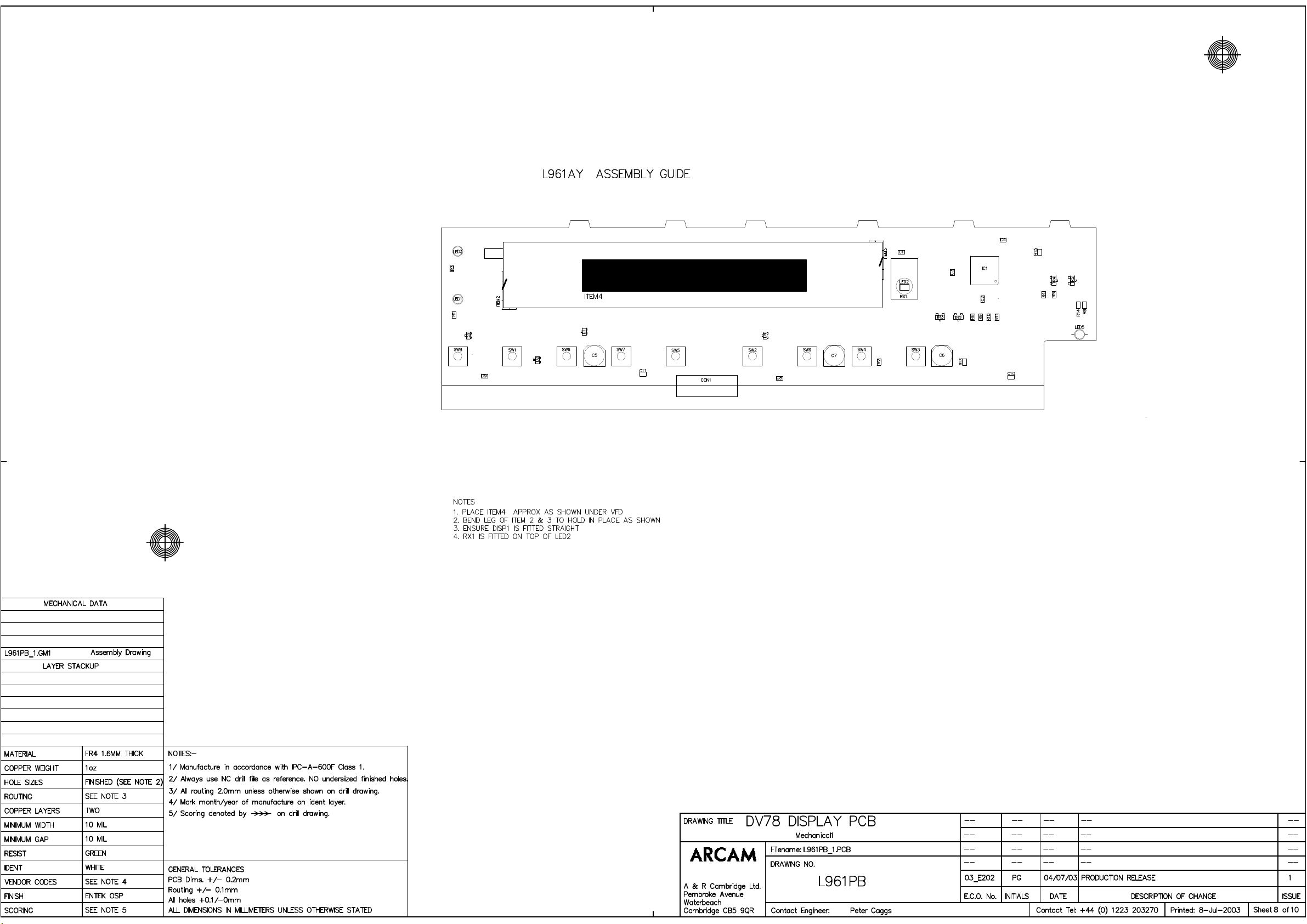
ITEM1 BLANK PCB DV78 DISPLAY BOARD1 L961PB
ITEM2 1
ITEM3 1
ITEM4 1 Foam D/S ADH BK 3MM Thk 10MM Wide RA106 10M ReelF238
F231
F231
VFD CORNER LOCATOR
VFD CORNER LOCATOR
70mm of 10mm wide double sided tape under VFD
DRAWING TITLE
A & R Cambridge Ltd.
Pembroke Avenue
Waterbeach
Cambridge CB5 9QR
DV78/DV79 DISPLAY BOARD
Filename:
L961_1.3.Sch
Notes:
Contact Engineer:
Contact Tel: (01223) 203270Peter Gaggs
PG 17-09-04 CHANGE RX1 TO KSM-902TM1N FOR BETTER PERFORMANCE 1.304_E140
PG 12-01-04 ADD DVD-A LED FOR DV79 1.204_E007
PG 02-09-03 CHANGE FOAM TAPE FROM F163 TO F238 (DOUBLE SIDED) 1.103_E260
PG 04-07-03 INITIAL SCH 1.003_E202
INITIALS
Printed:
DATE
17-Sep-2004
1 1Sheet of
ECO No. DESCRIPTION OF CHANGE
A2
DRAWING NO.
ISSUE
L961
Page 13
Page 14

DV79 DVD player Display board L961AY issue 1.3.0
Designator Part Description
C1 2J410 Capacitor SM 0805 X7R Ceramic 10% 50V 100N
C2 2J410 Capacitor SM 0805 X7R Ceramic 10% 50V 100N
C3 2J410 Capacitor SM 0805 X7R Ceramic 10% 50V 100N
C4 2J410 Capacitor SM 0805 X7R Ceramic 10% 50V 100N
C5 2MA610 Capacitor Surface Mount Electrolytic 10UF 50V 6.3 X 4.5MM
C6 2MA610 Capacitor Surface Mount Electrolytic 10UF 50V 6.3 X 4.5MM
C7 2MA610 Capacitor Surface Mount Electrolytic 10UF 50V 6.3 X 4.5MM
C8 2L210 Capacitor SM 0805 NPO Ceramic 5% 100V 1N0
C9 2L210 Capacitor SM 0805 NPO Ceramic 5% 100V 1N0
C10 2L210 Capacitor SM 0805 NPO Ceramic 5% 100V 1N0
C11 2L210 Capacitor SM 0805 NPO Ceramic 5% 100V 1N0
CON1 8K8616 Con 1.0MM Horiz FFC 16WAY 52807 Series
D1 3AS16W Diode Surface Mount Small Signal BAS16W SOT-23 Package
D2 3AS16W Diode Surface Mount Small Signal BAS16W SOT-23 Package
D3 3AS16W Diode Surface Mount Small Signal BAS16W SOT-23 Package
D4 3AS16W Diode Surface Mount Small Signal BAS16W SOT-23 Package
DISP1 B1014 Display DV88
IC1 5H6312 IC VFD Driver PT6312LQ SM LQFP-44 package
LED1 3D007 LED 3.1mm Green SLR-37MG3T
LED2 3D010 LED SM Red SML-010LT
LED3 3D007 LED 3.1mm Green SLR-37MG3T
LED5 3D006 LED 3mm Red/Green Tri-Colour L-93WEGW
R1 1M133 Resistor 0805 Surface Mount 0.125W 1% 330R
R2 1M133 Resistor 0805 Surface Mount 0.125W 1% 330R
R3 1M133 Resistor 0805 Surface Mount 0.125W 1% 330R
R4 1M122 Resistor 0805 Surface Mount 0.125W 1% 220R
R5 1M118 Resistor 0805 Surface Mount 0.125W 1% 180R
R6 1M139 Resistor 0805 Surface Mount 0.125W 1% 390R
R8 1M310 Resistor 0805 Surface Mount 0.125W 1% 10K
R9 1M310 Resistor 0805 Surface Mount 0.125W 1% 10K
R10 1M247 Resistor 0805 Surface Mount 0.125W 1% 4K7
R11 1M356 Resistor 0805 Surface Mount 0.125W 1% 56K
R13 1M310 Resistor 0805 Surface Mount 0.125W 1% 10K
R14 1M310 Resistor 0805 Surface Mount 0.125W 1% 10K
R15 1M310 Resistor 0805 Surface Mount 0.125W 1% 10K
RX1 B2109 IR Receiver Module Kodenshi KSM-902TM1N
SW1 A1511 Switch Tact Low Profile No Gnd Pin
SW2 A1511 Switch Tact Low Profile No Gnd Pin
SW3 A1511 Switch Tact Low Profile No Gnd Pin
SW4 A1511 Switch Tact Low Profile No Gnd Pin
SW5 A1511 Switch Tact Low Profile No Gnd Pin
SW6 A1511 Switch Tact Low Profile No Gnd Pin
SW7 A1511 Switch Tact Low Profile No Gnd Pin
SW8 A1511 Switch Tact Low Profile No Gnd Pin
SW9 A1511 Switch Tact Low Profile No Gnd Pin
TR2 4D10KN Digital Transistor MMUN2211LT1 SOT23 Package
TR3 4A849B Transistor BC849B SOT23 Package
TR4 4A849B Transistor BC849B SOT23 Package
TR5 4D10KP Digital Transistor MMUN2111LT1 SOT23 Package
Page 15
L967C2
L967C2.sch
VADDIS V
SHEET 2
GAIN_SCALING
RESET*
ML_8740_0
ML_8740_1
ML_8740_2
FSEL0
FSEL1
PSUFS0
PSUFS1
ADAT0
ADAT1
ADAT2
ABCLK
ALRCLK
SPDIF
MUTE*
CLK27M_VADDIS
MCLK_VADDIS
MD
MC
GAIN_SCALING
RESET*
MD
MC
ML_8740_0
ML_8740_1
ML_8740_2
FSEL0
FSEL1
PSUFS0
PSUFS1
ADAT0
ADAT1
ADAT2
ABCLK
ALRCLK
SPDIF
MUTE*
CLK27M_VADDIS
MCLK_VADDIS
ENABLE_AV
L967C3
L967C3.Sch
FSEL0
FSEL1
PSUFS0
PSUFS1
ADAT0
ADAT1
ADAT2
ABCLK
ALRCLK
SPDIF
MUTE*
CLK27M_VADDIS
MCLK_VADDIS
ENABLE_AV
CLOCKS
SHEET 3
PSUCLK
ADAT_DAC0
ABCLK_DAC0
ALRCLK_DAC0
MCLK_DAC0
MUTE_BUF*
ADAT_DAC1
ABCLK_DAC1
ALRCLK_DAC1
MCLK_DAC1
ADAT_DAC2
ABCLK_DAC2
ALRCLK_DAC2
MCLK_DAC2
PSUCLK
ADAT_DAC0
ABCLK_DAC0
ALRCLK_DAC0
MCLK_DAC0
MUTE_BUF*
ADAT_DAC1
ABCLK_DAC1
ALRCLK_DAC1
MCLK_DAC1
ADAT_DAC2
ABCLK_DAC2
ALRCLK_DAC2
MCLK_DAC2
AC_PRES*
MD
MC
RESET*
MD
MC
RESET*
L967C10
L967C10.Sch
PSUCLK
POWER
AC_PRES*
SHEET 10
L967C4
L967C4.Sch
AC_PRES* SCART_LEFT
GAIN_SCALING
RESET*
MD
MC
ML_8740_0
SCART_RIGHT
DAC L&R
SHEET 4
ADAT_DAC0
ABCLK_DAC0
ALRCLK_DAC0
MCLK_DAC0
MUTE_BUF*
L967C5
L967C5.Sch
MD
MC
ML_8740_1
RESET*
ADAT_DAC1
ABCLK_DAC1
ALRCLK_DAC1
MCLK_DAC1
CENTRE_OUT
SUB_OUT
L967C6
L967C6.Sch
MD
MC
ML_8740_2
RESET*
ADAT_DAC2
ABCLK_DAC2
ALRCLK_DAC2
MCLK_DAC2
DAC LS&RS
SHEET 5
DAC C & SUB
SHEET 6
CENTRE_OUT
SUB_OUT
SCART_LEFT
SCART_RIGHT
CEC
9190INT*
PROG/INT*
DDC_SDA
DDC_SCL
SDA
SCL
HDMI_RESET*
VIDP[0..19]
HSYNC*
VSYNC*
CLK_27M_VID
16/9
ENABLE_AV
IRRCV
SERIAL_TX
SERIAL_RX
REM_BUS_P
REM_BUS_N
CEC
9190INT*
PROG/INT*
DDC_SDA
DDC_SCL
SDA
SCL
HDMI_RESET*
VIDP[0..19]
HSYNC*
VSYNC*
CLK_27M_VID
16/9
ENABLE_AV
IRRCV
SERIAL_TX
SERIAL_RX
REM_BUS_P
REM_BUS_N
ABCLK_HDMI
MCLK_HDMI
ABCLK_HDMI
MCLK_HDMI
ADAT0
ADAT1
ADAT2
ALRCLK
RESET*
L967C11
L967C11.Sch
ADAT0
ADAT1
ADAT2
ABCLK_HDMI
ALRCLK
MCLK_HDMI
HDMI
SPDIF
CEC
9190_INT*
PROG/INT*
DDC_SDA
DDC_SCL
SDA
SCL
HDMI_RESET*
VIDP[0..19]
HSYNC*
VSYNC*
CLK27M_VID
L967C7
L967C7.Sch
SDA
SCL
RESET*
VIDP[0..19]
HSYNC*
VSYNC*
CLK27M_VID
SHEET 11
SCART_COMPOSITE
SCART_RED
SCART_GREEN
SCART_BLUE
VIDEO ENCODER
SHEET 7
COMPOSITE
SVID_Y
SVID_C
SCART_COMPOSITE
SCART_RED
SCART_GREEN
SCART_BLUE
COMPOSITE
Y
Y
U
U
V
V
SVID_Y
SVID_C
L967C8
L967C8.Sch
SCART_LEFT
SCART_RIGHT
16/9
ENABLE_AV
SCART
SHEET 8
SCART_COMPOSITE
SCART_RED
SCART_GREEN
SCART_BLUE
L967C9
L967C9.Sch
COMPOSITE
Y
U
V
SVID_Y
SVID_C
COMMS, VIDEO OUT
ENABLE_AV
IRRCV
SERIAL_TX
SERIAL_RX
REM_BUS_P
REM_BUS_N
SHEET 9
ITEM100 1 Blank PCB DV79 Main BoardL967PB
DRAWING TITLE
A & R Cambridge Ltd.
Pembroke Avenue
Waterbeach
Cambridge CB5 9QR
DV79 MAIN BOARD TOP LEVEL
Filename:
Notes:
Contact Engineer:
L967C1.Prj
PG 1.0
03_E020 19-02-04 Production release
Contact Tel: (01223) 203270Peter Gaggs
ECO No. DESCRIPTION OF CHANGE
INITIALS
Printed:
DATE
19-Feb-2004
1 11Sheet of
A2
DRAWING NO.
ISSUE
L967C1
Page 16
FRONT PANEL
CON202
1
2
FPDOUT
XFPCLK
3
XFPSEL
4
XFPDIN
5
REM_BUS_P
6
IRRCV
7
8
9
10
11
12
13
14
REM_BUS_N
15
16
MOLEX
DGND
52806
SDRAM DECOUPLING
+3V3D
C212
C213
100N
100N
16V
16V
0603
0603
DGND
address
data
RAMDAT5
RP200A
RAMDAT6
RP200B
RAMDAT11 FRAMDAT11
RP200C
RAMDAT10 FRAMDAT10
RP200D
RAMDAT9
RP201A
RAMDAT8
RP201B
RAMADD9
RP201C
RAMADD8
RP201D
RAMADD7
RP202A
RAMADD6
RP202B
RAMADD5
RP202C
RAMADD4 FRAMADD4
RP202D
RAMADD3 FRAMADD3
RP203A
RAMDAT31
RP203B
RAMDAT30
RP203C
RAMDAT29
RP203D
RAMDAT28
RP204A
RAMDAT27
RP204B
RAMDAT26
RP204C
RAMDAT25
RP204D
RAMDAT24
RP205A
RAMDAT7
RP205B
RAMBA0
RP205C
RAMBA1
RP205D
RAMADD10
RP206A
RAMADD0
RP206B
RAMADD1
RP206C
RAMADD2 FRAMADD2
RP206D
RAMDAT16
RP207A
RAMDAT17
RP207B
RAMDAT18
RP207C
RAMDAT19
RP207D
RAMDAT20
RP208A
RAMDAT21
RP208B
RAMDAT22
RP208C
RAMDAT23
RP208D
RAMADD11
PR252
PNVMR/B* NF(AMD)
PF243
RAMDAT3
RAMDAT4 NF(AMD 16Mb)
RAMDAT12
Use these resistors to configure for
Intel/AMD 8Mbit, 16Mbit, 32Mbit or
64Mbit devices
Intel 32Mbit is used for DV79
+5V_DISPLAY
PR253
C214
100N
16V
0603
1 8
2 7
1 8
2 7
1 8
2 7
1 8
2 7
1 8
2 7
1 8
2 7
1 8
2 7
1 8
2 7
1 8
2 7
R206
56R
0W125 0805
R207
56R
0W125 0805
R252
56R
0W125 0805
R208
56R
0W125 0805
R253
56R
0W125 0805
R209
56R
0W125 0805
DGND
C215
100N
16V
0603
63
54
63
54
63
54
63
54
63
54
63
54
63
54
63
54
63
54
NF(32Mb+)
56R
56R
56R
56R
56R
56R
56R
56R
56R
56R
56R
56R
56R
56R
56R
56R
56R
56R
56R
56R
56R
56R
56R
56R
56R
56R
56R
56R
56R
56R
56R
56R
56R
56R
56R
56R
REM_BUS_P
REM_BUS_N
R225
1K0
0W063
0603
NF
C217
100N
16V
0603
NF
FRAMDAT5
FRAMDAT6
FRAMDAT9
FRAMDAT8
FRAMADD9
FRAMADD8
FRAMADD7
FRAMADD6
FRAMADD5
FRAMDAT31
FRAMDAT30
FRAMDAT29
FRAMDAT28
FRAMDAT27
FRAMDAT26
FRAMDAT25
FRAMDAT24
FRAMDAT7
FRAMBA0
FRAMBA1
FRAMADD10
FRAMADD0
FRAMADD1
FRAMDAT16
FRAMDAT17
FRAMDAT18
FRAMDAT19
FRAMDAT20
FRAMDAT21
FRAMDAT22
FRAMDAT23
FRAMADD11
NF (Intel 64Mb)
FLASHA19
FRAMDAT3
FLASHA21
-19V_OUT-13V5_OUT-9V_OUT
PR200
PR201
PR202
PR203
PR204
PR205
PR206
PR207
PR208
PR209
PR210
PR211
PR212
PR213
PR214
PR215
PR216
PR217
PR218
PR219
address data
RAMCKE
PCLK
RAMBA0
RAMBA1
RAMWE*
RAMCAS*
RAMRAS*
RAMCS*
RAMADD11
RAMADD10
RAMADD9
RAMADD8
RAMADD7
RAMADD6
RAMADD5
RAMADD4
RAMADD3
RAMADD2
RAMADD1
RAMADD0
RAMDQM
+3V3D
DGND
SDRAM decoupling on bottom of board
C256
C257
1N0
50V
0603
67
68
22
23
17
18
19
20
21
24
66
65
64
63
62
61
60
27
26
25
16
71
28
59
C258
1N0
1N0
50V
50V
0603
0603
1
15
29
43
VDD
VDD
VDD
VDD
CKE
CLK
BA0
BA1
IC203
WE
CAS
RAS
CS
SDRAM
A11 (NC)
A10/AP
A9
A8
A7
A6
IC MEM SDRAM 512KX32BITX4 7NS
A5
A4
A3
A2
A1
A0
DQM0
DQM1
DQM2
DQM3
VSS
VSS
VSS
VSS
44
58
72
86
DGND
R210
56R
0W125
0805
R222
0R0
0W125
0805
P279
C245
1N0
50V
0603
VIDP0
VIDP1
VIDP2
VIDP3
VIDP4
VIDP5
VIDP6
VIDP7
VIDP8
VIDP9
VIDP10
VIDP11
VIDP12
VIDP13
VIDP14
VIDP15
VIDP16
VIDP17
VIDP18
VIDP19
PV236
PV237
PV238
AMCLK_OUT
ALRCLK
ABCLK
ADAT0
ADAT1
ADAT2
SPDIF
C246
1N0
50V
0603
+3V3D
+1V8D
PV223
PV224
PV225
PV226
PV227
PV228
PV229
PV230
PV231
PV232
PV233
PV234
PV235
PV239
PV240
PV241
PV242
PV243
PV244
PV245
CLK_27M_VID
VSYNC*
HSYNC*
IC204A
7
WP
6
SCL
5
24LC08BT/SN
SO-8
RP215C
4K7
62mW
1206
6 3
5 4
R231
1K0
0W125
0805
BOOT SELECT
TR200
MMUN2211LT1
SOT-23
C247
1N0
50V
0603
C255
1N0
50V
0603
ALRCLK
ABCLK
ADAT0
ADAT1
ADAT2
SPDIF
A0
A1
A23SDA
RP215D
4K7
62mW
1206
1
2
P201
P282
VIDP[0..19]
DGND
IC204B
24LC08BT/SN
SO-8
R232
4K7
0W125
0805
PJ200
VCC
GND
VIDP[0..19]
IC200A 74HCT125D
2 3
5 6
9 8
+3V3D
R204
10K
0W125
0805
R251
33R
0W125
0805
+3V3D
8
4
DGND
+3V3D
C204
C206
100N
100N
16V
16V
0603
0603
DGND
C200
47P
100V
0805
DGND
SO-14
1
DGND
IC200B 74HCT125D
SO-14
4
DGND
IC200C 74HCT125D
SO-14
10
DGND
+5VD
R234
4K7
0W125
0805
R233
4K7
0W125
0805
PJ203
PJ205
DGND
NOTE: JTAG port is for software debug only.
Boundary scan is not supported
C218
100N
16V
0603
P242
+3V3D
DGND
IC200E
74HCT125D
SO-14
VCC
GND
12 11
C205
47P
100V
0805
SDA
SCL
16
15
14
13
12
11
10
9
8
7
6
5
4
3
2
1
DGND
P294
P295
P296
CON201
HARWIN
M20-972
14
7
13
R218
100R
0W125 0805
R254
100R
0W125 0805
R255
100R
0W125 0805
IRRCV
+5VD
C219
100N
16V
0603
DGND
IC200D
74HCT125D
SO-14
FRONT PANEL
FPDOUT
P200
XFPDIN
P202
XFPCLK
P203
XFPSEL
P204
IRRCV
EJTAG DEBUG
Not Fitted
L200 120R@100MHz
RESET
+3V3D
C226
100N
16V
0603
R250
5K6
0W125
0805
VCC
GND
DGND
R228
1K0
0W125
0805
DDC_SDA
HDMI_RESET*
CEC
DDC_SCL
PROG/INT*
C227
100N
16V
0603
IC201
RST
LM809M3-2.63
SOT-23
RESET*
MCLK_VADDIS
R223
0R0
0W125
0805
NF
C229
100N
16V
0603
C228
100N
16V
0603
PWR_ON_RESET*
R202 22R 0603
RAMBA1
RAMBA0
RAMADD11
RAMADD10
RAMADD9
RAMADD8
RAMADD7
RAMADD6
RAMADD5
RAMADD4
RAMADD3
RAMADD2
RAMADD1
RAMADD0
RAMDAT0
RAMDAT1
RAMDAT2
RAMDAT3
RAMDAT4
RAMDAT5
RAMDAT6
RAMDAT7
RAMDAT8
RAMDAT9
RAMDAT10
RAMDAT11
RAMDAT12
RAMDAT13
RAMDAT14
RAMDAT15
RAMDAT16
RAMDAT17
RAMDAT18
RAMDAT19
RAMDAT20
RAMDAT21
RAMDAT22
RAMDAT23
RAMDAT24
RAMDAT25
RAMDAT26
RAMDAT27
RAMDAT28
RAMDAT29
RAMDAT30
RAMDAT31
PNVMCE*
PNVMR/B*
P243
P244
P245
P246
P247
P248
P249
P250
P251
P252
P253
P254
P255
P256
P257
P258
P259
P260
P261
P262
P263
P264
P265
P266
P267
P268
P269
P270
ATRESET*
DDC_SDA
RESET*
+3V3D
HDMI_RESET*
CEC
DDC_SCL
PROG/INT*
CLK27M_VADDIS
R219
0R0
0W125
0805
NF
R224
0R0
0W125
0805
C231
100N
16V
0603
C230
C201
100N
100N
16V
16V
0603
0603
P239
DGND
DGND
PWR_ON_RESET*
P275
C232
100N
16V
0603
C202
100N
16V
0603
+1V8D
+3V3D
NVMDA0
NVMDA1
NVMDA2
NVMDA3
NVMDA4
NVMDA5
NVMDA6
NVMDA7
NVMR/B
NVMCE
NVMR/B1
NVMCE1
NVMRE
NVMWP
NVMWE
NVMALE
NVMCLE
NVMCD
PCLK
RAMCKE
RAMWE
RAMCAS
RAMRAS
RAMCS
RAMDQM
RAMBA1
RAMBA0
RAMADD11
RAMADD10
RAMADD9
RAMADD8
RAMADD7
RAMADD6
RAMADD5
RAMADD4
RAMADD3
RAMADD2
RAMADD1
RAMADD0
RAMDAT0
RAMDAT1
RAMDAT2
RAMDAT3
RAMDAT4
RAMDAT5
RAMDAT6
RAMDAT7
RAMDAT8
RAMDAT9
RAMDAT10
RAMDAT11
RAMDAT12
RAMDAT13
RAMDAT14
RAMDAT15
RAMDAT16
RAMDAT17
RAMDAT18
RAMDAT19
RAMDAT20
RAMDAT21
RAMDAT22
RAMDAT23
RAMDAT24
RAMDAT25
RAMDAT26
RAMDAT27
RAMDAT28
RAMDAT29
RAMDAT30
RAMDAT31
PNVMCE
PNVMR/B
ATDD0
ATDD1
ATDD2
ATDD3
ATDD4
ATDD5
ATDD6
ATDD7
ATDD8
ATDD9
ATDD10
ATDD11
ATDD12
ATDD13
ATDD14
ATDD15
ATDMARQ
ATIOW
ATIOR
ATIORDY
ATDMACK
ATINTRQ
ATDA0
ATDA1
ATDA2
ATCS0
ATCS1
HD0
HD1
HD2
HD3
HD4
HD5
HD6
HD7
HA0
HA1
HA2
HA3
HWR
HRD
HCS
HIRQ
HACK
HCS1
HIRQ1
HACK1
XO
GCLKP
GCLKA
RESET
DGND
C235
100N
16V
0603
VDDPE5VDDPF5VDDP
GNDPT5GNDPT6GNDPT8GNDP
H5
VDDPK5VDDPN5VDDPR5VDDPE7VDDPT7VDDPU7VDDPT9VDDP
GNDP
GNDP
GNDP
T10
T12
T13
V13
C236
100N
16V
0603
GNDP
GNDP
GNDP
T14
T16
U15
C237
100N
16V
0603
N3
P4
P3
R3
R4
P1
P2
N4
N1
L4
M3
L3
M1
N2
M2
L1
L2
M4
U12
V11
Y14
W13
Y13
Y12
W14
Y11
W11
U10
W9
V10
U9
V9
U8
V8
W7
Y7
Y8
W8
Y9
W18
Y18
W17
Y17
W16
Y16
W15
Y15
V14
U14
V15
V16
V17
U17
V18
U18
W6
Y6
W5
Y5
W4
Y4
Y3
Y2
W2
W3
V4
U4
V5
V6
U6
V7
Y1
W1
D2
C2
A1
B2
D3
C3
D4
C4
A4
B4
A3
B3
A2
E4
E3
F4
B1
C1
D1
F3
E2
E1
G3
F1
F2
G1
G2
B7
A7
B8
A8
B9
A9
B10
A10
B5
A5
B6
A6
C6
D6
D7
C7
C5
D8
C8
D5
C14
A14
B15
B14
C234
C233
100N
100N
16V
16V
0603
0603
K16
E10
T11
U11
E12
U13
E15
M16
R16
U16
T15
VDDP
VDDP
VDDP
VDDP
VDDP
VDDP
VDDP
VDDP
VDDP
IC202
ZORAN VADDIS V
HS202
3319B+T410-01
20.9C/W
GNDPJ9GNDPK9GNDPL9GNDPM9GNDP
GNDP
GNDP
GNDP
GNDP
GNDP
GNDP
L10
J11
J12
J10
L11
K11
K12
K10
C239
C238
100N
100N
16V
16V
0603
0603
D12
U5
VDDP
VDDP-A
VDDP-A
GNDP
GNDP
GNDP
GNDP
GNDP
L12
M10
M11
M12
C240
100N
16V
0603
+3V3D
E13
L17
V12
W10
L5
A18
E9
VDDC
GNDC
GNDC
E8
E14
A19
VDDC
VDDC
VDDC
VDDC
VDDC
VDD_DAC
GNDC
GNDC
GNDC
GNDCM5GNDA
GNDA
L16
Y10
A12
A11
W12
C249
100N
16V
0603
C207
100N
16V
0603
C259
C260
C261
1N0
1N0
50V
50V
0603
0603
+3V3D
3
9
35
41
49
55
75
81
VDDQ
VDDQ
VDDQ
VDDQ
VDDQ
VDDQ
VDDQ
VDDQ
DQ0
DQ1
DQ2
DQ3
DQ4
DQ5
DQ6
DQ7
DQ8
DQ9
DQ10
DQ11
DQ12
DQ13
DQ14
DQ15
DQ16
DQ17
DQ18
DQ19
DQ20
DQ21
DQ22
DQ23
DQ24
DQ25
DQ26
DQ27
DQ28
DQ29
DQ30
DQ31
VSSQ
VSSQ
VSSQ
VSSQ
VSSQ
VSSQ
VSSQ
VSSQ
6
12
32
38
46
52
78
84
PF200
PF201
PF202
PF203
PF204
PF205
PF206
PF207
PF208
PF209
PF210
PF211
PF212
PF213
PF214
PF215
PF228
PF229
PF230
PF231
PF232
PF233
PF234
PF235
PF236
PF237
PF238
C262
1N0
1N0
50V
50V
0603
0603
PCLK
RAMCKE
RAMWE*
RAMCAS*
RAMRAS*
RAMCS*
RAMDQM
RAMDAT0
2
4
5
7
8
10
11
13
74
76
77
79
80
82
83
85
31
33
34
36
37
39
40
42
45
47
48
50
51
53
54
56
RAMDAT1
RAMDAT2
RAMDAT3
RAMDAT4
RAMDAT5
RAMDAT6
RAMDAT7
RAMDAT8
RAMDAT9
RAMDAT10
RAMDAT11
RAMDAT12
RAMDAT13
RAMDAT14
RAMDAT15
RAMDAT16
RAMDAT17
RAMDAT18
RAMDAT19
RAMDAT20
RAMDAT21
RAMDAT22
RAMDAT23
RAMDAT24
RAMDAT25
RAMDAT26
RAMDAT27
RAMDAT28
RAMDAT29
RAMDAT30
RAMDAT31
+3V3D
DGND
PR220
PR221
PR222
PR223
PR224
PR225
PR226
PR227
PR228
PR229
PR230
PR231
PR232
PR233
PR234
PR235
PR236
PR237
PR238
PR239
PR240
PR241
PR242
PR243
PR244
PR245
PR246
PR247
PR248
PR249
PR250
PR251
FRAMADD5
FRAMADD6
FRAMADD7
FRAMADD8
FRAMADD9
FRAMADD11
FRAMDAT8
FRAMDAT9
FRAMDAT5
FRAMDAT6
FRAMDAT7
FRAMBA0
FRAMBA1
FRAMADD10
FRAMADD0
FRAMADD1
FRAMADD2
FRAMDAT10
FRAMDAT11RAMDAT4
FLASHA19
FRAMDAT3
FLASHA21
PWR_ON_RESET*
FRAMADD4+3V3D
PNVMCE*
FRAMADD3
FLASH DECOUPLING
C220
100N
16V
0603
+3V3D
Near ATAPI conn
C251
C264
100N
100N
16V
16V
0603
0603
DGND
C203
100N
16V
0603
DRIVE
CON203
1
XATRESET*
2
3
ATDD7
4
ATDD8
5
ATDD6
6
ATDD9
7
ATDD5
8
ATDD10
9
ATDD4
10
ATDD11
11
ATDD3
12
ATDD12
13
ATDD2
14
ATDD13
ATDD1
15
ATDD14
16
ATDD0
17
ATDD15
18
19
20
21
ATDMARQ
22
23
ATDIOW*
24
25
ATDIOR*
26
27
ATIORDY
28
29
ATDMACK*
30
31
ATINTRQ
32
33
ATDA1
34
35
ATDA0
36
ATDA2
37
ATCS0*
38
ATCS1*
39
40
Dubilier
C3
25
A0
24
A1
23
A2
22
A3
21
A4
20
A5
19
A6
18
IC205
A7
FLASH
8
A8
7
A9
6
A10
5
A11
4
A12
3
A13
2
A14
1
A15
48
A16
17
A17
16
A18
15
A19
10
A20
9
A21
12
RP
11
WE
14
WP
26
CE
28
OE
13
VPP
C209
C211
100N
100N
16V
16V
0603
0603
DGND
C216
100N
16V
0603
+3V3D
37
VCC
GND
GND
46
27
47
VCCQ
DQ0
DQ1
DQ2
DQ3
DQ4
DQ5
DQ6
DQ7
DQ8
DQ9
DQ10
DQ11
DQ12
DQ13
DQ14
DQ15
+3V3D
DGND
On bottom of board
DGND
TE28F160
L967SW
TSOP-48
C263
1N0
50V
0603
FRAMDAT31
29
FRAMDAT29
31
FRAMDAT27
33
FRAMDAT25
35
FRAMDAT23
38
FRAMDAT21
40
FRAMDAT19
42
FRAMDAT17
44
FRAMDAT30
30
FRAMDAT28
32
FRAMDAT26
34
FRAMDAT24
36
FRAMDAT22
39
FRAMDAT20
41
FRAMDAT18
43
FRAMDAT16
45
PF216
PF217
PF218
PF219
PF220
PF221
PF222
PF223
PF224
PF225
PF226
PF227
PF239
PF240
PF241
PF242
+3V3D
DGND
+1V8D
DGND
ATDD0
ATDD1
ATDD2
ATDD3
ATDD4
ATDD5
ATDD6
ATDD7
ATDD8
ATDD9
ATDD10
ATDD11
ATDD12
ATDD13
ATDD14
ATDD15
ATDMARQ
ATDIOW*
ATDIOR*
ATIORDY
ATDMACK*
ATINTRQ
ATDA0
ATDA1
ATDA2
ATCS0*
ATCS1*
XATRESET*
C253
100UF
10V
YXF
C254
100UF
10V
YXF
+5VD
R226
1K0
0W125
0805
33R
2 7
1 8
2 7
1 8
1 8
2 7
1 8
2 7
54
33R
63
33R
33R
33R
54
33R
63
33R
33R
33R
33R
33R
63
33R
54
33R
33R
33R
63
33R
54
CLK27M_VADDIS
RP209D
RP209C
RP209B
RP209A
RP210D
RP210C
RP210B
RP210A
RP211A
RP211B
RP211C
RP211D
RP212A
RP212B
RP212C
RP212D
R238 82R 0805
R241 22R 0805
R242 22R 0805
R239 82R 0805
R243 22R 0805
R240 82R 0805
R244 33R 0805
R245 33R 0805
R246 33R 0805
R247 33R 0805
R248 33R 0805
R249 33R 0805
CLOCKS
Audio master clock (input)
Can be configured as an output for testing
MCLK_VADDIS
C252
C223
NF
100UF
100N
10V
16V
YXF
0603
C221
C222
100N
16V
0603
C224
100N
100N
16V
16V
0603
0603
VADDIS DECOUPLING
P274
R227
1K0
0W125
0805
DGND
AMCLK_OUT
C225
100N
16V
0603
VDDP_A
VDD_PLL
C208
C248
100N
10UF
16V
50V
0603
A16
GNDDAC-SB
VDDADC
GNDDAC-D
B20
DAC_A_B/U
DAC_B_R/V
DAC_C_G/Y
DAC_D_CVBS
DAC_E_Y
DAC_F_C
COSYNC
VIDP_10
VIDP_11
VIDP_12
VIDP_13
VIDP_14
VIDP_15
VIDP_16
VIDP_17
VIDP_18
VIDP_19
VCLKx2
ALRCLKI
ABCLKI
ALRCLKO
ABCLKO
FPCDOUT
FPCDIN
FPCCLK
FPCSTB
MODDCD
MODDSR
MODCTS
MODDTR
MODRTS
MODRD
MODTD
DUPRD
SPIDATI
SPIDATO
SPICLK
SERADC0
SERADC1
SERADC2
EJTRST
GPCIO6
GPCIO7
GPCIO8
GPCIO9
GPCIO10
GPCIO11
GPCIO12
GPCIO13
GPCIO14
GPCIO15
GPCIO16
GPCIO17
GPCIO18
GPCIO19
GPCIO20
GPAIO0
BOOTSEL0
BOOTSEL1
BOOTSEL2
TESTMODE
PLLSEL
PLLCFGP
PLLCFGA
GNDDAC-D
GNDDAC-D
C20
D20
DGND
RSET
VREF
VIDP_0
VIDP_1
VIDP_2
VIDP_3
VIDP_4
VIDP_5
VIDP_6
VIDP_7
VIDP_8
VIDP_9
VCLK
VSYNC
HSYNC
AMCLK
AOUT0
AOUT1
AOUT2
AOUT3
AOUT4
SPDIF
IRRCV
MODRI
DUPTD
I2CDAT
I2CCLK
PWM
EJTDI
EJTDO
EJTMS
EJTCK
YK
E17
F17
F18
G17
G18
H17
K17
D16
D17
K19
PV200
K20
PV201
L19
PV202
L20
PV203
L18
PV204
M19
PV205
M20
PV206
M18
PV207
M17
PV208
N20
PV209
N19
PV210
N18
PV211
N17
PV212
P20
PV213
P19
PV214
P18
PV215
P17
PV216
R20
PV217
R19
PV218
R18
PV219
T19
K18
PV220
R17
PV221
T20
PV222
DGND
E19
E20
P287
F20
F19
P288
G19
P289
C17
AIN0
C16
AIN1
J17
P290
J19
P284
H20
P285
H19
G20
J20
P286
G4
H4
H3
H1
H2
W19
U20
V20
V19
U19
Y20
Y19
W20
T3
U3
B13
C13
D13
B17
A17
C9
C15
B16
D15
K3
K4
K2
K1
J1
J4
B18
C18
V1
V2
U2
U1
T1
T2
R1
R2
B11
C11
C12
V3
B12
C10
D10
D11
D14
D9
J2
J3
ZR36750
BGA-316
FPDOUT
FPDIN
FPCLK
FPSEL
IRRCV
DGND
SERIAL PORT
DGND
SDA
SCL
DGND
EJTRST
EJTDI
EJTDO
EJTMS
EJTCK
PSUFS0
PSUFS1
ENABLE_AV
16/9
9190INT*
FSEL1
GAIN_SCALING
ML_8740_2
MUTE*
ML_8740_1
ML_8740_0
MC
MD
ATRESET*
FSEL0
DGND
+3V3D
R235
4K7
0W125
0805
P276
P277
R220
0R0
0W125
0805
NF NF
DGND
Design note: Some Vaddis GPIO
initialise as o/p high, some as o/p
low.
MUTE must use one that initialises
as o/p low. Currently on pin T2
+3V3D
A13
G16
A20
VDDA
VDDP-A2
VDD_DAC
VDD_DAC
GNDP-A2
GNDADC
GNDDAC-P
H16
A15
C19
B19
P271
L201 120R@100MHz
P273
C210
C250
100N
10UF
16V
50V
0603
YK
DGND
100R
1 8
RP216A
RP216B
RP216C
RP216D
RP217A
RP217B
RP217C
RP217D
RP218A
RP218B
RP218C
RP218D
RP219A
RP219B
RP219C
RP219D
RP220A
RP220B
RP220C
RP220D
R200 33R
R201 100R
R205 100R
DIGITAL AUDIO
RP213A
RP213B
RP213C
RP213D
RP214C
RP214A
RP214B
2 7
1 8
2 7
1 8
2 7
1 8
2 7
1 8
2 7
1 8
2 7
1 8
2 7
100R
100R
63
100R
54
100R
100R
100R
63
100R
54
100R
100R
100R
63
100R
54
100R
100R
100R
63
100R
54
100R
100R
100R
63
100R
54
56R
56R
56R
63
56R
54
100R
63
100R
100R
P291
P292
P293
EEPROM MEMORY
SERIAL_RX
SERIAL_TX
DGND
+3V3D
18
R237
4K7
0W125
0805
PSUFS0
PSUFS1
ENABLE_AV
16/9
9190INT*
FSEL1
GAIN_SCALING
ML_8740_2
MUTE*
ML_8740_1
ML_8740_0
MC
MD
FSEL0
ATE can use test pad to put in debug boot mode
Fit Link to boot from DEBUG UART
R236
4K7
0W125
0805
P278
R221
0R0
0W125
0805
+3V3D
C241
1N0
50V
0603
DGND
+1V8D
C242
1N0
50V
0603
DGND
27
RP215A
RP215B
4K7
4K7
62mW
62mW
1206
1206
R230
1K0
0W125
0805
CON200
1
2
HARWIN
M20-973
R229
1K0
0W125
0805
Decoupling caps on bottom of board
C243
1N0
50V
0603
Decoupling caps on bottom of board
C244
1N0
50V
0603
To enable Vaddis PLL for testing:
Make PLLCFGA low
Isolate AMCLK from GCLKA
Link GCLKA to GCLKP
Connect AMCLK_OUT to AMCLK
AMCLK is now an output and the Vaddis PLL is
enabled
DRAWING TITLE
DRAWING TITLE
A & R Cambridge Ltd.
A & R Cambridge Ltd.
Pembroke Avenue
Pembroke Avenue
Waterbeach
Waterbeach
Cambridge CB5 9QR
DV79 MAIN VADDIS V
DV79 MAIN VADDIS V
Filename:
L967C2.sch
Filename:
L967C2.sch
Notes:
Notes:
ECO No. DESCRIPTION OF CHANGE
Contact Engineer:
Contact Engineer: 19-Feb-2004
Contact Tel: (01223) 203270Peter Gaggs
Contact Tel: (01223) 203270Peter Gaggs
ECO No. DESCRIPTION OF CHANGE
PG 1.003_E020 19-02-04 Production release
DATE
INITIALS
DATE
INITIALS
19-Feb-2004
Printed:
Printed:
2 11Sheet of
2 11Sheet of
A1
DRAWING NO.
L967C2
ISSUE
ISSUE
Page 17
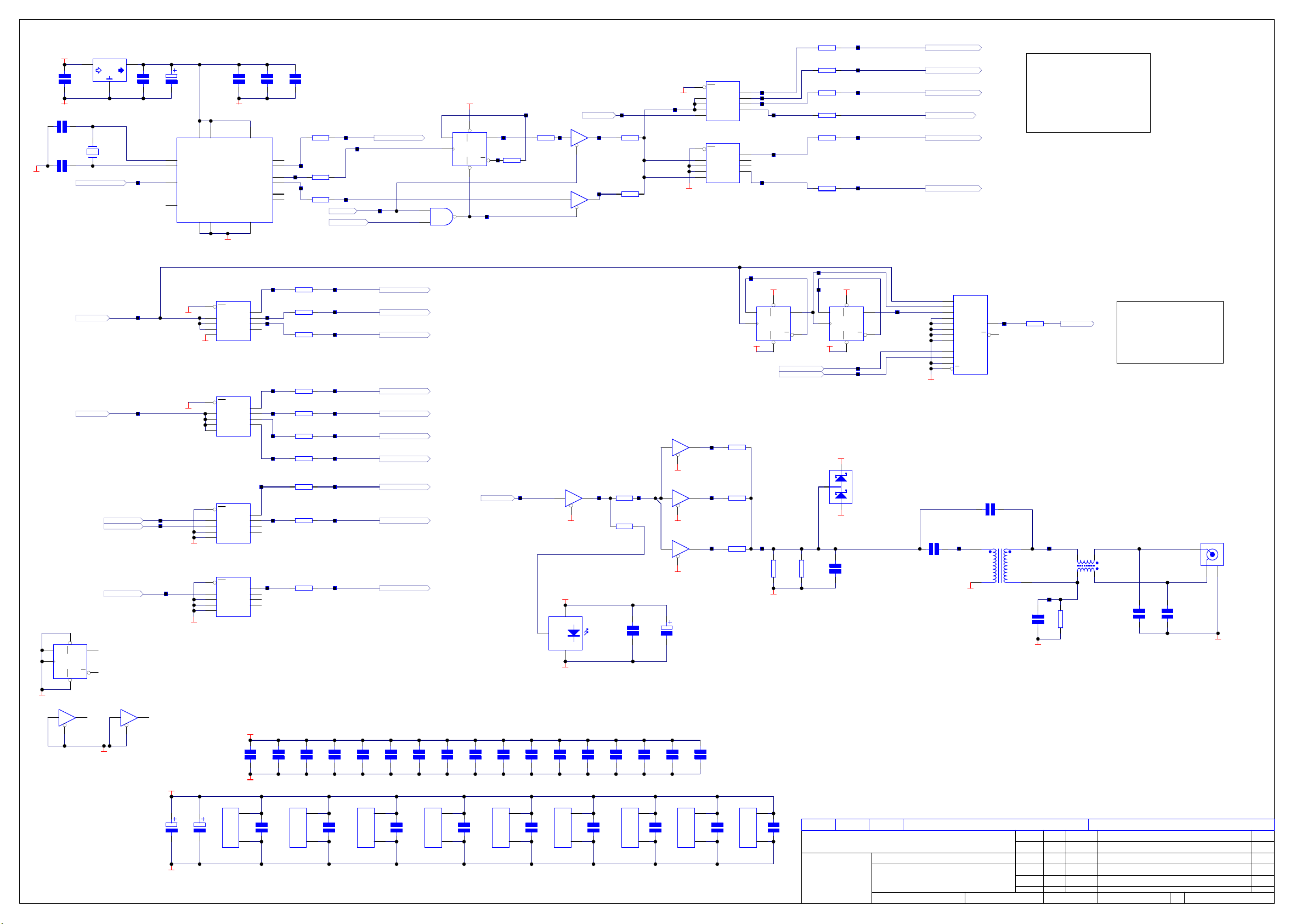
others 1 1 OFF
C302
100N
16V
0603
REG300
LM1086CS-3.3
TO-263
FSEL0
X300
27MHz
HC49
+3V3
P302
C342
100N
16V
0603
7
8
14
16
+3V3PLL
C303
100UF
10V
YXF
XTI
XTO
FSEL
NC
+5VD
DGND DGND
C300
27P
100V
0805
C301
DGND
27P
100V
0805
CLOCK GENERATOR
C306
100N
16V
0603
DGND
5
VDD2
MO1
MO2
AO1
AO2
SO1
SO2
VSS2
6
1
2
VDD312VDD1
IC300
SM8707E
VSOP-16
VSS311VSS1
C311
100N
16V
0603
3
4
9
10
13
15
C308
100N
16V
0603
R300
75R 0603
P341
R301
P340
100R 0603
P342
R306
100R
0603
P343
P344
FSEL1
ENABLE_AV
P345
27MHz
CLK27M_VADDIS
P346
CLOCK DIVIDER
+3V3D
12
D
11
CLK
1
4
2
IC303A
SN74AHC1G00DBVR
DBV-5
P356
10
IC306B
9
P349
Q
SD
P348
R323
8
Q
RD
13
100R 0603
74LVC74AD
S0-14
P347
Ensures audio clock can be trurned off in standby mode
R308
100R 0603
P357
9 8
12 11
AUDIO CLOCK BUFFER
IC301A
1
OE
DGND
2
A0
4
A1
6
P360
A2
8
A3
74LVC244APW
TSSOP-20
IC301B
19
OE
17
A0
15
A1
13
A2
11
A3
74LVC244APW
DGND
TSSOP-20
Spare clock buffer used to buffer mute control
P358
P359
P350
R309
100R
0603
R322
100R 0603
MUTE* MUTE_BUF*
IC307C
10
74LVC125AD
SO-14
IC307D
74LVC125ADSO-14
13
18
Y0
Y1
Y2
Y3
Y0
Y1
Y2
Y3
P318
16
P319
14
P320
12
3
5
7
9
P323
P300
P321
R302
100R 0603
R303
100R 0603
R304
100R 0603
R305
1K8 0603
R310
100R 0603
R307
100R 0603
P325
P326
P327
Base resistor for TR401 here to reduce noise on MUTE_BUF*
P301
P329
PSU CLOCK DIVIDER
MCLK_DAC0
MCLK_DAC1
MCLK_DAC2
MCLK_VADDIS
MCLK_HDMI
Audio master clock frequency for different sample
rates
Fs Master clock frequency
FSEL1..0
44.1kHz 11.2896MHz (256 x Fs) 00
48kHz 12.288MHz (256 x Fs) 01
88.2kHz 22.5792MHz (256 x Fs) 10
96kHz 24.576MHz (256 x Fs) 11
176.4kHz 22.5792MHz (128 x Fs) 10
192kHz 24.576MHz (128 x Fs) 11
DGND
2
D
3
CLK
2 3
4
SD
RD
74LVC74AD
1
S0-14
IC307A
1
74LVC125AD
SO-14
ALRCLK
ABCLK
IC306A
5
Q
6
Q
DGND
ADAT0
ADAT1
ADAT2
5 6
P334
P335
IC307B
4
74LVC125AD
SO-14
P361
P364
P365
+3V3D
DGND
DGND
DGND
C305
100UF
10V
YXF
DGND
DGND
DGND
I2S BUFFER
IC302A
1
OE
2
A0
4
A1
6
A2
8
A3
74LVC244APW
TSSOP-20
IC302B
19
OE
17
A0
15
A1
13
A2
11
A3
74LVC244APW
TSSOP-20
IC309A
1
OE
2
A0
4
A1
6
A2
8
A3
74LVC244APW
TSSOP-20
IC309B
19
OE
17
A0
15
A1
13
A2
11
A3
74LVC244APW
TSSOP-20
IC307E
VCC
C307
100UF
10V
GND
YXF
74LVC125AD
SO-14
Y0
Y1
Y2
Y3
Y0
Y1
Y2
Y3
Y0
Y1
Y2
Y3
Y0
Y1
Y2
Y3
+3V3D
DGND
14
7
18
16
14
12
3
5
7
9
18
16
14
12
3
5
7
9
C325
100N
16V
0603
P366
C317
100N
16V
0603
P311
P312
P313
P305
P306
P307
P368
P371
RP301A
1 8
100R 1206
RP301B
2 7
100R 1206
RP301C
100R 1206
RP300A
1 8
100R 1206
RP300B
2 7
100R 1206
RP300C
100R 1206
R313
56R
0W125 0805
RP302A
1 8
100R 1206
RP302C
100R 1206
R312
100R 0603
C326
100N
16V
0603
IC301C
VCC
GND
74LVC244APW
TSSOP-20
20
10
63
63
63
C327
100N
16V
0603
P314
P315
P316
P308
P309
P310
P317P303
C309
100N
16V
0603
P372
P374
P376
C328
100N
16V
0603
C329
100N
16V
0603
IC302C
20
VCC
10
GND
74LVC244APW
TSSOP-20
ALRCLK_DAC0
ALRCLK_DAC1
ALRCLK_DAC2
ABCLK_DAC0
ABCLK_DAC1
ABCLK_DAC2
ABCLK_HDMI
ADAT_DAC0
ADAT_DAC1
ADAT_DAC2
C330
100N
16V
0603
C310
100N
16V
0603
C331
100N
16V
0603
IC309C
20
VCC
10
GND
74LVC244APW
TSSOP-20
C332
100N
16V
0603
C318
100N
16V
0603
C333
100N
16V
0603
SPDIF
C334
100N
16V
0603
IC304C
VCC
GND
74LVC74AD
S0-14
IC304A
5
6
P352
P353
12
11
+3V3D
D
CLK
+3V3D
10
13
Q
SD
Q
RD
74LVC74AD
S0-14
P362
P363
IC304B
9
8
P354
PSUFS0
PSUFS1
DGND
4
3
2
1
15
14
13
12
11
10
9
7
IC305A
I0
I1
I2
I3
I4
I5
I6
I7
S0
S1
S2
E
74HC151D
SO-16
PSUCLK SHOULD BE 44.1kHz OR 48kHz
Fs PSUFS1 PSUFS0 PSUCLK
44.1kHz 0 0 44.1kHz
48kHz 0 0 48kHz
88.2kHz 0 1 44.1kHz
96kHz 0 1 48kHz
176.4kHz 1 0 44.1kHz
192kHz 1 0 48kHz
P355
R311
100R 0603
PSUCLK
5
Y
6
Y
P351
2
3
+3V3D
D
CLK
+3V3D
4
1
Q
SD
Q
RD
74LVC74AD
S0-14
PSUFS0
PSUFS1
SPDIF COAX OUTPUT
IC308B
5 6
74LVC125AD
4
SO-14
DGND
5
3
C339
100N
16V
0603
IC308C
9 8
74LVC125AD
10
SO-14
IC308D
12 11
74LVC125AD
13
SO-14
DGND
C304
100UF
10V
YXF
C340
100N
16V
0603
IC308E
VCC
C319
100N
16V
GND
0603
74LVC125AD
SO-14
P324
14
7
IC308A
2 3
74LVC125AD
1
SO-14
DGND DGND
SPDIF_OP
+5VD
2
VCC
1
I/P
GND
3
DGND
C335
C336
100N
100N
16V
16V
0603
0603
IC305B
16
VCC
C312
100N
16V
0603
GND
74HC151D
SO-16
8
R314
P328 P330
100R 0603
R321
100R 0603
OPTICAL OUT
TX300
JFJ1001-010010
C337
C338
100N
100N
16V
16V
0603
0603
VCC
C313
100N
16V
GND
0603
IC303B
SN74AHC1G00DBVR
DBV-5
C314
100N
50V
0805
R315
P322
750R 0603
R316
P331
750R 0603
R317
P332 P333 P337
750R 0603
C341
100N
16V
0603
C320
100N
16V
0603
IC306C
74LVC74AD
S0-14
14
7
VCC
GND
R318
120R
0W125
0805
DGND
14
C324
100N
16V
7
0603
+3V3D
D300
BAT54S
SOT-23
DGND
C343
R319
1K0
0W125
0805
ITEM300 1 Pad Damping 7.5x6x3MM RubberE828AP Fit on one side of X300 (see assembly drawing)
DRAWING TITLE
A & R Cambridge Ltd.
Pembroke Avenue
Waterbeach
Cambridge CB5 9QR
C321
47P
100V
0805
NF
DV79 MAIN CLOCKS & SPDIF
Filename:
Notes:
Contact Engineer:
100N 50V
0805
NF
Transformer is option for digital output
L967C3.Sch
DGND
Contact Tel: (01223) 203270Peter Gaggs
C315
100N 50V
0805
TX301
PCB Mount SMT
Schott / 37211
NF
P304
51
84
P336
C316
NF
100N
50V
0805
DGND
PG 1.003_E020 19-02-04 Production release
ECO No. DESCRIPTION OF CHANGE
INITIALS
Printed:
R320
0R0
0W125
0805
19-Feb-2004
2
3
DATE
1
L301
1000R @ 100MHz
4
DLW31S
3 11Sheet of
C322
100P
100V
0805
NF
SPDIF_OUT
SPDIF_GND
C323
10N
50V
0603
A2
SKT300
KUNMING
GOLD
EMC_GND
DRAWING NO.
SCRN
ISSUE
L967C3
Page 18
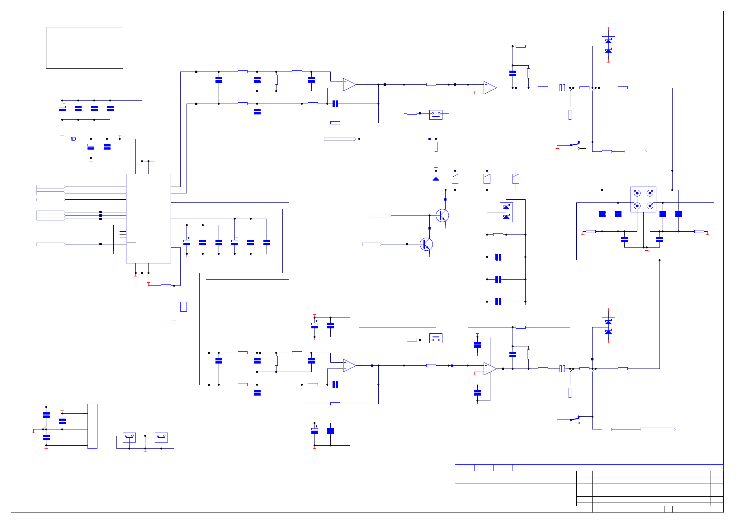
DGND
Audio outputs are inverted so as to be compatible with
DV88. This is compenstaed for in software by setting a
register in the DAC to invert the signal
+5VA
C400
C406
10UF
100N
35V
50V
SGET
0805
DGND
+3V3A
L400
DGND
ALRCLK_DAC0
ADAT_DAC0
ABCLK_DAC0
MCLK_DAC0
MD
MC
ML_8740_0
RESET*
IC402E
13
V+
12
VL
5
GND
4
V-
DG413DY
SO-16
C402
10UF
35V
SGET
+3V3_DAC0
ALRCLK_DAC0
ADAT_DAC0
ABCLK_DAC0
MCLK_DAC0
MD
MC
ML_8740_0
RESET*
+12VA
C421
100N
50V
0805
C422
100N
50V
0805
-12VA
120R@100MHz
+5VA
C423
100N
50V
0805
C407
100N
50V
0805
P400
P401
P438
P402
C408
100N
50V
0805
+3V3_DAC0
C414
100N
50V
0805
DGND
1
LRCKIN
2
DIN
3
BCKIN
5
SCLK
26
MD/DM0
27
MC/DM1
28
ML/I2S
23
CSBIOW
24
MODE
4
MODE8X
6
DIFFHW
25
MUTEB
22
RSTB
IC402C
DG413DY
SO-16
9
8
7
DGND
15
DVDD
DGND
14
+3V3_DAC0
1011
DGND
AVDD
AGND
DAC
20
AVDDL
AGNDL
19
9
AVDDR
VOUTL+
VOUTL-
VOUTR+
VOUTR-
VMIDL
VMIDR
ZERO
AGNDR
XWM8740EDS
10
SSOP-28
R416
10K
0W125
0805
NF
IC402D
DG413DY
SO-16
16
IC403
17
16
12
13
18
11
C403
10UF
21
35V
SGET
DGND
CON400
1
2
HARWIN
M20-973
DGND
NF
Useful for drop-out test
1415
P408
P409
C415
100N
50V
0805
P415
P416
C424
47P
100V
0805
C412
100N
100V
MKS2
C425
47P
100V
0805
R400
3K3
0W125
0805
R401
3K3
0W125
0805
C404
10UF
35V
SGET
R404
3K3
0W125
0805
R405
3K3
0W125
0805
FILTER
2nd order Bessel filter, Av=1
C426
R402
2N2
3K3
100V
0W125
FKP2
0805
DGND
C427
2N2
100V
FKP2
DGND
C416
C413
100N
100N
50V
100V
0805
MKS2
2nd order Bessel filter, Av=1
P417
C428
R406
2N2
3K3
100V
0W125
FKP2
0805
DGND
C429
2N2
100V
FKP2
DGND
R408
680R
0W125
0805
R410
680R
0W125
0805
DGND
R409
680R
0W125
0805
+12VA
DGND
R411
680R
0W125
0805
-12VA
C430
680P
100V
FKP2
C432
680P
100V
FKP2
C401
10UF
35V
SGET
C405
10UF
35V
SGET
5
6
C431
680P
100V
FKP2
R403
3K3
0W125
0805
GAIN_SCALING
1=HDCD gain, 0=normal
C409
100N
50V
0805
3
2
C433
680P
100V
FKP2
R407
3K3
0W125
0805
C417
100N
50V
0805
84
IC400B
7
OPA2134UA
SO-8
AC_PRES*
IC400A
1
OPA2134UA
SO-8
MUTE_BUF*
P421
P414
GAIN_SCALING
MUTING
MUTE_BUF*
AC_PRES*
Base resistor on PSU
R413
10K
0W125
0805
IC402B
DG413DY
P422
P428
SO-16
P431
P436
DGND
2 3
IC402A
DG413DY
SO-16
R418
10K
0W125
0805
R412
10K
0W125
0805
Base resistor on sheet 3
P435
R417
10K
0W125
0805
8
DGND
+5VD
TR400
BC849B
SOT-23
1
R415
10K
0W125
0805
D404
BAS16
SOT-323
DGND
OUTPUT BUFFER
Gain of -2.2 for HDCD, otherwise -1.1
Cheapo version could have bipolar op-amp, but without feedback round coupling cap
IC401B
6
5
OPA2134UA
SO-8
RLY500C
NEC
EB2-5NU
R436
100R
0W125
0805
C441
1N0
100V
0805
C442
1N0
100V
0805
C443
DGND EMC_GND
1N0
100V
0805
C410
100N
50V
0805
IC401A
84
2
3
OPA2134UA
SO-8
C411
100N
50V
0805
67
P437
TR401
FMMT497
SOT-23
P429
P423
RLY400C
NEC
EB2-5NU
DGND
+12VA
DGND
DGND
DGND
-12VA
R420
11K
0W125
0805
C434
33P
100V
0805
P424 P427
7
RLY600C
NEC
EB2-5NU
D401
BAT54S
SOT-23
R421
11K
0W125
0805
C435
33P
100V
0805
P430
1
R422
1M0
0W125
0805
R423
1M0
0W125
0805
R424
47R
0W125
0805
R426
47R
0W125
0805
DGND
DGND
C436
100UF
16V
NONP
C437
100UF
16V
NONP
+12VA
D400
BAT54S
SOT-23
-12VA
DGND
R414
47K
0W125
0805
RLY400A
NEC
EB2-5NU
R425
47R
0W125
0805
R434
1K0
0W125
0805
R428
0R0 0W 125
0805
LEFT_OUT
SCART_LEFT
LEFT
SKT400
KUNMING GOLD
OUT_GND1OUT_GND2
C444
1N0
100V
0805
C439
100P
100V
0805
C438
C418
100P
100P
100V
100V
0805
+12VA
-12VA
0805
D403
BAT54S
SOT-23
R430
0R0 0W 125
0805
R429
0R0
DGND DGND
0805
P434
R427
47R
0W125
0805
R419
47K
0W125
0805
DGND
RLY400B
NEC
EB2-5NU
R435
1K0
0W125
0805
C440
1N0
100V
0805
SCRN
EMC_GND
RIGHT_OUT
SCART_RIGHT
C419
100P
100V
0805
R431
0R0
0805
RIGHT
ITEM400 1 Pad Damping 7.5x6x3MM RubberE828AP
DRAWING TITLE
A & R Cambridge Ltd.
Pembroke Avenue
Waterbeach
Cambridge CB5 9QR
DV79 MAIN DAC L & R AUDIO
Filename:
Notes:
Contact Engineer:
L967C4.Sch
Fit on top of RLY400
PG 1.003_E020 19-02-04 Production release
INITIALS
Printed:
DATE
19-Feb-2004
4 11Sheet of
A2
DRAWING NO.
Contact Tel: (01223) 203270Peter Gaggs
ECO No. DESCRIPTION OF CHANGE
ISSUE
L967C4
Page 19
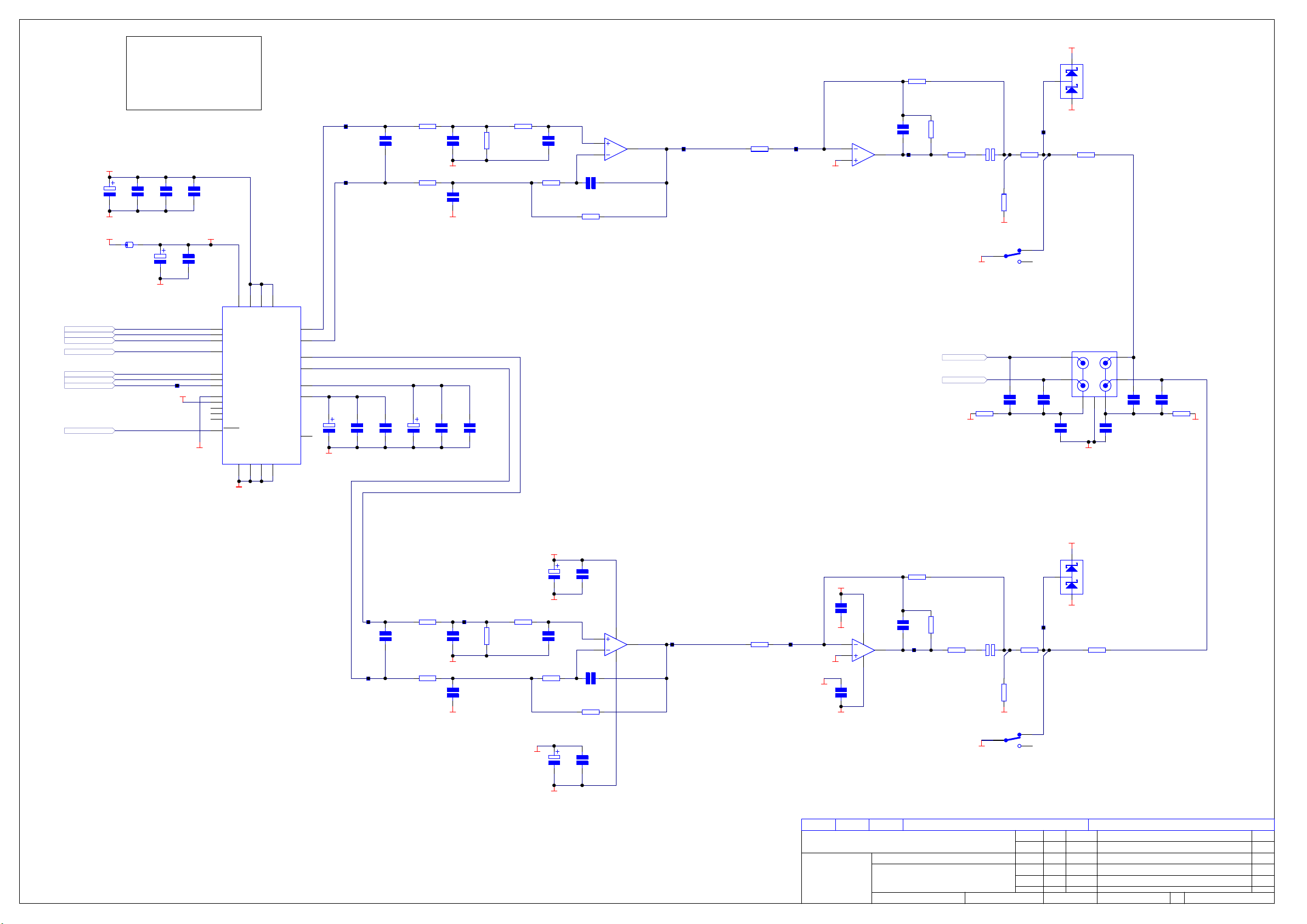
ALRCLK_DAC1
ADAT_DAC1
ABCLK_DAC1
MCLK_DAC1
MD
MC
ML_8740_1
RESET*
Audio outputs are inverted so as to be compatible with
DV88. This is compenstaed for in software by setting a
register in the DAC to invert the signal
+5VA
C500
C506
100N
50V
0805
DGND
C507
100N
50V
0805
C502
10UF
35V
SGET
P531
+3V3_DAC1
10UF
35V
SGET
DGND
+3V3A
120R@100MHz
L500
ALRCLK_DAC1
ADAT_DAC1
ABCLK_DAC1
MCLK_DAC1
MD
MC
ML_8740_1
RESET*
C508
100N
50V
0805
+3V3_DAC1
C514
100N
50V
0805
DGND
26
27
28
23
24
25
22
1
2
3
5
4
6
LRCKIN
DIN
BCKIN
SCLK
MD/DM0
MC/DM1
ML/I2S
CSBIOW
MODE
MODE8X
DIFFHW
MUTEB
RSTB
DGND
P518
C535
470P
100V
0805
+12VA
D500
BAT54S
SOT-23
-12VA
R524
0R0
0805
SKT500
KUNMING GOLD
C536
1N0
100V
0805
EMC_GND
LS_OUT
LEFT SURR
RIGHT SURR
C519
470P 100V
C518
0805
470P
100V
C537
1N0
100V
0805
0805
OUT_GND3OUT_GND4
SCRN
0R0
0805
R527
OUTPUT BUFFER
Gain of -1.1
Cheapo version could have bipolar op-amp, but without feedback round coupling cap
FILTER
P507
P508
C520
47P
100V
0805
R500
3K3
0W125
0805
R501
3K3
0W125
0805
2nd order Bessel filter, Av=1
C522
R502
2N2
3K3
100V
0W125
FKP2
0805
DGND
C523
2N2
100V
FKP2
DGND
R508
680R
0W125
0805
R509
680R
0W125
0805
C526
680P
100V
FKP2
C527
680P
100V
FKP2
R503
3K3
0W125
0805
IC500B
5
7
6
OPA2134UA
SO-8
P513 P514
R512
10K
0W125
0805
DGND
IC501B
6
5
OPA2134UA
SO-8
DAC
9
20
15
8
AVDD
DVDD
AVDDL
DGND
AGNDL
AGND
7
14
19
AVDDR
AGNDR
10
VOUTL+
VOUTL-
VOUTR+
VOUTR-
VMIDL
VMIDR
ZERO
IC502
17
16
12
13
18
11
21
DGND
XWM8740EDS
SSOP-28
C503
10UF
35V
SGET
C515
100N
50V
0805
C512
100N
100V
MKS2
C504
10UF
35V
SGET
C516
100N
50V
0805
C513
100N
100V
MKS2
R516
11K
0W125
0805
R518
C530
1M0
33P
0W125
100V
0805
0805
P515
7
R520
47R
0W125
0805
DGND
C532
100UF
16V
NONP
DGND
R513
47K
0W125
0805
RLY500B
NEC
EB2-5NU
R521
47R
0W125
0805
CENTRE
0R0
0805
CENTRE_OUT
SUB_OUT
C534
470P
100V0805
CENTRE_OUT
From sheet 6
SUB_OUT
SUB
R525
DGND DGND
P520
P519
C521
47P
100V
0805
R504
3K3
0W125
0805
R505
3K3
0W125
0805
2nd order Bessel filter, Av=1
P521
C524
R506
2N2
3K3
100V
0W125
FKP2
0805
DGND
C525
2N2
100V
FKP2
DGND
R510
680R
0W125
0805
DGND
+12VA
DGND
R511
680R
0W125
0805
-12VA
C528
680P
100V
FKP2
C501
10UF
35V
SGET
C505
10UF
35V
SGET
C509
100N
50V
0805
C529
680P
100V
FKP2
R507
3K3
0W125
0805
C517
100N
50V
0805
+12VA
-12VA
19-Feb-2004
D501
BAT54S
SOT-23
R526
0R0 0W 125
0805
Fit on top of RLY500
DATE
5 11Sheet of
RS_OUT
A2
DRAWING NO.
ISSUE
L967C5
R517
+12VA
C510
100N
50V
0805
IC500A
84
3
1
2
OPA2134UA
SO-8
P525 P526
R514
10K
0W125
0805
DGND
DGND
DGND
-12VA
ITEM500 1 Pad Damping 7.5x6x3MM RubberE828AP
DRAWING TITLE
A & R Cambridge Ltd.
Pembroke Avenue
Waterbeach
Cambridge CB5 9QR
IC501A
84
2
3
OPA2134UA
SO-8
C511
100N
50V
0805
DV79 MAIN DAC LS & RS AUDIO
Filename:
Notes:
Contact Engineer:
11K
0W125
0805
R519
C531
1M0
33P
0W125
100V
0805
0805
1
P527
L967C5.Sch
R522
47R
0W125
0805
C533
100UF
16V
NONP
R515
47K
0W125
0805
DGND
RLY500A
DGND
NEC
EB2-5NU
Contact Tel: (01223) 203270Peter Gaggs
P530
R523
47R
0W125
0805
PG 1.003_E020 19-02-04 Production release
ECO No. DESCRIPTION OF CHANGE
INITIALS
Printed:
Page 20
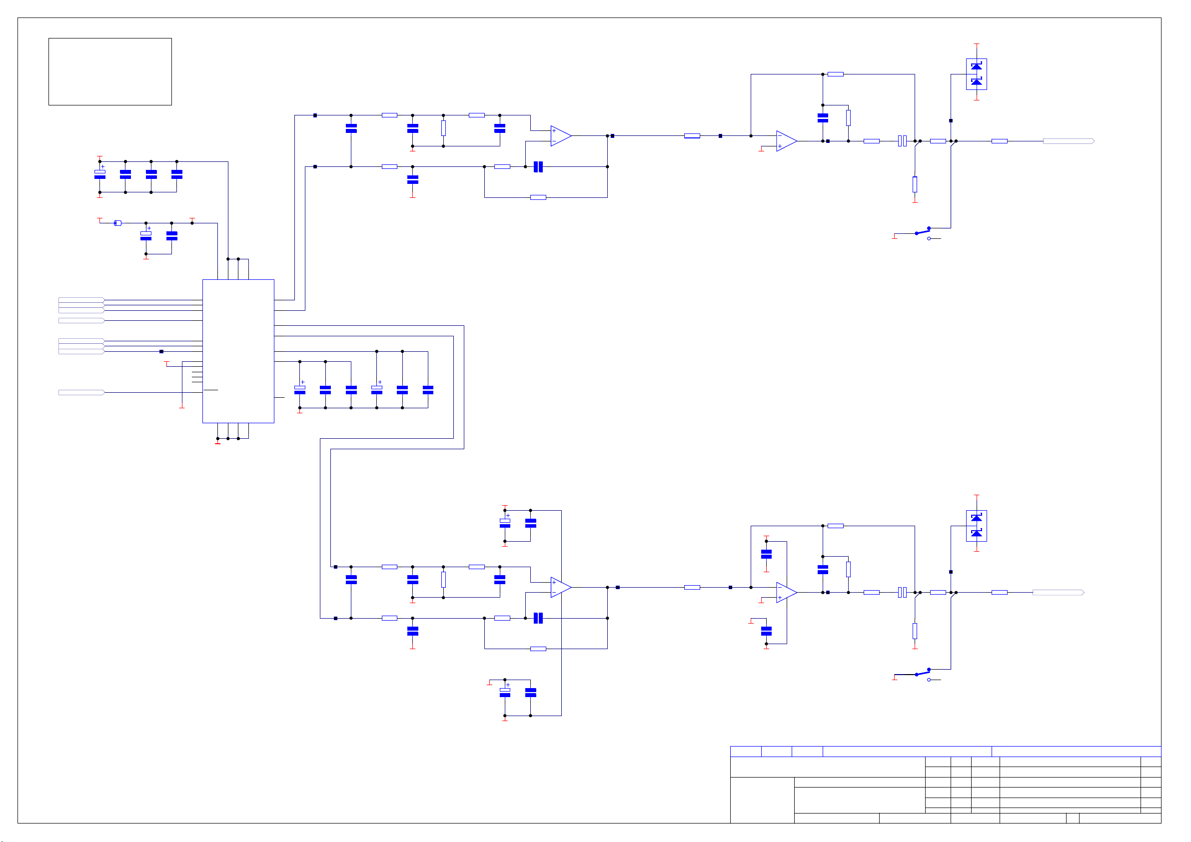
Audio outputs are inverted so as to be compatible with
DV88. This is compenstaed for in software by setting a
register in the DAC to invert the signal
+5VA
C600
C606
10UF
100N
35V
50V
SGET
0805
DGND
+3V3A
L600
DGND
ALRCLK_DAC2
ADAT_DAC2
ABCLK_DAC2
MCLK_DAC2
MD
MC
ML_8740_2
RESET*
C602
10UF
35V
SGET
+3V3_DAC2
ALRCLK_DAC2
ADAT_DAC2
ABCLK_DAC2
MCLK_DAC2
MD
MC
ML_8740_2
RESET*
120R@100MHz
C607
100N
50V
0805
P631
C608
100N
50V
0805
+3V3_DAC2
C614
100N
50V
0805
DGND
26
27
28
23
24
25
22
1
2
3
5
4
6
LRCKIN
DIN
BCKIN
SCLK
MD/DM0
MC/DM1
ML/I2S
CSBIOW
MODE
MODE8X
DIFFHW
MUTEB
RSTB
DGND
P618
+12VA
-12VA
D600
BAT54S
SOT-23
R624
0R0 0W 125
0805
Connector on sheet 5
CENTRE_OUT
OUTPUT BUFFER
Gain of -1.1
Cheapo version could have bipolar op-amp, but without feedback round coupling cap
FILTER
P607
P608
C620
47P
100V
0805
R600
3K3
0W125
0805
R601
3K3
0W125
0805
2nd order Bessel filter, Av=1
C622
R602
2N2
3K3
100V
0W125
FKP2
0805
DGND
C623
2N2
100V
FKP2
DGND
R608
680R
0W125
0805
R609
680R
0W125
0805
C626
680P
100V
FKP2
C627
680P
100V
FKP2
R603
3K3
0W125
0805
IC600B
5
7
6
OPA2134UA
SO-8
P613 P614
R612
10K
0W125
0805
DGND
IC601B
6
5
OPA2134UA
SO-8
DAC
9
20
15
8
AVDD
DVDD
AVDDL
DGND
AGNDL
AGND
7
14
19
AVDDR
AGNDR
10
VOUTL+
VOUTL-
VOUTR+
VOUTR-
VMIDL
VMIDR
ZERO
IC602
17
16
12
13
18
11
21
DGND
XWM8740EDS
SSOP-28
C603
10UF
35V
SGET
C615
100N
50V
0805
C612
100N
100V
MKS2
C604
10UF
35V
SGET
C616
100N
50V
0805
C613
100N
100V
MKS2
R616
11K
0W125
0805
R618
C630
1M0
33P
0W125
100V
0805
0805
P615
7
R620
47R
0W125
0805
DGND
C632
100UF
16V
NONP
DGND
R613
47K
0W125
0805
RLY600B
NEC
EB2-5NU
R621
47R
0W125
0805
P620
P619
C621
47P
100V
0805
R604
3K3
0W125
0805
R605
3K3
0W125
0805
2nd order Bessel filter, Av=1
C624
R606
2N2
3K3
100V
0W125
FKP2
0805
DGND
C625
2N2
100V
FKP2
DGND
R610
680R
0W125
0805
DGND
+12VA
DGND
R611
680R
0W125
0805
-12VA
C628
680P
100V
FKP2
C601
10UF
35V
SGET
C605
10UF
35V
SGET
C609
100N
50V
0805
C629
680P
100V
FKP2
R607
3K3
0W125
0805
C617
100N
50V
0805
+12VA
-12VA
19-Feb-2004
D601
BAT54S
SOT-23
R626
0R0 0W 125
0805
Fit on top of RLY600
DATE
Connector on sheet 5
SUB_OUT
6 11Sheet of
A2
DRAWING NO.
ISSUE
L967C6
R617
+12VA
C610
100N
50V
0805
IC600A
84
3
1
2
OPA2134UA
SO-8
P625 P626
R614
10K
0W125
0805
DGND
DGND
DGND
-12VA
ITEM600 1 Pad Damping 7.5x6x3MM RubberE828AP
DRAWING TITLE
A & R Cambridge Ltd.
Pembroke Avenue
Waterbeach
Cambridge CB5 9QR
IC601A
84
2
3
OPA2134UA
SO-8
C611
100N
50V
0805
DV79 MAIN DAC CENTRE & SUB
Filename:
Notes:
Contact Engineer:
11K
0W125
0805
R619
C631
1M0
33P
0W125
100V
0805
0805
P627
1
L967C6.Sch
R622
47R
0W125
0805
C633
100UF
16V
NONP
R615
47K
0W125
0805
DGND
RLY600A
DGND
NEC
EB2-5NU
Contact Tel: (01223) 203270Peter Gaggs
P630
R623
47R
0W125
0805
PG 1.003_E020 19-02-04 Production release
ECO No. DESCRIPTION OF CHANGE
INITIALS
Printed:
Page 21
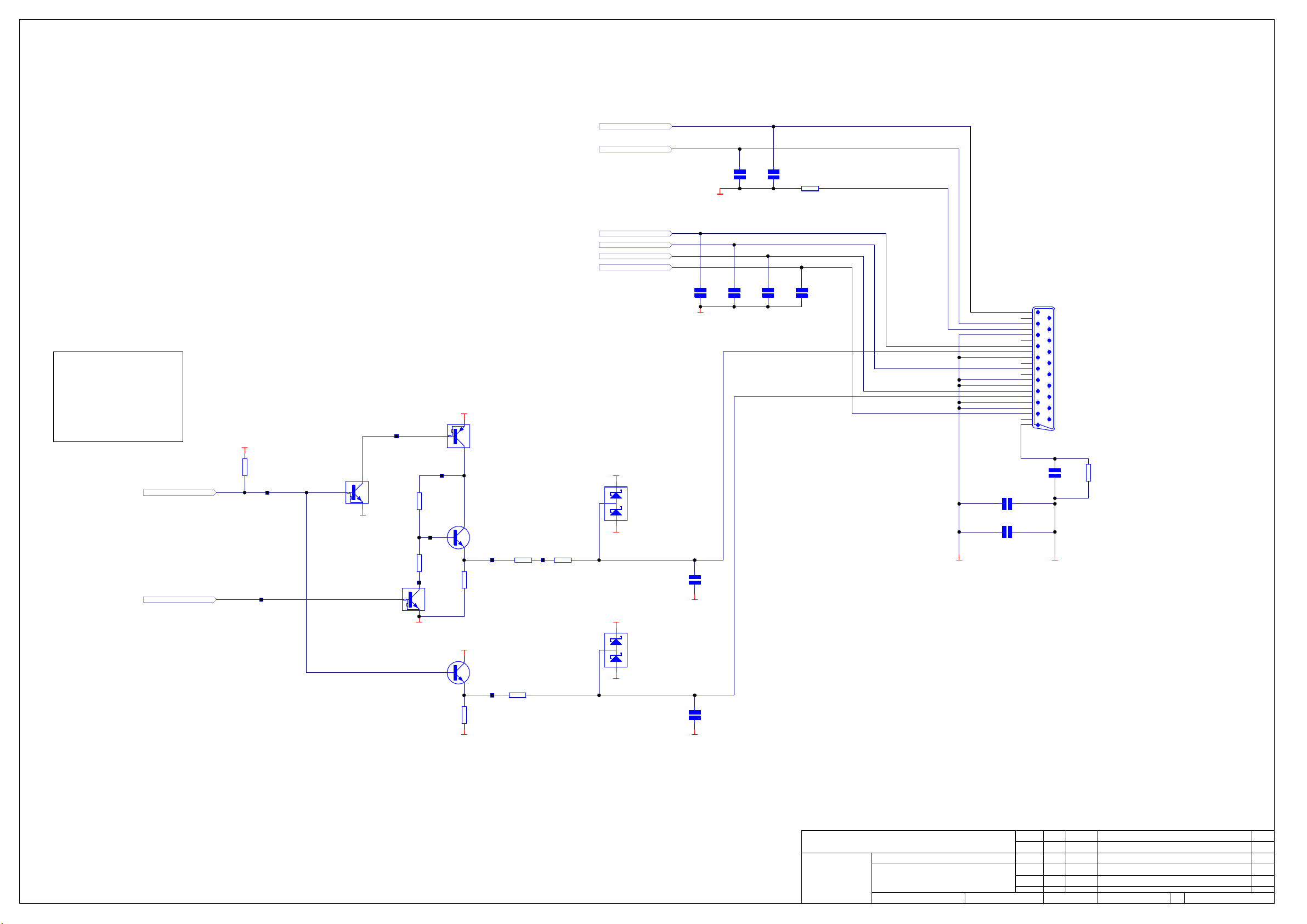
AUDIO
SCART_RIGHT
SCART_LEFT
SCART control signals
ENABLE_AV: 0 in when standby mode, 1 when on
(3V3 levels)
(RGB_STAT is supposed to be >1V when driving 75R)
16/9: 0 when 4:3 output, 1 when 16:9 output (3V3
levels)
0/6/12: 0V in standby, 6V when output is 16:9, 12V
when output is 4:3
ENABLE_AV
CONTROL
16/9
+5V_VID
R801
1K0
0W125
0805
P810
P811
DGND
P812
TR801
MMUN2211LT1
SOT-23
R807
4K7
0W125
0805
R806
6K8
0W125
0805
P814
TR802
MMUN2211LT1
SOT-23
DGND
P815
P816
+12VD
+5V_VID
DGND
TR800
MMUN2111LT1
SOT-23
TR803
BC849B
SOT-23
P817 P818
R808
10K
0W125
0805
TR804
BC849B
SOT-23
P819
R811
1K0
0W125
0805
R809
330R
0W125
0805
R812
82R
0W125
0805
VIDEO
R810
330R
0W125
0805
RGB_STAT
SCART_BLUE
SCART_GREEN
SCART_RED
SCART_COMPOSITE
+12VD
D800
BAT54S
SOT-23
DGND
0/6/12
+5V_VID
D801
BAT54S
SOT-23
DGND
DGND
DGND
DGND
C806
100N
50V
0805
C807
100N
50V
0805
C802
47P
100V
0805
DGND
C803
47P
100V
0805
C800
47P
100V
0805
C804
47P
100V
0805
C801
47P
100V
0805
R800
0R0
0W125
0805
C805
47P
100V
0805
SCART OUTPUT
10
11
12
13
14
15
16
17
18
19
20
21
1
2
3
4
5
6
7
8
9
SKT800
CHARM
CW
SCART_RIGHT
SCART_LEFT
SCART_AGND
SCART_BLUE
0/6/12
SCART_GREEN
SCART_RED
RGB_STAT
SCART_COMPOSITE
C811
1N0 100V 0805
C812
1N0 100V 0805
DGND EMC_GND
C813
10N
50V
0603
R803
100R
0W125
0805
DRAWING TITLE
A & R Cambridge Ltd.
Pembroke Avenue
Waterbeach
Cambridge CB5 9QR
DV79 MAIN SCART OUTPUT
Filename:
L967C8.Sch
Notes:
Contact Engineer:
Contact Tel: (01223) 203270Peter Gaggs
PG 1.003_E020 19-02-04 Production release
INITIALS
Printed:
DATE
19-Feb-2004
8 11Sheet of
ECO No. DESCRIPTION OF CHANGE
A2
DRAWING NO.
ISSUE
L967C8
Page 22
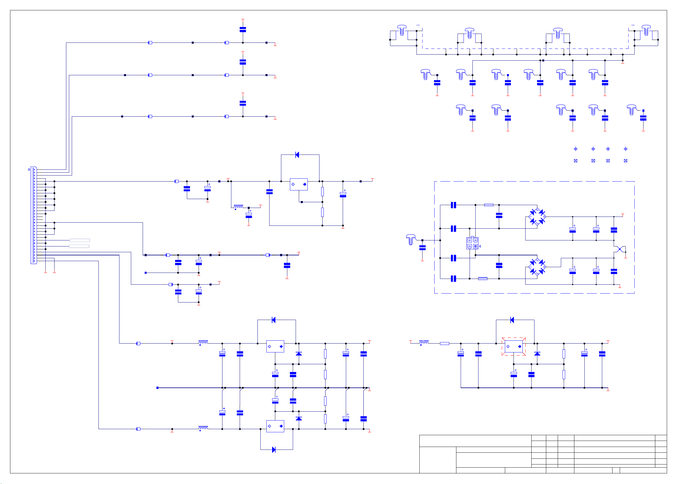
POWER IN
CON1001
1
2
3
4
5
6
7
8
9
10
11
12
13
14
15
16
17
18
19
20
21
22
23
24
25
26
27
28
29
30
31
32
MOLEX
52045
DGND DGND
-19V_IN
Spare
Spare
-9V_IN
-13V5_IN
+3V3D_IN
+5VD_IN
PSUCLK
AC_PRES*
+12VD_IN
+15V5_IN
-15V5_IN
PSUCLK
AC_PRES*
DGND
L1011
33U
1.17A
8RHT2
DGND
DGND
C1008
100N
50V
0805
C1006
100N
50V
0805
C1007
100N
50V
0805
For DACs
P1025
DGND
C1003
100N
50V
0805
C1005
100N
50V
0805
C1018
100UF
10V
YXF
+3V3A
DISPLAY BOARD SUPPLIES
L1006
120R@100MHz
Place these near power input
P1001 P1005
P1012
70R@100MHz
70R@100MHz
L1004
120R@100MHz
L1005
120R@100MHz
L1001
70R@100MHz
P1000 P1002
P1018
L1002
L1003
L1000
70R@100MHz
L1012
120R@100MHz
+15V5
P1019
-15V5
P1024
-19V
P1022
-9V
P1023
-13V5
C1001
100N
50V
0805
DGND
DGND
DGND
33U
1.17A
8RHT2
33U
1.17A
8RHT2
L1013
L1015
C1010
100UF
25V
YK
C1031
100UF
25V
YK
C1000
100N
50V
0805
C1030
100N
50V
0805
Have made C1039, C1040 & C1041 12.5mm di a for flexibili ty
P1021
C1011
100UF
25V
YK
+5VD
+12VD
L1009
120R@100MHz
L1007
120R@100MHz
L1008
120R@100MHz
+3V3D
P1003
C1039
100UF
50V
YXF
C1041
100UF
50V
YXF
P1007
-19V_OUT
-9V_OUT
P1006
-13V5_OUT
C1002
100N
50V
0805
L1010
120R@100MHz
D1001
S1D
DO-214AC (SMA)
REG1000
LM317T TO-220
ADJ
ADJ
REG1002
LM337T
TO-220
D1005
S1D
DO-214AC (SMA)
To display board
VADDIS +1.8V REGULATOR
D1000
S1D
DO-214AC (SMA)
REG1003
LM1086CS-ADJ
TO-263
R1000
120R
0W125
0805
R1006
56R
0W125
0805
P1008
DGND
ADJ
P1009
+5V_DISPLAY
C1009
100N
50V
0805
AUDIO SUPPLY REGULATORS
D1002
S1D
DO-214AC (SMA)
C1014
100UF
25V
YK
C1017
100UF
25V
YK
C1033
100N
100V
MKS2
C1035
100N
100V
MKS2
D1006
S1D
DO-214AC (SMA)
M3 R/A PCB FIXING BRACKETS
+1V8D
P1004
C1012
100UF
25V
YK
DGND
+12VA
R1001
390R
0W125
0805
R1004
3K3
0W125
0805
R1005
3K3
0W125
0805
R1003
390R
0W125
0805
Have made C1019 & C1021 footprints 12.5m m dia for flexibility
C1019
220UF
16V
YXF
C1021
220UF
16V
YXF
C1036
100N
100V
MKS2
DGND
C1038
100N
100V
MKS2
-12VA
ITEM1002
4
1
23
FIX1003
Dia 3.5mm
+15V5
SH1000
1
FIX1009
Dia 3.5mm
P1033
1
C1025
1N0
50V
0603
DGND
L1014
33U
1.17A
8RHT2
DRAWING TITLE
A & R Cambridge Ltd.
Pembroke Avenue
Waterbeach
Cambridge CB5 9QR
FIX1010
P1010
1
C1042
1N0
Dia 3.5mm
50V
0603
DGND
R1008
22R
0W25
MF
C1045
1N0
100V
0805
C1050
1N0
100V
0805
C1051
1N0
100V
0805
C1052
1N0
100V
0805
FIX1011
Dia 3.5mm
DV79 MAIN Power
Filename:
Notes:
Contact Engineer:
ITEM1004
4
ACIN1
ACIN2
ACIN4
C1040
100UF
50V
YXF
1
DGND
1
DGND
4
2
P1013
1
23
C1043
1N0
50V
0603
C1013
1N0
50V
0603
FS1000
T2A
R452
3
CON1002
MOLEX
44472
1
ACIN3
FS1001
T2A
R452
C1004
100N
50V
0805
L967C10.Sch
ITEM1005
4
EMC CAN
NOT FITTED
P1031
P1032
C1022
1N0
50V
0603
NF
C1023
1N0
50V
0603
NF
FIX1001
1
Dia 3.5mm
DGND
FIX1000
1
Dia 3.5mm
DGND
FIX1002
1
Dia 3.5mm
DGND
AUX PSU (NOT FITTED FOR DV79)
OPTION FOR FMJ
C1016
100N
50V
0805
C1044
100N
50V
0805
P1034
C1024
1N0
50V
0603
4mm tooling holes
DBR1000
W02G
DBR1001
W02G
NFNF
FIX1004
Dia 3.5mm
FIX1005
Dia 3.5mm
Fiducials
AUDIO DAC SUPPLY
D1003
S1D
DO-214AC (SMA)
REG1001
LM317T TO-220
HS1000A
6043PB
23C/W
NF
Contact Tel: (01223) 203270Peter Gaggs
ADJ
C1015
100UF
25V
YK
D1004
S1D
DO-214AC (SMA)
C1034
100N
100V
MKS2
PG 1.003_E020 19-02-04 Production release
ECO No. DESCRIPTION OF CHANGE
INITIALS
19-Feb-2004
Printed:
1
23
FIX1006
1
C1026
1N0
Dia 3.5mm
50V
0603
DATE
DGND
1
DGND
R1002
330R
0W125
0805
R1007
1K0
0W125
0805
FIX1007
P1035 P1036 P1037
C1027
1N0
Dia 3.5mm
50V
0603
TOOL1000 TOOL1001
FD1000 FD1001
C1053
1000UF
35V
YK
C1054
1000UF
35V
YK
C1020
470UF
25V
YXF
Keep large footprint for C1020 C POL/RB12.5X25/5
10 11Sheet of
EMC_GND
1
C1028
1N0
50V
0603
DGND
1
C1029
1N0
50V
0603
DGND
TOOL1002 TOOL1003
FD1002 FD1003
C1048
3300UF
35V
YK
C1049
3300UF
35V
YK
+5VA
C1037
100N
100V
MKS2
DGND
A2
C1046
470N
100V
MKS2
SP1000
C1047
470N
100V
MKS2
-15V5
FIX1008
Dia 3.5mm
+15V5
DGND
DRAWING NO.
EMC Shield
ITEM1003
4
1
DGND
L967C10
C1032
1N0
50V
0603
NF
1
23
ISSUE
Page 23

Place resisors so as to get I2S signals close for when SiI9030 is used
+3V3D
DGND
+3V3D
DGND
ADAT0
ADAT1
ADAT2
ALRCLK
ABCLK_HDMI
C1134
100N
16V
0603
Around video bus
C1121
100UF
10V
YXF
C1135
100N
16V
0603
IC1100C
20
VCC
10
GND
74LVC244APW
TSSOP-20
1=Prog scan, 0=Interlaced
PROG/INT*
C1136
100N
16V
0603
C1111
100N
16V
0603
C1137
100N
16V
0603
IC1101C
74LVC244APW
TSSOP-20
33R 0603
33R 0603
33R 0603
33R 0603
33R 0603
VCC
GND
R1100
R1101
R1102
R1103
R1104
C1138
100N
16V
0603
NF
NF
NF
NF
NF
VIDEO BUSES
1. Progressive Mode: 10 Bit Y/C on 20 bit wide bus
DGND
20
10
Vaddis V Output Function SiI9190 Input
VIDP19..12 Y9..2 D15..8
VIDP11..10 Y1..0 D3..2
VIDP9..2 C9..2 D23..16
VIDP1..0 C1..0 D7..6
(C = multiplexed CbCr data)
2. Interlaced Mode: 8 Bit multiplexed YCbCr
Vaddis V Output Function SiI9190 Input
VIDP7..0 YC7..0 D15..8
VIDP[0..19]
P1130
P1131
+3V3D
DGND
C1112
100N
16V
0603
R1114
10K
0805
VIDP[0..19]
TR1102
MMUN2211LT1
SOT-23
VIDP7
VIDP6
VIDP5
VIDP4
VIDP19
VIDP18
VIDP17
VIDP16
VIDP3
VIDP2
VIDP1
VIDP0
VIDP15
VIDP14
VIDP13
VIDP12
IC1100A
1
OE
2
A0
4
A1
6
A2
8
A3
74LVC244APW
TSSOP-20
IC1100B
19
OE
17
A0
15
A1
13
A2
11
A3
74LVC244APW
TSSOP-20
IC1101A
1
OE
2
A0
4
A1
6
A2
8
A3
74LVC244APW
TSSOP-20
IC1101B
19
OE
17
A0
15
A1
13
A2
11
A3
74LVC244APW
TSSOP-20
18
Y0
16
Y1
14
Y2
12
Y3
3
Y0
5
Y1
7
Y2
9
Y3
18
Y0
16
Y1
14
Y2
12
Y3
3
Y0
5
Y1
7
Y2
9
Y3
+5VD
P1114
P1115
P1116
P1117
P1122
P1123
P1124
P1125
C1100
100N
16V
0603
RP1100A
RP1100B
RP1100C
RP1100D
RP1101A
RP1101B
RP1101C
RP1101D
REG1100
LM1086CS-3.3
TO-263
DGND
1 8
2 7
1 8
2 7
+3V3
+3V3D
L1100
120R@100MHz
NF
Option to bypass reg
100R
100R
100R
63
100R
54
100R
100R
100R
63
100R
54
+3V3_HDMI
C1116
10UF
50V
YK
9190_INT*
HD15
HD14
HD13
HD12
HD11
HD10
HD9
HD8
P1118
P1119
P1120
P1121
P1126
P1127
P1128
P1129
+3V3D
DGND
DGND
+3V3D
DGND
R1105
10K
0W125
0805
L1101
120R@100MHz
C1101
100N
16V
0603
L1102
120R@100MHz
C1102
100N
16V
0603
L1103
120R@100MHz
C1103
100N
16V
0603
HDMI_RESET*
3V3_PVCC2
3V3_PVCC1
3V3_AVCC
VSYNC*
HSYNC*
CLK27M_VID
MCLK_HDMI
SPDIF
P1133
P1132
SCL
SDA
CLK27M_VID
MCLK_HDMI
SPDIF
C1117
100UF
10V
YXF
C1118
100UF
10V
YXF
C1119
100UF
10V
YXF
HDMI_RESET*
9190_INT*
SCL
SDA
VIDP9
VIDP8
VIDP7
VIDP6
VIDP5
VIDP4
VIDP3
VIDP2
HD15
HD14
HD13
HD12
HD11
HD10
HD9
HD8
VIDP1
VIDP0
VIDP11
VIDP10
VSYNC*
HSYNC*
DGND
C1104
100N
16V
0603
C1105
100N
16V
0603
C1106
100N
16V
0603
C1122
1N0
50V
0603
C1123
1N0
50V
0603
C1107
100N
16V
0603
18
33
23
29
AVCC
RESET#
INT
SCL
SDA
D23
D22
D21
D20
D19
D18
D17
D16
D15
D14
D13
D12
D11
D10
D9
D8
D7
D6
D5
D4
D3
D2
D1
D0
DE
VSYNC
HSYNC
IDCK
MCLK
SPDIF
RSVDL
AVCC
HDMI TX
AGND
AGND26AGND32PGND2
20
17
14
11
16
15
37
38
39
40
41
44
45
46
47
50
51
52
53
54
55
56
58
59
60
61
62
63
2
3
4
6
5
57
8
7
10
VCC1VCC12VCC
PVCC1
PVCC2
IC1102
SII9190
TQFP-64
PGND1
GND13GND36GND43GND48GND64EPAD
34
DGND
35
42
49
VCC
VCC
EXT_SWING
C1124
1N0
50V
0603
TX2+
TX2-
TX1+
TX1-
TX0+
TX0-
TXC+
TXC-
HPD
19
31
30
28
27
25
24
22
21
P1100
9
To Vaddis
CEC
To Vaddis
DDC_SCL
To Vaddis
DDC_SDA
C1125
1N0
50V
0603
P1101
HPD
C1108
100N
16V
0603
R1108
560R 0603
R1106
10K
0W125
0805
TR1100
MMUN2211LT1
SOT-23
+5VD
DGND
+5VD
DGND
+5VD
DGND
DRAWING TITLE
C1109
100N
16V
0603
3V3_AVCC
P1102
D1102
BAT54S
SOT-23
D1100
BAT54S
SOT-23
D1101
BAT54S
SOT-23
A & R Cambridge Ltd.
Pembroke Avenue
Waterbeach
Cambridge CB5 9QR
+3V3D
C1110
100N
16V
0603
DGND
+3V3D
R1107
HOTPLUG buffer
10K
0W125
0805
TR1101
MMUN2211LT1
SOT-23
+3V3D
R1115
27K
0W063
0603
C1113
27P
100V
0805
DGND
R1110
2K2
0W063
0603
C1131
27P
100V
0805
DGND
R1111
2K2
0W063
0603
C1132
27P
100V
0805
DGND
DV79 HDMI
Filename:
Notes:
Contact Engineer:
C1120
100UF
10V
YXF
P1106
P1111
+12VD
DGND
L967C11.Sch
P1103
DZ1100
BZX84C
5V6
SOT-23
R1116
100R
0W063
0603
R1112
100R
0W063
0603
R1113
100R
0W063
0603
C1114
100N
16V
0603
R1109
1K0
0W125
0805
L1106
120R@100MHz
L1104
120R@100MHz
L1105
120R@100MHz
REG1101
L78L05ACD
SO-8
2
367
HPDIN
C1127
1N0
50V
0603
DGND
P1109P1107P1105
P1110P1108
P1113P1112
HDMI +5V Power Signal
18
+5
Contact Tel: (01223) 203270Peter Gaggs
TX2+
TX2TX1+
TX1TX0+
TX0TXC+
TXCCEC_OUT
DDC_SCL_OUT
DDC_SDA_OUT
P1104
C1115
100N
16V
0603
C1133
100UF
25V
YK
PG 1.003_E020 19-02-04 Production release
INITIALS
Printed:
DATE
19-Feb-2004
ECO No. DESCRIPTION OF CHANGE
+5V_HDMI
DGND
C1126
DGND
1N0
50V
0603
DGND
C1128
1N0
50V
0603
Cable screen capacitively
coupled to chassis to avoid
connecting 0V to chassis via
external equipment
11 11Sheet of
20
1
2
3
4
5
6
7
8
9
10
11
12
13
14
15
16
17
18
19
EMC_GND
C1129
10N
50V
0603
SCREEN22SCREEN
C1130
10N
50V
0603
A2
SCREEN21SCREEN
23
DRAWING NO.
R1117
100R
0603
SKT1100
MOLEX
500254
EMC_GND
ISSUE
L967C11
Page 24

ON SNAP-OFF PCB
REMOTE IN
UN-MODULATED RC5
KUNMING
GOLD
EMC_GNDA
REMOTE BUS INPUT
SKT900
SCRN
SKT901
KUNMING
HTJ
P915
C925
1N0
100V
0805
NC
SERIAL_TX
SERIAL_RX
ENABLE_AV
IRRCV
REM_BUS_N
REM_BUS_P
U
SVID_C
COMPOSITE
V
Y
SVID_Y
C914
47P
100V
0805
C937
100P
100V
0805
EMC_GNDA
REM_IN1
REM_GND1
C938
100P
100V
0805
+5VD
DGND
L900
120R@100MHz
L901
120R@100MHz
REMOTE_BUS
REMOTE_BUS_GND
P926
P927
P928
P929
P930
C933
C934
1N0
100V
0805
EMC_GND
1N0
100V
0805
L906
L907
C915
47P
100V
0805
P900
DGNDA
DGND
R900
1K0 0W125
0805
P901
R904
47R
0W125
0805
P916
120R@100MHz
120R@100MHz
C916
47P
100V
0805
C949
10P
100V
0805
DGNDA
C917
47P
100V
0805
C950
10P
100V
0805
DZ900
BZX84C
5V6
SOT-23
P917
P918
C918
47P
100V
0805
C951
10P
100V
0805
P902
C919
47P
100V
0805
+5VDA
DGNDA
C926
C952
10P
100V
0805
R901
4K7
0W125
0805
P903
NF
IRRCVA
TR900
MMUN2211LT1
SOT-23
C920
1N0
47P
100V
100V
0805
0805
C953
10P
100V
0805
P904
EMC_GND
C927
Spare
Spare
1N0
100V
0805
C954
10P
100V
0805
10
11
12
13
14
15
16
17
18
19
20
21
22
1
2
3
4
5
6
7
8
9
CON901
MOLEX
52806
CON902
MOLEX
52806
22
21
20
19
18
17
16
15
14
13
12
11
10
9
8
7
6
5
4
3
2
1
Spare
Spare
VID_GND
C900
100N
50V
0805
C901
100N
50V
0805
U_A
SVID_C_A
COMPOSITE_A
V_A
Y_A
SVID_Y_A
+5VDA
DGNDA
P905
P906
TX_TTL
RX_TTL
C911
100UF
25V
YK
P907
P908
P909
+5VDA
P910
DGNDA
1
3
4
5
11
10
12
9
C902
100N
50V
0805
16
IC900
C1+
VCC
C1-
C2+
C2-
STATIC PROTECTED
T1IN
T2IN
R1OUT
R2OUT
GND
15
DGNDA
ENABLE_AV_A
V+
V-
T1OUT
T2OUT
R1IN
R2IN
MAX202ECSE
SO-16
2
6
14
7
13
8
P919
P911
P912
+5VDA
C903
C904
+5VDA
R902
4K7
0W125
0805
TR901
MMUN2211LT1
SOT-23
DGNDA
C939
470UF 25V
YK
C905
100N 50V
0805
C940
470UF 25V
YK
C906
100N 50V
0805
C941
470UF 25V
YK
C907
100N 50V
0805
C942
470UF 25V
YK
C909
100N 50V
0805
100N 50V
0805
100N 50V
0805
P913
P914
BUFFER
P923
VID_GND
VID_GND
VID_GND
VID_GND
+5VDA
DGNDA
R906
0R0 0805
R907
0R0 0805
R908
0R0 0805
R909
0R0 0805
R910
0R0 0805
R911
0R0 0805
R912
0R0 0805
R916
0R0 0805
P920
+5VDA
R903
4K7
0W125
0805
TR902
MMUN2211LT1
SOT-23
DGNDA
C947
10P
100V
0805
C928
1N0
100V
0805
EMC_GNDA
C945
10P
100V
0805
C929
1N0
100V
0805
EMC_GNDA
C946
10P
100V
0805
C930
1N0
100V
0805
EMC_GNDA
C955
10P
100V 0805
COMPOSITE_OUT_GND
C935
1N0
100V
0805
EMC_GNDA
+5VDA
DGNDA
P921
R905
47R
0W125
0805
V_OUT
V_OUT_GND
EMC_GNDA
U_OUT
U_OUT_GND
Y_OUT_GND
EMC_GNDA
COMPOSITE_OUT
L902
L903
L904
D900
L905
BAT54S
SOT-23
DGNDA
P922
VIDEO OUTPUTS
SKT902
KUNMING
SCRN
Y_OUT
SCRN
GOLD
SKT903
KUNMING
GOLD
C921
1N0
100V 0805
C922
1N0
1N0
100V
0805
C923
EMC_GNDA
RX
TX
232_GND
C924
1N0
100V
0805
EMC_GNDA
DGNDA
100V 0805
120R@100MHz
120R@100MHz
120R@100MHz STATUS_OUT
120R@100MHz
C912
47P
100V
0805
C913
47P
100V
0805
COMPONENT - Cr
COMPONENT - Cb
COMPONENT - Y
COMPOSITE
C943
470UF 25V
YK
C908
100N 50V
0805
C944
470UF 25V
YK
C910
100N 50V
0805
R913
0R0 0805
R914
0R0 0805
VID_GND
R915
0R0 0805
R917
0R0 0805
VID_GND
VID_GND
CON900
1
6
2
7
3
8
4
9
5
MCMURDO
SD
R919
100R
0805
C957
1N0
100V
0805
EMC_GNDA
EMC_GNDA
FIX900
Dia 3.5mm
RS232
EMC CAN
NOT FITTED
SVID_Y_OUT
C948
10P
100V 0805
SVID_Y_OUT_GND
C931
1N0
100V
1N0
0805
R918
C956
10P
100V
0805
C936
1N0
100V
0805
FIX901
1
Dia 3.5mm
EMC_GNDA
M3 R/A PCB FIXING BRACKETS
4
ITEM900
1
2 3
SH900
EMC Shield
1
4
ITEM901
1
2 3
P924
S-VIDEO
Y C
SKT904
GNDY
SCRN1
C932
HOSIDEN
TCS
100V
0805
100R 0805
SVID_C_OUT_GND
SVID_C_OUT
1
EMC_GNDA
2 3
ITEM902
NF
GNDC
SCRN2
4
1
P925
DRAWING TITLE
A & R Cambridge Ltd.
Pembroke Avenue
Waterbeach
Cambridge CB5 9QR
DV79 COMMS & VIDEO SNAP-OFF
Filename:
L967C9.Sch
Notes:
Contact Engineer:
Contact Tel: (01223) 203270Peter Gaggs
PG 1.003_E020 19-02-04 Production release
INITIALS
Printed:
DATE
19-Feb-2004
9 11Sheet of
ECO No. DESCRIPTION OF CHANGE
A2
DRAWING NO.
ISSUE
L967C9
Page 25

+3V3D
VIDP[10..19] = 10 bit Y data (bit 10 = lsb)
C700
100N
16V
0603
DGND
Digital Video Bus VIDP[0..19]
Interlace mode:
VIDP[0..7] = 8 bit Y,Cb,Cr multiplexed data (bit
0 = lsb)
Progressive scan mode:
VIDP[0..9] = 10 bit multiplexed Cb,Cr data (bit
0 = lsb)
HSYNC*
VSYNC*
VIDP[0..19]
HSYNC*
VSYNC*
CLK27M_VID
SDA
SCL
RESET*
+3V3D
C732
100N
16V
0603
DGND
VIDP[0..19]
CLK27M_VID
C733
100N
16V
0603
Around video bus
SDA
SCL
RESET*
P708
C734
100N
16V
0603
REG700
+2V5
7
SD
ADP3333ARM-2.5
3
MSOP-8
+3V3D
DGND
DGND
VIDP0
VIDP1
VIDP2
VIDP3
VIDP4
VIDP5
VIDP6
VIDP7
+3V3D
VIDP10
VIDP11
VIDP12
VIDP13
VIDP14
VIDP15
VIDP16
VIDP17
VIDP18
VIDP19
VIDP0
VIDP1
VIDP2
VIDP3
VIDP4
VIDP5
VIDP6
VIDP7
VIDP8
VIDP9
DGND
R737
390R
NF
0W063
0603
C711
100N
NF
16V
0603
Option to parallel terminate clock
DGND
C735
100N
16V
0603
C701
100N
16V
0603
12
51
52
53
54
55
58
59
60
61
62
50
49
48
2
3
4
5
6
7
8
9
12
13
14
15
16
17
18
26
27
28
29
30
23
24
25
32
63
21
22
33
S0
S1
S2
S3
S4
S5
S6
S7
S8
S9
S_HSYNC
S_VSYNC
S_BLANK
Y0
Y1
Y2
Y3
Y4
Y5
Y6
Y7
Y8
Y9
C0
C1
C2
C3
C4
C5
C6
C7
C8
C9
P_HSYNC
P_VSYNC
P_BLANK
CLKINA
CLKINB
SDA
SCL
RESET
C713
10N
50V
0603
1
64
DGND
C717
100UF
10V
YXF
VDD_IO
GND_IO
56
10
VDD
IC703
ADV7310KST
LQFP-64
DGND
57
11
C702
100N
16V
0603
VDD
DGND
ENC2V5
Decouple each VDD,VAA & VDD_IO pin with 100n+10n close to pin
C703
C704
C705
100N
100N
16V
0603
DGND
P703
P704
P705
DGND
+3V3D
DGND
100N
16V
0603
(1.225V)
ENC_VREF
REF700
LM4041CIM3-1.2
SOT-23
ENC_COMPOSITE
ENC_SVID_Y
ENC_SVID_C
ENC_Y/GREEN
ENC_U/BLUE
ENC_V/RED
R738
39R
0603
0W063
P709 P710
R721
3K0
0W063
0603
DGND
PLL filter
DGND
41
VAA
RTC_SCR_TR
AGND
40
16V
0603
R740
1K0
0W125
0805
COMP2
COMP1
VREF
DAC_A
DAC_B
DAC_C
DAC_D
DAC_E
DAC_F
RSET1
RSET2
EXT_LF
ALSB
36
45
46
44
43
42
39
38
37
47
35
34
31
19
I2C
20
C714
10N
50V
0603
R739
39R
0W063
R722
3K0
0W063
0603
ENC2V5
0603
C736
100N
16V
0603
C730
820P
50V
0603
C715
10N
50V
0603
R736
680R
0805
P706
C731
3N9
50V
0603
C716
10N
50V
0603
P701
C706
100N
16V
0603
C707
100N
16V
0603
P702
C708
100N
16V
0603
NF
P707
P716
P717
P700
P711
P718
R700
560R
0W063
0603
R701
560R
0W063
0603
P719
R704
560R
0W063
0603
R705
560R
0W063
0603
R708
560R
0W063
0603
R710
560R
0W063
0603
L700
C718
2U2
6P8
SIMID1210-01
50V
0603
L701
C719
2U2
6P8
SIMID1210-01
50V
0603
L704
C722
2U2
6P8
SIMID1210-01
50V
0603
L705
C723
2U2
6P8
SIMID1210-01
50V
0603
L708
C726
2U2
6P8
SIMID1210-01
50V
0603
L709
C728
2U2
6P8
SIMID1210-01
50V
0603
+5VD
L712
33U
1.17A
8RHT2
Power for video buffers
P712
DGND
P713
DGND
P720
DGND
P721
DGND
P724
DGND
P725
DGND
L702
2U2
SIMID1210-01
L703
2U2
SIMID1210-01
L706
2U2
SIMID1210-01
L707
2U2
SIMID1210-01
L710
2U2
SIMID1210-01
L711
2U2
SIMID1210-01
C754
100UF
10V
YXF
DGND
+5V_VID
C720
6P8
50V
0603
C721
6P8
50V
0603
C724
6P8
50V
0603
C725
6P8
50V
0603
C727
6P8
50V
0603
C729
6P8
50V
0603
R702
560R
0W063
0603
R703
560R
0W063
0603
R706
560R
0W063
0603
R707
560R
0W063
0603
R709
560R
0W063
0603
R711
560R
0W063
0603
P714
DGND
P715
DGND
P722
DGND
P723
DGND
P726
DGND
P727
DGND
R712
R713
R714
R715
R716
R717
1K3
0603
1K3
0603
1K3
0603
1K3
0603
1K3
0603
1K3
0603
+5V_VID
DGND
+5V_VID
DGND
+5V_VID
DGND
C709
100N
16V
0603
C710
100N
16V
0603
C712
100N
16V
0603
P728
R718
1K5
0603
P729
R719
1K5
0603
P732
R720
1K5
0603
P735
R723
1K5
0603
P736
R724
1K5
0603
P739
R725
1K5
0603
D700
+5V_VID
BAT54S SOT-23
IC700A
84
3
2
DGND
5
6
84
3
2
DGND
5
6
84
3
2
DGND
5
6
AD8062AR
SO-8
+5V_VID
IC700B
AD8062AR
SO-8
+5V_VID
IC701A
AD8062AR
SO-8
+5V_VID
IC701B
AD8062AR
SO-8
+5V_VID
IC702A
AD8062AR
SO-8
+5V_VID
IC702B
AD8062AR
SO-8
1
Av=2.15
D701
BAT54S SOT-23
P730
7
Av=2.15
D702
BAT54S SOT-23
P733
1
Av=2.15
D703
BAT54S SOT-23
P734
7
Av=2.15
D704
BAT54S SOT-23
P737
1
Av=2.15
D705
BAT54S SOT-23
P738
7
Av=2.15
P731
R726
75R
0W063
0603
R727
75R
0W063
0603
R728
75R
0W063
0603
R729
75R
0W063
0603
R730
75R
0W063
0603
R731
75R
0W063
0603
R732
75R
0W063
0603
R733
75R
0W063
0603
R734
75R
0W063
0603
R735
75R
0W063
0603
DGND
DGND
DGND
DGND
DGND
DGND
P740
COMPOSITE
To Output board
SCART_COMPOSITE
SVID_Y
To Output board
SVID_C
To Output board
P741
Y
To Output board
SCART_GREEN
P742
U
To Output board
SCART_BLUE
V
To Output board
SCART_RED
DRAWING TITLE
A & R Cambridge Ltd.
Pembroke Avenue
Waterbeach
Cambridge CB5 9PB
DV79 VIDEO ENCODER
Filename:
L967C7.Sch
Notes:
Contact Engineer:
PG 1.003_E020 19-02-04 Production release
INITIALS
Printed:
DATE
19-Feb-2004
7 11Sheet of
DRAWING NO.
L967C7
Contact Tel: (01223) 203270Peter Gaggs
ECO No. DESCRIPTION OF CHANGE
ISSUE
Page 26

Page 27

DV79 DVD player Main board L967AY issue 1.2.3
Designator Part Description
C200 2L047 Capacitor SM 0805 NPO Ceramic 5% 100V 47P
C201 2JD410 Capacitor SM 0603 X7R Ceramic 10% 16V 100N
C202 2JD410 Capacitor SM 0603 X7R Ceramic 10% 16V 100N
C203 2JD410 Capacitor SM 0603 X7R Ceramic 10% 16V 100N
C204 2JD410 Capacitor SM 0603 X7R Ceramic 10% 16V 100N
C205 2L047 Capacitor SM 0805 NPO Ceramic 5% 100V 47P
C206 2JD410 Capacitor SM 0603 X7R Ceramic 10% 16V 100N
C207 2JD410 Capacitor SM 0603 X7R Ceramic 10% 16V 100N
C208 2JD410 Capacitor SM 0603 X7R Ceramic 10% 16V 100N
C209 2JD410 Capacitor SM 0603 X7R Ceramic 10% 16V 100N
C210 2JD410 Capacitor SM 0603 X7R Ceramic 10% 16V 100N
C211 2JD410 Capacitor SM 0603 X7R Ceramic 10% 16V 100N
C212 2JD410 Capacitor SM 0603 X7R Ceramic 10% 16V 100N
C213 2JD410 Capacitor SM 0603 X7R Ceramic 10% 16V 100N
C214 2JD410 Capacitor SM 0603 X7R Ceramic 10% 16V 100N
C215 2JD410 Capacitor SM 0603 X7R Ceramic 10% 16V 100N
C216 2JD410 Capacitor SM 0603 X7R Ceramic 10% 16V 100N
C217 2JD410 Capacitor SM 0603 X7R Ceramic 10% 16V 100N
C218 2JD410 Capacitor SM 0603 X7R Ceramic 10% 16V 100N
C219 2JD410 Capacitor SM 0603 X7R Ceramic 10% 16V 100N
C220 2JD410 Capacitor SM 0603 X7R Ceramic 10% 16V 100N
C221 2JD410 Capacitor SM 0603 X7R Ceramic 10% 16V 100N
C222 2JD410 Capacitor SM 0603 X7R Ceramic 10% 16V 100N
C223 2JD410 Capacitor SM 0603 X7R Ceramic 10% 16V 100N
C224 2JD410 Capacitor SM 0603 X7R Ceramic 10% 16V 100N
C225 2JD410 Capacitor SM 0603 X7R Ceramic 10% 16V 100N
C226 2JD410 Capacitor SM 0603 X7R Ceramic 10% 16V 100N
C227 2JD410 Capacitor SM 0603 X7R Ceramic 10% 16V 100N
C228 2JD410 Capacitor SM 0603 X7R Ceramic 10% 16V 100N
C229 2JD410 Capacitor SM 0603 X7R Ceramic 10% 16V 100N
C230 2JD410 Capacitor SM 0603 X7R Ceramic 10% 16V 100N
C231 2JD410 Capacitor SM 0603 X7R Ceramic 10% 16V 100N
C232 2JD410 Capacitor SM 0603 X7R Ceramic 10% 16V 100N
C233 2JD410 Capacitor SM 0603 X7R Ceramic 10% 16V 100N
C234 2JD410 Capacitor SM 0603 X7R Ceramic 10% 16V 100N
C235 2JD410 Capacitor SM 0603 X7R Ceramic 10% 16V 100N
C236 2JD410 Capacitor SM 0603 X7R Ceramic 10% 16V 100N
C237 2JD410 Capacitor SM 0603 X7R Ceramic 10% 16V 100N
C238 2JD410 Capacitor SM 0603 X7R Ceramic 10% 16V 100N
C239 2JD410 Capacitor SM 0603 X7R Ceramic 10% 16V 100N
C240 2JD410 Capacitor SM 0603 X7R Ceramic 10% 16V 100N
C241 2JC210 Capacitor SM 0603 X7R Ceramic 10% 50V 1N0
C242 2JC210 Capacitor SM 0603 X7R Ceramic 10% 50V 1N0
C243 2JC210 Capacitor SM 0603 X7R Ceramic 10% 50V 1N0
C244 2JC210 Capacitor SM 0603 X7R Ceramic 10% 50V 1N0
C245 2JC210 Capacitor SM 0603 X7R Ceramic 10% 50V 1N0
C246 2JC210 Capacitor SM 0603 X7R Ceramic 10% 50V 1N0
C247 2JC210 Capacitor SM 0603 X7R Ceramic 10% 50V 1N0
C248 2N610 Capacitor Radial Electrolytic Dia 5mm Pitch 5mm 10UF 50V
C249 2JD410 Capacitor SM 0603 X7R Ceramic 10% 16V 100N
C250 2N610 Capacitor Radial Electrolytic Dia 5mm Pitch 5mm 10UF 50V
C251 2JD410 Capacitor SM 0603 X7R Ceramic 10% 16V 100N
C252 2Z710B Capacitor Low Impedance Radial Electrolytic Dia 5mm Pitch 5mm 100UF 10V
C253 2Z710B Capacitor Low Impedance Radial Electrolytic Dia 5mm Pitch 5mm 100UF 10V
C254 2Z710B Capacitor Low Impedance Radial Electrolytic Dia 5mm Pitch 5mm 100UF 10V
C255 2JC210 Capacitor SM 0603 X7R Ceramic 10% 50V 1N0
C256 2JC210 Capacitor SM 0603 X7R Ceramic 10% 50V 1N0
C257 2JC210 Capacitor SM 0603 X7R Ceramic 10% 50V 1N0
C258 2JC210 Capacitor SM 0603 X7R Ceramic 10% 50V 1N0
C259 2JC210 Capacitor SM 0603 X7R Ceramic 10% 50V 1N0
C260 2JC210 Capacitor SM 0603 X7R Ceramic 10% 50V 1N0
C261 2JC210 Capacitor SM 0603 X7R Ceramic 10% 50V 1N0
Page 28

DV79 DVD player Main board L967AY issue 1.2.3
Designator Part Description
C262 2JC210 Capacitor SM 0603 X7R Ceramic 10% 50V 1N0
C263 2JC210 Capacitor SM 0603 X7R Ceramic 10% 50V 1N0
C264 2JD410 Capacitor SM 0603 X7R Ceramic 10% 16V 100N
C300 2L027 Capacitor SM 0805 NPO Ceramic 5% 100V 27P
C301 2L027 Capacitor SM 0805 NPO Ceramic 5% 100V 27P
C302 2JD410 Capacitor SM 0603 X7R Ceramic 10% 16V 100N
C303 2Z710B Capacitor Low Impedance Radial Electrolytic Dia 5mm Pitch 5mm 100UF 10V
C304 2Z710B Capacitor Low Impedance Radial Electrolytic Dia 5mm Pitch 5mm 100UF 10V
C305 2Z710B Capacitor Low Impedance Radial Electrolytic Dia 5mm Pitch 5mm 100UF 10V
C306 2JD410 Capacitor SM 0603 X7R Ceramic 10% 16V 100N
C307 2Z710B Capacitor Low Impedance Radial Electrolytic Dia 5mm Pitch 5mm 100UF 10V
C308 2JD410 Capacitor SM 0603 X7R Ceramic 10% 16V 100N
C309 2JD410 Capacitor SM 0603 X7R Ceramic 10% 16V 100N
C310 2JD410 Capacitor SM 0603 X7R Ceramic 10% 16V 100N
C311 2JD410 Capacitor SM 0603 X7R Ceramic 10% 16V 100N
C312 2JD410 Capacitor SM 0603 X7R Ceramic 10% 16V 100N
C313 2JD410 Capacitor SM 0603 X7R Ceramic 10% 16V 100N
C314 2J410 Capacitor SM 0805 X7R Ceramic 10% 50V 100N
C315 2J410 Capacitor SM 0805 X7R Ceramic 10% 50V 100N
C316 2J410 Capacitor SM 0805 X7R Ceramic 10% 50V 100N
C317 2JD410 Capacitor SM 0603 X7R Ceramic 10% 16V 100N
C318 2JD410 Capacitor SM 0603 X7R Ceramic 10% 16V 100N
C319 2JD410 Capacitor SM 0603 X7R Ceramic 10% 16V 100N
C320 2JD410 Capacitor SM 0603 X7R Ceramic 10% 16V 100N
C321 2L047 Capacitor SM 0805 NPO Ceramic 5% 100V 47P
C322 2L110 Capacitor SM 0805 NPO Ceramic 5% 100V 100P
C323 2JC310 Capacitor SM 0603 X7R Ceramic 10% 50V 10N
C324 2JD410 Capacitor SM 0603 X7R Ceramic 10% 16V 100N
C325 2JD410 Capacitor SM 0603 X7R Ceramic 10% 16V 100N
C326 2JD410 Capacitor SM 0603 X7R Ceramic 10% 16V 100N
C327 2JD410 Capacitor SM 0603 X7R Ceramic 10% 16V 100N
C328 2JD410 Capacitor SM 0603 X7R Ceramic 10% 16V 100N
C329 2JD410 Capacitor SM 0603 X7R Ceramic 10% 16V 100N
C330 2JD410 Capacitor SM 0603 X7R Ceramic 10% 16V 100N
C331 2JD410 Capacitor SM 0603 X7R Ceramic 10% 16V 100N
C332 2JD410 Capacitor SM 0603 X7R Ceramic 10% 16V 100N
C333 2JD410 Capacitor SM 0603 X7R Ceramic 10% 16V 100N
C334 2JD410 Capacitor SM 0603 X7R Ceramic 10% 16V 100N
C335 2JD410 Capacitor SM 0603 X7R Ceramic 10% 16V 100N
C336 2JD410 Capacitor SM 0603 X7R Ceramic 10% 16V 100N
C337 2JD410 Capacitor SM 0603 X7R Ceramic 10% 16V 100N
C338 2JD410 Capacitor SM 0603 X7R Ceramic 10% 16V 100N
C339 2JD410 Capacitor SM 0603 X7R Ceramic 10% 16V 100N
C340 2JD410 Capacitor SM 0603 X7R Ceramic 10% 16V 100N
C341 2JD410 Capacitor SM 0603 X7R Ceramic 10% 16V 100N
C342 2JD410 Capacitor SM 0603 X7R Ceramic 10% 16V 100N
C343 2J410 Capacitor SM 0805 X7R Ceramic 10% 50V 100N
C400 2P610 Capacitor Radial Electrolytic Elna ROD 10UF 35V
C401 2P610 Capacitor Radial Electrolytic Elna ROD 10UF 35V
C402 2P610 Capacitor Radial Electrolytic Elna ROD 10UF 35V
C403 2P610 Capacitor Radial Electrolytic Elna ROD 10UF 35V
C404 2P610 Capacitor Radial Electrolytic Elna ROD 10UF 35V
C405 2P610 Capacitor Radial Electrolytic Elna ROD 10UF 35V
C406 2J410 Capacitor SM 0805 X7R Ceramic 10% 50V 100N
C407 2J410 Capacitor SM 0805 X7R Ceramic 10% 50V 100N
C408 2J410 Capacitor SM 0805 X7R Ceramic 10% 50V 100N
C409 2J410 Capacitor SM 0805 X7R Ceramic 10% 50V 100N
C410 2J410 Capacitor SM 0805 X7R Ceramic 10% 50V 100N
C411 2J410 Capacitor SM 0805 X7R Ceramic 10% 50V 100N
C412 2KA410 Capacitor Boxed Polyester 5mm Pitch 5% 100VDC 100N
C413 2KA410 Capacitor Boxed Polyester 5mm Pitch 5% 100VDC 100N
C414 2J410 Capacitor SM 0805 X7R Ceramic 10% 50V 100N
Page 29

DV79 DVD player Main board L967AY issue 1.2.3
Designator Part Description
C415 2J410 Capacitor SM 0805 X7R Ceramic 10% 50V 100N
C416 2J410 Capacitor SM 0805 X7R Ceramic 10% 50V 100N
C417 2J410 Capacitor SM 0805 X7R Ceramic 10% 50V 100N
C418 2L110 Capacitor SM 0805 NPO Ceramic 5% 100V 100P
C419 2L110 Capacitor SM 0805 NPO Ceramic 5% 100V 100P
C421 2J410 Capacitor SM 0805 X7R Ceramic 10% 50V 100N
C422 2J410 Capacitor SM 0805 X7R Ceramic 10% 50V 100N
C423 2J410 Capacitor SM 0805 X7R Ceramic 10% 50V 100N
C424 2L047 Capacitor SM 0805 NPO Ceramic 5% 100V 47P
C425 2L047 Capacitor SM 0805 NPO Ceramic 5% 100V 47P
C426 2DA222 Capacitor Boxed Polypropylene 5mm Pitch 100V 5% 2N2
C427 2DA222 Capacitor Boxed Polypropylene 5mm Pitch 100V 5% 2N2
C428 2DA222 Capacitor Boxed Polypropylene 5mm Pitch 100V 5% 2N2
C429 2DA222 Capacitor Boxed Polypropylene 5mm Pitch 100V 5% 2N2
C430 2DA168 Capacitor Boxed Polypropylene 5mm Pitch 100V 5% 680P
C431 2DA168 Capacitor Boxed Polypropylene 5mm Pitch 100V 5% 680P
C432 2DA168 Capacitor Boxed Polypropylene 5mm Pitch 100V 5% 680P
C433 2DA168 Capacitor Boxed Polypropylene 5mm Pitch 100V 5% 680P
C434 2L033 Capacitor SM 0805 NPO Ceramic 5% 100V 33P
C435 2L033 Capacitor SM 0805 NPO Ceramic 5% 100V 33P
C436 2V710 Capacitor Non-Polar Radial Electrolytic 100UF 16V
C437 2V710 Capacitor Non-Polar Radial Electrolytic 100UF 16V
C438 2L110 Capacitor SM 0805 NPO Ceramic 5% 100V 100P
C439 2L110 Capacitor SM 0805 NPO Ceramic 5% 100V 100P
C440 2L210 Capacitor SM 0805 NPO Ceramic 5% 100V 1N0
C441 2L210 Capacitor SM 0805 NPO Ceramic 5% 100V 1N0
C442 2L210 Capacitor SM 0805 NPO Ceramic 5% 100V 1N0
C443 2L210 Capacitor SM 0805 NPO Ceramic 5% 100V 1N0
C444 2L210 Capacitor SM 0805 NPO Ceramic 5% 100V 1N0
C500 2P610 Capacitor Radial Electrolytic Elna ROD 10UF 35V
C501 2P610 Capacitor Radial Electrolytic Elna ROD 10UF 35V
C502 2P610 Capacitor Radial Electrolytic Elna ROD 10UF 35V
C503 2P610 Capacitor Radial Electrolytic Elna ROD 10UF 35V
C504 2P610 Capacitor Radial Electrolytic Elna ROD 10UF 35V
C505 2P610 Capacitor Radial Electrolytic Elna ROD 10UF 35V
C506 2J410 Capacitor SM 0805 X7R Ceramic 10% 50V 100N
C507 2J410 Capacitor SM 0805 X7R Ceramic 10% 50V 100N
C508 2J410 Capacitor SM 0805 X7R Ceramic 10% 50V 100N
C509 2J410 Capacitor SM 0805 X7R Ceramic 10% 50V 100N
C510 2J410 Capacitor SM 0805 X7R Ceramic 10% 50V 100N
C511 2J410 Capacitor SM 0805 X7R Ceramic 10% 50V 100N
C512 2KA410 Capacitor Boxed Polyester 5mm Pitch 5% 100VDC 100N
C513 2KA410 Capacitor Boxed Polyester 5mm Pitch 5% 100VDC 100N
C514 2J410 Capacitor SM 0805 X7R Ceramic 10% 50V 100N
C515 2J410 Capacitor SM 0805 X7R Ceramic 10% 50V 100N
C516 2J410 Capacitor SM 0805 X7R Ceramic 10% 50V 100N
C517 2J410 Capacitor SM 0805 X7R Ceramic 10% 50V 100N
C518 2L147 Capacitor SM 0805 NPO Ceramic 5% 100V 470P
C519 2L147 Capacitor SM 0805 NPO Ceramic 5% 100V 470P
C520 2L047 Capacitor SM 0805 NPO Ceramic 5% 100V 47P
C521 2L047 Capacitor SM 0805 NPO Ceramic 5% 100V 47P
C522 2DA222 Capacitor Boxed Polypropylene 5mm Pitch 100V 5% 2N2
C523 2DA222 Capacitor Boxed Polypropylene 5mm Pitch 100V 5% 2N2
C524 2DA222 Capacitor Boxed Polypropylene 5mm Pitch 100V 5% 2N2
C525 2DA222 Capacitor Boxed Polypropylene 5mm Pitch 100V 5% 2N2
C526 2DA168 Capacitor Boxed Polypropylene 5mm Pitch 100V 5% 680P
C527 2DA168 Capacitor Boxed Polypropylene 5mm Pitch 100V 5% 680P
C528 2DA168 Capacitor Boxed Polypropylene 5mm Pitch 100V 5% 680P
C529 2DA168 Capacitor Boxed Polypropylene 5mm Pitch 100V 5% 680P
C530 2L033 Capacitor SM 0805 NPO Ceramic 5% 100V 33P
C531 2L033 Capacitor SM 0805 NPO Ceramic 5% 100V 33P
C532 2V710 Capacitor Non-Polar Radial Electrolytic 100UF 16V
Page 30

DV79 DVD player Main board L967AY issue 1.2.3
Designator Part Description
C533 2V710 Capacitor Non-Polar Radial Electrolytic 100UF 16V
C534 2L147 Capacitor SM 0805 NPO Ceramic 5% 100V 470P
C535 2L147 Capacitor SM 0805 NPO Ceramic 5% 100V 470P
C536 2L210 Capacitor SM 0805 NPO Ceramic 5% 100V 1N0
C537 2L210 Capacitor SM 0805 NPO Ceramic 5% 100V 1N0
C600 2P610 Capacitor Radial Electrolytic Elna ROD 10UF 35V
C601 2P610 Capacitor Radial Electrolytic Elna ROD 10UF 35V
C602 2P610 Capacitor Radial Electrolytic Elna ROD 10UF 35V
C603 2P610 Capacitor Radial Electrolytic Elna ROD 10UF 35V
C604 2P610 Capacitor Radial Electrolytic Elna ROD 10UF 35V
C605 2P610 Capacitor Radial Electrolytic Elna ROD 10UF 35V
C606 2J410 Capacitor SM 0805 X7R Ceramic 10% 50V 100N
C607 2J410 Capacitor SM 0805 X7R Ceramic 10% 50V 100N
C608 2J410 Capacitor SM 0805 X7R Ceramic 10% 50V 100N
C609 2J410 Capacitor SM 0805 X7R Ceramic 10% 50V 100N
C610 2J410 Capacitor SM 0805 X7R Ceramic 10% 50V 100N
C611 2J410 Capacitor SM 0805 X7R Ceramic 10% 50V 100N
C612 2KA410 Capacitor Boxed Polyester 5mm Pitch 5% 100VDC 100N
C613 2KA410 Capacitor Boxed Polyester 5mm Pitch 5% 100VDC 100N
C614 2J410 Capacitor SM 0805 X7R Ceramic 10% 50V 100N
C615 2J410 Capacitor SM 0805 X7R Ceramic 10% 50V 100N
C616 2J410 Capacitor SM 0805 X7R Ceramic 10% 50V 100N
C617 2J410 Capacitor SM 0805 X7R Ceramic 10% 50V 100N
C620 2L047 Capacitor SM 0805 NPO Ceramic 5% 100V 47P
C621 2L047 Capacitor SM 0805 NPO Ceramic 5% 100V 47P
C622 2DA222 Capacitor Boxed Polypropylene 5mm Pitch 100V 5% 2N2
C623 2DA222 Capacitor Boxed Polypropylene 5mm Pitch 100V 5% 2N2
C624 2DA222 Capacitor Boxed Polypropylene 5mm Pitch 100V 5% 2N2
C625 2DA222 Capacitor Boxed Polypropylene 5mm Pitch 100V 5% 2N2
C626 2DA168 Capacitor Boxed Polypropylene 5mm Pitch 100V 5% 680P
C627 2DA168 Capacitor Boxed Polypropylene 5mm Pitch 100V 5% 680P
C628 2DA168 Capacitor Boxed Polypropylene 5mm Pitch 100V 5% 680P
C629 2DA168 Capacitor Boxed Polypropylene 5mm Pitch 100V 5% 680P
C630 2L033 Capacitor SM 0805 NPO Ceramic 5% 100V 33P
C631 2L033 Capacitor SM 0805 NPO Ceramic 5% 100V 33P
C632 2V710 Capacitor Non-Polar Radial Electrolytic 100UF 16V
C633 2V710 Capacitor Non-Polar Radial Electrolytic 100UF 16V
C700 2JD410 Capacitor SM 0603 X7R Ceramic 10% 16V 100N
C701 2JD410 Capacitor SM 0603 X7R Ceramic 10% 16V 100N
C702 2JD410 Capacitor SM 0603 X7R Ceramic 10% 16V 100N
C703 2JD410 Capacitor SM 0603 X7R Ceramic 10% 16V 100N
C704 2JD410 Capacitor SM 0603 X7R Ceramic 10% 16V 100N
C705 2JD410 Capacitor SM 0603 X7R Ceramic 10% 16V 100N
C706 2JD410 Capacitor SM 0603 X7R Ceramic 10% 16V 100N
C707 2JD410 Capacitor SM 0603 X7R Ceramic 10% 16V 100N
C708 2JD410 Capacitor SM 0603 X7R Ceramic 10% 16V 100N
C709 2JD410 Capacitor SM 0603 X7R Ceramic 10% 16V 100N
C710 2JD410 Capacitor SM 0603 X7R Ceramic 10% 16V 100N
C711 2JD410 Capacitor SM 0603 X7R Ceramic 10% 16V 100N
C712 2JD410 Capacitor SM 0603 X7R Ceramic 10% 16V 100N
C713 2JC310 Capacitor SM 0603 X7R Ceramic 10% 50V 10N
C714 2JC310 Capacitor SM 0603 X7R Ceramic 10% 50V 10N
C715 2JC310 Capacitor SM 0603 X7R Ceramic 10% 50V 10N
C716 2JC310 Capacitor SM 0603 X7R Ceramic 10% 50V 10N
C717 2Z710B Capacitor Low Impedance Radial Electrolytic Dia 5mm Pitch 5mm 100UF 10V
C718 2LA868 Capacitor SM 0603 NPO Ceramic 5% 50V 6P8
C719 2LA868 Capacitor SM 0603 NPO Ceramic 5% 50V 6P8
C720 2LA868 Capacitor SM 0603 NPO Ceramic 5% 50V 6P8
C721 2LA868 Capacitor SM 0603 NPO Ceramic 5% 50V 6P8
C722 2LA868 Capacitor SM 0603 NPO Ceramic 5% 50V 6P8
C723 2LA868 Capacitor SM 0603 NPO Ceramic 5% 50V 6P8
C724 2LA868 Capacitor SM 0603 NPO Ceramic 5% 50V 6P8
Page 31

DV79 DVD player Main board L967AY issue 1.2.3
Designator Part Description
C725 2LA868 Capacitor SM 0603 NPO Ceramic 5% 50V 6P8
C726 2LA868 Capacitor SM 0603 NPO Ceramic 5% 50V 6P8
C727 2LA868 Capacitor SM 0603 NPO Ceramic 5% 50V 6P8
C728 2LA868 Capacitor SM 0603 NPO Ceramic 5% 50V 6P8
C729 2LA868 Capacitor SM 0603 NPO Ceramic 5% 50V 6P8
C730 2JC182 Capacitor SM 0603 X7R Ceramic 10% 50V 820P
C731 2JC239 Capacitor SM 0603 X7R Ceramic 10% 50V 3N9
C732 2JD410 Capacitor SM 0603 X7R Ceramic 10% 16V 100N
C733 2JD410 Capacitor SM 0603 X7R Ceramic 10% 16V 100N
C734 2JD410 Capacitor SM 0603 X7R Ceramic 10% 16V 100N
C735 2JD410 Capacitor SM 0603 X7R Ceramic 10% 16V 100N
C736 2JD410 Capacitor SM 0603 X7R Ceramic 10% 16V 100N
C754 2Z710B Capacitor Low Impedance Radial Electrolytic Dia 5mm Pitch 5mm 100UF 10V
C800 2L047 Capacitor SM 0805 NPO Ceramic 5% 100V 47P
C801 2L047 Capacitor SM 0805 NPO Ceramic 5% 100V 47P
C802 2L047 Capacitor SM 0805 NPO Ceramic 5% 100V 47P
C803 2L047 Capacitor SM 0805 NPO Ceramic 5% 100V 47P
C804 2L047 Capacitor SM 0805 NPO Ceramic 5% 100V 47P
C805 2L047 Capacitor SM 0805 NPO Ceramic 5% 100V 47P
C806 2J410 Capacitor SM 0805 X7R Ceramic 10% 50V 100N
C807 2J410 Capacitor SM 0805 X7R Ceramic 10% 50V 100N
C811 2L210 Capacitor SM 0805 NPO Ceramic 5% 100V 1N0
C812 2L210 Capacitor SM 0805 NPO Ceramic 5% 100V 1N0
C813 2JC310 Capacitor SM 0603 X7R Ceramic 10% 50V 10N
C900 2J410 Capacitor SM 0805 X7R Ceramic 10% 50V 100N
C901 2J410 Capacitor SM 0805 X7R Ceramic 10% 50V 100N
C902 2J410 Capacitor SM 0805 X7R Ceramic 10% 50V 100N
C903 2J410 Capacitor SM 0805 X7R Ceramic 10% 50V 100N
C904 2J410 Capacitor SM 0805 X7R Ceramic 10% 50V 100N
C905 2J410 Capacitor SM 0805 X7R Ceramic 10% 50V 100N
C906 2J410 Capacitor SM 0805 X7R Ceramic 10% 50V 100N
C907 2J410 Capacitor SM 0805 X7R Ceramic 10% 50V 100N
C908 2J410 Capacitor SM 0805 X7R Ceramic 10% 50V 100N
C909 2J410 Capacitor SM 0805 X7R Ceramic 10% 50V 100N
C910 2J410 Capacitor SM 0805 X7R Ceramic 10% 50V 100N
C911 2N710 Capacitor Radial Electrolytic Dia 5mm Pitch 5mm 100UF 25V
C912 2L047 Capacitor SM 0805 NPO Ceramic 5% 100V 47P
C913 2L047 Capacitor SM 0805 NPO Ceramic 5% 100V 47P
C914 2L047 Capacitor SM 0805 NPO Ceramic 5% 100V 47P
C915 2L047 Capacitor SM 0805 NPO Ceramic 5% 100V 47P
C916 2L047 Capacitor SM 0805 NPO Ceramic 5% 100V 47P
C917 2L047 Capacitor SM 0805 NPO Ceramic 5% 100V 47P
C918 2L047 Capacitor SM 0805 NPO Ceramic 5% 100V 47P
C919 2L047 Capacitor SM 0805 NPO Ceramic 5% 100V 47P
C920 2L047 Capacitor SM 0805 NPO Ceramic 5% 100V 47P
C921 2L210 Capacitor SM 0805 NPO Ceramic 5% 100V 1N0
C922 2L210 Capacitor SM 0805 NPO Ceramic 5% 100V 1N0
C923 2L210 Capacitor SM 0805 NPO Ceramic 5% 100V 1N0
C924 2L210 Capacitor SM 0805 NPO Ceramic 5% 100V 1N0
C925 2L210 Capacitor SM 0805 NPO Ceramic 5% 100V 1N0
C926 2L210 Capacitor SM 0805 NPO Ceramic 5% 100V 1N0
C927 2L210 Capacitor SM 0805 NPO Ceramic 5% 100V 1N0
C928 2L210 Capacitor SM 0805 NPO Ceramic 5% 100V 1N0
C929 2L210 Capacitor SM 0805 NPO Ceramic 5% 100V 1N0
C930 2L210 Capacitor SM 0805 NPO Ceramic 5% 100V 1N0
C931 2L210 Capacitor SM 0805 NPO Ceramic 5% 100V 1N0
C932 2L210 Capacitor SM 0805 NPO Ceramic 5% 100V 1N0
C933 2L210 Capacitor SM 0805 NPO Ceramic 5% 100V 1N0
C934 2L210 Capacitor SM 0805 NPO Ceramic 5% 100V 1N0
C935 2L210 Capacitor SM 0805 NPO Ceramic 5% 100V 1N0
C936 2L210 Capacitor SM 0805 NPO Ceramic 5% 100V 1N0
C937 2L110 Capacitor SM 0805 NPO Ceramic 5% 100V 100P
Page 32

DV79 DVD player Main board L967AY issue 1.2.3
Designator Part Description
C938 2L110 Capacitor SM 0805 NPO Ceramic 5% 100V 100P
C939 2N747 Capacitor Radial Electrolytic Dia 10mm Pitch 5mm 470UF 25V
C940 2N747 Capacitor Radial Electrolytic Dia 10mm Pitch 5mm 470UF 25V
C941 2N747 Capacitor Radial Electrolytic Dia 10mm Pitch 5mm 470UF 25V
C942 2N747 Capacitor Radial Electrolytic Dia 10mm Pitch 5mm 470UF 25V
C943 2N747 Capacitor Radial Electrolytic Dia 10mm Pitch 5mm 470UF 25V
C944 2N747 Capacitor Radial Electrolytic Dia 10mm Pitch 5mm 470UF 25V
C945 2L010 Capacitor SM 0805 NPO Ceramic 5% 100V 10P
C946 2L010 Capacitor SM 0805 NPO Ceramic 5% 100V 10P
C947 2L010 Capacitor SM 0805 NPO Ceramic 5% 100V 10P
C948 2L010 Capacitor SM 0805 NPO Ceramic 5% 100V 10P
C949 2L010 Capacitor SM 0805 NPO Ceramic 5% 100V 10P
C950 2L010 Capacitor SM 0805 NPO Ceramic 5% 100V 10P
C951 2L010 Capacitor SM 0805 NPO Ceramic 5% 100V 10P
C952 2L010 Capacitor SM 0805 NPO Ceramic 5% 100V 10P
C953 2L010 Capacitor SM 0805 NPO Ceramic 5% 100V 10P
C954 2L010 Capacitor SM 0805 NPO Ceramic 5% 100V 10P
C955 2L010 Capacitor SM 0805 NPO Ceramic 5% 100V 10P
C956 2L010 Capacitor SM 0805 NPO Ceramic 5% 100V 10P
C957 2L210 Capacitor SM 0805 NPO Ceramic 5% 100V 1N0
C1000 2J410 Capacitor SM 0805 X7R Ceramic 10% 50V 100N
C1001 2J410 Capacitor SM 0805 X7R Ceramic 10% 50V 100N
C1002 2J410 Capacitor SM 0805 X7R Ceramic 10% 50V 100N
C1003 2J410 Capacitor SM 0805 X7R Ceramic 10% 50V 100N
C1004 2J410 Capacitor SM 0805 X7R Ceramic 10% 50V 100N
C1005 2J410 Capacitor SM 0805 X7R Ceramic 10% 50V 100N
C1006 2J410 Capacitor SM 0805 X7R Ceramic 10% 50V 100N
C1007 2J410 Capacitor SM 0805 X7R Ceramic 10% 50V 100N
C1008 2J410 Capacitor SM 0805 X7R Ceramic 10% 50V 100N
C1009 2J410 Capacitor SM 0805 X7R Ceramic 10% 50V 100N
C1010 2N710 Capacitor Radial Electrolytic Dia 5mm Pitch 5mm 100UF 25V
C1011 2N710 Capacitor Radial Electrolytic Dia 5mm Pitch 5mm 100UF 25V
C1012 2N710 Capacitor Radial Electrolytic Dia 5mm Pitch 5mm 100UF 25V
C1013 2JC210 Capacitor SM 0603 X7R Ceramic 10% 50V 1N0
C1014 2N710 Capacitor Radial Electrolytic Dia 5mm Pitch 5mm 100UF 25V
C1015 2N710 Capacitor Radial Electrolytic Dia 5mm Pitch 5mm 100UF 25V
C1016 2J410 Capacitor SM 0805 X7R Ceramic 10% 50V 100N
C1017 2N710 Capacitor Radial Electrolytic Dia 5mm Pitch 5mm 100UF 25V
C1018 2Z710B Capacitor Low Impedance Radial Electrolytic Dia 5mm Pitch 5mm 100UF 10V
C1019 2Z722A Capacitor Low Impedance Radial Electrolytic Dia 8mm Pitch 5mm 220UF 16V
C1020 2Z747B Capacitor Low Impedance Radial Electrolytic Dia 10mm Pitch 5mm 470UF 25V
C1021 2Z722A Capacitor Low Impedance Radial Electrolytic Dia 8mm Pitch 5mm 220UF 16V
C1022 2JC210 Capacitor SM 0603 X7R Ceramic 10% 50V 1N0
C1023 2JC210 Capacitor SM 0603 X7R Ceramic 10% 50V 1N0
C1024 2JC210 Capacitor SM 0603 X7R Ceramic 10% 50V 1N0
C1025 2JC210 Capacitor SM 0603 X7R Ceramic 10% 50V 1N0
C1026 2JC210 Capacitor SM 0603 X7R Ceramic 10% 50V 1N0
C1027 2JC210 Capacitor SM 0603 X7R Ceramic 10% 50V 1N0
C1028 2JC210 Capacitor SM 0603 X7R Ceramic 10% 50V 1N0
C1029 2JC210 Capacitor SM 0603 X7R Ceramic 10% 50V 1N0
C1030 2J410 Capacitor SM 0805 X7R Ceramic 10% 50V 100N
C1031 2N710 Capacitor Radial Electrolytic Dia 5mm Pitch 5mm 100UF 25V
C1032 2JC210 Capacitor SM 0603 X7R Ceramic 10% 50V 1N0
C1033 2KA410 Capacitor Boxed Polyester 5mm Pitch 5% 100VDC 100N
C1034 2KA410 Capacitor Boxed Polyester 5mm Pitch 5% 100VDC 100N
C1035 2KA410 Capacitor Boxed Polyester 5mm Pitch 5% 100VDC 100N
C1036 2KA410 Capacitor Boxed Polyester 5mm Pitch 5% 100VDC 100N
C1037 2KA410 Capacitor Boxed Polyester 5mm Pitch 5% 100VDC 100N
C1038 2KA410 Capacitor Boxed Polyester 5mm Pitch 5% 100VDC 100N
C1039 2Z710D Capacitor Low Impedance Radial Electrolytic Dia 8mm Pitch 5mm 100UF 50V
C1040 2Z710D Capacitor Low Impedance Radial Electrolytic Dia 8mm Pitch 5mm 100UF 50V
C1041 2Z710D Capacitor Low Impedance Radial Electrolytic Dia 8mm Pitch 5mm 100UF 50V
Page 33

DV79 DVD player Main board L967AY issue 1.2.3
Designator Part Description
C1042 2JC210 Capacitor SM 0603 X7R Ceramic 10% 50V 1N0
C1043 2JC210 Capacitor SM 0603 X7R Ceramic 10% 50V 1N0
C1044 2J410 Capacitor SM 0805 X7R Ceramic 10% 50V 100N
C1045 2L210 Capacitor SM 0805 NPO Ceramic 5% 100V 1N0
C1046 2KA447 Capacitor Boxed Polyester 5mm Pitch 5% 100VDC 470N
C1047 2KA447 Capacitor Boxed Polyester 5mm Pitch 5% 100VDC 470N
C1048 2N833A Capacitor Radial Electrolytic Dia 16mm Pitch 7.5mm 3300UF 35V
C1049 2N833A Capacitor Radial Electrolytic Dia 16mm Pitch 7.5mm 3300UF 35V
C1050 2L210 Capacitor SM 0805 NPO Ceramic 5% 100V 1N0
C1051 2L210 Capacitor SM 0805 NPO Ceramic 5% 100V 1N0
C1052 2L210 Capacitor SM 0805 NPO Ceramic 5% 100V 1N0
C1053 2N810C Capacitor Radial Electrolytic Dia 12.5mm Pitch 5mm 1000UF 35V
C1054 2N810C Capacitor Radial Electrolytic Dia 12.5mm Pitch 5mm 1000UF 35V
C1100 2JD410 Capacitor SM 0603 X7R Ceramic 10% 16V 100N
C1101 2JD410 Capacitor SM 0603 X7R Ceramic 10% 16V 100N
C1102 2JD410 Capacitor SM 0603 X7R Ceramic 10% 16V 100N
C1103 2JD410 Capacitor SM 0603 X7R Ceramic 10% 16V 100N
C1104 2JD410 Capacitor SM 0603 X7R Ceramic 10% 16V 100N
C1105 2JD410 Capacitor SM 0603 X7R Ceramic 10% 16V 100N
C1106 2JD410 Capacitor SM 0603 X7R Ceramic 10% 16V 100N
C1107 2JD410 Capacitor SM 0603 X7R Ceramic 10% 16V 100N
C1108 2JD410 Capacitor SM 0603 X7R Ceramic 10% 16V 100N
C1109 2JD410 Capacitor SM 0603 X7R Ceramic 10% 16V 100N
C1110 2JD410 Capacitor SM 0603 X7R Ceramic 10% 16V 100N
C1111 2JD410 Capacitor SM 0603 X7R Ceramic 10% 16V 100N
C1112 2JD410 Capacitor SM 0603 X7R Ceramic 10% 16V 100N
C1113 2L027 Capacitor SM 0805 NPO Ceramic 5% 100V 27P
C1114 2JD410 Capacitor SM 0603 X7R Ceramic 10% 16V 100N
C1115 2JD410 Capacitor SM 0603 X7R Ceramic 10% 16V 100N
C1116 2N610 Capacitor Radial Electrolytic Dia 5mm Pitch 5mm 10UF 50V
C1117 2Z710B Capacitor Low Impedance Radial Electrolytic Dia 5mm Pitch 5mm 100UF 10V
C1118 2Z710B Capacitor Low Impedance Radial Electrolytic Dia 5mm Pitch 5mm 100UF 10V
C1119 2Z710B Capacitor Low Impedance Radial Electrolytic Dia 5mm Pitch 5mm 100UF 10V
C1120 2Z710B Capacitor Low Impedance Radial Electrolytic Dia 5mm Pitch 5mm 100UF 10V
C1121 2Z710B Capacitor Low Impedance Radial Electrolytic Dia 5mm Pitch 5mm 100UF 10V
C1122 2JC210 Capacitor SM 0603 X7R Ceramic 10% 50V 1N0
C1123 2JC210 Capacitor SM 0603 X7R Ceramic 10% 50V 1N0
C1124 2JC210 Capacitor SM 0603 X7R Ceramic 10% 50V 1N0
C1125 2JC210 Capacitor SM 0603 X7R Ceramic 10% 50V 1N0
C1126 2JC210 Capacitor SM 0603 X7R Ceramic 10% 50V 1N0
C1127 2JC210 Capacitor SM 0603 X7R Ceramic 10% 50V 1N0
C1128 2JC210 Capacitor SM 0603 X7R Ceramic 10% 50V 1N0
C1129 2JC310 Capacitor SM 0603 X7R Ceramic 10% 50V 10N
C1130 2JC310 Capacitor SM 0603 X7R Ceramic 10% 50V 10N
C1131 2L027 Capacitor SM 0805 NPO Ceramic 5% 100V 27P
C1132 2L027 Capacitor SM 0805 NPO Ceramic 5% 100V 27P
C1133 2N710 Capacitor Radial Electrolytic Dia 5mm Pitch 5mm 100UF 25V
C1134 2JD410 Capacitor SM 0603 X7R Ceramic 10% 16V 100N
C1135 2JD410 Capacitor SM 0603 X7R Ceramic 10% 16V 100N
C1136 2JD410 Capacitor SM 0603 X7R Ceramic 10% 16V 100N
C1137 2JD410 Capacitor SM 0603 X7R Ceramic 10% 16V 100N
C1138 2JD410 Capacitor SM 0603 X7R Ceramic 10% 16V 100N
CON200 8K6201 Con Single ROW Hdr 0.1IN Vertical 2WAY
CON201 8K6316 Con Hdr Dual ROW 0.1IN Vertical 16WAY
CON202 8K8516 Con 1.00MM Vertical FFC 16WAY 52806 Series
CON203 8KB40 Con Boxed Header 0.1IN Dual ROW 40WAY
CON400 8K6201 Con Single ROW Hdr 0.1IN Vertical 2WAY
CON900 8K9009M Con Dtype Horiz 9WAY Male With Boardlock
CON901 8K8022B Con 1.00MM Vertical FFC 22WAY 52806 Series
CON902 8K8022B Con 1.00MM Vertical FFC 22WAY 52806 Series
CON1001 8K8032 Con 1.25MM Vertical FFC 32WAY
CON1002 8K2304 Con Minifit HCS 4WAY
Page 34

DV79 DVD player Main board L967AY issue 1.2.3
Designator Part Description
D300 3F54S Diode Schottky BAT54S SOT-23 Package
D400 3F54S Diode Schottky BAT54S SOT-23 Package
D401 3F54S Diode Schottky BAT54S SOT-23 Package
D403 3F54S Diode Schottky BAT54S SOT-23 Package
D404 3AS16W Diode Surface Mount Small Signal BAS16W SOT-23 Package
D500 3F54S Diode Schottky BAT54S SOT-23 Package
D501 3F54S Diode Schottky BAT54S SOT-23 Package
D600 3F54S Diode Schottky BAT54S SOT-23 Package
D601 3F54S Diode Schottky BAT54S SOT-23 Package
D700 3F54S Diode Schottky BAT54S SOT-23 Package
D701 3F54S Diode Schottky BAT54S SOT-23 Package
D702 3F54S Diode Schottky BAT54S SOT-23 Package
D703 3F54S Diode Schottky BAT54S SOT-23 Package
D704 3F54S Diode Schottky BAT54S SOT-23 Package
D705 3F54S Diode Schottky BAT54S SOT-23 Package
D800 3F54S Diode Schottky BAT54S SOT-23 Package
D801 3F54S Diode Schottky BAT54S SOT-23 Package
D900 3F54S Diode Schottky BAT54S SOT-23 Package
D1000 3BS1D Diode Surface Mount S1D
D1001 3BS1D Diode Surface Mount S1D
D1002 3BS1D Diode Surface Mount S1D
D1003 3BS1D Diode Surface Mount S1D
D1004 3BS1D Diode Surface Mount S1D
D1005 3BS1D Diode Surface Mount S1D
D1006 3BS1D Diode Surface Mount S1D
D1100 3F54S Diode Schottky BAT54S SOT-23 Package
D1101 3F54S Diode Schottky BAT54S SOT-23 Package
D1102 3F54S Diode Schottky BAT54S SOT-23 Package
DBR1000 3BW02 Diode Bridge Rectifier W02G Plastic Package
DBR1001 3BW02 Diode Bridge Rectifier W02G Plastic Package
DZ900 3CW35V6 Zener Diode 0.25W Surface Mount BZX84C5V6 SOT-23 Package
DZ1100 3CW35V6 Zener Diode 0.25W Surface Mount BZX84C5V6 SOT-23 Package
FS1000 C3202 Fuse Littelfuse T2A SM
FS1001 C3202 Fuse Littelfuse T2A SM
HS202 F013 Heatsink BGA 3319 20.9 Deg C/W
HS1000 F007 Heatsink TO-220 6043PB 23 Degc/W Clip ON
IC200 5K74125T IC Quad Buffer 74HCT125D SMT
IC201 5H809263 IC Micro Reset LM809M3-2.63 SOT-23
IC202 5L36750 IC Vaddis V DVD ZR36750 BGA-316 Package
IC203 5H6432-7 IC Sdram 64Mbit K4S643232F-TC70
IC204 5G24LC08 IC Eeprom 24LC08BT/SN 8K SO-8 Package
IC205 L029AY Programmed Flash 28F160 For DV79 DVD Player
IC300 5A8707E IC Clock Generator SM8707E VSOP-16 Package
IC301 5KLVC244APW IC Octal 3 State Buffer74LVC244A TSSOP PHILIPS ONLY
IC302 5KLVC244APW IC Octal 3 State Buffer74LVC244A TSSOP PHILIPS ONLY
IC303 5KA100 IC Single 2-INPUT Nand GATESN74AHC1G00DBVR DBV
IC304 5K74LVC74 IC Dual Flip-Flop 74LVC74AD SMT
IC305 5K151 IC 8-INPUT Mux 74HC151D SMT
IC306 5K74LVC74 IC Dual Flip-Flop 74LVC74AD SMT
IC307 5KLVC125 IC Quad Buffer 5V Tol 74LVC125AD SMT
IC308 5KLVC125 IC Quad Buffer 5V Tol 74LVC125AD SMT
IC309 5KLVC244APW IC Octal 3 State Buffer74LVC244A TSSOP PHILIPS ONLY
IC400 5B2134 Opamp OPA2134UA SO-8 Package
IC401 5B2134 Opamp OPA2134UA SO-8 Package
IC402 5S413DY IC Quad Analogue Switch DG413DY SO-16 Package
IC403 5A8740 IC Audio DAC XWM8740EDS SSOP-28 Package
IC500 5B2134 Opamp OPA2134UA SO-8 Package
IC501 5B2134 Opamp OPA2134UA SO-8 Package
IC502 5A8740 IC Audio DAC XWM8740EDS SSOP-28 Package
IC600 5B2134 Opamp OPA2134UA SO-8 Package
IC601 5B2134 Opamp OPA2134UA SO-8 Package
IC602 5A8740 IC Audio DAC XWM8740EDS SSOP-28 Package
Page 35

DV79 DVD player Main board L967AY issue 1.2.3
Designator Part Description
IC700 5B8062 Opamp AD8062AR SO-8 Package
IC701 5B8062 Opamp AD8062AR SO-8 Package
IC702 5B8062 Opamp AD8062AR SO-8 Package
IC703 5V7310 IC Video Encoder ADV7310KST LQFP-64 Package
IC900 5N202E IC RS232 Charge Pump Driver MAX202ECSE Static Protected
IC1100 5KLVC244APW IC Octal 3 State Buffer74LVC244A TSSOP PHILIPS ONLY
IC1101 5KLVC244APW IC Octal 3 State Buffer74LVC244A TSSOP PHILIPS ONLY
IC1102 5V9190 IC HDMI Transmitter SiI9190
L200 7F007 Ferrite Bead SM0805 120R@100MHz
L201 7F007 Ferrite Bead SM0805 120R@100MHz
L301 7E101 Common Mode Choke 1000R@100MHz
L400 7F007 Ferrite Bead SM0805 120R@100MHz
L500 7F007 Ferrite Bead SM0805 120R@100MHz
L600 7F007 Ferrite Bead SM0805 120R@100MHz
L700 7BA822 Inductor SM SIMID1210 2U2
L701 7BA822 Inductor SM SIMID1210 2U2
L702 7BA822 Inductor SM SIMID1210 2U2
L703 7BA822 Inductor SM SIMID1210 2U2
L704 7BA822 Inductor SM SIMID1210 2U2
L705 7BA822 Inductor SM SIMID1210 2U2
L706 7BA822 Inductor SM SIMID1210 2U2
L707 7BA822 Inductor SM SIMID1210 2U2
L708 7BA822 Inductor SM SIMID1210 2U2
L709 7BA822 Inductor SM SIMID1210 2U2
L710 7BA822 Inductor SM SIMID1210 2U2
L711 7BA822 Inductor SM SIMID1210 2U2
L712 7C033B Inductor 33UH 10% 1.17A A823LY-330K=R
L900 7F007 Ferrite Bead SM0805 120R@100MHz
L901 7F007 Ferrite Bead SM0805 120R@100MHz
L902 7F007 Ferrite Bead SM0805 120R@100MHz
L903 7F007 Ferrite Bead SM0805 120R@100MHz
L904 7F007 Ferrite Bead SM0805 120R@100MHz
L905 7F007 Ferrite Bead SM0805 120R@100MHz
L906 7F007 Ferrite Bead SM0805 120R@100MHz
L907 7F007 Ferrite Bead SM0805 120R@100MHz
L1000 7F003 Ferrite Bead Axial 100MHz/20 Degree C
L1001 7F003 Ferrite Bead Axial 100MHz/20 Degree C
L1002 7F003 Ferrite Bead Axial 100MHz/20 Degree C
L1003 7F003 Ferrite Bead Axial 100MHz/20 Degree C
L1004 7F007 Ferrite Bead SM0805 120R@100MHz
L1005 7F007 Ferrite Bead SM0805 120R@100MHz
L1006 7F007 Ferrite Bead SM0805 120R@100MHz
L1007 7F007 Ferrite Bead SM0805 120R@100MHz
L1008 7F007 Ferrite Bead SM0805 120R@100MHz
L1009 7F007 Ferrite Bead SM0805 120R@100MHz
L1010 7F007 Ferrite Bead SM0805 120R@100MHz
L1011 7C033B Inductor 33UH 10% 1.17A A823LY-330K=R
L1012 7F007 Ferrite Bead SM0805 120R@100MHz
L1013 7C033B Inductor 33UH 10% 1.17A A823LY-330K=R
L1014 7C033B Inductor 33UH 10% 1.17A A823LY-330K=R
L1015 7C033B Inductor 33UH 10% 1.17A A823LY-330K=R
L1100 7F007 Ferrite Bead SM0805 120R@100MHz
L1101 7F007 Ferrite Bead SM0805 120R@100MHz
L1102 7F007 Ferrite Bead SM0805 120R@100MHz
L1103 7F007 Ferrite Bead SM0805 120R@100MHz
L1104 7F007 Ferrite Bead SM0805 120R@100MHz
L1105 7F007 Ferrite Bead SM0805 120R@100MHz
L1106 7F007 Ferrite Bead SM0805 120R@100MHz
R200 1M033 Resistor 0805 Surface Mount 0.125W 1% 33R
R201 1M110 Resistor 0805 Surface Mount 0.125W 1% 100R
R202 1N022 Resistor 0603 Surface Mount 0.063W 1% 22R
R204 1M310 Resistor 0805 Surface Mount 0.125W 1% 10K
Page 36

DV79 DVD player Main board L967AY issue 1.2.3
Designator Part Description
R205 1M110 Resistor 0805 Surface Mount 0.125W 1% 100R
R206 1M056 Resistor 0805 Surface Mount 0.125W 1% 56R
R207 1M056 Resistor 0805 Surface Mount 0.125W 1% 56R
R208 1M056 Resistor 0805 Surface Mount 0.125W 1% 56R
R209 1M056 Resistor 0805 Surface Mount 0.125W 1% 56R
R210 1M056 Resistor 0805 Surface Mount 0.125W 1% 56R
R218 1M110 Resistor 0805 Surface Mount 0.125W 1% 100R
R219 1M000 Resistor 0805 Surface Mount 0.125W 1% 0R0
R220 1M000 Resistor 0805 Surface Mount 0.125W 1% 0R0
R221 1M000 Resistor 0805 Surface Mount 0.125W 1% 0R0
R222 1M000 Resistor 0805 Surface Mount 0.125W 1% 0R0
R223 1M000 Resistor 0805 Surface Mount 0.125W 1% 0R0
R224 1M000 Resistor 0805 Surface Mount 0.125W 1% 0R0
R225 1N210 Resistor 0603 Surface Mount 0.063W 1% 1K0
R226 1M210 Resistor 0805 Surface Mount 0.125W 1% 1K0
R227 1M210 Resistor 0805 Surface Mount 0.125W 1% 1K0
R228 1M210 Resistor 0805 Surface Mount 0.125W 1% 1K0
R229 1M210 Resistor 0805 Surface Mount 0.125W 1% 1K0
R230 1M210 Resistor 0805 Surface Mount 0.125W 1% 1K0
R231 1M210 Resistor 0805 Surface Mount 0.125W 1% 1K0
R232 1M247 Resistor 0805 Surface Mount 0.125W 1% 4K7
R233 1M247 Resistor 0805 Surface Mount 0.125W 1% 4K7
R234 1M247 Resistor 0805 Surface Mount 0.125W 1% 4K7
R235 1M247 Resistor 0805 Surface Mount 0.125W 1% 4K7
R236 1M247 Resistor 0805 Surface Mount 0.125W 1% 4K7
R237 1M247 Resistor 0805 Surface Mount 0.125W 1% 4K7
R238 1M082 Resistor 0805 Surface Mount 0.125W 1% 82R
R239 1M082 Resistor 0805 Surface Mount 0.125W 1% 82R
R240 1M082 Resistor 0805 Surface Mount 0.125W 1% 82R
R241 1M022 Resistor 0805 Surface Mount 0.125W 1% 22R
R242 1M022 Resistor 0805 Surface Mount 0.125W 1% 22R
R243 1M022 Resistor 0805 Surface Mount 0.125W 1% 22R
R244 1M033 Resistor 0805 Surface Mount 0.125W 1% 33R
R245 1M033 Resistor 0805 Surface Mount 0.125W 1% 33R
R246 1M033 Resistor 0805 Surface Mount 0.125W 1% 33R
R247 1M033 Resistor 0805 Surface Mount 0.125W 1% 33R
R248 1M033 Resistor 0805 Surface Mount 0.125W 1% 33R
R249 1M033 Resistor 0805 Surface Mount 0.125W 1% 33R
R250 1M256 Resistor 0805 Surface Mount 0.125W 1% 5K6
R251 1M033 Resistor 0805 Surface Mount 0.125W 1% 33R
R252 1M056 Resistor 0805 Surface Mount 0.125W 1% 56R
R253 1M056 Resistor 0805 Surface Mount 0.125W 1% 56R
R254 1M110 Resistor 0805 Surface Mount 0.125W 1% 100R
R255 1M110 Resistor 0805 Surface Mount 0.125W 1% 100R
R300 1N075 Resistor 0603 Surface Mount 0.063W 1% 75R
R301 1N110 Resistor 0603 Surface Mount 0.063W 1% 100R
R302 1N075 Resistor 0603 Surface Mount 0.063W 1% 75R
R303 1N075 Resistor 0603 Surface Mount 0.063W 1% 75R
R304 1N075 Resistor 0603 Surface Mount 0.063W 1% 75R
R305 1N218 Resistor 0603 Surface Mount 0.063W 1% 1K8
R306 1N110 Resistor 0603 Surface Mount 0.063W 1% 100R
R307 1N075 Resistor 0603 Surface Mount 0.063W 1% 75R
R308 1N110 Resistor 0603 Surface Mount 0.063W 1% 100R
R309 1N047 Resistor 0603 Surface Mount 0.063W 1% 47R
R310 1N075 Resistor 0603 Surface Mount 0.063W 1% 75R
R311 1N110 Resistor 0603 Surface Mount 0.063W 1% 100R
R312 1N110 Resistor 0603 Surface Mount 0.063W 1% 100R
R313 1M056 Resistor 0805 Surface Mount 0.125W 1% 56R
R314 1N110 Resistor 0603 Surface Mount 0.063W 1% 100R
R315 1N175 Resistor 0603 Surface Mount 0.063W 1% 750R
R316 1N175 Resistor 0603 Surface Mount 0.063W 1% 750R
R317 1N175 Resistor 0603 Surface Mount 0.063W 1% 750R
Page 37

DV79 DVD player Main board L967AY issue 1.2.3
Designator Part Description
R318 1M112 Resistor 0805 Surface Mount 0.125W 1% 120R
R319 1M210 Resistor 0805 Surface Mount 0.125W 1% 1K0
R320 1M000 Resistor 0805 Surface Mount 0.125W 1% 0R0
R321 1N075 Resistor 0603 Surface Mount 0.063W 1% 75R
R322 1N047 Resistor 0603 Surface Mount 0.063W 1% 47R
R323 1N110 Resistor 0603 Surface Mount 0.063W 1% 100R
R400 1M233 Resistor 0805 Surface Mount 0.125W 1% 3K3
R401 1M233 Resistor 0805 Surface Mount 0.125W 1% 3K3
R402 1M233 Resistor 0805 Surface Mount 0.125W 1% 3K3
R403 1M233 Resistor 0805 Surface Mount 0.125W 1% 3K3
R404 1M233 Resistor 0805 Surface Mount 0.125W 1% 3K3
R405 1M233 Resistor 0805 Surface Mount 0.125W 1% 3K3
R406 1M233 Resistor 0805 Surface Mount 0.125W 1% 3K3
R407 1M233 Resistor 0805 Surface Mount 0.125W 1% 3K3
R408 1M168 Resistor 0805 Surface Mount 0.125W 1% 680R
R409 1M168 Resistor 0805 Surface Mount 0.125W 1% 680R
R410 1M168 Resistor 0805 Surface Mount 0.125W 1% 680R
R411 1M168 Resistor 0805 Surface Mount 0.125W 1% 680R
R412 1M310 Resistor 0805 Surface Mount 0.125W 1% 10K
R413 1M310 Resistor 0805 Surface Mount 0.125W 1% 10K
R414 1M347 Resistor 0805 Surface Mount 0.125W 1% 47K
R415 1M310 Resistor 0805 Surface Mount 0.125W 1% 10K
R416 1M310 Resistor 0805 Surface Mount 0.125W 1% 10K
R417 1M310 Resistor 0805 Surface Mount 0.125W 1% 10K
R418 1M310 Resistor 0805 Surface Mount 0.125W 1% 10K
R419 1M347 Resistor 0805 Surface Mount 0.125W 1% 47K
R420 1M311 Resistor 0805 Surface Mount 0.125W 1% 11K
R421 1M311 Resistor 0805 Surface Mount 0.125W 1% 11K
R422 1M510 Resistor 0805 Surface Mount 0.125W 1% 1M0
R423 1M510 Resistor 0805 Surface Mount 0.125W 1% 1M0
R424 1M047 Resistor 0805 Surface Mount 0.125W 1% 47R
R425 1M047 Resistor 0805 Surface Mount 0.125W 1% 47R
R426 1M047 Resistor 0805 Surface Mount 0.125W 1% 47R
R427 1M047 Resistor 0805 Surface Mount 0.125W 1% 47R
R428 1M000 Resistor 0805 Surface Mount 0.125W 1% 0R0
R429 1M000 Resistor 0805 Surface Mount 0.125W 1% 0R0
R430 1M000 Resistor 0805 Surface Mount 0.125W 1% 0R0
R431 1M000 Resistor 0805 Surface Mount 0.125W 1% 0R0
R434 1M210 Resistor 0805 Surface Mount 0.125W 1% 1K0
R435 1M210 Resistor 0805 Surface Mount 0.125W 1% 1K0
R436 1M110 Resistor 0805 Surface Mount 0.125W 1% 100R
R500 1M233 Resistor 0805 Surface Mount 0.125W 1% 3K3
R501 1M233 Resistor 0805 Surface Mount 0.125W 1% 3K3
R502 1M233 Resistor 0805 Surface Mount 0.125W 1% 3K3
R503 1M233 Resistor 0805 Surface Mount 0.125W 1% 3K3
R504 1M233 Resistor 0805 Surface Mount 0.125W 1% 3K3
R505 1M233 Resistor 0805 Surface Mount 0.125W 1% 3K3
R506 1M233 Resistor 0805 Surface Mount 0.125W 1% 3K3
R507 1M233 Resistor 0805 Surface Mount 0.125W 1% 3K3
R508 1M168 Resistor 0805 Surface Mount 0.125W 1% 680R
R509 1M168 Resistor 0805 Surface Mount 0.125W 1% 680R
R510 1M168 Resistor 0805 Surface Mount 0.125W 1% 680R
R511 1M168 Resistor 0805 Surface Mount 0.125W 1% 680R
R512 1M310 Resistor 0805 Surface Mount 0.125W 1% 10K
R513 1M347 Resistor 0805 Surface Mount 0.125W 1% 47K
R514 1M310 Resistor 0805 Surface Mount 0.125W 1% 10K
R515 1M347 Resistor 0805 Surface Mount 0.125W 1% 47K
R516 1M311 Resistor 0805 Surface Mount 0.125W 1% 11K
R517 1M311 Resistor 0805 Surface Mount 0.125W 1% 11K
R518 1M510 Resistor 0805 Surface Mount 0.125W 1% 1M0
R519 1M510 Resistor 0805 Surface Mount 0.125W 1% 1M0
R520 1M047 Resistor 0805 Surface Mount 0.125W 1% 47R
Page 38

DV79 DVD player Main board L967AY issue 1.2.3
Designator Part Description
R521 1M047 Resistor 0805 Surface Mount 0.125W 1% 47R
R522 1M047 Resistor 0805 Surface Mount 0.125W 1% 47R
R523 1M047 Resistor 0805 Surface Mount 0.125W 1% 47R
R524 1M000 Resistor 0805 Surface Mount 0.125W 1% 0R0
R525 1M000 Resistor 0805 Surface Mount 0.125W 1% 0R0
R526 1M000 Resistor 0805 Surface Mount 0.125W 1% 0R0
R527 1M000 Resistor 0805 Surface Mount 0.125W 1% 0R0
R600 1M233 Resistor 0805 Surface Mount 0.125W 1% 3K3
R601 1M233 Resistor 0805 Surface Mount 0.125W 1% 3K3
R602 1M233 Resistor 0805 Surface Mount 0.125W 1% 3K3
R603 1M233 Resistor 0805 Surface Mount 0.125W 1% 3K3
R604 1M233 Resistor 0805 Surface Mount 0.125W 1% 3K3
R605 1M233 Resistor 0805 Surface Mount 0.125W 1% 3K3
R606 1M233 Resistor 0805 Surface Mount 0.125W 1% 3K3
R607 1M233 Resistor 0805 Surface Mount 0.125W 1% 3K3
R608 1M168 Resistor 0805 Surface Mount 0.125W 1% 680R
R609 1M168 Resistor 0805 Surface Mount 0.125W 1% 680R
R610 1M168 Resistor 0805 Surface Mount 0.125W 1% 680R
R611 1M168 Resistor 0805 Surface Mount 0.125W 1% 680R
R612 1M310 Resistor 0805 Surface Mount 0.125W 1% 10K
R613 1M347 Resistor 0805 Surface Mount 0.125W 1% 47K
R614 1M310 Resistor 0805 Surface Mount 0.125W 1% 10K
R615 1M347 Resistor 0805 Surface Mount 0.125W 1% 47K
R616 1M311 Resistor 0805 Surface Mount 0.125W 1% 11K
R617 1M311 Resistor 0805 Surface Mount 0.125W 1% 11K
R618 1M510 Resistor 0805 Surface Mount 0.125W 1% 1M0
R619 1M510 Resistor 0805 Surface Mount 0.125W 1% 1M0
R620 1M047 Resistor 0805 Surface Mount 0.125W 1% 47R
R621 1M047 Resistor 0805 Surface Mount 0.125W 1% 47R
R622 1M047 Resistor 0805 Surface Mount 0.125W 1% 47R
R623 1M047 Resistor 0805 Surface Mount 0.125W 1% 47R
R624 1M000 Resistor 0805 Surface Mount 0.125W 1% 0R0
R626 1M000 Resistor 0805 Surface Mount 0.125W 1% 0R0
R700 1N156 Resistor 0603 Surface Mount 0.063W 1% 560R
R701 1N156 Resistor 0603 Surface Mount 0.063W 1% 560R
R702 1N156 Resistor 0603 Surface Mount 0.063W 1% 560R
R703 1N156 Resistor 0603 Surface Mount 0.063W 1% 560R
R704 1N156 Resistor 0603 Surface Mount 0.063W 1% 560R
R705 1N156 Resistor 0603 Surface Mount 0.063W 1% 560R
R706 1N156 Resistor 0603 Surface Mount 0.063W 1% 560R
R707 1N156 Resistor 0603 Surface Mount 0.063W 1% 560R
R708 1N156 Resistor 0603 Surface Mount 0.063W 1% 560R
R709 1N156 Resistor 0603 Surface Mount 0.063W 1% 560R
R710 1N156 Resistor 0603 Surface Mount 0.063W 1% 560R
R711 1N156 Resistor 0603 Surface Mount 0.063W 1% 560R
R712 1N213 Resistor 0603 Surface Mount 0.063W 1% 1K3
R713 1N213 Resistor 0603 Surface Mount 0.063W 1% 1K3
R714 1N213 Resistor 0603 Surface Mount 0.063W 1% 1K3
R715 1N213 Resistor 0603 Surface Mount 0.063W 1% 1K3
R716 1N213 Resistor 0603 Surface Mount 0.063W 1% 1K3
R717 1N213 Resistor 0603 Surface Mount 0.063W 1% 1K3
R718 1N215 Resistor 0603 Surface Mount 0.063W 1% 1K5
R719 1N215 Resistor 0603 Surface Mount 0.063W 1% 1K5
R720 1N215 Resistor 0603 Surface Mount 0.063W 1% 1K5
R721 1N230 Resistor 0603 Surface Mount 0.063W 1% 3K0
R722 1N230 Resistor 0603 Surface Mount 0.063W 1% 3K0
R723 1N215 Resistor 0603 Surface Mount 0.063W 1% 1K5
R724 1N215 Resistor 0603 Surface Mount 0.063W 1% 1K5
R725 1N215 Resistor 0603 Surface Mount 0.063W 1% 1K5
R726 1N075 Resistor 0603 Surface Mount 0.063W 1% 75R
R727 1N075 Resistor 0603 Surface Mount 0.063W 1% 75R
R728 1N075 Resistor 0603 Surface Mount 0.063W 1% 75R
Page 39

DV79 DVD player Main board L967AY issue 1.2.3
Designator Part Description
R729 1N075 Resistor 0603 Surface Mount 0.063W 1% 75R
R730 1N075 Resistor 0603 Surface Mount 0.063W 1% 75R
R731 1N075 Resistor 0603 Surface Mount 0.063W 1% 75R
R732 1N075 Resistor 0603 Surface Mount 0.063W 1% 75R
R733 1N075 Resistor 0603 Surface Mount 0.063W 1% 75R
R734 1N075 Resistor 0603 Surface Mount 0.063W 1% 75R
R735 1N075 Resistor 0603 Surface Mount 0.063W 1% 75R
R736 1M168 Resistor 0805 Surface Mount 0.125W 1% 680R
R737 1N139 Resistor 0603 Surface Mount 0.063W 1% 390R
R738 1N039 Resistor 0603 Surface Mount 0.063W 1% 39R
R739 1N039 Resistor 0603 Surface Mount 0.063W 1% 39R
R740 1M210 Resistor 0805 Surface Mount 0.125W 1% 1K0
R800 1M000 Resistor 0805 Surface Mount 0.125W 1% 0R0
R801 1M210 Resistor 0805 Surface Mount 0.125W 1% 1K0
R803 1M110 Resistor 0805 Surface Mount 0.125W 1% 100R
R806 1M268 Resistor 0805 Surface Mount 0.125W 1% 6K8
R807 1M247 Resistor 0805 Surface Mount 0.125W 1% 4K7
R808 1M310 Resistor 0805 Surface Mount 0.125W 1% 10K
R809 1M133 Resistor 0805 Surface Mount 0.125W 1% 330R
R810 1M133 Resistor 0805 Surface Mount 0.125W 1% 330R
R811 1M210 Resistor 0805 Surface Mount 0.125W 1% 1K0
R812 1M082 Resistor 0805 Surface Mount 0.125W 1% 82R
R900 1M210 Resistor 0805 Surface Mount 0.125W 1% 1K0
R901 1M247 Resistor 0805 Surface Mount 0.125W 1% 4K7
R902 1M247 Resistor 0805 Surface Mount 0.125W 1% 4K7
R903 1M247 Resistor 0805 Surface Mount 0.125W 1% 4K7
R904 1M047 Resistor 0805 Surface Mount 0.125W 1% 47R
R905 1M047 Resistor 0805 Surface Mount 0.125W 1% 47R
R906 1M000 Resistor 0805 Surface Mount 0.125W 1% 0R0
R907 1M000 Resistor 0805 Surface Mount 0.125W 1% 0R0
R908 1M000 Resistor 0805 Surface Mount 0.125W 1% 0R0
R909 1M000 Resistor 0805 Surface Mount 0.125W 1% 0R0
R910 1M000 Resistor 0805 Surface Mount 0.125W 1% 0R0
R911 1M000 Resistor 0805 Surface Mount 0.125W 1% 0R0
R912 1M000 Resistor 0805 Surface Mount 0.125W 1% 0R0
R913 1M000 Resistor 0805 Surface Mount 0.125W 1% 0R0
R914 1M000 Resistor 0805 Surface Mount 0.125W 1% 0R0
R915 1M000 Resistor 0805 Surface Mount 0.125W 1% 0R0
R916 1M000 Resistor 0805 Surface Mount 0.125W 1% 0R0
R917 1M000 Resistor 0805 Surface Mount 0.125W 1% 0R0
R918 1M110 Resistor 0805 Surface Mount 0.125W 1% 100R
R919 1M110 Resistor 0805 Surface Mount 0.125W 1% 100R
R1000 1M112 Resistor 0805 Surface Mount 0.125W 1% 120R
R1001 1M139 Resistor 0805 Surface Mount 0.125W 1% 390R
R1002 1M133 Resistor 0805 Surface Mount 0.125W 1% 330R
R1003 1M139 Resistor 0805 Surface Mount 0.125W 1% 390R
R1004 1M233 Resistor 0805 Surface Mount 0.125W 1% 3K3
R1005 1M233 Resistor 0805 Surface Mount 0.125W 1% 3K3
R1006 1M056 Resistor 0805 Surface Mount 0.125W 1% 56R
R1007 1M210 Resistor 0805 Surface Mount 0.125W 1% 1K0
R1008 1H022 Resistor Metal Film 0.25W 1% 22R
R1100 1N033 Resistor 0603 Surface Mount 0.063W 1% 33R
R1101 1N033 Resistor 0603 Surface Mount 0.063W 1% 33R
R1102 1N033 Resistor 0603 Surface Mount 0.063W 1% 33R
R1103 1N033 Resistor 0603 Surface Mount 0.063W 1% 33R
R1104 1N033 Resistor 0603 Surface Mount 0.063W 1% 33R
R1105 1M310 Resistor 0805 Surface Mount 0.125W 1% 10K
R1106 1M310 Resistor 0805 Surface Mount 0.125W 1% 10K
R1107 1M310 Resistor 0805 Surface Mount 0.125W 1% 10K
R1108 1N156 Resistor 0603 Surface Mount 0.063W 1% 560R
R1109 1M210 Resistor 0805 Surface Mount 0.125W 1% 1K0
R1110 1N218 Resistor 0603 Surface Mount 0.063W 1% 1K8
Page 40

DV79 DVD player Main board L967AY issue 1.2.3
Designator Part Description
R1111 1N218 Resistor 0603 Surface Mount 0.063W 1% 1K8
R1112 1N110 Resistor 0603 Surface Mount 0.063W 1% 100R
R1113 1N110 Resistor 0603 Surface Mount 0.063W 1% 100R
R1114 1M310 Resistor 0805 Surface Mount 0.125W 1% 10K
R1115 1N327 Resistor 0603 Surface Mount 0.063W 1% 27K
R1116 1N110 Resistor 0603 Surface Mount 0.063W 1% 100R
R1117 1N110 Resistor 0603 Surface Mount 0.063W 1% 100R
REF700 5D40411V2 Voltage Reference 1.225V LM4041CIM3-1.2 SOT-23 Package
REG300 5D10863S IC Voltage Regulator +3.3V LM1086CS-3.3 TO-263 Package
REG700 5D33332V5 IC Voltage Regulator +2.5V ADP3333ARM-2.5 MSOP-8 Package
REG1000 5D317T IC Voltage Regulator ADJ LM317T TO-220 Package
REG1001 5D317T IC Voltage Regulator ADJ LM317T TO-220 Package
REG1002 5D337 IC Voltage Regulator Neg ADJ LM337T TO-220 Package
REG1003 5D1086AS IC Voltage Regulator Adjustable LM1086CS-ADJ TO-263 Package
REG1100 5D10863S IC Voltage Regulator +3.3V LM1086CS-3.3 TO-263 Package
REG1101 5D78L05S IC Voltage Regulator +5V L78L05ACD SO-8 Package
RLY400 A216 Relay 2P2T 5V SM
RLY500 A216 Relay 2P2T 5V SM
RLY600 A216 Relay 2P2T 5V SM
RP200 1V056B Resistor Pack Surface Mount 4 Isolated Resistors 56R
RP201 1V056B Resistor Pack Surface Mount 4 Isolated Resistors 56R
RP202 1V056B Resistor Pack Surface Mount 4 Isolated Resistors 56R
RP203 1V056B Resistor Pack Surface Mount 4 Isolated Resistors 56R
RP204 1V056B Resistor Pack Surface Mount 4 Isolated Resistors 56R
RP205 1V056B Resistor Pack Surface Mount 4 Isolated Resistors 56R
RP206 1V056B Resistor Pack Surface Mount 4 Isolated Resistors 56R
RP207 1V056B Resistor Pack Surface Mount 4 Isolated Resistors 56R
RP208 1V056B Resistor Pack Surface Mount 4 Isolated Resistors 56R
RP209 1V033B Resistor Pack Surface Mount 4 Isolated Resistors 33R
RP210 1V033B Resistor Pack Surface Mount 4 Isolated Resistors 33R
RP211 1V033B Resistor Pack Surface Mount 4 Isolated Resistors 33R
RP212 1V033B Resistor Pack Surface Mount 4 Isolated Resistors 33R
RP213 1V056B Resistor Pack Surface Mount 4 Isolated Resistors 56R
RP214 1V110B Resistor Pack Surface Mount 4 Isolated Resistors 100R
RP215 1V247B Resistor Pack Surface Mount 4 Isolated Resistors 4K7
RP216 1V110B Resistor Pack Surface Mount 4 Isolated Resistors 100R
RP217 1V110B Resistor Pack Surface Mount 4 Isolated Resistors 100R
RP218 1V110B Resistor Pack Surface Mount 4 Isolated Resistors 100R
RP219 1V110B Resistor Pack Surface Mount 4 Isolated Resistors 100R
RP220 1V110B Resistor Pack Surface Mount 4 Isolated Resistors 100R
RP300 1V110B Resistor Pack Surface Mount 4 Isolated Resistors 100R
RP301 1V110B Resistor Pack Surface Mount 4 Isolated Resistors 100R
RP302 1V110B Resistor Pack Surface Mount 4 Isolated Resistors 100R
RP1100 1V110B Resistor Pack Surface Mount 4 Isolated Resistors 100R
RP1101 1V110B Resistor Pack Surface Mount 4 Isolated Resistors 100R
SH900 E972MC Shield EMC DiVA DV79 Snap-Off PCB
SH1000 E971MC Shield EMC DiVA DV79 Main PCB
SKT300 8D221 Phono Skt Single Gold
SKT400 8D225 Phono Skt 4-WAY Gold
SKT500 8D225 Phono Skt 4-WAY Gold
SKT800 8D300 Scart Socket PCB Horizontal
SKT900 8D221 Phono Skt Single Gold
SKT901 8D228 Con Jack 3.5mm Mono
SKT902 8D230 Phono Skt 2-WAY Horiz Gold
SKT903 8D230 Phono Skt 2-WAY Horiz Gold
SKT904 8D2272 Con Svhs Mini DIN Unscreened
SKT1100 8D500 HDMI PCB Header R/A SM
TR200 4D10KN Digital Transistor MMUN2211LT1 SOT23 Package
TR400 4A849B Transistor BC849B SOT23 Package
TR401 4AFMMT497 Transistor FMMT497 SOT23 Package
TR800 4D10KP Digital Transistor MMUN2111LT1 SOT23 Package
TR801 4D10KN Digital Transistor MMUN2211LT1 SOT23 Package
Page 41

DV79 DVD player Main board L967AY issue 1.2.3
Designator Part Description
TR802 4D10KN Digital Transistor MMUN2211LT1 SOT23 Package
TR803 4A849B Transistor BC849B SOT23 Package
TR804 4A849B Transistor BC849B SOT23 Package
TR900 4D10KN Digital Transistor MMUN2211LT1 SOT23 Package
TR901 4D10KN Digital Transistor MMUN2211LT1 SOT23 Package
TR902 4D10KN Digital Transistor MMUN2211LT1 SOT23 Package
TR1100 4D10KN Digital Transistor MMUN2211LT1 SOT23 Package
TR1101 4D10KN Digital Transistor MMUN2211LT1 SOT23 Package
TR1102 4D10KN Digital Transistor MMUN2211LT1 SOT23 Package
TX300 5T1001 SPDIF Optical TX Toslink JFJ1001
TX301 7A29398 Transformer Digital Audio TX 37211
X300 7X046 Crystal 27MHz HC49
Page 42

AC_PRES*
L967C10
L974C10.Sch
PSUCLK
AC_PRES*
POWER
SHEET 10
L967C2
L974C2.sch
VADDIS V
SHEET 2
GAIN_SCALING
RESET*
ML_8740_0
ML_8740_1
ML_8740_2
FSEL0
FSEL1
PSUFS0
PSUFS1
ADAT0
ADAT1
ADAT2
ABCLK
ALRCLK
SPDIF
MUTE*
CLK27M_VADDIS
MCLK_VADDIS
MD
MC
GAIN_SCALING
RESET*
MD
MC
ML_8740_0
ML_8740_1
ML_8740_2
FSEL0
FSEL1
PSUFS0
PSUFS1
ADAT0
ADAT1
ADAT2
ABCLK
ALRCLK
SPDIF
MUTE*
CLK27M_VADDIS
MCLK_VADDIS
ENABLE_AV
L967C3
L974C3.Sch
FSEL0
FSEL1
PSUFS0
PSUFS1
ADAT0
ADAT1
ADAT2
ABCLK
ALRCLK
SPDIF
MUTE*
CLK27M_VADDIS
MCLK_VADDIS
ENABLE_AV
CLOCKS
SHEET 3
PSUCLK
ADAT_DAC0
ABCLK_DAC0
ALRCLK_DAC0
MCLK_DAC0
MUTE_BUF*
ADAT_DAC1
ABCLK_DAC1
ALRCLK_DAC1
MCLK_DAC1
ADAT_DAC2
ABCLK_DAC2
ALRCLK_DAC2
MCLK_DAC2
PSUCLK
ADAT_DAC0
ABCLK_DAC0
ALRCLK_DAC0
MCLK_DAC0
MUTE_BUF*
ADAT_DAC1
ABCLK_DAC1
ALRCLK_DAC1
MCLK_DAC1
ADAT_DAC2
ABCLK_DAC2
ALRCLK_DAC2
MCLK_DAC2
MD
MC
RESET*
MD
MC
RESET*
L967C4
L974C4.Sch
AC_PRES* SCART_LEFT
GAIN_SCALING
RESET*
MD
MC
ML_8740_0
SCART_RIGHT
DAC L&R
SHEET 4
ADAT_DAC0
ABCLK_DAC0
ALRCLK_DAC0
MCLK_DAC0
MUTE_BUF*
L967C5
L974C5.Sch
MD
MC
ML_8740_1
RESET*
ADAT_DAC1
ABCLK_DAC1
ALRCLK_DAC1
MCLK_DAC1
CENTRE_OUT
SUB_OUT
L967C6
L974C6.Sch
MD
MC
ML_8740_2
RESET*
ADAT_DAC2
ABCLK_DAC2
ALRCLK_DAC2
MCLK_DAC2
DAC LS&RS
SHEET 5
DAC C & SUB
SHEET 6
CENTRE_OUT
SUB_OUT
SCART_LEFT
SCART_RIGHT
NOTES ON PCB VARIANTS
Part number
Product
Audio output channels
AUX PSU fitted
Precision parts on component video output
Transformer on digital COAX output
RS232 YES
When updating the design, modify the DV29 schematic
(L971) first. The PCB is updated from L971.
Then update DV79 and DV75 schematics, and get the
DV79 and DV75 BOMs from their own schematics
L971AY
DV29
6
YES
YES
YES
DV79
6
NO
NO
NO
YES
L973AYL974AY
DV75
2
NO
NO
NO
NO
CEC
9190INT*
PROG/INT*
DDC_SDA
DDC_SCL
SDA
SCL
HDMI_RESET*
VIDP[0..19]
HSYNC*
VSYNC*
CLK_27M_VID
16/9
ENABLE_AV
IRRCV
SERIAL_TX
SERIAL_RX
REM_BUS_P
REM_BUS_N
MUTE_RGB
CEC
9190INT*
PROG/INT*
DDC_SDA
DDC_SCL
SDA
SCL
HDMI_RESET*
VIDP[0..19]
HSYNC*
VSYNC*
CLK_27M_VID
16/9
ENABLE_AV
IRRCV
SERIAL_TX
SERIAL_RX
REM_BUS_P
REM_BUS_N
MUTE_RGB
ABCLK_HDMI
MCLK_HDMI
ABCLK_HDMI
MCLK_HDMI
ADAT0
ADAT1
ADAT2
ALRCLK
RESET*
HSYNCD*
L967C11
L974C11.Sch
ADAT0
ADAT1
ADAT2
ABCLK_HDMI
ALRCLK
MCLK_HDMI
HDMI
SPDIF
CEC
9190_INT*
PROG/INT*
DDC_SDA
DDC_SCL
SDA
SCL
HDMI_RESET*
VIDP[0..19]
HSYNC*
VSYNC*
CLK27M_VID
L967C7
L974C7.Sch
SDA
SCL
RESET*
VIDP[0..19]
HSYNCD*
VSYNC*
CLK27M_VID
SHEET 11
SCART_COMPOSITE
SCART_RED
SCART_GREEN
SCART_BLUE
VIDEO ENCODER
COMPOSITE
SHEET 7
SVID_Y
SVID_C
HSYNCD*
SCART_COMPOSITE
SCART_RED
SCART_GREEN
SCART_BLUE
COMPOSITE
Y
Y
U
U
V
V
SVID_Y
SVID_C
L967C8
L974C8.Sch
SCART_LEFT
SCART_RIGHT
16/9
ENABLE_AV
SCART
SHEET 8
SCART_COMPOSITE
SCART_RED
SCART_GREEN
SCART_BLUE
L967C9
L974C9.Sch
COMPOSITE
Y
U
V
SVID_Y
SVID_C
COMMS, VIDEO OUT
ENABLE_AV
IRRCV
SERIAL_TX
SERIAL_RX
REM_BUS_P
REM_BUS_N
MUTE_RGB
SHEET 9
ITEM100 1 Blank PCB DV29 Series Main BoardL971PB
DRAWING TITLE
A & R Cambridge Ltd.
Pembroke Avenue
Waterbeach
Cambridge CB5 9QR
DV79 MAIN BOARD TOP LEVEL
Filename:
Notes:
Contact Engineer:
L974C1.Prj
PG 1.104_E142 23-09-04 Correct BOM error - R320 now fitted
PG 1.0
04_E129 24-08-04 Production release
Contact Tel: (01223) 203270Peter Gaggs
ECO No. DESCRIPTION OF CHANGE
INITIALS
Printed:
DATE
23-Sep-2004
1 11Sheet of
A2
DRAWING NO.
ISSUE
L974C1
Page 43

FRONT PANEL
NOTE: Pin B9 is set HIGH to indicate
CON202
1
2
FPDOUT
3
XFPCLK
4
XFPSEL
5
XFPDIN
6
REM_BUS_P
7
IRRCV
8
9
10
11
12
13
14
REM_BUS_N
15
16
MOLEX
DGND
52806
SDRAM DECOUPLING
+3V3D
C212
C213
100N
100N
16V
16V
0603
0603
DGND
address
data
RAMDAT5
RP200A
RAMDAT6
RP200B
RAMDAT11 FRAMDAT11
RP200C
RAMDAT10 FRAMDAT10
RP200D
RAMDAT9
RP201A
RAMDAT8
RP201B
RAMADD9
RP201C
RAMADD8
RP201D
RAMADD7
RP202A
RAMADD6
RP202B
RAMADD5
RP202C
RAMADD4 FRAMADD4
RP202D
RAMADD3 FRAMADD3
RP203A
RAMDAT31
RP203B
RAMDAT30
RP203C
RAMDAT29
RP203D
RAMDAT28
RP204A
RAMDAT27
RP204B
RAMDAT26
RP204C
RAMDAT25
RP204D
RAMDAT24
RP205A
RAMDAT7
RP205B
RAMBA0
RP205C
RAMBA1
RP205D
RAMADD10
RP206A
RAMADD0
RP206B
RAMADD1
RP206C
RAMADD2 FRAMADD2
RP206D
RAMDAT16
RP207A
RAMDAT17
RP207B
RAMDAT18
RP207C
RAMDAT19
RP207D
RAMDAT20
RP208A
RAMDAT21
RP208B
RAMDAT22
RP208C
RAMDAT23
RP208D
RAMADD11
PR252
PNVMR/B* NF(AMD)
PF243
RAMDAT3
RAMDAT4 NF(AMD 16Mb)
RAMDAT12
Use these resistors to configure for
Intel/AMD 8Mbit, 16Mbit, 32Mbit or
64Mbit devices
Intel 32Mbit is used for DV79
+5V_DISPLAY
PR253
C214
100N
16V
0603
1 8
2 7
1 8
2 7
1 8
2 7
1 8
2 7
1 8
2 7
1 8
2 7
1 8
2 7
1 8
2 7
1 8
2 7
R206
56R
0W125 0805
R207
56R
0W125 0805
R252
56R
0W125 0805
R208
56R
0W125 0805
R253
56R
0W125 0805
R209
56R
0W125 0805
REM_BUS_P
REM_BUS_N
DGND
C215
100N
16V
0603
56R
56R
56R
63
56R
54
56R
56R
56R
63
56R
54
56R
56R
56R
63
56R
54
56R
56R
56R
63
56R
54
56R
56R
56R
63
56R
54
56R
56R
56R
63
56R
54
56R
56R
56R
63
56R
54
56R
56R
56R
63
56R
54
56R
56R
56R
63
56R
54
NF(32Mb+)
NF (Intel 64Mb)
R225
1K0
0W063
0603
NF
NF
C217
100N
16V
0603
FRAMDAT5
FRAMDAT6
FRAMDAT9
FRAMDAT8
FRAMADD9
FRAMADD8
FRAMADD7
FRAMADD6
FRAMADD5
FRAMDAT31
FRAMDAT30
FRAMDAT29
FRAMDAT28
FRAMDAT27
FRAMDAT26
FRAMDAT25
FRAMDAT24
FRAMDAT7
FRAMBA0
FRAMBA1
FRAMADD10
FRAMADD0
FRAMADD1
FRAMDAT16
FRAMDAT17
FRAMDAT18
FRAMDAT19
FRAMDAT20
FRAMDAT21
FRAMDAT22
FRAMDAT23
FRAMADD11
FLASHA19
FRAMDAT3
FLASHA21
-19V_OUT-13V5_OUT-9V_OUT
PR200
PR201
PR202
PR203
PR204
PR205
PR206
PR207
PR208
PR209
PR210
PR211
PR212
PR213
PR214
PR215
PR216
PR217
PR218
PR219
address data
RAMCKE
PCLK
RAMBA0
RAMBA1
RAMWE*
RAMCAS*
RAMRAS*
RAMCS*
RAMADD11
RAMADD10
RAMADD9
RAMADD8
RAMADD7
RAMADD6
RAMADD5
RAMADD4
RAMADD3
RAMADD2
RAMADD1
RAMADD0
RAMDQM
+3V3D
DGND
SDRAM decoupling on bottom of board
C256
C257
1N0
50V
0603
67
68
22
23
17
18
19
20
21
24
66
65
64
63
62
61
60
27
26
25
16
71
28
59
C258
1N0
1N0
50V
50V
0603
0603
1
15
29
43
VDD
VDD
VDD
VDD
CKE
CLK
BA0
BA1
IC203
WE
CAS
RAS
CS
SDRAM
A11 (NC)
A10/AP
A9
A8
A7
A6
IC MEM SDRAM 512KX32BITX4 7NS
A5
A4
A3
A2
A1
A0
DQM0
DQM1
DQM2
DQM3
VSS
VSS
VSS
VSS
44
58
72
86
DGND
+3V3D
R210
56R
0W125
0805
R222
0R0
0W125
0805
P279
C245
1N0
50V
0603
VIDP0
VIDP1
VIDP2
VIDP3
VIDP4
VIDP5
VIDP6
VIDP7
VIDP8
VIDP9
VIDP10
VIDP11
VIDP12
VIDP13
VIDP14
VIDP15
VIDP16
VIDP17
VIDP18
VIDP19
PV236
PV237
PV238
AMCLK_OUT
ALRCLK
ABCLK
ADAT0
ADAT1
ADAT2
SPDIF
C246
1N0
50V
0603
+3V3D
+1V8D
PV223
PV224
PV225
PV226
PV227
PV228
PV229
PV230
PV231
PV232
PV233
PV234
PV235
PV239
PV240
PV241
PV242
PV243
PV244
PV245
CLK_27M_VID
VSYNC*
HSYNC*
IC204A
7
WP
6
SCL
5
24LC08BT/SN
SO-8
RP215C
4K7
62mW
1206
6 3
5 4
R231
1K0
0W125
0805
BOOT SELECT
TR200
MMUN2211LT1
SOT-23
C247
1N0
50V
0603
C255
1N0
50V
0603
ALRCLK
ABCLK
ADAT0
ADAT1
ADAT2
SPDIF
A0
A1
A23SDA
RP215D
4K7
62mW
1206
1
2
P201
P282
VIDP[0..19]
DGND
IC204B
24LC08BT/SN
SO-8
R232
4K7
0W125
0805
PJ200
VCC
GND
VIDP[0..19]
IC200A 74HCT125D
2 3
5 6
9 8
+3V3D
R204
10K
0W125
0805
R251
33R
0W125
0805
+3V3D
8
4
DGND
+3V3D
C204
C206
100N
100N
16V
16V
0603
0603
DGND
C200
47P
100V
0805
DGND
SO-14
1
DGND
IC200B 74HCT125D
SO-14
4
DGND
IC200C 74HCT125D
SO-14
10
DGND
+5VD
R234
4K7
0W125
0805
R233
4K7
0W125
0805
PJ203
PJ205
DGND
NOTE: JTAG port is for software debug only.
Boundary scan is not supported
C218
100N
16V
0603
P242
+3V3D
DGND
IC200E
74HCT125D
SO-14
VCC
GND
12 11
C205
47P
100V
0805
SDA
SCL
16
15
14
13
12
11
10
9
8
7
6
5
4
3
2
1
DGND
P294
P295
P296
CON201
HARWIN
M20-972
14
7
13
R218
100R
0W125 0805
R254
100R
0W125 0805
R255
100R
0W125 0805
IRRCV
+5VD
C219
100N
16V
0603
DGND
IC200D
74HCT125D
SO-14
FRONT PANEL
FPDOUT
P200
XFPDIN
P202
XFPCLK
P203
XFPSEL
P204
IRRCV
EJTAG DEBUG
Not Fitted
L200 120R@100MHz
RESET
+3V3D
DV75
R250
5K6
0W125
0805
C226
100N
16V
0603
VCC
GND
DGND
R228
1K0
0W125
0805
DDC_SDA
HDMI_RESET*
CEC
DDC_SCL
MUTE_RGB
PROG/INT*
C227
100N
16V
0603
IC201
RST
LM809M3-2.63
SOT-23
+3V3D
DGND
RESET*
MCLK_VADDIS
R223
0R0
0W125
0805
NF
C229
100N
16V
0603
C228
100N
16V
0603
PWR_ON_RESET*
R203
4K7
0805
P205
R211
4K7
0805
R202 22R 0603
P243
P244
P245
P246
P247
P248
P249
P250
P251
P252
P253
P254
P255
P256
P257
P258
P259
P260
P261
P262
P263
P264
P265
P266
P267
P268
P269
P270
ATRESET*
DDC_SDA
RESET*
+3V3D
HDMI_RESET*
CEC
DDC_SCL
MUTE_RGB
PROG/INT*
CLK27M_VADDIS
R219
0R0
0W125
0805
NF
R224
0R0
0W125
0805
C231
100N
16V
0603
C230
C201
100N
100N
16V
16V
0603
0603
P239
6CH*
DGND
RAMBA1
RAMBA0
RAMADD11
RAMADD10
RAMADD9
RAMADD8
RAMADD7
RAMADD6
RAMADD5
RAMADD4
RAMADD3
RAMADD2
RAMADD1
RAMADD0
RAMDAT0
RAMDAT1
RAMDAT2
RAMDAT3
RAMDAT4
RAMDAT5
RAMDAT6
RAMDAT7
RAMDAT8
RAMDAT9
RAMDAT10
RAMDAT11
RAMDAT12
RAMDAT13
RAMDAT14
RAMDAT15
RAMDAT16
RAMDAT17
RAMDAT18
RAMDAT19
RAMDAT20
RAMDAT21
RAMDAT22
RAMDAT23
RAMDAT24
RAMDAT25
RAMDAT26
RAMDAT27
RAMDAT28
RAMDAT29
RAMDAT30
RAMDAT31
PNVMCE*
PNVMR/B*
DGND
PWR_ON_RESET*
P275
C232
100N
16V
0603
C202
100N
16V
0603
+1V8D
+3V3D
NVMDA0
NVMDA1
NVMDA2
NVMDA3
NVMDA4
NVMDA5
NVMDA6
NVMDA7
NVMR/B
NVMCE
NVMR/B1
NVMCE1
NVMRE
NVMWP
NVMWE
NVMALE
NVMCLE
NVMCD
PCLK
RAMCKE
RAMWE
RAMCAS
RAMRAS
RAMCS
RAMDQM
RAMBA1
RAMBA0
RAMADD11
RAMADD10
RAMADD9
RAMADD8
RAMADD7
RAMADD6
RAMADD5
RAMADD4
RAMADD3
RAMADD2
RAMADD1
RAMADD0
RAMDAT0
RAMDAT1
RAMDAT2
RAMDAT3
RAMDAT4
RAMDAT5
RAMDAT6
RAMDAT7
RAMDAT8
RAMDAT9
RAMDAT10
RAMDAT11
RAMDAT12
RAMDAT13
RAMDAT14
RAMDAT15
RAMDAT16
RAMDAT17
RAMDAT18
RAMDAT19
RAMDAT20
RAMDAT21
RAMDAT22
RAMDAT23
RAMDAT24
RAMDAT25
RAMDAT26
RAMDAT27
RAMDAT28
RAMDAT29
RAMDAT30
RAMDAT31
PNVMCE
PNVMR/B
ATDD0
ATDD1
ATDD2
ATDD3
ATDD4
ATDD5
ATDD6
ATDD7
ATDD8
ATDD9
ATDD10
ATDD11
ATDD12
ATDD13
ATDD14
ATDD15
ATDMARQ
ATIOW
ATIOR
ATIORDY
ATDMACK
ATINTRQ
ATDA0
ATDA1
ATDA2
ATCS0
ATCS1
HD0
HD1
HD2
HD3
HD4
HD5
HD6
HD7
HA0
HA1
HA2
HA3
HWR
HRD
HCS
HIRQ
HACK
HCS1
HIRQ1
HACK1
XO
GCLKP
GCLKA
RESET
DGND
C235
100N
16V
0603
VDDPE5VDDPF5VDDP
GNDPT5GNDPT6GNDPT8GNDP
H5
VDDPK5VDDPN5VDDPR5VDDPE7VDDPT7VDDPU7VDDPT9VDDP
GNDP
GNDP
GNDP
T10
T12
T13
V13
C236
100N
16V
0603
GNDP
GNDP
GNDP
T14
T16
U15
C237
100N
16V
0603
N3
P4
P3
R3
R4
P1
P2
N4
N1
L4
M3
L3
M1
N2
M2
L1
L2
M4
U12
V11
Y14
W13
Y13
Y12
W14
Y11
W11
U10
W9
V10
U9
V9
U8
V8
W7
Y7
Y8
W8
Y9
W18
Y18
W17
Y17
W16
Y16
W15
Y15
V14
U14
V15
V16
V17
U17
V18
U18
W6
Y6
W5
Y5
W4
Y4
Y3
Y2
W2
W3
V4
U4
V5
V6
U6
V7
Y1
W1
D2
C2
A1
B2
D3
C3
D4
C4
A4
B4
A3
B3
A2
E4
E3
F4
B1
C1
D1
F3
E2
E1
G3
F1
F2
G1
G2
B7
A7
B8
A8
B9
A9
B10
A10
B5
A5
B6
A6
C6
D6
D7
C7
C5
D8
C8
D5
C14
A14
B15
B14
C234
C233
100N
100N
16V
16V
0603
0603
K16
E10
T11
U11
E12
U13
E15
M16
R16
U16
T15
VDDP
VDDP
VDDP
VDDP
VDDP
VDDP
VDDP
VDDP
VDDP
IC202
ZORAN VADDIS V
HS202
3319B+T410-01
20.9C/W
GNDPJ9GNDPK9GNDPL9GNDPM9GNDP
GNDP
GNDP
GNDP
GNDP
GNDP
GNDP
J11
J12
J10
L10
L11
K11
K12
K10
C239
C238
100N
100N
16V
16V
0603
0603
D12
U5
VDDP
VDDP-A
VDDP-A
GNDP
GNDP
GNDP
GNDP
GNDP
L12
M10
M11
M12
C240
100N
16V
0603
+3V3D
E13
L17
V12
W10
L5
A18
E9
VDDC
GNDC
GNDC
E8
E14
A19
VDDC
VDDC
VDDC
VDDC
VDDC
VDD_DAC
GNDC
GNDC
GNDC
GNDCM5GNDA
GNDA
L16
Y10
A12
A11
W12
C249
100N
16V
0603
C207
100N
16V
0603
CONFIGURATION LINKS
DV79/DV29
C259
C260
C261
1N0
1N0
50V
50V
0603
0603
+3V3D
3
9
35
41
49
55
75
81
VDDQ
VDDQ
VDDQ
VDDQ
VDDQ
VDDQ
VDDQ
VDDQ
DQ0
DQ1
DQ2
DQ3
DQ4
DQ5
DQ6
DQ7
DQ8
DQ9
DQ10
DQ11
DQ12
DQ13
DQ14
DQ15
DQ16
DQ17
DQ18
DQ19
DQ20
DQ21
DQ22
DQ23
DQ24
DQ25
DQ26
DQ27
DQ28
DQ29
DQ30
DQ31
VSSQ
VSSQ
VSSQ
VSSQ
VSSQ
VSSQ
VSSQ
VSSQ
6
12
32
38
46
52
78
84
PF200
PF201
PF202
PF203
PF204
PF205
PF206
PF207
PF208
PF209
PF210
PF211
PF212
PF213
PF214
PF215
PF228
PF229
PF230
PF231
PF232
PF233
PF234
PF235
PF236
PF237
PF238
C262
1N0
1N0
50V
50V
0603
0603
PCLK
RAMCKE
RAMWE*
RAMCAS*
RAMRAS*
RAMCS*
RAMDQM
2
RAMDAT0
RAMDAT1
RAMDAT2
RAMDAT3
RAMDAT4
RAMDAT5
RAMDAT6
RAMDAT7
RAMDAT8
RAMDAT9
RAMDAT10
RAMDAT11
RAMDAT12
RAMDAT13
RAMDAT14
RAMDAT15
RAMDAT16
RAMDAT17
RAMDAT18
RAMDAT19
RAMDAT20
RAMDAT21
RAMDAT22
RAMDAT23
RAMDAT24
RAMDAT25
RAMDAT26
RAMDAT27
RAMDAT28
RAMDAT29
RAMDAT30
RAMDAT31
+3V3D
DGND
PR220
PR221
PR222
PR223
PR224
PR225
PR226
PR227
PR228
PR229
PR230
PR231
PR232
PR233
PR234
PR235
PR236
PR237
PR238
PR239
PR240
PR241
PR242
PR243
PR244
PR245
PR246
PR247
PR248
PR249
PR250
PR251
FRAMADD5
FRAMADD6
FRAMADD7
FRAMADD8
FRAMADD9
FRAMADD11
FRAMDAT8
FRAMDAT9
FRAMDAT5
FRAMDAT6
FRAMDAT7
FRAMBA0
FRAMBA1
FRAMADD10
FRAMADD0
FRAMADD1
FRAMADD2
FRAMDAT10
FRAMDAT11RAMDAT4
FLASHA19
FRAMDAT3
FLASHA21
PWR_ON_RESET*
FRAMADD4
PNVMCE*
FRAMADD3
FLASH DECOUPLING
C220
C209
100N
16V
100N
0603
16V
0603
+3V3D
Near ATAPI conn
C251
C264
100N
100N
16V
16V
0603
0603
DGND
C203
100N
16V
0603
DRIVE
CON203
1
XATRESET*
2
3
ATDD7
4
ATDD8
5
ATDD6
6
ATDD9
7
ATDD5
8
ATDD10
9
ATDD4
10
ATDD11
11
ATDD3
12
ATDD12
13
ATDD2
14
ATDD13
15
ATDD1
16
ATDD14
17
ATDD0
18
ATDD15
19
20
21
ATDMARQ
22
23
ATDIOW*
24
25
ATDIOR*
26
27
ATIORDY
28
29
ATDMACK*
30
31
ATINTRQ
32
33
ATDA1
34
35
ATDA0
36
ATDA2
37
ATCS0*
38
ATCS1*
39
40
Dubilier
C3
25
A0
24
A1
23
A2
22
A3
21
A4
20
A5
19
A6
18
IC205
A7
FLASH
8
A8
7
A9
6
A10
5
A11
4
A12
3
A13
2
A14
1
A15
48
A16
17
A17
16
A18
15
A19
10
A20
9
A21
12
RP
11
WE
14
WP
26
CE
28
OE
13
VPP
C211
100N
16V
0603
DGND
C216
100N
16V
0603
+3V3D
37
VCC
GND
GND
46
27
47
VCCQ
DQ0
DQ1
DQ2
DQ3
DQ4
DQ5
DQ6
DQ7
DQ8
DQ9
DQ10
DQ11
DQ12
DQ13
DQ14
DQ15
+3V3D
DGND
On bottom of board
DGND
TE28F160
L967SW
TSOP-48
C263
1N0
50V
0603
29
FRAMDAT31
31
FRAMDAT29
33
FRAMDAT27
35
FRAMDAT25
38
FRAMDAT23
40
FRAMDAT21
42
FRAMDAT19
44
FRAMDAT17
30
FRAMDAT30
32
FRAMDAT28
34
FRAMDAT26
36
FRAMDAT24
39
FRAMDAT22
41
FRAMDAT20
43
FRAMDAT18
45
FRAMDAT16
PF216
PF217
PF218
PF219
PF220
PF221
PF222
PF223
PF224
PF225
PF226
PF227
PF239
PF240
PF241
PF242
+3V3D
DGND
+1V8D
DGND
ATDD0
ATDD1
ATDD2
ATDD3
ATDD4
ATDD5
ATDD6
ATDD7
ATDD8
ATDD9
ATDD10
ATDD11
ATDD12
ATDD13
ATDD14
ATDD15
ATDMARQ
ATDIOW*
ATDIOR*
ATIORDY
ATDMACK*
ATINTRQ
ATDA0
ATDA1
ATDA2
ATCS0*
ATCS1*
XATRESET*
C253
100UF
10V
YXF
C254
100UF
10V
YXF
+5VD
R226
1K0
0W125
0805
33R
2 7
1 8
2 7
1 8
1 8
2 7
1 8
2 7
54
33R
63
33R
33R
33R
54
33R
63
33R
33R
33R
33R
33R
63
33R
54
33R
33R
33R
63
33R
54
CLK27M_VADDIS
RP209D
RP209C
RP209B
RP209A
RP210D
RP210C
RP210B
RP210A
RP211A
RP211B
RP211C
RP211D
RP212A
RP212B
RP212C
RP212D
R238 82R 0805
R241 22R 0805
R242 22R 0805
R239 82R 0805
R243 22R 0805
R240 82R 0805
R244 33R 0805
R245 33R 0805
R246 33R 0805
R247 33R 0805
R248 33R 0805
R249 33R 0805
that this version of hardware
features the HSYNC delay circuit
(see sheet 11)
CLOCKS
Audio master clock (input)
Can be configured as an output for testing
MCLK_VADDIS
C252
C223
NF
100UF
100N
10V
16V
YXF
0603
C221
C222
100N
16V
0603
C224
100N
100N
16V
16V
0603
0603
VADDIS DECOUPLING
P274
R227
1K0
0W125
0805
DGND
AMCLK_OUT
C225
100N
16V
0603
4
5
7
8
10
11
13
74
76
77
79
80
82
83
85
31
33
34
36
37
39
40
42
45
47
48
50
51
53
54
56
VDDP_A
VDD_PLL
C208
C248
100N
10UF
16V
50V
0603
GNDDAC-SB
A16
VDDADC
DAC_D_CVBS
GNDDAC-D
GNDDAC-D
B20
C20
DGND
DAC_A_B/U
DAC_B_R/V
DAC_C_G/Y
DAC_E_Y
DAC_F_C
COSYNC
VIDP_0
VIDP_1
VIDP_2
VIDP_3
VIDP_4
VIDP_5
VIDP_6
VIDP_7
VIDP_8
VIDP_9
VIDP_10
VIDP_11
VIDP_12
VIDP_13
VIDP_14
VIDP_15
VIDP_16
VIDP_17
VIDP_18
VIDP_19
VCLKx2
VSYNC
HSYNC
AMCLK
ALRCLKI
ABCLKI
ALRCLKO
ABCLKO
AOUT0
AOUT1
AOUT2
AOUT3
AOUT4
FPCDOUT
FPCDIN
FPCCLK
FPCSTB
MODRI
MODDCD
MODDSR
MODCTS
MODDTR
MODRTS
MODRD
MODTD
DUPRD
DUPTD
SPIDATI
SPIDATO
SPICLK
I2CDAT
I2CCLK
SERADC0
SERADC1
SERADC2
EJTRST
GPCIO6
GPCIO7
GPCIO8
GPCIO9
GPCIO10
GPCIO11
GPCIO12
GPCIO13
GPCIO14
GPCIO15
GPCIO16
GPCIO17
GPCIO18
GPCIO19
GPCIO20
GPAIO0
BOOTSEL0
BOOTSEL1
BOOTSEL2
TESTMODE
PLLSEL
PLLCFGP
PLLCFGA
GNDDAC-D
D20
VCLK
SPDIF
IRRCV
EJTDI
EJTDO
EJTMS
EJTCK
RSET
VREF
PWM
YK
E17
F17
F18
G17
G18
H17
K17
D16
D17
K19
PV200
K20
PV201
L19
PV202
L20
PV203
L18
PV204
M19
PV205
M20
PV206
M18
PV207
M17
PV208
N20
PV209
N19
PV210
N18
PV211
N17
PV212
P20
PV213
P19
PV214
P18
PV215
P17
PV216
R20
PV217
R19
PV218
R18
PV219
T19
K18
PV220
R17
PV221
T20
PV222
DGND
E19
E20
P287
F20
F19
P288
G19
P289
C17
AIN0
C16
AIN1
J17
P290
J19
P284
H20
P285
H19
G20
J20
P286
G4
H4
H3
H1
H2
W19
U20
V20
V19
U19
Y20
Y19
W20
T3
U3
B13
C13
D13
B17
A17
C9
C15
B16
D15
K3
K4
K2
K1
J1
J4
B18
C18
V1
V2
U2
U1
T1
T2
R1
R2
B11
C11
C12
V3
B12
C10
D10
D11
D14
D9
J2
J3
ZR36750
BGA-316
FPDOUT
FPDIN
FPCLK
FPSEL
IRRCV
DGND
SERIAL PORT
DGND
SDA
SCL
DGND
EJTRST
EJTDI
EJTDO
EJTMS
EJTCK
PSUFS0
PSUFS1
ENABLE_AV
16/9
9190INT*
FSEL1
GAIN_SCALING
ML_8740_2
MUTE*
ML_8740_1
ML_8740_0
MC
MD
ATRESET*
FSEL0
DGND
+3V3D
R235
4K7
0W125
0805
P276
P277
R220
0R0
0W125
0805
NF NF
DGND
Design note: Some Vaddis GPIO
initialise as o/p high, some as o/p
low.
MUTE must use one that initialises
as o/p low. Currently on pin T2
+3V3D
A13
G16
A20
VDDA
VDDP-A2
VDD_DAC
VDD_DAC
GNDP-A2
GNDADC
GNDDAC-P
C19
B19
H16
A15
P271
L201 120R@100MHz
P273
C210
C250
100N
10UF
16V
50V
0603
YK
DGND
100R
1 8
RP216A
2 7
1 8
2 7
1 8
2 7
1 8
2 7
1 8
2 7
1 8
2 7
1 8
2 7
100R
100R
63
100R
54
100R
100R
100R
63
100R
54
100R
100R
63
100R
100R
54
100R
100R
100R
63
100R
54
100R
100R
100R
63
100R
54
56R
56R
56R
63
56R
54
100R
63
100R
100R
P291
P292
P293
RP216B
RP216C
RP216D
RP217A
RP217B
RP217C
RP217D
RP218A
RP218B
RP218C
RP218D
RP219A
RP219B
RP219C
RP219D
RP220A
RP220B
RP220C
RP220D
R200 33R
R201 100R
R205 100R
DIGITAL AUDIO
RP213A
RP213B
RP213C
RP213D
RP214C
RP214A
RP214B
EEPROM MEMORY
SERIAL_RX
SERIAL_TX
DGND
+3V3D
18
R237
4K7
0W125
0805
PSUFS0
PSUFS1
ENABLE_AV
16/9
9190INT*
FSEL1
GAIN_SCALING
ML_8740_2
MUTE*
ML_8740_1
ML_8740_0
MC
MD
FSEL0
ATE can use test pad to put in debug boot mode
Fit Link to boot from DEBUG UART
R236
4K7
0W125
0805
P278
R221
0R0
0W125
0805
+3V3D
C241
1N0
50V
0603
DGND
+1V8D
C242
1N0
50V
0603
DGND
27
RP215A
RP215B
4K7
4K7
62mW
62mW
1206
1206
R230
1K0
0W125
0805
CON200
1
2
HARWIN
M20-973
R229
1K0
0W125
0805
Decoupling caps on bottom of board
C243
1N0
50V
0603
Decoupling caps on bottom of board
C244
1N0
50V
0603
To enable Vaddis PLL for testing:
Make PLLCFGA low
Isolate AMCLK from GCLKA
Link GCLKA to GCLKP
Connect AMCLK_OUT to AMCLK
AMCLK is now an output and the Vaddis PLL is
enabled
DRAWING TITLE
DRAWING TITLE
A & R Cambridge Ltd.
A & R Cambridge Ltd.
Pembroke Avenue
Pembroke Avenue
Waterbeach
Waterbeach
Cambridge CB5 9QR
DV79 MAIN VADDIS V
DV79 MAIN VADDIS V
Filename:
L974C2.sch
Filename:
L974C2.sch
Notes:
Notes:
ECO No. DESCRIPTION OF CHANGE
Contact Engineer:
Contact Engineer: 23-Sep-2004
Contact Tel: (01223) 203270Peter Gaggs
Contact Tel: (01223) 203270Peter Gaggs
ECO No. DESCRIPTION OF CHANGE
PG 1.104_E142 23-09-04 Correct BOM error - R320 now fitted
PG 1.004_E129 24-08-04 Production release
DATE
INITIALS
DATE
INITIALS
23-Sep-2004
Printed:
Printed:
2 11Sheet of
2 11Sheet of
A1
DRAWING NO.
L974C2
ISSUE
ISSUE
Page 44

others 1 1 OFF
C302
100N
16V
0603
REG300
LM1086CS-3.3
TO-263
FSEL0
X300
27MHz
HC49
+3V3
P302
C342
100N
16V
0603
7
8
14
16
+3V3PLL
C303
100UF
10V
YXF
XTI
XTO
FSEL
NC
+5VD
DGND DGND
C300
27P
100V
0805
C301
DGND
27P
100V
0805
CLOCK GENERATOR
C306
100N
16V
0603
DGND
5
VDD2
MO1
MO2
AO1
AO2
SO1
SO2
VSS2
6
1
2
VDD312VDD1
IC300
SM8707E
VSOP-16
VSS311VSS1
C311
100N
16V
0603
3
4
9
10
13
15
C308
100N
16V
0603
R300
75R 0603
P341
R301
P340
100R 0603
P342
R306
100R
0603
P343
P344
FSEL1
ENABLE_AV
P345
27MHz
CLK27M_VADDIS
P346
CLOCK DIVIDER
+3V3D
12
D
11
CLK
1
4
2
IC303A
SN74AHC1G00DBVR
DBV-5
P356
10
IC306B
9
P349
Q
SD
P348
R323
8
Q
RD
13
100R 0603
74LVC74AD
S0-14
P347
Ensures audio clock can be trurned off in standby mode
R308
100R 0603
P357
9 8
12 11
AUDIO CLOCK BUFFER
IC301A
1
OE
DGND
2
A0
4
A1
6
P360
A2
8
A3
74LVC244APW
TSSOP-20
IC301B
19
OE
17
A0
15
A1
13
A2
11
A3
74LVC244APW
DGND
TSSOP-20
Spare clock buffer used to buffer mute control
P358
P359
P350
R309
47R 0603
R322
47R 0603
MUTE* MUTE_BUF*
IC307C
10
74LVC125AD
SO-14
IC307D
74LVC125ADSO-14
13
18
Y0
Y1
Y2
Y3
Y0
Y1
Y2
Y3
P318
16
P319
14
P320
12
3
5
7
9
P323
P300
P321
R302
75R 0603
R303
75R 0603
R304
75R 0603
R305
1K8 0603
R310
75R 0603
R307
75R 0603
P325
P326
P327
Base resistor for TR401 here to reduce noise on MUTE_BUF*
P301
P329
PSU CLOCK DIVIDER
MCLK_DAC0
MCLK_DAC1
MCLK_DAC2
MCLK_VADDIS
MCLK_HDMI
Audio master clock frequency for different sample
rates
Fs Master clock frequency
FSEL1..0
44.1kHz 11.2896MHz (256 x Fs) 00
48kHz 12.288MHz (256 x Fs) 01
88.2kHz 22.5792MHz (256 x Fs) 10
96kHz 24.576MHz (256 x Fs) 11
176.4kHz 22.5792MHz (128 x Fs) 10
192kHz 24.576MHz (128 x Fs) 11
DGND
2
D
3
CLK
2 3
4
SD
RD
74LVC74AD
1
S0-14
IC307A
1
74LVC125AD
SO-14
ALRCLK
ABCLK
IC306A
5
Q
6
Q
DGND
ADAT0
ADAT1
ADAT2
5 6
P334
P335
IC307B
4
74LVC125AD
SO-14
P361
P364
P365
+3V3D
DGND
DGND
DGND
C305
100UF
10V
YXF
DGND
DGND
DGND
I2S BUFFER
IC302A
1
OE
2
A0
4
A1
6
A2
8
A3
74LVC244APW
TSSOP-20
IC302B
19
OE
17
A0
15
A1
13
A2
11
A3
74LVC244APW
TSSOP-20
IC309A
1
OE
2
A0
4
A1
6
A2
8
A3
74LVC244APW
TSSOP-20
IC309B
19
OE
17
A0
15
A1
13
A2
11
A3
74LVC244APW
TSSOP-20
IC307E
VCC
C307
100UF
10V
GND
YXF
74LVC125AD
SO-14
Y0
Y1
Y2
Y3
Y0
Y1
Y2
Y3
Y0
Y1
Y2
Y3
Y0
Y1
Y2
Y3
+3V3D
DGND
14
7
18
16
14
12
3
5
7
9
18
16
14
12
3
5
7
9
C325
100N
16V
0603
P366
C317
100N
16V
0603
P311
P312
P313
P305
P306
P307
P368
P371
RP301A
1 8
100R 1206
RP301B
2 7
100R 1206
RP301C
100R 1206
RP300A
1 8
100R 1206
RP300B
2 7
100R 1206
RP300C
100R 1206
R313
56R
0W125 0805
RP302A
1 8
100R 1206
RP302C
100R 1206
R312
100R 0603
C326
100N
16V
0603
IC301C
VCC
GND
74LVC244APW
TSSOP-20
20
10
63
63
63
C327
100N
16V
0603
P314
P315
P316
P308
P309
P310
P317P303
C309
100N
16V
0603
P372
P374
P376
C328
100N
16V
0603
C329
100N
16V
0603
IC302C
20
VCC
10
GND
74LVC244APW
TSSOP-20
ALRCLK_DAC0
ALRCLK_DAC1
ALRCLK_DAC2
ABCLK_DAC0
ABCLK_DAC1
ABCLK_DAC2
ABCLK_HDMI
ADAT_DAC0
ADAT_DAC1
ADAT_DAC2
C330
100N
16V
0603
C310
100N
16V
0603
C331
100N
16V
0603
IC309C
20
VCC
10
GND
74LVC244APW
TSSOP-20
C332
100N
16V
0603
C318
100N
16V
0603
C333
100N
16V
0603
SPDIF
C334
100N
16V
0603
IC304C
VCC
GND
74LVC74AD
S0-14
IC304A
5
6
P352
P353
12
11
+3V3D
D
CLK
+3V3D
10
13
Q
SD
Q
RD
74LVC74AD
S0-14
P362
P363
IC304B
9
8
P354
PSUFS0
PSUFS1
DGND
4
3
2
1
15
14
13
12
11
10
9
7
IC305A
I0
I1
I2
I3
I4
I5
I6
I7
S0
S1
S2
E
74HC151D
SO-16
PSUCLK SHOULD BE 44.1kHz OR 48kHz
Fs PSUFS1 PSUFS0 PSUCLK
44.1kHz 0 0 44.1kHz
48kHz 0 0 48kHz
88.2kHz 0 1 44.1kHz
96kHz 0 1 48kHz
176.4kHz 1 0 44.1kHz
192kHz 1 0 48kHz
P355
R311
100R 0603
PSUCLK
5
Y
6
Y
P351
2
3
+3V3D
D
CLK
+3V3D
4
1
Q
SD
Q
RD
74LVC74AD
S0-14
PSUFS0
PSUFS1
SPDIF COAX OUTPUT
IC308B
5 6
74LVC125AD
4
SO-14
DGND
5
3
C339
100N
16V
0603
IC308C
9 8
10
IC308D
12 11
13
DGND
C304
100UF
10V
YXF
C340
100N
16V
0603
IC308E
C319
100N
16V
GND
0603
74LVC125AD
SO-14
74LVC125AD
SO-14
74LVC125AD
SO-14
VCC
P324
14
7
IC308A
2 3
74LVC125AD
1
SO-14
DGND DGND
SPDIF_OP
+5VD
2
VCC
1
I/P
GND
3
DGND
C335
C336
100N
100N
16V
16V
0603
0603
IC305B
16
VCC
C312
100N
16V
0603
GND
74HC151D
SO-16
8
R314
P328 P330
100R 0603
R321
75R 0603
OPTICAL OUT
TX300
JFJ1001-010010
C337
C338
100N
100N
16V
16V
0603
0603
VCC
C313
100N
16V
GND
0603
IC303B
SN74AHC1G00DBVR
DBV-5
C314
100N
50V
0805
R315
P322
750R 0603
R316
P331
750R 0603
R317
P332 P333 P337
750R 0603
C341
100N
16V
0603
C320
100N
16V
0603
IC306C
74LVC74AD
S0-14
14
7
VCC
GND
R318
120R
0W125
0805
DGND
14
C324
100N
16V
7
0603
+3V3D
D300
BAT54S
SOT-23
DGND
C343
L974C3.Sch
100N 50V
0805
DV29
R319
1K0
0W125
0805
ITEM300 1 Pad Damping 7.5x6x3MM RubberE828AP Fit on one side of X300 (see assembly drawing)
DRAWING TITLE
A & R Cambridge Ltd.
Pembroke Avenue
Waterbeach
Cambridge CB5 9QR
C321
47P
100V
0805
NF
DV79 MAIN CLOCKS & SPDIF
Filename:
Notes:
Contact Engineer:
DV79, DV75
C315
100N 50V0805
TX301
DGND
PCB Mount SMT
7A29398
Contact Tel: (01223) 203270Peter Gaggs
P304
51
84
P336
C316
NF
100N
50V
0805
DGND
PG 1.104_E142 23-09-04 Correct BOM error - R320 now fitted
PG 1.004_E129 24-08-04 Production release
ECO No. DESCRIPTION OF CHANGE
INITIALS
Printed:
2
3
R320
DV79, DV75
0R0
0W125
0805
DATE
23-Sep-2004
1
L301
1000R @ 100MHz
4
DLW31S
3 11Sheet of
C322
100P
100V
0805
NF
SPDIF_OUT
SPDIF_GND
C323
10N
50V
0603
A2
SKT300
KUNMING
GOLD
EMC_GND
DRAWING NO.
SCRN
ISSUE
L974C3
Page 45

DGND
Audio outputs are inverted so as to be compatible with
DV88. This is compenstaed for in software by setting a
register in the DAC to invert the signal
+5VA
C400
C406
10UF
100N
35V
50V
SGET
0805
DGND
+3V3A
L400
DGND
ALRCLK_DAC0
ADAT_DAC0
ABCLK_DAC0
MCLK_DAC0
MD
MC
ML_8740_0
RESET*
IC402E
13
V+
12
VL
5
GND
4
V-
DG413DY
SO-16
C402
10UF
35V
SGET
ALRCLK_DAC0
ADAT_DAC0
ABCLK_DAC0
MCLK_DAC0
MD
MC
ML_8740_0
RESET*
+12VA
C421
100N
50V
0805
C422
100N
50V
0805
-12VA
120R@100MHz
+5VA
C423
100N
50V
0805
C407
100N
50V
0805
P400
P401
P438
+3V3_DAC0
P402
C408
100N
50V
0805
+3V3_DAC0
C414
100N
50V
0805
DGND
1
LRCKIN
2
DIN
3
BCKIN
5
SCLK
26
MD/DM0
27
MC/DM1
28
ML/I2S
23
CSBIOW
24
MODE
4
MODE8X
6
DIFFHW
25
MUTEB
22
RSTB
IC402C
DG413DY
SO-16
R429
0R0
0805
P434
+12VA
-12VA
R434
1K0
0W125
0805
C438
100P
100V
0805
+12VA
-12VA
R435
1K0
0W125
0805
D400
BAT54S
SOT-23
R428
0R0 0W 125
0805
C418
100P
100V
0805
D403
BAT54S
SOT-23
R430
0R0 0W 125
0805
LEFT_OUT
SCART_LEFT
SKT400
KUNMING GOLD
SCRN
C440
1N0
100V
0805
EMC_GND
RIGHT_OUT
SCART_RIGHT
OUT_GND1OUT_GND2
C444
1N0
100V
0805
C439
100P
100V
0805
LEFT
C419
100P
100V
0805
RIGHT
R431
0R0
0805
OUTPUT BUFFER
Gain of -2.2 for HDCD, otherwise -1.1
Cheapo version could have bipolar op-amp, but without feedback round coupling cap
FILTER
2nd order Bessel filter, Av=1
C426
R402
2N2
3K3
100V
0W125
FKP2
0805
DGND
C427
2N2
100V
FKP2
DGND
C416
C413
100N
100N
50V
100V
0805
MKS2
2nd order Bessel filter, Av=1
P417
C428
R406
2N2
3K3
100V
0W125
FKP2
0805
DGND
C429
2N2
100V
FKP2
DGND
R408
680R
0W125
0805
R410
680R
0W125
0805
DGND
R409
680R
0W125
0805
+12VA
DGND
R411
680R
0W125
0805
-12VA
C430
680P
100V
FKP2
C432
680P
100V
FKP2
C401
10UF
35V
SGET
C405
10UF
35V
SGET
5
6
C431
680P
100V
FKP2
R403
3K3
0W125
0805
GAIN_SCALING
1=HDCD gain, 0=normal
C409
100N
50V
0805
3
2
C433
680P
100V
FKP2
R407
3K3
0W125
0805
C417
100N
50V
0805
84
IC400B
7
OPA2134UA
SO-8
AC_PRES*
IC400A
1
OPA2134UA
SO-8
MUTE_BUF*
P421
P414
GAIN_SCALING
MUTING
MUTE_BUF*
AC_PRES*
Base resistor on PSU
R413
10K
0W125
0805
IC402B
DG413DY
P422
P428
SO-16
P431
P436
DGND
2 3
IC402A
DG413DY
SO-16
R418
10K
0W125
0805
R412
10K
0W125
0805
Base resistor on sheet 3
P435
R417
10K
0W125
0805
8
DGND
+5VD
TR400
BC849B
SOT-23
1
R415
10K
0W125
0805
D404
BAS16
SOT-323
DGND
67
P437
P423
TR401
FMMT497
SOT-23
P429
RLY400C
NEC
EB2-5NU
DGND
IC401B
6
5
DGND
+12VA
DGND
DGND
-12VA
OPA2134UA
SO-8
RLY500C
NEC
EB2-5NU
R436
100R
0W125
0805
C441
1N0
100V
0805
C442
1N0
100V
0805
C443
DGND EMC_GND
1N0
100V
0805
C410
100N
50V
0805
IC401A
84
2
3
OPA2134UA
SO-8
C411
100N
50V
0805
C424
47P
100V
0805
R400
3K3
0W125
0805
R401
3K3
0W125
0805
P408
P409
DAC
8
15
9
20
DVDD
AVDD
AVDDL
DGND
AGNDL
AGND
7
14
19
DGND
+3V3_DAC0
1011
9
DGND
AVDDR
VOUTL+
VOUTL-
VOUTR+
VOUTR-
VMIDL
VMIDR
ZERO
AGNDR
XWM8740EDS
10
SSOP-28
R416
10K
0W125
0805
NF
IC402D
DG413DY
SO-16
16
IC403
17
16
12
13
18
11
C403
10UF
21
35V
SGET
DGND
CON400
1
2
HARWIN
M20-973
DGND
NF
Useful for drop-out test
1415
C415
100N
50V
0805
P415
P416
C412
100N
100V
MKS2
C425
47P
100V
0805
C404
10UF
35V
SGET
R404
3K3
0W125
0805
R405
3K3
0W125
0805
R420
11K
0W125
0805
R422
C434
1M0
33P
0W125
100V
0805
0805
P424 P427
7
RLY600C
NEC
EB2-5NU
D401
BAT54S
SOT-23
R421
11K
0W125
0805
R423
C435
1M0
33P
0W125
100V
0805
0805
P430
1
R424
47R
0W125
0805
R426
47R
0W125
0805
DGND
DGND
C436
100UF
16V
NONP
C437
100UF
16V
NONP
R425
47R
0W125
0805
R414
47K
0W125
0805
DGND
RLY400A
NEC
EB2-5NU
DGND DGND
R427
47R
0W125
0805
R419
47K
0W125
0805
DGND
RLY400B
NEC
EB2-5NU
ITEM400 1 Pad Damping 7.5x6x3MM RubberE828AP
DRAWING TITLE
A & R Cambridge Ltd.
Pembroke Avenue
Waterbeach
Cambridge CB5 9QR
DV79 MAIN DAC L & R AUDIO
Filename:
Notes:
Contact Engineer:
L974C4.Sch
Fit on top of RLY400
PG 1.104_E142 23-09-04 Correct BOM error - R320 now fitted
PG 1.004_E129 24-08-04 Production release
INITIALS
Printed:
DATE
23-Sep-2004
4 11Sheet of
A2
DRAWING NO.
Contact Tel: (01223) 203270Peter Gaggs
ECO No. DESCRIPTION OF CHANGE
ISSUE
L974C4
Page 46

ALRCLK_DAC1
ADAT_DAC1
ABCLK_DAC1
MCLK_DAC1
MD
MC
ML_8740_1
RESET*
Audio outputs are inverted so as to be compatible with
DV88. This is compenstaed for in software by setting a
register in the DAC to invert the signal
+5VA
C500
C506
100N
50V
0805
DGND
C507
100N
50V
0805
C502
10UF
35V
SGET
+3V3_DAC1
P531
10UF
35V
SGET
DGND
+3V3A
120R@100MHz
L500
ALRCLK_DAC1
ADAT_DAC1
ABCLK_DAC1
MCLK_DAC1
MD
MC
ML_8740_1
RESET*
C508
100N
50V
0805
+3V3_DAC1
C514
100N
50V
0805
DGND
26
27
28
23
24
25
22
1
2
3
5
4
6
LRCKIN
DIN
BCKIN
SCLK
MD/DM0
MC/DM1
ML/I2S
CSBIOW
MODE
MODE8X
DIFFHW
MUTEB
RSTB
DGND
P518
C535
470P
100V
0805
+12VA
D500
BAT54S
SOT-23
-12VA
R524
0R0
0805
SKT500
KUNMING GOLD
C536
1N0
100V
0805
EMC_GND
LS_OUT
LEFT SURR
RIGHT SURR
C519
470P 100V
C518
0805
470P
100V
C537
1N0
100V
0805
0805
OUT_GND3OUT_GND4
SCRN
0R0
0805
R527
ALL PARTS ON THIS SHEET ARE NOT FITTED FOR DV75
FILTER
2nd order Bessel filter, Av=1
C522
R502
2N2
3K3
100V
0W125
FKP2
0805
DGND
C523
2N2
100V
FKP2
DGND
C516
C513
100N
100N
50V
100V
0805
MKS2
R508
680R
0W125
0805
R509
680R
0W125
0805
C526
680P
100V
FKP2
C527
680P
100V
FKP2
R503
3K3
0W125
0805
IC500B
5
7
6
OPA2134UA
SO-8
P513 P514
R512
10K
0W125
0805
C520
47P
100V
0805
R500
3K3
0W125
0805
R501
3K3
0W125
0805
P507
P508
DAC
8
15
9
20
DVDD
AVDD
AVDDL
DGND
AGNDL
AGND
7
14
19
10
AVDDR
AGNDR
VOUTL+
VOUTL-
VOUTR+
VOUTR-
VMIDL
VMIDR
ZERO
IC502
17
16
12
13
18
11
21
DGND
XWM8740EDS
SSOP-28
C503
10UF
35V
SGET
C515
100N
50V
0805
C512
100N
100V
MKS2
C504
10UF
35V
SGET
OUTPUT BUFFER
Gain of -1.1
Cheapo version could have bipolar op-amp, but without feedback round coupling cap
IC501B
6
5
DGND
OPA2134UA
SO-8
R516
11K
0W125
0805
R518
C530
1M0
33P
0W125
100V
0805
0805
P515
7
R520
47R
0W125
0805
DGND
C532
100UF
16V
NONP
CENTRE
CENTRE_OUT
From sheet 6
SUB_OUT
SUB
R525
0R0
DGND DGND
0805
DGND
R513
47K
0W125
0805
RLY500B
NEC
EB2-5NU
CENTRE_OUT
SUB_OUT
C534
470P
100V0805
R521
47R
0W125
0805
P520
P519
C521
47P
100V
0805
R504
3K3
0W125
0805
R505
3K3
0W125
0805
2nd order Bessel filter, Av=1
P521
C524
R506
2N2
3K3
100V
0W125
FKP2
0805
DGND
C525
2N2
100V
FKP2
DGND
R510
680R
0W125
0805
DGND
+12VA
DGND
R511
680R
0W125
0805
-12VA
C528
680P
100V
FKP2
C501
10UF
35V
SGET
C505
10UF
35V
SGET
C509
100N
50V
0805
C529
680P
100V
FKP2
R507
3K3
0W125
0805
C517
100N
50V
0805
+12VA
-12VA
23-Sep-2004
D501
BAT54S
SOT-23
R526
0R0 0W 125
0805
Fit on top of RLY500
DATE
5 11Sheet of
RS_OUT
A2
DRAWING NO.
ISSUE
L974C5
R517
+12VA
C510
100N
50V
0805
IC500A
84
3
1
2
OPA2134UA
SO-8
P525 P526
R514
10K
0W125
0805
DGND
DGND
DGND
-12VA
ITEM500 1 Pad Damping 7.5x6x3MM RubberE828AP
DRAWING TITLE
A & R Cambridge Ltd.
Pembroke Avenue
Waterbeach
Cambridge CB5 9QR
IC501A
84
2
3
OPA2134UA
SO-8
C511
100N
50V
0805
DV79 MAIN DAC LS & RS AUDIO
Filename:
Notes:
Contact Engineer:
11K
0W125
0805
R519
C531
1M0
33P
0W125
100V
0805
0805
1
P527
L974C5.Sch
R522
47R
0W125
0805
C533
100UF
16V
NONP
R515
47K
0W125
0805
DGND
RLY500A
DGND
NEC
EB2-5NU
Contact Tel: (01223) 203270Peter Gaggs
P530
R523
47R
0W125
0805
PG 1.104_E142 23-09-04 Correct BOM error - R320 now fitted
PG 1.004_E129 24-08-04 Production release
ECO No. DESCRIPTION OF CHANGE
INITIALS
Printed:
Page 47

Audio outputs are inverted so as to be compatible with
DV88. This is compenstaed for in software by setting a
register in the DAC to invert the signal
+5VA
C600
C606
10UF
100N
35V
50V
SGET
0805
DGND
+3V3A
L600
DGND
ALRCLK_DAC2
ADAT_DAC2
ABCLK_DAC2
MCLK_DAC2
MD
MC
ML_8740_2
RESET*
C602
10UF
35V
SGET
+3V3_DAC2
ALRCLK_DAC2
ADAT_DAC2
ABCLK_DAC2
MCLK_DAC2
MD
MC
ML_8740_2
RESET*
120R@100MHz
C607
100N
50V
0805
P631
C608
100N
50V
0805
+3V3_DAC2
C614
100N
50V
0805
DGND
26
27
28
23
24
25
22
1
2
3
5
4
6
LRCKIN
DIN
BCKIN
SCLK
MD/DM0
MC/DM1
ML/I2S
CSBIOW
MODE
MODE8X
DIFFHW
MUTEB
RSTB
DGND
P618
+12VA
-12VA
D600
BAT54S
SOT-23
R624
0R0 0W 125
0805
Connector on sheet 5
CENTRE_OUT
OUTPUT BUFFER
ALL PARTS ON THIS SHEET ARE NOT FITTED FOR DV75
FILTER
2nd order Bessel filter, Av=1
C622
R602
2N2
3K3
100V
0W125
FKP2
0805
DGND
C623
2N2
100V
FKP2
DGND
C616
C613
100N
100N
50V
100V
0805
MKS2
R608
680R
0W125
0805
R609
680R
0W125
0805
C626
680P
100V
FKP2
C627
680P
100V
FKP2
R603
3K3
0W125
0805
IC600B
5
7
6
OPA2134UA
SO-8
P613 P614
R612
10K
0W125
0805
C620
47P
100V
0805
R600
3K3
0W125
0805
R601
3K3
0W125
0805
P607
P608
DAC
8
15
9
20
DVDD
AVDD
AVDDL
DGND
AGNDL
AGND
7
14
19
10
AVDDR
AGNDR
VOUTL+
VOUTL-
VOUTR+
VOUTR-
VMIDL
VMIDR
ZERO
IC602
17
16
12
13
18
11
21
DGND
XWM8740EDS
SSOP-28
C603
10UF
35V
SGET
C615
100N
50V
0805
C612
100N
100V
MKS2
C604
10UF
35V
SGET
Gain of -1.1
Cheapo version could have bipolar op-amp, but without feedback round coupling cap
IC601B
6
5
DGND
OPA2134UA
SO-8
R616
11K
0W125
0805
R618
C630
1M0
33P
0W125
100V
0805
0805
P615
7
R620
47R
0W125
0805
DGND
C632
100UF
16V
NONP
DGND
R613
47K
0W125
0805
RLY600B
NEC
EB2-5NU
R621
47R
0W125
0805
P620
P619
C621
47P
100V
0805
R604
3K3
0W125
0805
R605
3K3
0W125
0805
2nd order Bessel filter, Av=1
C624
R606
2N2
3K3
100V
0W125
FKP2
0805
DGND
C625
2N2
100V
FKP2
DGND
R610
680R
0W125
0805
DGND
+12VA
DGND
R611
680R
0W125
0805
-12VA
C628
680P
100V
FKP2
C601
10UF
35V
SGET
C605
10UF
35V
SGET
C609
100N
50V
0805
C629
680P
100V
FKP2
R607
3K3
0W125
0805
C617
100N
50V
0805
+12VA
-12VA
23-Sep-2004
D601
BAT54S
SOT-23
R626
0R0 0W 125
0805
Fit on top of RLY600
DATE
Connector on sheet 5
SUB_OUT
6 11Sheet of
A2
DRAWING NO.
ISSUE
L974C6
R617
+12VA
C610
100N
50V
0805
IC600A
84
3
1
2
OPA2134UA
SO-8
P625 P626
R614
10K
0W125
0805
DGND
DGND
DGND
-12VA
ITEM600 1 Pad Damping 7.5x6x3MM RubberE828AP
DRAWING TITLE
A & R Cambridge Ltd.
Pembroke Avenue
Waterbeach
Cambridge CB5 9QR
IC601A
84
2
3
OPA2134UA
SO-8
C611
100N
50V
0805
DV79 MAIN DAC CENTRE & SUB
Filename:
Notes:
Contact Engineer:
11K
0W125
0805
R619
C631
1M0
33P
0W125
100V
0805
0805
P627
1
L974C6.Sch
R622
47R
0W125
0805
C633
100UF
16V
NONP
R615
47K
0W125
0805
DGND
RLY600A
DGND
NEC
EB2-5NU
Contact Tel: (01223) 203270Peter Gaggs
P630
R623
47R
0W125
0805
PG 1.104_E142 23-09-04 Correct BOM error - R320 now fitted
PG 1.004_E129 24-08-04 Production release
ECO No. DESCRIPTION OF CHANGE
INITIALS
Printed:
Page 48

AUDIO
SCART_RIGHT
SCART_LEFT
SCART control signals
ENABLE_AV: 0 in when standby mode, 1 when on
(3V3 levels)
(RGB_STAT is supposed to be >1V when driving 75R)
16/9: 0 when 4:3 output, 1 when 16:9 output (3V3
levels)
0/6/12: 0V in standby, 6V when output is 16:9, 12V
when output is 4:3
ENABLE_AV
CONTROL
16/9
+5V_VID
R801
1K0
0W125
0805
P810
P811
TR801
MMUN2211LT1
SOT-23
DGND
P812
R807
4K7
0W125
0805
R806
6K8
0W125
0805
P814
TR802
MMUN2211LT1
SOT-23
DGND
P815
P816
+12VD
+5V_VID
DGND
TR800
MMUN2111LT1
SOT-23
TR803
BC849B
SOT-23
P817 P818
R808
10K
0W125
0805
TR804
BC849B
SOT-23
P819
R811
1K0
0W125
0805
R809
330R
0W125
0805
R812
82R
0W125
0805
VIDEO
R810
330R
0W125
0805
RGB_STAT
SCART_BLUE
SCART_GREEN
SCART_RED
SCART_COMPOSITE
+12VD
D800
BAT54S
SOT-23
DGND
0/6/12
+5V_VID
D801
BAT54S
SOT-23
DGND
DGND
DGND
DGND
C806
100N
50V
0805
C807
100N
50V
0805
C802
47P
100V
0805
DGND
C803
47P
100V
0805
C800
47P
100V
0805
C804
47P
100V
0805
C801
47P
100V
0805
R800
0R0
0W125
0805
C805
47P
100V
0805
SCART OUTPUT
10
11
12
13
14
15
16
17
18
19
20
21
1
2
3
4
5
6
7
8
9
SKT800
CHARM
CW
SCART_RIGHT
SCART_LEFT
SCART_AGND
SCART_BLUE
0/6/12
SCART_GREEN
SCART_RED
RGB_STAT
SCART_COMPOSITE
C811
1N0 100V 0805
C812
1N0 100V 0805
DGND EMC_GND
C813
10N
50V
0603
R803
100R
0W125
0805
DRAWING TITLE
A & R Cambridge Ltd.
Pembroke Avenue
Waterbeach
Cambridge CB5 9QR
DV79 MAIN SCART OUTPUT
Filename:
L974C8.Sch
Notes:
Contact Engineer:
Contact Tel: (01223) 203270Peter Gaggs
PG 1.104_E142 23-09-04 Correct BOM error - R320 now fitted
PG 1.004_E129 24-08-04 Production release
INITIALS
Printed:
DATE
23-Sep-2004
8 11Sheet of
ECO No. DESCRIPTION OF CHANGE
A2
DRAWING NO.
ISSUE
L974C8
Page 49

POWER IN
not used
CON1001
1
2
3
4
5
6
7
8
9
10
11
12
13
14
15
16
17
18
19
20
21
22
23
24
25
26
27
28
29
30
31
32
MOLEX
52045
DGND DGND
-19V_IN
-9V_IN
-13V5_IN
+3V3D_IN
Spare
Spare
+5VD_IN
PSUCLK
AC_PRES*
+12VD_IN
+15V5_IN
-15V5_IN
Audio power rails come
from AUX PSU for DV29
PSUCLK
AC_PRES*
Dummy loads to
stabilise switch
mode PSU
when rails are
DGND
L1011
33U
1.17A
8RHT2
DGND
DGND
C1008
100N
50V
0805
C1006
100N
50V
0805
C1007
100N
50V
0805
For DACs
P1025
DGND
C1018
100UF
10V
YXF
+3V3A
DISPLAY BOARD SUPPLIES
L1006
120R@100MHz
Place these near power input
P1001 P1005
P1012
L1004
120R@100MHz
L1005
120R@100MHz
L1001
70R@100MHz
P1000 P1002
P1018
L1000
70R@100MHz
L1012
120R@100MHz
-19V
-9V
-13V5
C1000
100N
50V
0805
C1030
100N
50V
0805
P1024
P1022
P1023
C1001
100N
50V
0805
DGND
DGND
DGND
C1010
100UF
25V
YK
C1031
100UF
25V
YK
P1021
C1011
100UF
25V
YK
+5VD
+12VD
L1009
120R@100MHz
L1007
120R@100MHz
L1008
120R@100MHz
+3V3D
P1003
FIT FOR DV79/75
NF FOR DV29
L1002
70R@100MHz
R1009
10K
0W125
0805
R1010
10K
0W125
0805
FIT FOR DV79/75
NF FOR DV29
L1003
70R@100MHz
P1019
+15V5
-15V5
L1013
33U
1.17A
8RHT2
L1015
33U
1.17A
8RHT2
Have made C1039, C1040 & C1041 12.5mm di a for flexibili ty
C1039
100UF
50V
YXF
C1041
100UF
50V
YXF
C1003
100N
50V
0805
C1005
100N
50V
0805
P1007
-19V_OUT
-9V_OUT
P1006
-13V5_OUT
C1002
100N
50V
0805
L1010
120R@100MHz
D1001
S1D
DO-214AC (SMA)
REG1000
LM317T TO-220
ADJ
ADJ
REG1002
LM337T
TO-220
D1005
S1D
DO-214AC (SMA)
To display board
VADDIS +1.8V REGULATOR
D1000
S1D
DO-214AC (SMA)
REG1003
LM1086CS-ADJ
TO-263
R1000
120R
0W125
0805
R1006
56R
0W125
0805
P1008
DGND
ADJ
P1009
+5V_DISPLAY
C1009
100N
50V
0805
AUDIO SUPPLY REGULATORS
D1002
S1D
DO-214AC (SMA)
C1014
100UF
25V
YK
C1017
100UF
25V
YK
C1033
100N
100V
MKS2
C1035
100N
100V
MKS2
D1006
S1D
DO-214AC (SMA)
M3 R/A PCB FIXING BRACKETS
+1V8D
P1004
C1012
100UF
25V
YK
DGND
+12VA
R1001
390R
0W125
0805
R1004
3K3
0W125
0805
R1005
3K3
0W125
0805
R1003
390R
0W125
0805
Have made C1019 & C1021 footprints 12.5m m dia for flexibility
C1019
220UF
16V
YXF
C1021
220UF
16V
YXF
C1036
100N
100V
MKS2
DGND
C1038
100N
100V
MKS2
-12VA
ITEM1002
4
1
23
FIX1003
Dia 3.5mm
+15V5
SH1000
1
FIX1009
Dia 3.5mm
P1033
1
C1025
1N0
50V
0603
DGND
L1014
33U
1.17A
8RHT2
DRAWING TITLE
A & R Cambridge Ltd.
Pembroke Avenue
Waterbeach
Cambridge CB5 9QR
FIX1010
P1010
1
C1042
1N0
Dia 3.5mm
50V
0603
DGND
R1008
22R
0W25
MF
C1045
1N0
100V
0805
C1050
1N0
100V
0805
C1051
1N0
100V
0805
C1052
1N0
100V
0805
FIX1011
Dia 3.5mm
DV79 MAIN Power
Filename:
Notes:
Contact Engineer:
ITEM1004
4
ACIN1
ACIN2
ACIN4
C1040
100UF
50V
YXF
1
DGND
1
DGND
4
2
P1013
1
23
C1043
1N0
50V
0603
C1013
1N0
50V
0603
FS1000
T750mA
R452
3
CON1002
MOLEX
44472
1
ACIN3
FS1001
T750mA
R452
C1004
100N
50V
0805
L974C10.Sch
EMC CAN
NOT FITTED
FIX1000
P1031
1
C1022
Dia 3.5mm
FIX1002
Dia 3.5mm
1N0
50V
0603
NF
DGND
P1032
1
C1023
1N0
50V
0603
NF NF
DGND
AUX PSU
C1016
100N
50V
0805
C1044
100N
50V
0805
AUDIO DAC SUPPLY
D1003
S1D
DO-214AC (SMA)
REG1001
LM317T TO-220
ADJ
HS1000A
6043PB
23C/W
C1015
100UF
25V
YK
Contact Tel: (01223) 203270Peter Gaggs
ITEM1005
1
4
23
NFNF
P1034
FIX1001
1
Dia 3.5mm
DGND
FIX1004
C1024
1N0
Dia 3.5mm
50V
0603
FIX1005
Dia 3.5mm
4mm tooling holes
Fiducials
1
DGND
P1035 P1036 P1037
1
DGND
DV29 ONLY
DBR1000
W02G
DBR1001
W02G
HEATSINK ONLY FITTED ON
DV29
D1004
S1D
DO-214AC (SMA)
C1034
100N
100V
MKS2
ECO No. DESCRIPTION OF CHANGE
INITIALS
Printed:
R1002
330R
0W125
0805
R1007
1K0
0W125
0805
PG 1.104_E142 23-09-04 Correct BOM error - R320 now fitted
PG 1.004_E129 24-08-04 Production release
DATE
23-Sep-2004
FIX1006
C1026
1N0
Dia 3.5mm
50V
0603
FIX1007
C1027
1N0
Dia 3.5mm
50V
0603
TOOL1000 TOOL1001
FD1000 FD1001
C1053
1000UF
35V YK
NF
C1054
1000UF
35V YK
NF
C1020
470UF
25V
YXF
Keep large footprint for C1020 C POL/RB12.5X25/5
10 11Sheet of
EMC_GND
1
C1028
1N0
50V
0603
DGND
1
C1029
1N0
50V
0603
DGND
TOOL1002 TOOL1003
FD1002 FD1003
C1048
3300UF
35V
YK
C1049
3300UF
35V
YK
+5VA
C1037
100N
100V
MKS2
DGND
A2
C1046
470N
100V
MKS2
SP1000
C1047
470N
100V
MKS2
-15V5
FIX1008
Dia 3.5mm
+15V5
DGND
DRAWING NO.
EMC Shield
ITEM1003
4
1
DGND
L974C10
C1032
1N0
50V
0603
1
23
ISSUE
Page 50

VIDEO BUSES
1. Progressive Mode: 10 Bit Y/C on 20 bit wide bus
Vaddis V Output Function SiI9190 Input
VIDP19..12 Y9..2 D15..8
VIDP11..10 Y1..0 D3..2
VIDP9..2 C9..2 D23..16
VIDP1..0 C1..0 D7..6
(C = multiplexed CbCr data)
2. Interlaced Mode: 8 Bit multiplexed YCbCr
Vaddis V Output Function SiI9190 Input
VIDP7..0 YC7..0 D15..8
1=Prog scan, 0=Interlaced
PROG/INT*
+3V3D
C1134
C1135
C1136
100N
100N
16V
0603
100N
16V
0603
DGND
16V
0603
Around video bus
+3V3D
IC1100C
20
VCC
C1121
100UF
10V
YXF
GND
74LVC244APW
TSSOP-20
C1111
100N
16V
10
0603
DGND
PROG/INT*
+3V3D
R1114
10K
0805
DGND
C1137
100N
16V
0603
IC1101C
VCC
GND
74LVC244APW
TSSOP-20
VIDP[0..19]
TR1102
MMUN2211LT1
SOT-23
C1138
100N
16V
0603
20
10
VIDP[0..19]
P1130
P1131
C1112
100N
16V
0603
VIDP7
VIDP6
VIDP5
VIDP4
VIDP19
VIDP18
VIDP17
VIDP16
VIDP3
VIDP2
VIDP1
VIDP0
VIDP15
VIDP14
VIDP13
VIDP12
IC1103B
VCC
GND
74LV164D
S0-14
+3V3D
14
7
C1143
100N
50V
0805
IC1100A
1
OE
2
A0
4
A1
6
A2
8
A3
74LVC244APW
TSSOP-20
IC1100B
19
OE
17
A0
15
A1
13
A2
11
A3
74LVC244APW
TSSOP-20
IC1101A
1
OE
2
A0
4
A1
6
A2
8
A3
74LVC244APW
TSSOP-20
IC1101B
19
OE
17
A0
15
A1
13
A2
11
A3
74LVC244APW
TSSOP-20
C1144
100N
16V
0603
REG1102
LM1086CS-ADJ
TO-263
ADJ
P1134
18
Y0
16
Y1
14
Y2
12
Y3
3
Y0
5
Y1
7
Y2
9
Y3
18
Y0
16
Y1
14
Y2
12
Y3
3
Y0
5
Y1
7
Y2
9
Y3
IC1104B
VCC
GND
74LVC157AD
S0-16
HSYNC*
16
8
R1100
120R
0W125
0805
R1101
56R
0W125
0805
P1114
P1115
P1116
P1117
P1122
P1123
P1124
P1125
HSYNC*
CLK27M_VID
C1145
100N
16V
0603
RP1100A
RP1100B
RP1100C
RP1100D
RP1101A
RP1101B
RP1101C
RP1101D
+3V3D
+3V3D
+5VD
C1142
100UF
10V
YXF
DGND
1 8
2 7
1 8
2 7
IC1103A
1
DSA
2
DSB
8
CP
9
MR
74LV164D
S0-14
REG1100
LM1086CS-3.3
TO-263
C1100
100N
16V
0603
+3V3
DGND
+3V3D
+1V8_HDMI
Some decoupling
caps are on
bottom of PCB
9190_INT*
100R
HD15
100R
HD14
100R
63
54
63
54
HD13
100R
HD12
100R
HD11
100R
HD10
100R
HD9
100R
HD8
P1137
3
Q0
4
Q1
5
Q2
6
Q3
10
Q4
11
Q5
12
Q6
13
Q7
PROG/INT*
HSYNC DELAY CIRCUIT
delays HSYNC* by 4 clocks in
progressive mode and 8 clocks in
interlaced mode. This is to ensure
HSYNC and VSYNC fall ing edges
are coincident as required by HDMI
specification
+3V3_HDMI
L1100
120R@100MHz
NF
Option to bypass reg
+3V3D
R1105
10K
0W125
0805
P1118
P1119
P1120
P1121
P1126
P1127
P1128
P1129
P1138
11
10
14
13
15
DGND
C1116
10UF
50V
YK
C1139
100N
16V
0603
HDMI_RESET*
DGND
VSYNC*
CLK27M_VID
MCLK_HDMI
SPDIF
ABCLK_HDMI
ALRCLK
ADAT0
ADAT1
ADAT2
IC1104A
1I021Y
3
1I1
5
2I0
6
2I1
3I0
3I1
4I0
4I1
1
S
EN
74LVC157AD
S0-16
C1140
100N
16V
0603
2Y
3Y
4Y
DGND
DGND
+3V3D
DGND
4
7
9
12
L1101
C1101
100N
16V
0603
L1102
C1102
100N
16V
0603
L1103
C1103
100N
16V
0603
P1133
P1132
SCL
SDA
CLK27M_VID
MCLK_HDMI
SPDIF
ABCLK_HDMI
ALRCLK
ADAT0
ADAT1
ADAT2
P1139
3V3_PVCC2
120R@100MHz
3V3_PVCC1
120R@100MHz
3V3_AVCC
120R@100MHz
C1141
100N
16V
0603
BOTTOMBOTTOMBOTTOM
HDMI_RESET*
9190_INT*
SCL
SDA
VIDP9
VIDP8
VIDP7
VIDP6
VIDP5
VIDP4
VIDP3
VIDP2
HD15
HD14
HD13
HD12
HD11
HD10
HD9
HD8
VIDP1
VIDP0
VIDP11
VIDP10
DGND
VSYNC*
HSYNCD*
DGND
R1104
75R 0603
C1124
1N0
50V
0603
P1140
DGND
42
17
41
43
44
49
50
51
52
53
54
55
56
57
58
61
62
63
64
65
67
68
69
70
75
76
77
78
79
80
2
1
66
6
5
12
11
10
9
8
7
21
C1117
100UF
10V
YXF
C1118
100UF
10V
YXF
C1119
100UF
10V
YXF
C1125
1N0
50V
0603
BOTTOM
RESET#
INT
CI2CA
CSCL
CSDA
D23
D22
D21
D20
D19
D18
D17
D16
D15
D14
D13
D12
D11
D10
D9
D8
D7
D6
D5
D4
D3
D2
D1
D0
DE
VSYNC
HSYNC
IDCK
MCLK
SPDIF
SCK
WS
SD0
SD1
SD2
SD3
RSVDL
HSYNCD*
C1104
100N
16V
0603
C1105
100N
16V
0603
C1106
100N
16V
0603
BOTTOMBOTTOM
CVCC184CVCC1816CVCC1845CVCC1859CVCC18
CGND3CGND15CGND46CGND60CGND
C1122
1N0
50V
0603
C1123
1N0
50V
0603
C1107
100N
16V
0603
28
34
74
AVCC
AVCC
HDMI TX
SII9030
TQFP-80
AGND
AGND31AGND
73
25
37
DGND
+3V3D
C1108
C1109
100N
100N
16V
16V
0603
0603
TR1100
BOTTOMBOTTOM
3V3_AVCC
+3V3D
P1102
+5VD
DGND
+5VD
DGND
+5VD
DGND
D1102
BAT54S
SOT-23
D1100
BAT54S
SOT-23
D1101
BAT54S
SOT-23
23
13
71
PVCC1
PVCC238IOVCC
IOVCC48IOVCC
PGND1
PGND2
IOGND
22
IOGND47IOGND
39
14
72
EXT_SWING
TX2+
TX2-
TX1+
TX1-
TX0+
TX0-
TXC+
TXC-
HPD
DSCL
DSDA
EPAD
IC1102
24
36
35
33
32
30
29
27
26
18
20
19
P1135
P1101
P1100
P1136
To Vaddis
DDC_SCL
To Vaddis
DDC_SDA
R1108
470R 0603
HPD
R1102
2K2
0W063
0603
To Vaddis
CEC
R1106
10K
0W125
0805
MMUN2211LT1
SOT-23
R1103
2K2
0W063
0603
C1110
100N
16V
0603
DGND
R1107
HOTPLUG buffer
10K
0W125
0805
TR1101
MMUN2211LT1
SOT-23
+3V3D
R1115
27K
0W063
0603
DGND
R1110
1K8
DGND
R1111
1K8
0603
DGND
C1120
100UF
10V
YXF
0603
C1113
27P
100V
0805
C1131
27P
100V
0805
C1132
27P
100V
0805
NF
NF
P1103
DZ1100
BZX84C
5V6
SOT-23
P1106
P1111
+12VD
R1109
1K0
0W125
0805
R1116
100R
0W063
0603
R1112
100R
0W063
0603
R1113
100R
0W063
0603
C1114
100N
16V
0603
HPDIN
C1127
1N0
50V
0603
DGND
L1106
120R@100MHz
L1104
120R@100MHz
L1105
120R@100MHz
REG1101
L78L05ACD
SO-8
2
367
P1104
P1109P1107P1105
P1110P1108
P1113P1112
HDMI +5V Power Signal
18
+5
C1115
100N
16V
0603
C1133
100UF
25V
YK
TX2+
TX2TX1+
TX1TX0+
TX0TXC+
TXCCEC_OUT
DDC_SCL_OUT
DDC_SDA_OUT
+5V_HDMI
DGND
C1126
DGND
1N0
50V
0603
DGND
C1128
1N0
50V
0603
Cable screen capacitively
coupled to chassis to avoid
connecting 0V to chassis via
external equipment
20
1
2
3
4
5
6
7
8
9
10
11
12
13
14
15
16
17
18
19
SCREEN22SCREEN
EMC_GND
C1129
10N
50V
0603
23
C1130
10N
50V
0603
EMC_GND
R1117
100R
0603
SKT1100
MOLEX
SCREEN21SCREEN
500254
DGND
DRAWING TITLE
A & R Cambridge Ltd.
Pembroke Avenue
Waterbeach
Cambridge CB5 9QR
DV79 HDMI
Filename:
Notes:
Contact Engineer:
L974C11.Sch
PG 1.104_E142 23-09-04 Correct BOM error - R320 now fitted
PG 1.004_E129 24-08-04 Production release
INITIALS
Printed:
DATE
23-Sep-2004
11 11Sheet of
A2
DRAWING NO.
Contact Tel: (01223) 203270Peter Gaggs
ECO No. DESCRIPTION OF CHANGE
ISSUE
L974C11
Page 51

ON SNAP-OFF PCB
REMOTE IN
UN-MODULATED RC5
KUNMING
GOLD
EMC_GNDA
REMOTE BUS INPUT
SKT900
SCRN
SKT901
KUNMING
HTJ
P915
FIX901
Dia 3.5mm
4
ITEM900
1
1
EMC_GNDA
1
2 3
RS232
CON900
MCMURDO
SD
FIX900
Dia 3.5mm
M3 R/A PCB FIXING BRACKETS
+5VDA
DGNDA
C900
+5VDA
P903
R901
4K7
NF
0W125
0805
DGNDA
TR900
MMUN2211LT1
SOT-23
REM_IN1
REM_GND1
C914
C925
1N0
47P
100V
100V
0805
0805
EMC_GNDA
REMOTE_BUS
REMOTE_BUS_GND
C938
100P
100V
0805
NC
C937
100P
100V
0805
L900
120R@100MHz
L901
120R@100MHz
L906
L907
P900
DGNDA
R900
1K0 0W125
0805
P901
R904
47R
0W125
0805
P916
120R@100MHz
120R@100MHz
DGNDA
DZ900
BZX84C
5V6
SOT-23
P917
P918
P902
IRRCVA
P904
DGNDA
TX_TTL
RX_TTL
R924
10K
0805
100N
50V
0805
C901
100N
50V
0805
P905
P906
THESE PARTS NOT FITTED FOR DV75
C911
100UF
25V
YK
P907
P908
P909
P910
C902
100N
50V
0805
IC900
1
C1+
3
C1-
4
C2+
5
C2-
STATIC PROTECTED
11
T1IN
10
T2IN
12
R1OUT
9
R2OUT
ENABLE_AV_A
16
15
DGNDA
VCC
GND
V+
V-
T1OUT
T2OUT
R1IN
R2IN
MAX202ECSE
SO-16
2
6
14
7
13
8
P919
P911
P912
+5VDA
+5VDA
DGNDA
C903
C904
R902
4K7
0W125
0805
TR901
MMUN2211LT1
SOT-23
100N 50V
0805
100N 50V
0805
P913
P914
BUFFER
+5VDA
DGNDA
P920
+5VDA
DGNDA
R903
4K7
0W125
0805
TR902
MMUN2211LT1
SOT-23
P921
+5VDA
DGNDA
R905
47R
0W125
0805
D900
BAT54S
SOT-23
C921
100V 0805
C922
DGNDA
100V 0805
L902
120R@100MHz
L903
120R@100MHz
L904
120R@100MHz STATUS_OUT
L905
120R@100MHz
DGNDA
P922
C912
47P
100V
0805
C913
47P
100V
0805
1N0
1N0
1N0
100V
0805
C923
EMC_GNDA
RX
TX
232_GND
C924
1N0
100V
0805
EMC_GNDA
1
6
2
7
3
8
4
9
5
SERIAL_TX
SERIAL_RX
ENABLE_AV
IRRCV
REM_BUS_N
REM_BUS_P
MUTE_RGB
U
SVID_C
COMPOSITE
V
Y
SVID_Y
DGND
+5VD
P926
P927
P928
P929
P930
C933
EMC_GND
1N0
100V
0805
C958
47P
100V
0805
C934
1N0
100V
0805
C915
47P
100V
0805
DGND
C916
47P
100V
0805
C949
10P
100V
0805
C917
47P
100V
0805
C950
10P
100V
0805
C918
47P
100V
0805
C951
10P
100V
0805
C919
47P
100V
0805
C952
10P
100V
0805
C926
1N0
100V
0805
C953
10P
100V
0805
C920
47P
100V
0805
EMC_GND
C927
Spare
C954
1N0
100V
0805
10
11
12
13
14
15
16
17
18
19
20
21
22
10P
100V
0805
1
2
3
4
5
6
7
8
9
CON901
MOLEX
52806
CON902
MOLEX
52806
22
21
20
19
18
17
16
15
14
13
12
11
10
9
8
7
6
5
4
3
2
1
Spare
VID_GND
+5VDA
DGNDA
U_A
SVID_C_A
COMPOSITE_A
V_A
Y_A
SVID_Y_A
RGB MUTE CIRCUIT - NOT FITTED
R920
1K0
0W125
0805
R921
1K0
0W125
0805
+5VDA
P933
VID_GND
R923
4K7
0W125
0805
R922
1K0
0W125
0805
TR903
BC849B
SOT-23
RGB_MUTE_A
P934
P935
P936
VID_GND
VID_GND
VID_GND
TR904
FMMT497
SOT-23
TR905
FMMT497
SOT-23
TR906
FMMT497
SOT-23
C939
470UF 25V
YK
C905
100N 50V
0805
C940
470UF 25V
YK
C906
100N 50V
0805
C941
470UF 25V
YK
C907
100N 50V
0805
C942
470UF 25V
YK
C909
100N 50V
0805
P923
VID_GND
VID_GND
VID_GND
VID_GND
R906
0R0 0805
R907
0R0 0805
R908
0R0 0805
R909
0R0 0805
R910
0R0 0805
R911
0R0 0805
R912
0R0 0805
R916
0R0 0805
C947
10P
100V
0805
C928
1N0
100V
0805
EMC_GNDA
C945
10P
100V
0805
C929
1N0
100V
0805
EMC_GNDA
C946
10P
100V
0805
C930
1N0
100V
0805
EMC_GNDA
C955
10P
100V 0805
COMPOSITE_OUT_GND
C935
1N0
100V
0805
EMC_GNDA
V_OUT
V_OUT_GND
EMC_GNDA
U_OUT
U_OUT_GND
Y_OUT_GND
EMC_GNDA
COMPOSITE_OUT
VIDEO OUTPUTS
SKT902
KUNMING
SCRN
Y_OUT
SCRN
GOLD
SKT903
KUNMING
GOLD
COMPONENT - Cr
COMPONENT - Cb
COMPONENT - Y
COMPOSITE
C943
470UF 25V
YK
C908
100N 50V
0805
C944
470UF 25V
YK
C910
100N 50V
0805
VID_GND
VID_GND
VID_GND
R913
0R0 0805
R914
0R0 0805
R915
0R0 0805
R917
0R0 0805
R919
100R
0805
C957
1N0
100V
0805
C948
10P
100V 0805
SVID_Y_OUT_GND
EMC_GNDA
C956
10P
100V
0805
EMC_GNDA
C931
1N0
100V
0805
C936
1N0
100V
0805
SVID_Y_OUT
C932
1N0
100V
R918
4
1
2 3
P924
S-VIDEO
Y C
SKT904
GNDY
SCRN1
HOSIDEN
TCS
0805
100R 0805
SVID_C_OUT_GND
EMC_GNDA
2 3
ITEM902
NF
ITEM901
GNDC
SCRN2
SVID_C_OUT
4
1
P925
DRAWING TITLE
A & R Cambridge Ltd.
Pembroke Avenue
Waterbeach
Cambridge CB5 9QR
DV79 COMMS & VIDEO SNAP-OFF
Filename:
L974C9.Sch
Notes:
Contact Engineer:
Contact Tel: (01223) 203270Peter Gaggs
PG 1.104_E142 23-09-04 Correct BOM error - R320 now fitted
PG 1.004_E129 24-08-04 Production release
INITIALS
Printed:
DATE
23-Sep-2004
9 11Sheet of
ECO No. DESCRIPTION OF CHANGE
A2
DRAWING NO.
ISSUE
L974C9
Page 52

+3V3D
VIDP[10..19] = 10 bit Y data (bit 10 = lsb)
C700
100N
16V
0603
DGND
Digital Video Bus VIDP[0..19]
Interlace mode:
VIDP[0..7] = 8 bit Y,Cb,Cr multiplexed data (bit
0 = lsb)
Progressive scan mode:
VIDP[0..9] = 10 bit multiplexed Cb,Cr data (bit
0 = lsb)
HSYNCD*
VSYNC*
VIDP[0..19]
HSYNCD*
VSYNC*
CLK27M_VID
SDA
SCL
VIDP[0..19]
CLK27M_VID
RESET*
+3V3D
C732
C733
100N
100N
16V
16V
0603
0603
Around video bus
DGND
SDA
SCL
RESET*
P708
C734
100N
16V
0603
REG700
+2V5
7
SD
ADP3333ARM-2.5
3
MSOP-8
+3V3D
DGND
DGND
VIDP0
VIDP1
VIDP2
VIDP3
VIDP4
VIDP5
VIDP6
VIDP7
+3V3D
VIDP10
VIDP11
VIDP12
VIDP13
VIDP14
VIDP15
VIDP16
VIDP17
VIDP18
VIDP19
VIDP0
VIDP1
VIDP2
VIDP3
VIDP4
VIDP5
VIDP6
VIDP7
VIDP8
VIDP9
DGND
R737
390R
NF
0W063
0603
C711
100N
NF
16V
0603
Option to parallel terminate clock
DGND
C735
100N
16V
0603
C701
100N
16V
0603
12
51
52
53
54
55
58
59
60
61
62
50
49
48
12
13
14
15
16
17
18
26
27
28
29
30
23
24
25
32
63
21
22
33
S0
S1
S2
S3
S4
S5
S6
S7
S8
S9
S_HSYNC
S_VSYNC
S_BLANK
2
Y0
3
Y1
4
Y2
5
Y3
6
Y4
7
Y5
8
Y6
9
Y7
Y8
Y9
C0
C1
C2
C3
C4
C5
C6
C7
C8
C9
P_HSYNC
P_VSYNC
P_BLANK
CLKINA
CLKINB
SDA
SCL
RESET
C713
10N
50V
0603
1
64
DGND
C717
100UF
10V
YXF
VDD_IO
GND_IO
56
10
VDD
IC703
ADV7310KST
LQFP-64
DGND
57
11
C702
100N
16V
0603
VDD
DGND
ENC2V5
Decouple each VDD,VAA & VDD_IO pin with 100n+10n close to pin
C703
C704
C705
100N
100N
100N
16V
16V
0603
0603
0.1% for DV29
0.5% for DV79/DV75
REF700
(1.225V)
SOT-23
LM4041CIM3-1.2
DGND
P703
P704
P705
DGND
R738
+3V3D
39R 0603
P709 P710
R721
3K0
DGND
0603
ENC_COMPOSITE
ENC_SVID_Y
ENC_SVID_C
ENC_Y/GREEN
ENC_U/BLUE
ENC_V/RED
PLL filter
DGND
41
VAA
RTC_SCR_TR
AGND
40
16V
0603
R740
1K0
0W125
0805
COMP2
COMP1
VREF
DAC_A
DAC_B
DAC_C
DAC_D
DAC_E
DAC_F
RSET1
RSET2
EXT_LF
ALSB
36
45
46
44
43
42
39
38
37
47
35
34
31
19
I2C
20
DGND
DV29: 2K94 + 100R 0.1%
DV79/75: 39R + 3K0 1%
C714
10N
50V
0603
ENC2V5
R739
39R 0603
R722
3K0
0603
C715
10N
50V
0603
ENC_VREF
C736
100N
16V
0603
C730
820P
50V
0603
R736
680R
0805
P706
C731
3N9
50V
0603
C716
10N
50V
0603
P701
C706
100N
16V
0603
C707
100N
16V
0603
P702
C708
100N
16V
0603
NF
P707
P717
P716
P700
R700
560R
0W063
0603
P711
R701
560R
0W063
0603
P719
P718
R704
560R
0W063
0603
R705
560R
0W063
0603
0.1% FOR DV29
ELSE 1%
R708
560R
0W063
0603
0.1% FOR DV29
ELSE 1%
R710
560R
0W063
0603
0.1% FOR DV29
ELSE 1%
L700
C718
2U2
6P8
SIMID1210-01
50V
0603
L701
C719
2U2
6P8
SIMID1210-01
50V
0603
L704
C722
2U2
6P8
SIMID1210-01
50V
0603
L705
C723
2U2
6P8
SIMID1210-01
50V
0603
L708
C726
2U2
6P8
SIMID1210-01
50V
0603
L709
C728
2U2
6P8
SIMID1210-01
50V
0603
+5VD
L712
33U
1.17A
8RHT2
Power for video buffers
P712
DGND
P713
DGND
P720
DGND
P721
DGND
P724
DGND
P725
DGND
L702
2U2
SIMID1210-01
L703
2U2
SIMID1210-01
L706
2U2
SIMID1210-01
L707
2U2
SIMID1210-01
L710
2U2
SIMID1210-01
L711
2U2
SIMID1210-01
C754
100UF
10V
YXF
DGND
+5V_VID
C720
R702
6P8
560R
50V
0W063
0603
0603
C721
R703
6P8
560R
50V
0W063
0603
0603
C724
R706
6P8
560R
50V
0W063
0603
0603
0.1% FOR DV29
ELSE 1%
C725
R707
6P8
560R
50V
0W063
0603
0603
C727
R709
6P8
560R
50V
0W063
0603
0603
0.1% FOR DV29, ELSE 1%
C729
R711
6P8
560R
50V
0W063
0603
0603
0.1% FOR DV29, ELSE 1%
P714
DGND
P715
DGND
P722
DGND
P723
DGND
P726
DGND
P727
DGND
R712
R713
R714
R715
R716
R717
1K3
0603
1K3
0603
1K3
0603
1K3
0603
1K3
0603
1K3
0603
+5V_VID
DGND
+5V_VID
DGND
+5V_VID
DGND
C709
100N
16V
0603
C710
100N
16V
0603
C712
100N
16V
0603
P728
R718
1K5
0603
P729
R719
1K5
0603
P732
R720
1K5
0603
P735
R723
1K5
0603
P736
R724
1K5
0603
R725
1K5
0603
P739
D700
+5V_VID
BAT54S SOT-23
IC700A
84
3
2
DGND
5
6
84
3
2
DGND
5
6
84
3
2
DGND
5
6
AD8062AR
SO-8
+5V_VID
IC700B
AD8062AR
SO-8
+5V_VID
IC701A
AD8062AR
SO-8
+5V_VID
IC701B
AD8062AR
SO-8
+5V_VID
IC702A
AD8062AR
SO-8
+5V_VID
IC702B
AD8062AR
SO-8
1
Av=2.15
D701
BAT54S SOT-23
P730
7
Av=2.15
D702
BAT54S SOT-23
P733
1
Av=2.15
D703
BAT54S SOT-23
P734
7
Av=2.15
D704
BAT54S SOT-23
P737
1
Av=2.15
D705
BAT54S SOT-23
P738
7
Av=2.15
P731
R726
75R
0W063
0603
R727
75R
0W063
0603
R728
75R
0W063
0603
R729
75R
0W063
0603
R731
75R
0W063
0603
R733
75R
0W063
0603
R735
75R
0W063
0603
DGND
DGND
DGND
DGND
DGND
DGND
P740
To Output board
To Output board
To Output board
SCART_GREEN
SCART_BLUE
SCART_RED
COMPOSITE
SCART_COMPOSITE
SVID_Y
SVID_C
R730
75R 0603
R741
150R
0603 0.1%
2 x 150R 0.1% IN PARALLEL FOR DV29
ELSE 1 x 75R 1%
R732
75R 0603
R742
150R
0603 0.1%
R734
75R 0603
R743
150R
0603 0.1%
P741
Y
To Output board
NF
P742
U
To Output board
NF
V
To Output board
NF
DRAWING TITLE
A & R Cambridge Ltd.
Pembroke Avenue
Waterbeach
Cambridge CB5 9PB
DV79 VIDEO ENCODER
Filename:
L974C7.Sch
Notes:
Contact Engineer:
PG 1.104_E142 23-09-04 Correct BOM error - R320 now fitted
PG 1.004_E129 24-08-04 Production release
INITIALS
Printed:
DATE
23-Sep-2004
7 11Sheet of
DRAWING NO.
L974C7
Contact Tel: (01223) 203270Peter Gaggs
ECO No. DESCRIPTION OF CHANGE
ISSUE
Page 53

DV79 DVD player Main board L974AY issue 1.1.1
Designator Part Description
C200 2L047 Capacitor SM 0805 NPO Ceramic 5% 100V 47P
C201 2JD410 Capacitor SM 0603 X7R Ceramic 10% 16V 100N
C202 2JD410 Capacitor SM 0603 X7R Ceramic 10% 16V 100N
C203 2JD410 Capacitor SM 0603 X7R Ceramic 10% 16V 100N
C204 2JD410 Capacitor SM 0603 X7R Ceramic 10% 16V 100N
C205 2L047 Capacitor SM 0805 NPO Ceramic 5% 100V 47P
C206 2JD410 Capacitor SM 0603 X7R Ceramic 10% 16V 100N
C207 2JD410 Capacitor SM 0603 X7R Ceramic 10% 16V 100N
C208 2JD410 Capacitor SM 0603 X7R Ceramic 10% 16V 100N
C209 2JD410 Capacitor SM 0603 X7R Ceramic 10% 16V 100N
C210 2JD410 Capacitor SM 0603 X7R Ceramic 10% 16V 100N
C211 2JD410 Capacitor SM 0603 X7R Ceramic 10% 16V 100N
C212 2JD410 Capacitor SM 0603 X7R Ceramic 10% 16V 100N
C213 2JD410 Capacitor SM 0603 X7R Ceramic 10% 16V 100N
C214 2JD410 Capacitor SM 0603 X7R Ceramic 10% 16V 100N
C215 2JD410 Capacitor SM 0603 X7R Ceramic 10% 16V 100N
C216 2JD410 Capacitor SM 0603 X7R Ceramic 10% 16V 100N
C217 2JD410 Capacitor SM 0603 X7R Ceramic 10% 16V 100N
C218 2JD410 Capacitor SM 0603 X7R Ceramic 10% 16V 100N
C219 2JD410 Capacitor SM 0603 X7R Ceramic 10% 16V 100N
C220 2JD410 Capacitor SM 0603 X7R Ceramic 10% 16V 100N
C221 2JD410 Capacitor SM 0603 X7R Ceramic 10% 16V 100N
C222 2JD410 Capacitor SM 0603 X7R Ceramic 10% 16V 100N
C223 2JD410 Capacitor SM 0603 X7R Ceramic 10% 16V 100N
C224 2JD410 Capacitor SM 0603 X7R Ceramic 10% 16V 100N
C225 2JD410 Capacitor SM 0603 X7R Ceramic 10% 16V 100N
C226 2JD410 Capacitor SM 0603 X7R Ceramic 10% 16V 100N
C227 2JD410 Capacitor SM 0603 X7R Ceramic 10% 16V 100N
C228 2JD410 Capacitor SM 0603 X7R Ceramic 10% 16V 100N
C229 2JD410 Capacitor SM 0603 X7R Ceramic 10% 16V 100N
C230 2JD410 Capacitor SM 0603 X7R Ceramic 10% 16V 100N
C231 2JD410 Capacitor SM 0603 X7R Ceramic 10% 16V 100N
C232 2JD410 Capacitor SM 0603 X7R Ceramic 10% 16V 100N
C233 2JD410 Capacitor SM 0603 X7R Ceramic 10% 16V 100N
C234 2JD410 Capacitor SM 0603 X7R Ceramic 10% 16V 100N
C235 2JD410 Capacitor SM 0603 X7R Ceramic 10% 16V 100N
C236 2JD410 Capacitor SM 0603 X7R Ceramic 10% 16V 100N
C237 2JD410 Capacitor SM 0603 X7R Ceramic 10% 16V 100N
C238 2JD410 Capacitor SM 0603 X7R Ceramic 10% 16V 100N
C239 2JD410 Capacitor SM 0603 X7R Ceramic 10% 16V 100N
C240 2JD410 Capacitor SM 0603 X7R Ceramic 10% 16V 100N
C241 2JC210 Capacitor SM 0603 X7R Ceramic 10% 50V 1N0
C242 2JC210 Capacitor SM 0603 X7R Ceramic 10% 50V 1N0
C243 2JC210 Capacitor SM 0603 X7R Ceramic 10% 50V 1N0
C244 2JC210 Capacitor SM 0603 X7R Ceramic 10% 50V 1N0
C245 2JC210 Capacitor SM 0603 X7R Ceramic 10% 50V 1N0
C246 2JC210 Capacitor SM 0603 X7R Ceramic 10% 50V 1N0
C247 2JC210 Capacitor SM 0603 X7R Ceramic 10% 50V 1N0
C248 2N610 Capacitor Radial Electrolytic Dia 5mm Pitch 5mm 10UF 50V
C249 2JD410 Capacitor SM 0603 X7R Ceramic 10% 16V 100N
C250 2N610 Capacitor Radial Electrolytic Dia 5mm Pitch 5mm 10UF 50V
C251 2JD410 Capacitor SM 0603 X7R Ceramic 10% 16V 100N
C252 2Z710B Capacitor Low Impedance Radial Electrolytic Dia 5mm Pitch 5mm 100UF 10V
C253 2Z710B Capacitor Low Impedance Radial Electrolytic Dia 5mm Pitch 5mm 100UF 10V
C254 2Z710B Capacitor Low Impedance Radial Electrolytic Dia 5mm Pitch 5mm 100UF 10V
C255 2JC210 Capacitor SM 0603 X7R Ceramic 10% 50V 1N0
C256 2JC210 Capacitor SM 0603 X7R Ceramic 10% 50V 1N0
C257 2JC210 Capacitor SM 0603 X7R Ceramic 10% 50V 1N0
C258 2JC210 Capacitor SM 0603 X7R Ceramic 10% 50V 1N0
C259 2JC210 Capacitor SM 0603 X7R Ceramic 10% 50V 1N0
C260 2JC210 Capacitor SM 0603 X7R Ceramic 10% 50V 1N0
C261 2JC210 Capacitor SM 0603 X7R Ceramic 10% 50V 1N0
Page 54

DV79 DVD player Main board L974AY issue 1.1.1
Designator Part Description
C262 2JC210 Capacitor SM 0603 X7R Ceramic 10% 50V 1N0
C263 2JC210 Capacitor SM 0603 X7R Ceramic 10% 50V 1N0
C264 2JD410 Capacitor SM 0603 X7R Ceramic 10% 16V 100N
C300 2L027 Capacitor SM 0805 NPO Ceramic 5% 100V 27P
C301 2L027 Capacitor SM 0805 NPO Ceramic 5% 100V 27P
C302 2JD410 Capacitor SM 0603 X7R Ceramic 10% 16V 100N
C303 2Z710B Capacitor Low Impedance Radial Electrolytic Dia 5mm Pitch 5mm 100UF 10V
C304 2Z710B Capacitor Low Impedance Radial Electrolytic Dia 5mm Pitch 5mm 100UF 10V
C305 2Z710B Capacitor Low Impedance Radial Electrolytic Dia 5mm Pitch 5mm 100UF 10V
C306 2JD410 Capacitor SM 0603 X7R Ceramic 10% 16V 100N
C307 2Z710B Capacitor Low Impedance Radial Electrolytic Dia 5mm Pitch 5mm 100UF 10V
C308 2JD410 Capacitor SM 0603 X7R Ceramic 10% 16V 100N
C309 2JD410 Capacitor SM 0603 X7R Ceramic 10% 16V 100N
C310 2JD410 Capacitor SM 0603 X7R Ceramic 10% 16V 100N
C311 2JD410 Capacitor SM 0603 X7R Ceramic 10% 16V 100N
C312 2JD410 Capacitor SM 0603 X7R Ceramic 10% 16V 100N
C313 2JD410 Capacitor SM 0603 X7R Ceramic 10% 16V 100N
C314 2J410 Capacitor SM 0805 X7R Ceramic 10% 50V 100N
C315 2J410 Capacitor SM 0805 X7R Ceramic 10% 50V 100N
C316 2J410 Capacitor SM 0805 X7R Ceramic 10% 50V 100N
C317 2JD410 Capacitor SM 0603 X7R Ceramic 10% 16V 100N
C318 2JD410 Capacitor SM 0603 X7R Ceramic 10% 16V 100N
C319 2JD410 Capacitor SM 0603 X7R Ceramic 10% 16V 100N
C320 2JD410 Capacitor SM 0603 X7R Ceramic 10% 16V 100N
C321 2L047 Capacitor SM 0805 NPO Ceramic 5% 100V 47P
C322 2L110 Capacitor SM 0805 NPO Ceramic 5% 100V 100P
C323 2JC310 Capacitor SM 0603 X7R Ceramic 10% 50V 10N
C324 2JD410 Capacitor SM 0603 X7R Ceramic 10% 16V 100N
C325 2JD410 Capacitor SM 0603 X7R Ceramic 10% 16V 100N
C326 2JD410 Capacitor SM 0603 X7R Ceramic 10% 16V 100N
C327 2JD410 Capacitor SM 0603 X7R Ceramic 10% 16V 100N
C328 2JD410 Capacitor SM 0603 X7R Ceramic 10% 16V 100N
C329 2JD410 Capacitor SM 0603 X7R Ceramic 10% 16V 100N
C330 2JD410 Capacitor SM 0603 X7R Ceramic 10% 16V 100N
C331 2JD410 Capacitor SM 0603 X7R Ceramic 10% 16V 100N
C332 2JD410 Capacitor SM 0603 X7R Ceramic 10% 16V 100N
C333 2JD410 Capacitor SM 0603 X7R Ceramic 10% 16V 100N
C334 2JD410 Capacitor SM 0603 X7R Ceramic 10% 16V 100N
C335 2JD410 Capacitor SM 0603 X7R Ceramic 10% 16V 100N
C336 2JD410 Capacitor SM 0603 X7R Ceramic 10% 16V 100N
C337 2JD410 Capacitor SM 0603 X7R Ceramic 10% 16V 100N
C338 2JD410 Capacitor SM 0603 X7R Ceramic 10% 16V 100N
C339 2JD410 Capacitor SM 0603 X7R Ceramic 10% 16V 100N
C340 2JD410 Capacitor SM 0603 X7R Ceramic 10% 16V 100N
C341 2JD410 Capacitor SM 0603 X7R Ceramic 10% 16V 100N
C342 2JD410 Capacitor SM 0603 X7R Ceramic 10% 16V 100N
C343 2J410 Capacitor SM 0805 X7R Ceramic 10% 50V 100N
C400 2P610 Capacitor Radial Electrolytic Elna ROD 10UF 35V
C401 2P610 Capacitor Radial Electrolytic Elna ROD 10UF 35V
C402 2P610 Capacitor Radial Electrolytic Elna ROD 10UF 35V
C403 2P610 Capacitor Radial Electrolytic Elna ROD 10UF 35V
C404 2P610 Capacitor Radial Electrolytic Elna ROD 10UF 35V
C405 2P610 Capacitor Radial Electrolytic Elna ROD 10UF 35V
C406 2J410 Capacitor SM 0805 X7R Ceramic 10% 50V 100N
C407 2J410 Capacitor SM 0805 X7R Ceramic 10% 50V 100N
C408 2J410 Capacitor SM 0805 X7R Ceramic 10% 50V 100N
C409 2J410 Capacitor SM 0805 X7R Ceramic 10% 50V 100N
C410 2J410 Capacitor SM 0805 X7R Ceramic 10% 50V 100N
C411 2J410 Capacitor SM 0805 X7R Ceramic 10% 50V 100N
C412 2KA410 Capacitor Boxed Polyester 5mm Pitch 5% 100VDC 100N
C413 2KA410 Capacitor Boxed Polyester 5mm Pitch 5% 100VDC 100N
C414 2J410 Capacitor SM 0805 X7R Ceramic 10% 50V 100N
Page 55

DV79 DVD player Main board L974AY issue 1.1.1
Designator Part Description
C415 2J410 Capacitor SM 0805 X7R Ceramic 10% 50V 100N
C416 2J410 Capacitor SM 0805 X7R Ceramic 10% 50V 100N
C417 2J410 Capacitor SM 0805 X7R Ceramic 10% 50V 100N
C418 2L110 Capacitor SM 0805 NPO Ceramic 5% 100V 100P
C419 2L110 Capacitor SM 0805 NPO Ceramic 5% 100V 100P
C421 2J410 Capacitor SM 0805 X7R Ceramic 10% 50V 100N
C422 2J410 Capacitor SM 0805 X7R Ceramic 10% 50V 100N
C423 2J410 Capacitor SM 0805 X7R Ceramic 10% 50V 100N
C424 2L047 Capacitor SM 0805 NPO Ceramic 5% 100V 47P
C425 2L047 Capacitor SM 0805 NPO Ceramic 5% 100V 47P
C426 2DA222 Capacitor Boxed Polypropylene 5mm Pitch 100V 5% 2N2
C427 2DA222 Capacitor Boxed Polypropylene 5mm Pitch 100V 5% 2N2
C428 2DA222 Capacitor Boxed Polypropylene 5mm Pitch 100V 5% 2N2
C429 2DA222 Capacitor Boxed Polypropylene 5mm Pitch 100V 5% 2N2
C430 2DA168 Capacitor Boxed Polypropylene 5mm Pitch 100V 5% 680P
C431 2DA168 Capacitor Boxed Polypropylene 5mm Pitch 100V 5% 680P
C432 2DA168 Capacitor Boxed Polypropylene 5mm Pitch 100V 5% 680P
C433 2DA168 Capacitor Boxed Polypropylene 5mm Pitch 100V 5% 680P
C434 2L033 Capacitor SM 0805 NPO Ceramic 5% 100V 33P
C435 2L033 Capacitor SM 0805 NPO Ceramic 5% 100V 33P
C436 2V710 Capacitor Non-Polar Radial Electrolytic 100UF 16V
C437 2V710 Capacitor Non-Polar Radial Electrolytic 100UF 16V
C438 2L110 Capacitor SM 0805 NPO Ceramic 5% 100V 100P
C439 2L110 Capacitor SM 0805 NPO Ceramic 5% 100V 100P
C440 2L210 Capacitor SM 0805 NPO Ceramic 5% 100V 1N0
C441 2L210 Capacitor SM 0805 NPO Ceramic 5% 100V 1N0
C442 2L210 Capacitor SM 0805 NPO Ceramic 5% 100V 1N0
C443 2L210 Capacitor SM 0805 NPO Ceramic 5% 100V 1N0
C444 2L210 Capacitor SM 0805 NPO Ceramic 5% 100V 1N0
C500 2P610 Capacitor Radial Electrolytic Elna ROD 10UF 35V
C501 2P610 Capacitor Radial Electrolytic Elna ROD 10UF 35V
C502 2P610 Capacitor Radial Electrolytic Elna ROD 10UF 35V
C503 2P610 Capacitor Radial Electrolytic Elna ROD 10UF 35V
C504 2P610 Capacitor Radial Electrolytic Elna ROD 10UF 35V
C505 2P610 Capacitor Radial Electrolytic Elna ROD 10UF 35V
C506 2J410 Capacitor SM 0805 X7R Ceramic 10% 50V 100N
C507 2J410 Capacitor SM 0805 X7R Ceramic 10% 50V 100N
C508 2J410 Capacitor SM 0805 X7R Ceramic 10% 50V 100N
C509 2J410 Capacitor SM 0805 X7R Ceramic 10% 50V 100N
C510 2J410 Capacitor SM 0805 X7R Ceramic 10% 50V 100N
C511 2J410 Capacitor SM 0805 X7R Ceramic 10% 50V 100N
C512 2KA410 Capacitor Boxed Polyester 5mm Pitch 5% 100VDC 100N
C513 2KA410 Capacitor Boxed Polyester 5mm Pitch 5% 100VDC 100N
C514 2J410 Capacitor SM 0805 X7R Ceramic 10% 50V 100N
C515 2J410 Capacitor SM 0805 X7R Ceramic 10% 50V 100N
C516 2J410 Capacitor SM 0805 X7R Ceramic 10% 50V 100N
C517 2J410 Capacitor SM 0805 X7R Ceramic 10% 50V 100N
C518 2L147 Capacitor SM 0805 NPO Ceramic 5% 100V 470P
C519 2L147 Capacitor SM 0805 NPO Ceramic 5% 100V 470P
C520 2L047 Capacitor SM 0805 NPO Ceramic 5% 100V 47P
C521 2L047 Capacitor SM 0805 NPO Ceramic 5% 100V 47P
C522 2DA222 Capacitor Boxed Polypropylene 5mm Pitch 100V 5% 2N2
C523 2DA222 Capacitor Boxed Polypropylene 5mm Pitch 100V 5% 2N2
C524 2DA222 Capacitor Boxed Polypropylene 5mm Pitch 100V 5% 2N2
C525 2DA222 Capacitor Boxed Polypropylene 5mm Pitch 100V 5% 2N2
C526 2DA168 Capacitor Boxed Polypropylene 5mm Pitch 100V 5% 680P
C527 2DA168 Capacitor Boxed Polypropylene 5mm Pitch 100V 5% 680P
C528 2DA168 Capacitor Boxed Polypropylene 5mm Pitch 100V 5% 680P
C529 2DA168 Capacitor Boxed Polypropylene 5mm Pitch 100V 5% 680P
C530 2L033 Capacitor SM 0805 NPO Ceramic 5% 100V 33P
C531 2L033 Capacitor SM 0805 NPO Ceramic 5% 100V 33P
C532 2V710 Capacitor Non-Polar Radial Electrolytic 100UF 16V
Page 56

DV79 DVD player Main board L974AY issue 1.1.1
Designator Part Description
C533 2V710 Capacitor Non-Polar Radial Electrolytic 100UF 16V
C534 2L147 Capacitor SM 0805 NPO Ceramic 5% 100V 470P
C535 2L147 Capacitor SM 0805 NPO Ceramic 5% 100V 470P
C536 2L210 Capacitor SM 0805 NPO Ceramic 5% 100V 1N0
C537 2L210 Capacitor SM 0805 NPO Ceramic 5% 100V 1N0
C600 2P610 Capacitor Radial Electrolytic Elna ROD 10UF 35V
C601 2P610 Capacitor Radial Electrolytic Elna ROD 10UF 35V
C602 2P610 Capacitor Radial Electrolytic Elna ROD 10UF 35V
C603 2P610 Capacitor Radial Electrolytic Elna ROD 10UF 35V
C604 2P610 Capacitor Radial Electrolytic Elna ROD 10UF 35V
C605 2P610 Capacitor Radial Electrolytic Elna ROD 10UF 35V
C606 2J410 Capacitor SM 0805 X7R Ceramic 10% 50V 100N
C607 2J410 Capacitor SM 0805 X7R Ceramic 10% 50V 100N
C608 2J410 Capacitor SM 0805 X7R Ceramic 10% 50V 100N
C609 2J410 Capacitor SM 0805 X7R Ceramic 10% 50V 100N
C610 2J410 Capacitor SM 0805 X7R Ceramic 10% 50V 100N
C611 2J410 Capacitor SM 0805 X7R Ceramic 10% 50V 100N
C612 2KA410 Capacitor Boxed Polyester 5mm Pitch 5% 100VDC 100N
C613 2KA410 Capacitor Boxed Polyester 5mm Pitch 5% 100VDC 100N
C614 2J410 Capacitor SM 0805 X7R Ceramic 10% 50V 100N
C615 2J410 Capacitor SM 0805 X7R Ceramic 10% 50V 100N
C616 2J410 Capacitor SM 0805 X7R Ceramic 10% 50V 100N
C617 2J410 Capacitor SM 0805 X7R Ceramic 10% 50V 100N
C620 2L047 Capacitor SM 0805 NPO Ceramic 5% 100V 47P
C621 2L047 Capacitor SM 0805 NPO Ceramic 5% 100V 47P
C622 2DA222 Capacitor Boxed Polypropylene 5mm Pitch 100V 5% 2N2
C623 2DA222 Capacitor Boxed Polypropylene 5mm Pitch 100V 5% 2N2
C624 2DA222 Capacitor Boxed Polypropylene 5mm Pitch 100V 5% 2N2
C625 2DA222 Capacitor Boxed Polypropylene 5mm Pitch 100V 5% 2N2
C626 2DA168 Capacitor Boxed Polypropylene 5mm Pitch 100V 5% 680P
C627 2DA168 Capacitor Boxed Polypropylene 5mm Pitch 100V 5% 680P
C628 2DA168 Capacitor Boxed Polypropylene 5mm Pitch 100V 5% 680P
C629 2DA168 Capacitor Boxed Polypropylene 5mm Pitch 100V 5% 680P
C630 2L033 Capacitor SM 0805 NPO Ceramic 5% 100V 33P
C631 2L033 Capacitor SM 0805 NPO Ceramic 5% 100V 33P
C632 2V710 Capacitor Non-Polar Radial Electrolytic 100UF 16V
C633 2V710 Capacitor Non-Polar Radial Electrolytic 100UF 16V
C700 2JD410 Capacitor SM 0603 X7R Ceramic 10% 16V 100N
C701 2JD410 Capacitor SM 0603 X7R Ceramic 10% 16V 100N
C702 2JD410 Capacitor SM 0603 X7R Ceramic 10% 16V 100N
C703 2JD410 Capacitor SM 0603 X7R Ceramic 10% 16V 100N
C704 2JD410 Capacitor SM 0603 X7R Ceramic 10% 16V 100N
C705 2JD410 Capacitor SM 0603 X7R Ceramic 10% 16V 100N
C706 2JD410 Capacitor SM 0603 X7R Ceramic 10% 16V 100N
C707 2JD410 Capacitor SM 0603 X7R Ceramic 10% 16V 100N
C708 2JD410 Capacitor SM 0603 X7R Ceramic 10% 16V 100N
C709 2JD410 Capacitor SM 0603 X7R Ceramic 10% 16V 100N
C710 2JD410 Capacitor SM 0603 X7R Ceramic 10% 16V 100N
C711 2JD410 Capacitor SM 0603 X7R Ceramic 10% 16V 100N
C712 2JD410 Capacitor SM 0603 X7R Ceramic 10% 16V 100N
C713 2JC310 Capacitor SM 0603 X7R Ceramic 10% 50V 10N
C714 2JC310 Capacitor SM 0603 X7R Ceramic 10% 50V 10N
C715 2JC310 Capacitor SM 0603 X7R Ceramic 10% 50V 10N
C716 2JC310 Capacitor SM 0603 X7R Ceramic 10% 50V 10N
C717 2Z710B Capacitor Low Impedance Radial Electrolytic Dia 5mm Pitch 5mm 100UF 10V
C718 2LA868 Capacitor SM 0603 NPO Ceramic 5% 50V 6P8
C719 2LA868 Capacitor SM 0603 NPO Ceramic 5% 50V 6P8
C720 2LA868 Capacitor SM 0603 NPO Ceramic 5% 50V 6P8
C721 2LA868 Capacitor SM 0603 NPO Ceramic 5% 50V 6P8
C722 2LA868 Capacitor SM 0603 NPO Ceramic 5% 50V 6P8
C723 2LA868 Capacitor SM 0603 NPO Ceramic 5% 50V 6P8
C724 2LA868 Capacitor SM 0603 NPO Ceramic 5% 50V 6P8
Page 57

DV79 DVD player Main board L974AY issue 1.1.1
Designator Part Description
C725 2LA868 Capacitor SM 0603 NPO Ceramic 5% 50V 6P8
C726 2LA868 Capacitor SM 0603 NPO Ceramic 5% 50V 6P8
C727 2LA868 Capacitor SM 0603 NPO Ceramic 5% 50V 6P8
C728 2LA868 Capacitor SM 0603 NPO Ceramic 5% 50V 6P8
C729 2LA868 Capacitor SM 0603 NPO Ceramic 5% 50V 6P8
C730 2JC182 Capacitor SM 0603 X7R Ceramic 10% 50V 820P
C731 2JC239 Capacitor SM 0603 X7R Ceramic 10% 50V 3N9
C732 2JD410 Capacitor SM 0603 X7R Ceramic 10% 16V 100N
C733 2JD410 Capacitor SM 0603 X7R Ceramic 10% 16V 100N
C734 2JD410 Capacitor SM 0603 X7R Ceramic 10% 16V 100N
C735 2JD410 Capacitor SM 0603 X7R Ceramic 10% 16V 100N
C736 2JD410 Capacitor SM 0603 X7R Ceramic 10% 16V 100N
C754 2Z710B Capacitor Low Impedance Radial Electrolytic Dia 5mm Pitch 5mm 100UF 10V
C800 2L047 Capacitor SM 0805 NPO Ceramic 5% 100V 47P
C801 2L047 Capacitor SM 0805 NPO Ceramic 5% 100V 47P
C802 2L047 Capacitor SM 0805 NPO Ceramic 5% 100V 47P
C803 2L047 Capacitor SM 0805 NPO Ceramic 5% 100V 47P
C804 2L047 Capacitor SM 0805 NPO Ceramic 5% 100V 47P
C805 2L047 Capacitor SM 0805 NPO Ceramic 5% 100V 47P
C806 2J410 Capacitor SM 0805 X7R Ceramic 10% 50V 100N
C807 2J410 Capacitor SM 0805 X7R Ceramic 10% 50V 100N
C811 2L210 Capacitor SM 0805 NPO Ceramic 5% 100V 1N0
C812 2L210 Capacitor SM 0805 NPO Ceramic 5% 100V 1N0
C813 2JC310 Capacitor SM 0603 X7R Ceramic 10% 50V 10N
C900 2J410 Capacitor SM 0805 X7R Ceramic 10% 50V 100N
C901 2J410 Capacitor SM 0805 X7R Ceramic 10% 50V 100N
C902 2J410 Capacitor SM 0805 X7R Ceramic 10% 50V 100N
C903 2J410 Capacitor SM 0805 X7R Ceramic 10% 50V 100N
C904 2J410 Capacitor SM 0805 X7R Ceramic 10% 50V 100N
C905 2J410 Capacitor SM 0805 X7R Ceramic 10% 50V 100N
C906 2J410 Capacitor SM 0805 X7R Ceramic 10% 50V 100N
C907 2J410 Capacitor SM 0805 X7R Ceramic 10% 50V 100N
C908 2J410 Capacitor SM 0805 X7R Ceramic 10% 50V 100N
C909 2J410 Capacitor SM 0805 X7R Ceramic 10% 50V 100N
C910 2J410 Capacitor SM 0805 X7R Ceramic 10% 50V 100N
C911 2N710 Capacitor Radial Electrolytic Dia 5mm Pitch 5mm 100UF 25V
C912 2L047 Capacitor SM 0805 NPO Ceramic 5% 100V 47P
C913 2L047 Capacitor SM 0805 NPO Ceramic 5% 100V 47P
C914 2L047 Capacitor SM 0805 NPO Ceramic 5% 100V 47P
C915 2L047 Capacitor SM 0805 NPO Ceramic 5% 100V 47P
C916 2L047 Capacitor SM 0805 NPO Ceramic 5% 100V 47P
C917 2L047 Capacitor SM 0805 NPO Ceramic 5% 100V 47P
C918 2L047 Capacitor SM 0805 NPO Ceramic 5% 100V 47P
C919 2L047 Capacitor SM 0805 NPO Ceramic 5% 100V 47P
C920 2L047 Capacitor SM 0805 NPO Ceramic 5% 100V 47P
C921 2L210 Capacitor SM 0805 NPO Ceramic 5% 100V 1N0
C922 2L210 Capacitor SM 0805 NPO Ceramic 5% 100V 1N0
C923 2L210 Capacitor SM 0805 NPO Ceramic 5% 100V 1N0
C924 2L210 Capacitor SM 0805 NPO Ceramic 5% 100V 1N0
C925 2L210 Capacitor SM 0805 NPO Ceramic 5% 100V 1N0
C926 2L210 Capacitor SM 0805 NPO Ceramic 5% 100V 1N0
C927 2L210 Capacitor SM 0805 NPO Ceramic 5% 100V 1N0
C928 2L210 Capacitor SM 0805 NPO Ceramic 5% 100V 1N0
C929 2L210 Capacitor SM 0805 NPO Ceramic 5% 100V 1N0
C930 2L210 Capacitor SM 0805 NPO Ceramic 5% 100V 1N0
C931 2L210 Capacitor SM 0805 NPO Ceramic 5% 100V 1N0
C932 2L210 Capacitor SM 0805 NPO Ceramic 5% 100V 1N0
C933 2L210 Capacitor SM 0805 NPO Ceramic 5% 100V 1N0
C934 2L210 Capacitor SM 0805 NPO Ceramic 5% 100V 1N0
C935 2L210 Capacitor SM 0805 NPO Ceramic 5% 100V 1N0
C936 2L210 Capacitor SM 0805 NPO Ceramic 5% 100V 1N0
C937 2L110 Capacitor SM 0805 NPO Ceramic 5% 100V 100P
Page 58

DV79 DVD player Main board L974AY issue 1.1.1
Designator Part Description
C938 2L110 Capacitor SM 0805 NPO Ceramic 5% 100V 100P
C939 2N747 Capacitor Radial Electrolytic Dia 10mm Pitch 5mm 470UF 25V
C940 2N747 Capacitor Radial Electrolytic Dia 10mm Pitch 5mm 470UF 25V
C941 2N747 Capacitor Radial Electrolytic Dia 10mm Pitch 5mm 470UF 25V
C942 2N747 Capacitor Radial Electrolytic Dia 10mm Pitch 5mm 470UF 25V
C943 2N747 Capacitor Radial Electrolytic Dia 10mm Pitch 5mm 470UF 25V
C944 2N747 Capacitor Radial Electrolytic Dia 10mm Pitch 5mm 470UF 25V
C945 2L010 Capacitor SM 0805 NPO Ceramic 5% 100V 10P
C946 2L010 Capacitor SM 0805 NPO Ceramic 5% 100V 10P
C947 2L010 Capacitor SM 0805 NPO Ceramic 5% 100V 10P
C948 2L010 Capacitor SM 0805 NPO Ceramic 5% 100V 10P
C949 2L010 Capacitor SM 0805 NPO Ceramic 5% 100V 10P
C950 2L010 Capacitor SM 0805 NPO Ceramic 5% 100V 10P
C951 2L010 Capacitor SM 0805 NPO Ceramic 5% 100V 10P
C952 2L010 Capacitor SM 0805 NPO Ceramic 5% 100V 10P
C953 2L010 Capacitor SM 0805 NPO Ceramic 5% 100V 10P
C954 2L010 Capacitor SM 0805 NPO Ceramic 5% 100V 10P
C955 2L010 Capacitor SM 0805 NPO Ceramic 5% 100V 10P
C956 2L010 Capacitor SM 0805 NPO Ceramic 5% 100V 10P
C957 2L210 Capacitor SM 0805 NPO Ceramic 5% 100V 1N0
C958 2L047 Capacitor SM 0805 NPO Ceramic 5% 100V 47P
C1000 2J410 Capacitor SM 0805 X7R Ceramic 10% 50V 100N
C1001 2J410 Capacitor SM 0805 X7R Ceramic 10% 50V 100N
C1002 2J410 Capacitor SM 0805 X7R Ceramic 10% 50V 100N
C1003 2J410 Capacitor SM 0805 X7R Ceramic 10% 50V 100N
C1004 2J410 Capacitor SM 0805 X7R Ceramic 10% 50V 100N
C1005 2J410 Capacitor SM 0805 X7R Ceramic 10% 50V 100N
C1006 2J410 Capacitor SM 0805 X7R Ceramic 10% 50V 100N
C1007 2J410 Capacitor SM 0805 X7R Ceramic 10% 50V 100N
C1008 2J410 Capacitor SM 0805 X7R Ceramic 10% 50V 100N
C1009 2J410 Capacitor SM 0805 X7R Ceramic 10% 50V 100N
C1010 2N710 Capacitor Radial Electrolytic Dia 5mm Pitch 5mm 100UF 25V
C1011 2N710 Capacitor Radial Electrolytic Dia 5mm Pitch 5mm 100UF 25V
C1012 2N710 Capacitor Radial Electrolytic Dia 5mm Pitch 5mm 100UF 25V
C1013 2JC210 Capacitor SM 0603 X7R Ceramic 10% 50V 1N0
C1014 2N710 Capacitor Radial Electrolytic Dia 5mm Pitch 5mm 100UF 25V
C1015 2N710 Capacitor Radial Electrolytic Dia 5mm Pitch 5mm 100UF 25V
C1016 2J410 Capacitor SM 0805 X7R Ceramic 10% 50V 100N
C1017 2N710 Capacitor Radial Electrolytic Dia 5mm Pitch 5mm 100UF 25V
C1018 2Z710B Capacitor Low Impedance Radial Electrolytic Dia 5mm Pitch 5mm 100UF 10V
C1019 2Z722A Capacitor Low Impedance Radial Electrolytic Dia 8mm Pitch 5mm 220UF 16V
C1020 2Z747B Capacitor Low Impedance Radial Electrolytic Dia 10mm Pitch 5mm 470UF 25V
C1021 2Z722A Capacitor Low Impedance Radial Electrolytic Dia 8mm Pitch 5mm 220UF 16V
C1022 2JC210 Capacitor SM 0603 X7R Ceramic 10% 50V 1N0
C1023 2JC210 Capacitor SM 0603 X7R Ceramic 10% 50V 1N0
C1024 2JC210 Capacitor SM 0603 X7R Ceramic 10% 50V 1N0
C1025 2JC210 Capacitor SM 0603 X7R Ceramic 10% 50V 1N0
C1026 2JC210 Capacitor SM 0603 X7R Ceramic 10% 50V 1N0
C1027 2JC210 Capacitor SM 0603 X7R Ceramic 10% 50V 1N0
C1028 2JC210 Capacitor SM 0603 X7R Ceramic 10% 50V 1N0
C1029 2JC210 Capacitor SM 0603 X7R Ceramic 10% 50V 1N0
C1030 2J410 Capacitor SM 0805 X7R Ceramic 10% 50V 100N
C1031 2N710 Capacitor Radial Electrolytic Dia 5mm Pitch 5mm 100UF 25V
C1032 2JC210 Capacitor SM 0603 X7R Ceramic 10% 50V 1N0
C1033 2KA410 Capacitor Boxed Polyester 5mm Pitch 5% 100VDC 100N
C1034 2KA410 Capacitor Boxed Polyester 5mm Pitch 5% 100VDC 100N
C1035 2KA410 Capacitor Boxed Polyester 5mm Pitch 5% 100VDC 100N
C1036 2KA410 Capacitor Boxed Polyester 5mm Pitch 5% 100VDC 100N
C1037 2KA410 Capacitor Boxed Polyester 5mm Pitch 5% 100VDC 100N
C1038 2KA410 Capacitor Boxed Polyester 5mm Pitch 5% 100VDC 100N
C1039 2Z710D Capacitor Low Impedance Radial Electrolytic Dia 8mm Pitch 5mm 100UF 50V
C1040 2Z710D Capacitor Low Impedance Radial Electrolytic Dia 8mm Pitch 5mm 100UF 50V
Page 59

DV79 DVD player Main board L974AY issue 1.1.1
Designator Part Description
C1041 2Z710D Capacitor Low Impedance Radial Electrolytic Dia 8mm Pitch 5mm 100UF 50V
C1042 2JC210 Capacitor SM 0603 X7R Ceramic 10% 50V 1N0
C1043 2JC210 Capacitor SM 0603 X7R Ceramic 10% 50V 1N0
C1044 2J410 Capacitor SM 0805 X7R Ceramic 10% 50V 100N
C1045 2L210 Capacitor SM 0805 NPO Ceramic 5% 100V 1N0
C1046 2KA447 Capacitor Boxed Polyester 5mm Pitch 5% 100VDC 470N
C1047 2KA447 Capacitor Boxed Polyester 5mm Pitch 5% 100VDC 470N
C1048 2N833A Capacitor Radial Electrolytic Dia 16mm Pitch 7.5mm 3300UF 35V
C1049 2N833A Capacitor Radial Electrolytic Dia 16mm Pitch 7.5mm 3300UF 35V
C1050 2L210 Capacitor SM 0805 NPO Ceramic 5% 100V 1N0
C1051 2L210 Capacitor SM 0805 NPO Ceramic 5% 100V 1N0
C1052 2L210 Capacitor SM 0805 NPO Ceramic 5% 100V 1N0
C1053 2N810C Capacitor Radial Electrolytic Dia 12.5mm Pitch 5mm 1000UF 35V
C1054 2N810C Capacitor Radial Electrolytic Dia 12.5mm Pitch 5mm 1000UF 35V
C1100 2JD410 Capacitor SM 0603 X7R Ceramic 10% 16V 100N
C1101 2JD410 Capacitor SM 0603 X7R Ceramic 10% 16V 100N
C1102 2JD410 Capacitor SM 0603 X7R Ceramic 10% 16V 100N
C1103 2JD410 Capacitor SM 0603 X7R Ceramic 10% 16V 100N
C1104 2JD410 Capacitor SM 0603 X7R Ceramic 10% 16V 100N
C1105 2JD410 Capacitor SM 0603 X7R Ceramic 10% 16V 100N
C1106 2JD410 Capacitor SM 0603 X7R Ceramic 10% 16V 100N
C1107 2JD410 Capacitor SM 0603 X7R Ceramic 10% 16V 100N
C1108 2JD410 Capacitor SM 0603 X7R Ceramic 10% 16V 100N
C1109 2JD410 Capacitor SM 0603 X7R Ceramic 10% 16V 100N
C1110 2JD410 Capacitor SM 0603 X7R Ceramic 10% 16V 100N
C1111 2JD410 Capacitor SM 0603 X7R Ceramic 10% 16V 100N
C1112 2JD410 Capacitor SM 0603 X7R Ceramic 10% 16V 100N
C1113 2L027 Capacitor SM 0805 NPO Ceramic 5% 100V 27P
C1114 2JD410 Capacitor SM 0603 X7R Ceramic 10% 16V 100N
C1115 2JD410 Capacitor SM 0603 X7R Ceramic 10% 16V 100N
C1116 2N610 Capacitor Radial Electrolytic Dia 5mm Pitch 5mm 10UF 50V
C1117 2Z710B Capacitor Low Impedance Radial Electrolytic Dia 5mm Pitch 5mm 100UF 10V
C1118 2Z710B Capacitor Low Impedance Radial Electrolytic Dia 5mm Pitch 5mm 100UF 10V
C1119 2Z710B Capacitor Low Impedance Radial Electrolytic Dia 5mm Pitch 5mm 100UF 10V
C1120 2Z710B Capacitor Low Impedance Radial Electrolytic Dia 5mm Pitch 5mm 100UF 10V
C1121 2Z710B Capacitor Low Impedance Radial Electrolytic Dia 5mm Pitch 5mm 100UF 10V
C1122 2JC210 Capacitor SM 0603 X7R Ceramic 10% 50V 1N0
C1123 2JC210 Capacitor SM 0603 X7R Ceramic 10% 50V 1N0
C1124 2JC210 Capacitor SM 0603 X7R Ceramic 10% 50V 1N0
C1125 2JC210 Capacitor SM 0603 X7R Ceramic 10% 50V 1N0
C1126 2JC210 Capacitor SM 0603 X7R Ceramic 10% 50V 1N0
C1127 2JC210 Capacitor SM 0603 X7R Ceramic 10% 50V 1N0
C1128 2JC210 Capacitor SM 0603 X7R Ceramic 10% 50V 1N0
C1129 2JC310 Capacitor SM 0603 X7R Ceramic 10% 50V 10N
C1130 2JC310 Capacitor SM 0603 X7R Ceramic 10% 50V 10N
C1131 2L027 Capacitor SM 0805 NPO Ceramic 5% 100V 27P
C1132 2L027 Capacitor SM 0805 NPO Ceramic 5% 100V 27P
C1133 2N710 Capacitor Radial Electrolytic Dia 5mm Pitch 5mm 100UF 25V
C1134 2JD410 Capacitor SM 0603 X7R Ceramic 10% 16V 100N
C1135 2JD410 Capacitor SM 0603 X7R Ceramic 10% 16V 100N
C1136 2JD410 Capacitor SM 0603 X7R Ceramic 10% 16V 100N
C1137 2JD410 Capacitor SM 0603 X7R Ceramic 10% 16V 100N
C1138 2JD410 Capacitor SM 0603 X7R Ceramic 10% 16V 100N
C1139 2JD410 Capacitor SM 0603 X7R Ceramic 10% 16V 100N
C1140 2JD410 Capacitor SM 0603 X7R Ceramic 10% 16V 100N
C1141 2JD410 Capacitor SM 0603 X7R Ceramic 10% 16V 100N
C1142 2Z710B Capacitor Low Impedance Radial Electrolytic Dia 5mm Pitch 5mm 100UF 10V
C1143 2J410 Capacitor SM 0805 X7R Ceramic 10% 50V 100N
C1144 2JD410 Capacitor SM 0603 X7R Ceramic 10% 16V 100N
C1145 2JD410 Capacitor SM 0603 X7R Ceramic 10% 16V 100N
CON200 8K6201 Con Single ROW Hdr 0.1IN Vertical 2WAY
CON201 8K6316 Con Hdr Dual ROW 0.1IN Vertical 16WAY
Page 60

DV79 DVD player Main board L974AY issue 1.1.1
Designator Part Description
CON202 8K8516 Con 1.00MM Vertical FFC 16WAY 52806 Series
CON203 8KB40 Con Boxed Header 0.1IN Dual ROW 40WAY
CON400 8K6201 Con Single ROW Hdr 0.1IN Vertical 2WAY
CON900 8K9009M Con Dtype Horiz 9WAY Male With Boardlock
CON901 8K8022B Con 1.00MM Vertical FFC 22WAY 52806 Series
CON902 8K8022B Con 1.00MM Vertical FFC 22WAY 52806 Series
CON1001 8K8032 Con 1.25MM Vertical FFC 32WAY
CON1002 8K2304 Con Minifit HCS 4WAY
D300 3F54S Diode Schottky BAT54S SOT-23 Package
D400 3F54S Diode Schottky BAT54S SOT-23 Package
D401 3F54S Diode Schottky BAT54S SOT-23 Package
D403 3F54S Diode Schottky BAT54S SOT-23 Package
D404 3AS16W Diode Surface Mount Small Signal BAS16W SOT-23 Package
D500 3F54S Diode Schottky BAT54S SOT-23 Package
D501 3F54S Diode Schottky BAT54S SOT-23 Package
D600 3F54S Diode Schottky BAT54S SOT-23 Package
D601 3F54S Diode Schottky BAT54S SOT-23 Package
D700 3F54S Diode Schottky BAT54S SOT-23 Package
D701 3F54S Diode Schottky BAT54S SOT-23 Package
D702 3F54S Diode Schottky BAT54S SOT-23 Package
D703 3F54S Diode Schottky BAT54S SOT-23 Package
D704 3F54S Diode Schottky BAT54S SOT-23 Package
D705 3F54S Diode Schottky BAT54S SOT-23 Package
D800 3F54S Diode Schottky BAT54S SOT-23 Package
D801 3F54S Diode Schottky BAT54S SOT-23 Package
D900 3F54S Diode Schottky BAT54S SOT-23 Package
D1000 3BS1D Diode Surface Mount S1D
D1001 3BS1D Diode Surface Mount S1D
D1002 3BS1D Diode Surface Mount S1D
D1003 3BS1D Diode Surface Mount S1D
D1004 3BS1D Diode Surface Mount S1D
D1005 3BS1D Diode Surface Mount S1D
D1006 3BS1D Diode Surface Mount S1D
D1100 3F54S Diode Schottky BAT54S SOT-23 Package
D1101 3F54S Diode Schottky BAT54S SOT-23 Package
D1102 3F54S Diode Schottky BAT54S SOT-23 Package
DBR1000 3BW02 Diode Bridge Rectifier W02G Plastic Package
DBR1001 3BW02 Diode Bridge Rectifier W02G Plastic Package
DZ900 3CW35V6 Zener Diode 0.25W Surface Mount BZX84C5V6 SOT-23 Package
DZ1100 3CW35V6 Zener Diode 0.25W Surface Mount BZX84C5V6 SOT-23 Package
FS1000 C3751 Fuse Littelfuse T750mA SM
HS202 F013 Heatsink BGA 3319 20.9 Deg C/W
HS1000 F007 Heatsink TO-220 6043PB 23 Degc/W Clip ON
FS1001 C3751 Fuse Littelfuse T750mA SM
IC200 5K74125T IC Quad Buffer 74HCT125D SMT
IC201 5H809263 IC Micro Reset LM809M3-2.63 SOT-23
IC202 5L36750 IC Vaddis V DVD ZR36750 BGA-316 Package
IC203 5H6432-7 IC Sdram 64Mbit K4S643232F-TC70
IC204 5G24LC08 IC Eeprom 24LC08BT/SN 8K SO-8 Package
IC205 L029AY Programmed Flash 28F160 For DV79 DVD Player
IC300 5A8707E IC Clock Generator SM8707E VSOP-16 Package
IC301 5KLVC244APW IC Octal 3 State Buffer74LVC244A TSSOP PHILIPS ONLY
IC302 5KLVC244APW IC Octal 3 State Buffer74LVC244A TSSOP PHILIPS ONLY
IC303 5KA100 IC Single 2-INPUT Nand GATESN74AHC1G00DBVR DBV
IC304 5K74LVC74 IC Dual Flip-Flop 74LVC74AD SMT
IC305 5K151 IC 8-INPUT Mux 74HC151D SMT
IC306 5K74LVC74 IC Dual Flip-Flop 74LVC74AD SMT
IC307 5KLVC125 IC Quad Buffer 5V Tol 74LVC125AD SMT
IC308 5KLVC125 IC Quad Buffer 5V Tol 74LVC125AD SMT
IC309 5KLVC244APW IC Octal 3 State Buffer74LVC244A TSSOP PHILIPS ONLY
IC400 5B2134 Opamp OPA2134UA SO-8 Package
IC401 5B2134 Opamp OPA2134UA SO-8 Package
Page 61

DV79 DVD player Main board L974AY issue 1.1.1
Designator Part Description
IC402 5S413DY IC Quad Analogue Switch DG413DY SO-16 Package
IC403 5A8740 IC Audio DAC XWM8740EDS SSOP-28 Package
IC500 5B2134 Opamp OPA2134UA SO-8 Package
IC501 5B2134 Opamp OPA2134UA SO-8 Package
IC502 5A8740 IC Audio DAC XWM8740EDS SSOP-28 Package
IC600 5B2134 Opamp OPA2134UA SO-8 Package
IC601 5B2134 Opamp OPA2134UA SO-8 Package
IC602 5A8740 IC Audio DAC XWM8740EDS SSOP-28 Package
IC700 5B8062 Opamp AD8062AR SO-8 Package
IC701 5B8062 Opamp AD8062AR SO-8 Package
IC702 5B8062 Opamp AD8062AR SO-8 Package
IC703 5V7310 IC Video Encoder ADV7310KST LQFP-64 Package
IC900 5N202E IC RS232 Charge Pump Driver MAX202ECSE Static Protected
IC1100 5KLVC244APW IC Octal 3 State Buffer74LVC244A TSSOP PHILIPS ONLY
IC1101 5KLVC244APW IC Octal 3 State Buffer74LVC244A TSSOP PHILIPS ONLY
IC1102 5V9030 IC HDMI Transmitter SiI9030
IC1103 5KLV164 IC Shift Register 74LV164 SMT
IC1104 5KLVC157A IC Quad 2 Input Multiplexer 74LVC157A SMT
L200 7F007 Ferrite Bead SM0805 120R@100MHz
L201 7F007 Ferrite Bead SM0805 120R@100MHz
L301 7E101 Common Mode Choke 1000R@100MHz
L400 7F007 Ferrite Bead SM0805 120R@100MHz
L500 7F007 Ferrite Bead SM0805 120R@100MHz
L600 7F007 Ferrite Bead SM0805 120R@100MHz
L700 7BA822 Inductor SM SIMID1210 2U2
L701 7BA822 Inductor SM SIMID1210 2U2
L702 7BA822 Inductor SM SIMID1210 2U2
L703 7BA822 Inductor SM SIMID1210 2U2
L704 7BA822 Inductor SM SIMID1210 2U2
L705 7BA822 Inductor SM SIMID1210 2U2
L706 7BA822 Inductor SM SIMID1210 2U2
L707 7BA822 Inductor SM SIMID1210 2U2
L708 7BA822 Inductor SM SIMID1210 2U2
L709 7BA822 Inductor SM SIMID1210 2U2
L710 7BA822 Inductor SM SIMID1210 2U2
L711 7BA822 Inductor SM SIMID1210 2U2
L712 7C033B Inductor 33UH 10% 1.17A A823LY-330K=R
L900 7F007 Ferrite Bead SM0805 120R@100MHz
L901 7F007 Ferrite Bead SM0805 120R@100MHz
L902 7F007 Ferrite Bead SM0805 120R@100MHz
L903 7F007 Ferrite Bead SM0805 120R@100MHz
L904 7F007 Ferrite Bead SM0805 120R@100MHz
L905 7F007 Ferrite Bead SM0805 120R@100MHz
L906 7F007 Ferrite Bead SM0805 120R@100MHz
L907 7F007 Ferrite Bead SM0805 120R@100MHz
L1000 7F003 Ferrite Bead Axial 100MHz/20 Degree C
L1001 7F003 Ferrite Bead Axial 100MHz/20 Degree C
L1002 7F003 Ferrite Bead Axial 100MHz/20 Degree C
L1003 7F003 Ferrite Bead Axial 100MHz/20 Degree C
L1004 7F007 Ferrite Bead SM0805 120R@100MHz
L1005 7F007 Ferrite Bead SM0805 120R@100MHz
L1006 7F007 Ferrite Bead SM0805 120R@100MHz
L1007 7F007 Ferrite Bead SM0805 120R@100MHz
L1008 7F007 Ferrite Bead SM0805 120R@100MHz
L1009 7F007 Ferrite Bead SM0805 120R@100MHz
L1010 7F007 Ferrite Bead SM0805 120R@100MHz
L1011 7C033B Inductor 33UH 10% 1.17A A823LY-330K=R
L1012 7F007 Ferrite Bead SM0805 120R@100MHz
L1013 7C033B Inductor 33UH 10% 1.17A A823LY-330K=R
L1014 7C033B Inductor 33UH 10% 1.17A A823LY-330K=R
L1015 7C033B Inductor 33UH 10% 1.17A A823LY-330K=R
L1100 7F007 Ferrite Bead SM0805 120R@100MHz
Page 62

DV79 DVD player Main board L974AY issue 1.1.1
Designator Part Description
L1101 7F007 Ferrite Bead SM0805 120R@100MHz
L1102 7F007 Ferrite Bead SM0805 120R@100MHz
L1103 7F007 Ferrite Bead SM0805 120R@100MHz
L1104 7F007 Ferrite Bead SM0805 120R@100MHz
L1105 7F007 Ferrite Bead SM0805 120R@100MHz
L1106 7F007 Ferrite Bead SM0805 120R@100MHz
R200 1M033 Resistor 0805 Surface Mount 0.125W 1% 33R
R201 1M110 Resistor 0805 Surface Mount 0.125W 1% 100R
R202 1N022 Resistor 0603 Surface Mount 0.063W 1% 22R
R203 1M247 Resistor 0805 Surface Mount 0.125W 1% 4K7
R204 1M310 Resistor 0805 Surface Mount 0.125W 1% 10K
R205 1M110 Resistor 0805 Surface Mount 0.125W 1% 100R
R206 1M056 Resistor 0805 Surface Mount 0.125W 1% 56R
R207 1M056 Resistor 0805 Surface Mount 0.125W 1% 56R
R208 1M056 Resistor 0805 Surface Mount 0.125W 1% 56R
R209 1M056 Resistor 0805 Surface Mount 0.125W 1% 56R
R210 1M056 Resistor 0805 Surface Mount 0.125W 1% 56R
R211 1M247 Resistor 0805 Surface Mount 0.125W 1% 4K7
R218 1M110 Resistor 0805 Surface Mount 0.125W 1% 100R
R219 1M000 Resistor 0805 Surface Mount 0.125W 1% 0R0
R220 1M000 Resistor 0805 Surface Mount 0.125W 1% 0R0
R221 1M000 Resistor 0805 Surface Mount 0.125W 1% 0R0
R222 1M000 Resistor 0805 Surface Mount 0.125W 1% 0R0
R223 1M000 Resistor 0805 Surface Mount 0.125W 1% 0R0
R224 1M000 Resistor 0805 Surface Mount 0.125W 1% 0R0
R225 1N210 Resistor 0603 Surface Mount 0.063W 1% 1K0
R226 1M210 Resistor 0805 Surface Mount 0.125W 1% 1K0
R227 1M210 Resistor 0805 Surface Mount 0.125W 1% 1K0
R228 1M210 Resistor 0805 Surface Mount 0.125W 1% 1K0
R229 1M210 Resistor 0805 Surface Mount 0.125W 1% 1K0
R230 1M210 Resistor 0805 Surface Mount 0.125W 1% 1K0
R231 1M210 Resistor 0805 Surface Mount 0.125W 1% 1K0
R232 1M247 Resistor 0805 Surface Mount 0.125W 1% 4K7
R233 1M247 Resistor 0805 Surface Mount 0.125W 1% 4K7
R234 1M247 Resistor 0805 Surface Mount 0.125W 1% 4K7
R235 1M247 Resistor 0805 Surface Mount 0.125W 1% 4K7
R236 1M247 Resistor 0805 Surface Mount 0.125W 1% 4K7
R237 1M247 Resistor 0805 Surface Mount 0.125W 1% 4K7
R238 1M082 Resistor 0805 Surface Mount 0.125W 1% 82R
R239 1M082 Resistor 0805 Surface Mount 0.125W 1% 82R
R240 1M082 Resistor 0805 Surface Mount 0.125W 1% 82R
R241 1M022 Resistor 0805 Surface Mount 0.125W 1% 22R
R242 1M022 Resistor 0805 Surface Mount 0.125W 1% 22R
R243 1M022 Resistor 0805 Surface Mount 0.125W 1% 22R
R244 1M033 Resistor 0805 Surface Mount 0.125W 1% 33R
R245 1M033 Resistor 0805 Surface Mount 0.125W 1% 33R
R246 1M033 Resistor 0805 Surface Mount 0.125W 1% 33R
R247 1M033 Resistor 0805 Surface Mount 0.125W 1% 33R
R248 1M033 Resistor 0805 Surface Mount 0.125W 1% 33R
R249 1M033 Resistor 0805 Surface Mount 0.125W 1% 33R
R250 1M256 Resistor 0805 Surface Mount 0.125W 1% 5K6
R251 1M033 Resistor 0805 Surface Mount 0.125W 1% 33R
R252 1M056 Resistor 0805 Surface Mount 0.125W 1% 56R
R253 1M056 Resistor 0805 Surface Mount 0.125W 1% 56R
R254 1M110 Resistor 0805 Surface Mount 0.125W 1% 100R
R255 1M110 Resistor 0805 Surface Mount 0.125W 1% 100R
R300 1N075 Resistor 0603 Surface Mount 0.063W 1% 75R
R301 1N110 Resistor 0603 Surface Mount 0.063W 1% 100R
R302 1N075 Resistor 0603 Surface Mount 0.063W 1% 75R
R303 1N075 Resistor 0603 Surface Mount 0.063W 1% 75R
R304 1N075 Resistor 0603 Surface Mount 0.063W 1% 75R
R305 1N218 Resistor 0603 Surface Mount 0.063W 1% 1K8
Page 63

DV79 DVD player Main board L974AY issue 1.1.1
Designator Part Description
R306 1N110 Resistor 0603 Surface Mount 0.063W 1% 100R
R307 1N075 Resistor 0603 Surface Mount 0.063W 1% 75R
R308 1N110 Resistor 0603 Surface Mount 0.063W 1% 100R
R309 1N047 Resistor 0603 Surface Mount 0.063W 1% 47R
R310 1N075 Resistor 0603 Surface Mount 0.063W 1% 75R
R311 1N110 Resistor 0603 Surface Mount 0.063W 1% 100R
R312 1N110 Resistor 0603 Surface Mount 0.063W 1% 100R
R313 1M056 Resistor 0805 Surface Mount 0.125W 1% 56R
R314 1N110 Resistor 0603 Surface Mount 0.063W 1% 100R
R315 1N175 Resistor 0603 Surface Mount 0.063W 1% 750R
R316 1N175 Resistor 0603 Surface Mount 0.063W 1% 750R
R317 1N175 Resistor 0603 Surface Mount 0.063W 1% 750R
R318 1M112 Resistor 0805 Surface Mount 0.125W 1% 120R
R319 1M210 Resistor 0805 Surface Mount 0.125W 1% 1K0
R320 1M000 Resistor 0805 Surface Mount 0.125W 1% 0R0
R321 1N075 Resistor 0603 Surface Mount 0.063W 1% 75R
R322 1N047 Resistor 0603 Surface Mount 0.063W 1% 47R
R323 1N110 Resistor 0603 Surface Mount 0.063W 1% 100R
R400 1M233 Resistor 0805 Surface Mount 0.125W 1% 3K3
R401 1M233 Resistor 0805 Surface Mount 0.125W 1% 3K3
R402 1M233 Resistor 0805 Surface Mount 0.125W 1% 3K3
R403 1M233 Resistor 0805 Surface Mount 0.125W 1% 3K3
R404 1M233 Resistor 0805 Surface Mount 0.125W 1% 3K3
R405 1M233 Resistor 0805 Surface Mount 0.125W 1% 3K3
R406 1M233 Resistor 0805 Surface Mount 0.125W 1% 3K3
R407 1M233 Resistor 0805 Surface Mount 0.125W 1% 3K3
R408 1M168 Resistor 0805 Surface Mount 0.125W 1% 680R
R409 1M168 Resistor 0805 Surface Mount 0.125W 1% 680R
R410 1M168 Resistor 0805 Surface Mount 0.125W 1% 680R
R411 1M168 Resistor 0805 Surface Mount 0.125W 1% 680R
R412 1M310 Resistor 0805 Surface Mount 0.125W 1% 10K
R413 1M310 Resistor 0805 Surface Mount 0.125W 1% 10K
R414 1M347 Resistor 0805 Surface Mount 0.125W 1% 47K
R415 1M310 Resistor 0805 Surface Mount 0.125W 1% 10K
R416 1M310 Resistor 0805 Surface Mount 0.125W 1% 10K
R417 1M310 Resistor 0805 Surface Mount 0.125W 1% 10K
R418 1M310 Resistor 0805 Surface Mount 0.125W 1% 10K
R419 1M347 Resistor 0805 Surface Mount 0.125W 1% 47K
R420 1M311 Resistor 0805 Surface Mount 0.125W 1% 11K
R421 1M311 Resistor 0805 Surface Mount 0.125W 1% 11K
R422 1M510 Resistor 0805 Surface Mount 0.125W 1% 1M0
R423 1M510 Resistor 0805 Surface Mount 0.125W 1% 1M0
R424 1M047 Resistor 0805 Surface Mount 0.125W 1% 47R
R425 1M047 Resistor 0805 Surface Mount 0.125W 1% 47R
R426 1M047 Resistor 0805 Surface Mount 0.125W 1% 47R
R427 1M047 Resistor 0805 Surface Mount 0.125W 1% 47R
R428 1M000 Resistor 0805 Surface Mount 0.125W 1% 0R0
R429 1M000 Resistor 0805 Surface Mount 0.125W 1% 0R0
R430 1M000 Resistor 0805 Surface Mount 0.125W 1% 0R0
R431 1M000 Resistor 0805 Surface Mount 0.125W 1% 0R0
R434 1M210 Resistor 0805 Surface Mount 0.125W 1% 1K0
R435 1M210 Resistor 0805 Surface Mount 0.125W 1% 1K0
R436 1M110 Resistor 0805 Surface Mount 0.125W 1% 100R
R500 1M233 Resistor 0805 Surface Mount 0.125W 1% 3K3
R501 1M233 Resistor 0805 Surface Mount 0.125W 1% 3K3
R502 1M233 Resistor 0805 Surface Mount 0.125W 1% 3K3
R503 1M233 Resistor 0805 Surface Mount 0.125W 1% 3K3
R504 1M233 Resistor 0805 Surface Mount 0.125W 1% 3K3
R505 1M233 Resistor 0805 Surface Mount 0.125W 1% 3K3
R506 1M233 Resistor 0805 Surface Mount 0.125W 1% 3K3
R507 1M233 Resistor 0805 Surface Mount 0.125W 1% 3K3
R508 1M168 Resistor 0805 Surface Mount 0.125W 1% 680R
Page 64

DV79 DVD player Main board L974AY issue 1.1.1
Designator Part Description
R509 1M168 Resistor 0805 Surface Mount 0.125W 1% 680R
R510 1M168 Resistor 0805 Surface Mount 0.125W 1% 680R
R511 1M168 Resistor 0805 Surface Mount 0.125W 1% 680R
R512 1M310 Resistor 0805 Surface Mount 0.125W 1% 10K
R513 1M347 Resistor 0805 Surface Mount 0.125W 1% 47K
R514 1M310 Resistor 0805 Surface Mount 0.125W 1% 10K
R515 1M347 Resistor 0805 Surface Mount 0.125W 1% 47K
R516 1M311 Resistor 0805 Surface Mount 0.125W 1% 11K
R517 1M311 Resistor 0805 Surface Mount 0.125W 1% 11K
R518 1M510 Resistor 0805 Surface Mount 0.125W 1% 1M0
R519 1M510 Resistor 0805 Surface Mount 0.125W 1% 1M0
R520 1M047 Resistor 0805 Surface Mount 0.125W 1% 47R
R521 1M047 Resistor 0805 Surface Mount 0.125W 1% 47R
R522 1M047 Resistor 0805 Surface Mount 0.125W 1% 47R
R523 1M047 Resistor 0805 Surface Mount 0.125W 1% 47R
R524 1M000 Resistor 0805 Surface Mount 0.125W 1% 0R0
R525 1M000 Resistor 0805 Surface Mount 0.125W 1% 0R0
R526 1M000 Resistor 0805 Surface Mount 0.125W 1% 0R0
R527 1M000 Resistor 0805 Surface Mount 0.125W 1% 0R0
R600 1M233 Resistor 0805 Surface Mount 0.125W 1% 3K3
R601 1M233 Resistor 0805 Surface Mount 0.125W 1% 3K3
R602 1M233 Resistor 0805 Surface Mount 0.125W 1% 3K3
R603 1M233 Resistor 0805 Surface Mount 0.125W 1% 3K3
R604 1M233 Resistor 0805 Surface Mount 0.125W 1% 3K3
R605 1M233 Resistor 0805 Surface Mount 0.125W 1% 3K3
R606 1M233 Resistor 0805 Surface Mount 0.125W 1% 3K3
R607 1M233 Resistor 0805 Surface Mount 0.125W 1% 3K3
R608 1M168 Resistor 0805 Surface Mount 0.125W 1% 680R
R609 1M168 Resistor 0805 Surface Mount 0.125W 1% 680R
R610 1M168 Resistor 0805 Surface Mount 0.125W 1% 680R
R611 1M168 Resistor 0805 Surface Mount 0.125W 1% 680R
R612 1M310 Resistor 0805 Surface Mount 0.125W 1% 10K
R613 1M347 Resistor 0805 Surface Mount 0.125W 1% 47K
R614 1M310 Resistor 0805 Surface Mount 0.125W 1% 10K
R615 1M347 Resistor 0805 Surface Mount 0.125W 1% 47K
R616 1M311 Resistor 0805 Surface Mount 0.125W 1% 11K
R617 1M311 Resistor 0805 Surface Mount 0.125W 1% 11K
R618 1M510 Resistor 0805 Surface Mount 0.125W 1% 1M0
R619 1M510 Resistor 0805 Surface Mount 0.125W 1% 1M0
R620 1M047 Resistor 0805 Surface Mount 0.125W 1% 47R
R621 1M047 Resistor 0805 Surface Mount 0.125W 1% 47R
R622 1M047 Resistor 0805 Surface Mount 0.125W 1% 47R
R623 1M047 Resistor 0805 Surface Mount 0.125W 1% 47R
R624 1M000 Resistor 0805 Surface Mount 0.125W 1% 0R0
R626 1M000 Resistor 0805 Surface Mount 0.125W 1% 0R0
R700 1N156 Resistor 0603 Surface Mount 0.063W 1% 560R
R701 1N156 Resistor 0603 Surface Mount 0.063W 1% 560R
R702 1N156 Resistor 0603 Surface Mount 0.063W 1% 560R
R703 1N156 Resistor 0603 Surface Mount 0.063W 1% 560R
R704 1N156 Resistor 0603 Surface Mount 0.063W 1% 560R
R705 1N156 Resistor 0603 Surface Mount 0.063W 1% 560R
R706 1N156 Resistor 0603 Surface Mount 0.063W 1% 560R
R707 1N156 Resistor 0603 Surface Mount 0.063W 1% 560R
R708 1N156 Resistor 0603 Surface Mount 0.063W 1% 560R
R709 1N156 Resistor 0603 Surface Mount 0.063W 1% 560R
R710 1N156 Resistor 0603 Surface Mount 0.063W 1% 560R
R711 1N156 Resistor 0603 Surface Mount 0.063W 1% 560R
R712 1N213 Resistor 0603 Surface Mount 0.063W 1% 1K3
R713 1N213 Resistor 0603 Surface Mount 0.063W 1% 1K3
R714 1N213 Resistor 0603 Surface Mount 0.063W 1% 1K3
R715 1N213 Resistor 0603 Surface Mount 0.063W 1% 1K3
R716 1N213 Resistor 0603 Surface Mount 0.063W 1% 1K3
Page 65

DV79 DVD player Main board L974AY issue 1.1.1
Designator Part Description
R717 1N213 Resistor 0603 Surface Mount 0.063W 1% 1K3
R718 1N215 Resistor 0603 Surface Mount 0.063W 1% 1K5
R719 1N215 Resistor 0603 Surface Mount 0.063W 1% 1K5
R720 1N215 Resistor 0603 Surface Mount 0.063W 1% 1K5
R721 1N230 Resistor 0603 Surface Mount 0.063W 1% 3K0
R722 1N230 Resistor 0603 Surface Mount 0.063W 1% 3K0
R723 1N215 Resistor 0603 Surface Mount 0.063W 1% 1K5
R724 1N215 Resistor 0603 Surface Mount 0.063W 1% 1K5
R725 1N215 Resistor 0603 Surface Mount 0.063W 1% 1K5
R726 1N075 Resistor 0603 Surface Mount 0.063W 1% 75R
R727 1N075 Resistor 0603 Surface Mount 0.063W 1% 75R
R728 1N075 Resistor 0603 Surface Mount 0.063W 1% 75R
R729 1N075 Resistor 0603 Surface Mount 0.063W 1% 75R
R730 1N075 Resistor 0603 Surface Mount 0.063W 1% 75R
R731 1N075 Resistor 0603 Surface Mount 0.063W 1% 75R
R732 1N075 Resistor 0603 Surface Mount 0.063W 1% 75R
R733 1N075 Resistor 0603 Surface Mount 0.063W 1% 75R
R734 1N075 Resistor 0603 Surface Mount 0.063W 1% 75R
R735 1N075 Resistor 0603 Surface Mount 0.063W 1% 75R
R736 1M168 Resistor 0805 Surface Mount 0.125W 1% 680R
R737 1N139 Resistor 0603 Surface Mount 0.063W 1% 390R
R738 1N039 Resistor 0603 Surface Mount 0.063W 1% 39R
R739 1N039 Resistor 0603 Surface Mount 0.063W 1% 39R
R740 1M210 Resistor 0805 Surface Mount 0.125W 1% 1K0
R741 1NA115 Resistor 0603 Surface Mount 0.032W 0.1% 150R
R742 1NA115 Resistor 0603 Surface Mount 0.032W 0.1% 150R
R743 1NA115 Resistor 0603 Surface Mount 0.032W 0.1% 150R
R800 1M000 Resistor 0805 Surface Mount 0.125W 1% 0R0
R801 1M210 Resistor 0805 Surface Mount 0.125W 1% 1K0
R803 1M110 Resistor 0805 Surface Mount 0.125W 1% 100R
R806 1M268 Resistor 0805 Surface Mount 0.125W 1% 6K8
R807 1M247 Resistor 0805 Surface Mount 0.125W 1% 4K7
R808 1M310 Resistor 0805 Surface Mount 0.125W 1% 10K
R809 1M133 Resistor 0805 Surface Mount 0.125W 1% 330R
R810 1M133 Resistor 0805 Surface Mount 0.125W 1% 330R
R811 1M210 Resistor 0805 Surface Mount 0.125W 1% 1K0
R812 1M082 Resistor 0805 Surface Mount 0.125W 1% 82R
R900 1M210 Resistor 0805 Surface Mount 0.125W 1% 1K0
R901 1M247 Resistor 0805 Surface Mount 0.125W 1% 4K7
R902 1M247 Resistor 0805 Surface Mount 0.125W 1% 4K7
R903 1M247 Resistor 0805 Surface Mount 0.125W 1% 4K7
R904 1M047 Resistor 0805 Surface Mount 0.125W 1% 47R
R905 1M047 Resistor 0805 Surface Mount 0.125W 1% 47R
R906 1M000 Resistor 0805 Surface Mount 0.125W 1% 0R0
R907 1M000 Resistor 0805 Surface Mount 0.125W 1% 0R0
R908 1M000 Resistor 0805 Surface Mount 0.125W 1% 0R0
R909 1M000 Resistor 0805 Surface Mount 0.125W 1% 0R0
R910 1M000 Resistor 0805 Surface Mount 0.125W 1% 0R0
R911 1M000 Resistor 0805 Surface Mount 0.125W 1% 0R0
R912 1M000 Resistor 0805 Surface Mount 0.125W 1% 0R0
R913 1M000 Resistor 0805 Surface Mount 0.125W 1% 0R0
R914 1M000 Resistor 0805 Surface Mount 0.125W 1% 0R0
R915 1M000 Resistor 0805 Surface Mount 0.125W 1% 0R0
R916 1M000 Resistor 0805 Surface Mount 0.125W 1% 0R0
R917 1M000 Resistor 0805 Surface Mount 0.125W 1% 0R0
R918 1M110 Resistor 0805 Surface Mount 0.125W 1% 100R
R919 1M110 Resistor 0805 Surface Mount 0.125W 1% 100R
R920 1M210 Resistor 0805 Surface Mount 0.125W 1% 1K0
R921 1M210 Resistor 0805 Surface Mount 0.125W 1% 1K0
R922 1M210 Resistor 0805 Surface Mount 0.125W 1% 1K0
R923 1M247 Resistor 0805 Surface Mount 0.125W 1% 4K7
R924 1M310 Resistor 0805 Surface Mount 0.125W 1% 10K
Page 66

DV79 DVD player Main board L974AY issue 1.1.1
Designator Part Description
R1000 1M112 Resistor 0805 Surface Mount 0.125W 1% 120R
R1001 1M139 Resistor 0805 Surface Mount 0.125W 1% 390R
R1002 1M133 Resistor 0805 Surface Mount 0.125W 1% 330R
R1003 1M139 Resistor 0805 Surface Mount 0.125W 1% 390R
R1004 1M233 Resistor 0805 Surface Mount 0.125W 1% 3K3
R1005 1M233 Resistor 0805 Surface Mount 0.125W 1% 3K3
R1006 1M056 Resistor 0805 Surface Mount 0.125W 1% 56R
R1007 1M210 Resistor 0805 Surface Mount 0.125W 1% 1K0
R1008 1H022 Resistor Metal Film 0.25W 1% 22R
R1009 1M310 Resistor 0805 Surface Mount 0.125W 1% 10K
R1010 1M310 Resistor 0805 Surface Mount 0.125W 1% 10K
R1100 1M112 Resistor 0805 Surface Mount 0.125W 1% 120R
R1101 1M056 Resistor 0805 Surface Mount 0.125W 1% 56R
R1102 1N222 Resistor 0603 Surface Mount 0.063W 1% 2K2
R1103 1N222 Resistor 0603 Surface Mount 0.063W 1% 2K2
R1104 1N075 Resistor 0603 Surface Mount 0.063W 1% 75R
R1105 1M310 Resistor 0805 Surface Mount 0.125W 1% 10K
R1106 1M310 Resistor 0805 Surface Mount 0.125W 1% 10K
R1107 1M310 Resistor 0805 Surface Mount 0.125W 1% 10K
R1108 1N147 Resistor 0603 Surface Mount 0.063W 1% 470R
R1109 1M210 Resistor 0805 Surface Mount 0.125W 1% 1K0
R1110 1N218 Resistor 0603 Surface Mount 0.063W 1% 1K8
R1111 1N218 Resistor 0603 Surface Mount 0.063W 1% 1K8
R1112 1N110 Resistor 0603 Surface Mount 0.063W 1% 100R
R1113 1N110 Resistor 0603 Surface Mount 0.063W 1% 100R
R1114 1M310 Resistor 0805 Surface Mount 0.125W 1% 10K
R1115 1N327 Resistor 0603 Surface Mount 0.063W 1% 27K
R1116 1N110 Resistor 0603 Surface Mount 0.063W 1% 100R
R1117 1N110 Resistor 0603 Surface Mount 0.063W 1% 100R
REG300 5D10863S IC Voltage Regulator +3.3V LM1086CS-3.3 TO-263 Package
REF700 5D40411V2 Voltage Reference 1.225V LM4041CIM3-1.2 SOT-23 Package
REG700 5D33332V5 IC Voltage Regulator +2.5V ADP3333ARM-2.5 MSOP-8 Package
REG1000 5D317T IC Voltage Regulator ADJ LM317T TO-220 Package
REG1001 5D317T IC Voltage Regulator ADJ LM317T TO-220 Package
REG1002 5D337 IC Voltage Regulator Neg ADJ LM337T TO-220 Package
REG1003 5D1086AS IC Voltage Regulator Adjustable LM1086CS-ADJ TO-263 Package
REG1100 5D10863S IC Voltage Regulator +3.3V LM1086CS-3.3 TO-263 Package
REG1101 5D78L05S IC Voltage Regulator +5V L78L05ACD SO-8 Package
REG1102 5D1086AS IC Voltage Regulator Adjustable LM1086CS-ADJ TO-263 Package
RLY400 A216 Relay 2P2T 5V SM
RLY500 A216 Relay 2P2T 5V SM
RLY600 A216 Relay 2P2T 5V SM
RP200 1V056B Resistor Pack Surface Mount 4 Isolated Resistors 56R
RP201 1V056B Resistor Pack Surface Mount 4 Isolated Resistors 56R
RP202 1V056B Resistor Pack Surface Mount 4 Isolated Resistors 56R
RP203 1V056B Resistor Pack Surface Mount 4 Isolated Resistors 56R
RP204 1V056B Resistor Pack Surface Mount 4 Isolated Resistors 56R
RP205 1V056B Resistor Pack Surface Mount 4 Isolated Resistors 56R
RP206 1V056B Resistor Pack Surface Mount 4 Isolated Resistors 56R
RP207 1V056B Resistor Pack Surface Mount 4 Isolated Resistors 56R
RP208 1V056B Resistor Pack Surface Mount 4 Isolated Resistors 56R
RP209 1V033B Resistor Pack Surface Mount 4 Isolated Resistors 33R
RP210 1V033B Resistor Pack Surface Mount 4 Isolated Resistors 33R
RP211 1V033B Resistor Pack Surface Mount 4 Isolated Resistors 33R
RP212 1V033B Resistor Pack Surface Mount 4 Isolated Resistors 33R
RP213 1V056B Resistor Pack Surface Mount 4 Isolated Resistors 56R
RP214 1V110B Resistor Pack Surface Mount 4 Isolated Resistors 100R
RP215 1V247B Resistor Pack Surface Mount 4 Isolated Resistors 4K7
RP216 1V110B Resistor Pack Surface Mount 4 Isolated Resistors 100R
RP217 1V110B Resistor Pack Surface Mount 4 Isolated Resistors 100R
RP218 1V110B Resistor Pack Surface Mount 4 Isolated Resistors 100R
RP219 1V110B Resistor Pack Surface Mount 4 Isolated Resistors 100R
Page 67

DV79 DVD player Main board L974AY issue 1.1.1
Designator Part Description
RP220 1V110B Resistor Pack Surface Mount 4 Isolated Resistors 100R
RP300 1V110B Resistor Pack Surface Mount 4 Isolated Resistors 100R
RP301 1V110B Resistor Pack Surface Mount 4 Isolated Resistors 100R
RP302 1V110B Resistor Pack Surface Mount 4 Isolated Resistors 100R
RP1100 1V110B Resistor Pack Surface Mount 4 Isolated Resistors 100R
RP1101 1V110B Resistor Pack Surface Mount 4 Isolated Resistors 100R
SH1000 E971MC Shield EMC DiVA DV79 Main PCB
SKT300 8D221 Phono Skt Single Gold
SKT400 8D225 Phono Skt 4-WAY Gold
SKT500 8D225 Phono Skt 4-WAY Gold
SKT800 8D300 Scart Socket PCB Horizontal
SKT900 8D221 Phono Skt Single Gold
SKT901 8D228 Con Jack 3.5mm Mono
SKT902 8D230 Phono Skt 2-WAY Horiz Gold
SKT903 8D230 Phono Skt 2-WAY Horiz Gold
SKT904 8D2272 Con Svhs Mini DIN Unscreened
SKT1100 8D500 HDMI PCB Header R/A SM
TR200 4D10KN Digital Transistor MMUN2211LT1 SOT23 Package
TR400 4A849B Transistor BC849B SOT23 Package
TR401 4AFMMT497 Transistor FMMT497 SOT23 Package
TR800 4D10KP Digital Transistor MMUN2111LT1 SOT23 Package
TR801 4D10KN Digital Transistor MMUN2211LT1 SOT23 Package
TR802 4D10KN Digital Transistor MMUN2211LT1 SOT23 Package
TR803 4A849B Transistor BC849B SOT23 Package
TR804 4A849B Transistor BC849B SOT23 Package
TR900 4D10KN Digital Transistor MMUN2211LT1 SOT23 Package
TR901 4D10KN Digital Transistor MMUN2211LT1 SOT23 Package
TR902 4D10KN Digital Transistor MMUN2211LT1 SOT23 Package
TR903 4A849B Transistor BC849B SOT23 Package
TR904 4AFMMT497 Transistor FMMT497 SOT23 Package
TR905 4AFMMT497 Transistor FMMT497 SOT23 Package
TR906 4AFMMT497 Transistor FMMT497 SOT23 Package
TR1100 4D10KN Digital Transistor MMUN2211LT1 SOT23 Package
TR1101 4D10KN Digital Transistor MMUN2211LT1 SOT23 Package
TR1102 4D10KN Digital Transistor MMUN2211LT1 SOT23 Package
TX300 5T1001 SPDIF Optical TX Toslink JFJ1001
TX301 7A29398 Transformer Digital Audio TX 37211
X300 7X046 Crystal 27MHz HC49
Page 68

Transformer Specification for 115/230V 50/60Hz mains transformer.
Arcam Part Number L924TX
The transformer is extremely cost sensitive. It is to employ the most cost effective techniques to achieve the
specification.
The transformer output voltage will be regulated by a switch mode power supply.
The only essential specification is the fact that it must produce no acoustic noise either internally or by induced eddy
currents in steel chassis etc..
All other specifications are negotiable in the interest of allowing cost reduction. Even the use of a frame TX rather
than a toroid is negotiable providing it is silent.
330MM
TOP VIEW
1. The transformer MUST be silent when loaded to Po +10% and when supplied from Vin = 270V r.m.s.
General Safety specification.
---------------------------------------------------
2. To standards BS415 / EN60065 - Class I / EN60742
3. Transformer to be used in equipment which will be sold worldwide and certified to CE, CB, UL and CSA
Standards. All materials etc to be adequate for worldwide safety approvals.
Material Safety Specification
---------------------------------------------------
4. Winding Wire to be Grade 2 (130°C rating) to BS 60317-4 1995
5. Mylar Polyester Insulator Rated to 130°C
Electrical Specification
---------------------------------------------------
6. Transformer to have dual 115V primaries to allow parallel operation for 115V input and series operation with
230V input.
7. Transformer is required to provide a mains isolation barrier and provide a single secondary winding.
8. The secondary winding is to be full wave rectified and smoothed as shown in the below diagram.
9. The DC voltage so provided will be followed by a switch mode power supply which will provide a constant power
load.
(i.e. the current drawn by the load will increase as the DC output voltage falls- hence the capacitor ripple voltage will
be higher at low input voltage)
10. The power drawn by the load has a maximum continuous rating (Po) of 22W.
11. Transformer input voltage range as follows:
115V (85V to 132.5V) windings in parallel
230V (170V to 265V) windings in series
Note. Extended input voltage range 85V to 265V
12. At minimum input voltage (170V AC) the minimum voltage on the capacitor must be > 22.5V with Po = 22W
13. At maximum input voltage and minimum load of 6W the max voltage on output capacitor must be < 63V.
14. The secondary voltages and r.m.s currents have been calculated and are tabulated against input voltage.
The model assumes the transformer regulation is made as poor as possible while meeting spec.
The equivalent series resistance of the windings transformed to the secondary is 7ohms under this condition.
Rms figures for voltages and currents are true rms figures measured with the specified bridge rectifier, Capacitor
and load resistor connected to the transformer secondary.
In the case of the load regulation for lowest cost transformer being better than the worst case specification then the
transformer voltages shall be modified so that the minimum 22.5V spec is met at 170V input and the output
voltages at 230V and 265V input voltage are lower than the specified voltages.
15. Temperature rise to be such that transformer is safe when operated in an enclosure with 50C maximum internal
temperature.
16. Toroid to be fitted with interwinding screen.
Mechanical Specification
---------------------------------------------------
17. Primary wires self-ended and individually sleeved for colour coding, then sleeved together.
18. Secondary wires self-ended and individually sleeved, then sleeved together.
19. Wire type used on the terminations must be such that the wire may be bent with a miniumum bend radius of
10mm through an angle of 90degrees 10times without the wire fracturing. This will allow the wires to be dressed in
production without risk of damage to terminations.
20. All wire lengths are +20, -0 mm. All wires stripped 8 +/-2mm and tinned.
21. Transformer to be marked with part number and issue number.
22. Toroidal transformer will be attached to the chassis by a dished washer and bolt (no potting required).
23. A frame transfomer meeting the above spec will be chassis mounted with flying leads and should have clamp
fitted to allow it to be screwed to chassis.
24. Toroidal transformer to be supplied with mounting kit consisting of metal dished washer and 2 neoprene or
similar washers.
Secondary Winding Voltage and Current Specs
assuming C=1360uF, f= 50Hz for Po = 22W
Bridge Rectifier Vf diode = 1.1V per leg = 2.2V Total
Ideal TX assumed with 7Ohm series resistor in secondary to simulate regulation.
AC Supply
Voltage
Pri in Series
(V r.m.s.)
170
230
265
Loaded
Secondary
Voltage
(V r.m.s.) (Ohm)(Volt) (Volt) (A r.m.s.)
23.2
37.3
44.4
AC IN
Capacitor
Peak Voltage
Vpk Vmin
(Volt)
26.9
46.0
55.7
Voltage on Reservoir Capacitor
Capacitor
Min Voltage
23.7
43.7
53.8
10mS
TEST CIRCUIT
Vf = 1.1V
per diode
Capacitor
Average
Voltage
25.3
44.8
54.8
+
1360uF
63V
Load Resistor
to simulate
Load RL
28
88
130
+VOUT
RL see above table.
GND
Secondary
Winding r.m.s.
Vpk
Vaverage
Vmin
Current
1.3
0.86
0.75
SECONDARY
PRIMARIES
SCREEN WIRE
GREEN/YELLOW
TX1
Small Toroidal Mains
L924TX
GREY
WHITE
PRIMARY SECONDARY
SCREEN WIRE
40mm max
BLACK
BLUE
GREEN/YELLOW
80mm dia max
1
115V
2
3
115V
4
5
RED
37.3V
6
RED
7
LEADS EXIT NEAR TOP
DRAWING TITLE
ARCAM
A & R Cambridge Ltd.
Pembroke Avenue
Waterbeach
Cambridge CB5 9PB
DV78 TRANSFORMER 115/230V
Filename:
Notes:
Contact Engineer:
L924TX_1.0.sch
Contact Tel: (01223) 203243Kevin Lamb
Production Release 1.002-07-2003KAL03_E195
Corrected Wire Colours added notes re Clamp B.021-03-2003KAL03_E086
03_E042
02_E336
ECO No. DESCRIPTION OF CHANGE
INITIALS
Printed:
DATE
7-Jul-2003
Reduced Power Output Spec, Reduced Load Regulation Spec A.14-02-2003KAL
Prototype Release
1 1Sheet of
A3
DRAWING NO.
A.04-12-2003KAL
ISSUE
L924TX
Page 69

NOTE.
WINDING DETAILS
TRANSFORMER IS TO BE USED ON SECONDARY SIDE OF MAINS
ISOLATION BARRIER (I.E. THIS TRANSFORMER IS NOT REQUIRED
TO PROVIDE MAINS ISOLATION BARRIER)
MAXIMUM VOLTAGE BETWEEN WINDINGS <60V
VIEW FROM SIDE OF PART
SHOWING OUTER FOIL SCREEN
SHORTED TURN FOIL SCREEN TO BE
ELECTRICALLY CONNECTED TO CORE CLAMP
CONDUCTIVE ADHESIVE FOIL MAY BE USED
FOIL TO BE COVERED IN A LAYER OF MYLAR TAPE
SEE VIEW GIVING PIN
LENGTH DIMENSIONS
ELECTRICAL REPRESENTATION
TX2
Ferrite Switch Mode
PRIMARY1
PRIMARY2
L925TX
1 11
16T
2
16T
3
SCR
4
41T
5
41T
6
22T
12
9
14T
10
7
10T
8
SECONDARY1
SECONDARY2
SECONDARY3
SECONDARY4
SECONDARY5
PIN 1 TO BE MARKED
VIEW FROM TOP OF PART
WITH PART INSTALLED IN PCB
1.1 INCH
NOTE PIN NUMBERING CONVENTION
ARRANGEMENT OF INTERNAL FOIL SCREENS
VIEW FROM SIDE OF PART
FOIL (2mil OR THINNER)
INSULATOR
SHOWING PIN LENGTH DIMENSIONS
BUMP FROM SCREEN JOINT TO BE
1
ADJACENT TO CORE WINDOW
TO MINIMISE LOSS OF WINDING HEIGHT
MAXIMUM OVERLAP ON ENDS OF
MATING FACE OF TX
7 REF.
PCB
2.5 MAX
2
SCREENS TO BE LESS THAN 1mm
TO MINIMISE CAPACITIVE COUPLING
WHICH WOULD PRODUCE SHORTED
TURN FOR HIGH FREQUENCY CURRENTS
SOLDER JOINTS TO BE MADE HALF WAY3
ALONG LENGTH OF FOIL FOR REDUCED LOSSES
6 to 8mm 10THOU COPPER
1
2
3
4
5
6
1.2 INCH
FULL WINDING WIDTH
SOLDER JOINT TO BE COVERED IN TAPE
JOINT MUST BE MADE TO CLEAN COPPER
(I.E. NOT THROUGH MYLAR INSULATOR)
1
2
3
4
5
6
12
11
10
9
8
7
WIRE
OUTER SCREEN
SECONDARY4
SECONDARY1 SECONDARY2
12
11
10
9
8
7
WINDING WIRE DETAILS
PRIMARY2
SCREEN 2
22
ENAMELLED COPPER WIRE
SECONDARY4
SECONDARY5
SECONDARY1
SECONDARY2
SCREEN 1 1 INSULATED 2mil COPPER FOIL
14
ENAMELLED COPPER WIRE
10
ENAMELLED COPPER WIRE (BIFILAR)
41
ENAMELLED COPPER WIRE
41
ENAMELLED COPPER WIRE
WINDING ARRANGEMENT ON BOBBIN
2 LAYERS MYLAR TAPE
PRIMARY2
SCREEN2
SECONDARY3+
SECONDARY5
+
SCREEN1
PRIMARY1
MATERIALS
ASSEMBLY DETAILS
DRAWING TITLE
DV78 450uH FLYBACK TX
A & R Cambridge Ltd.
Pembroke Avenue
Waterbeach
Cambridge CB5 9PB
CORE PQ32/30 in PC44 MATERIAL (OR EQUIVALENT)
BOBBIN
CLAMP PART NUMBER TDK FPQ32/30-A (OR EQUIVALENT)
PART TO BE MARKED WITH PART NUMBER / ISSUE NUMBER
1
INTERNAL SCREENS TO BE FULL WIDTH. CONNECTION TO SCREEN VIA SOLDER JOINT TO COPPER (SEE DIAGRAM)
2
SOLDER JOINT TO BE ARRANGED TO PRODUCE A LUMP IN THE CORE WINDOW
SOLDER JOINT TO MADE MADE TO CLEAN COPPER AND JOINT TO BE TAPED.
SOLDER JOINT TO BE MADE HALF WAY ALONG LENGTH OF THE FOIL
SCREEN TO BE HIGHEST POSSIBLE RESISTANCE FOIL FOR LOWEST LOSSES. (I.E. FOIL AS THIN AS POSSIBLE)
SCREEN TO BE MADE FROM MAXIMUM 0.05mm (2MIL) FOIL
3 WINDINGS WILL BE A TIGHT FIT ON BOBBIN. NOTES AND WINDING ARRANGEMENT SPECIFIED TO BE ADOPTED.
4 TRANSFORMER TO BE FITTED WITH AN OUTER COPPER SCREEN WRAPPED AROUND THE OUTSIDE OF THE
OF THE TRANSFORMER CORE AND CONTACTING THE METAL CORE CLAMP THUS FORMING A SHORTED TURN
TO LEAKAGE FLUX. SEE DIAGRAM
SCREEN TO BE 10THOU COPPER STRIP 6 to 8mm WIDE AND FITTED OVER THE JOIN OF THE CORE HALVES.
SCREEN TO BE COVERED IN A LAYER OF TAPE.
5 PIN 1 ON BOBBIN TO BE MARKED WITH WHITE PAINT (OR OTHERWISE)
THIS MARKING TO BE USED TO ORIENTATE TX DURING WINDING PHASE TEST
6 100% PHASE TEST AND ISOLATION TEST TO BE CARRIED OUT ON ALL WINDINGS.
Filename:
Notes:
Contact Engineer:
CORE TO BE GAPPED IN CENTRE LEG TO GIVE REQUIRED Lpri (GAP APPROX 0.4mm)
(Lpri = 450uH +/- 10% PRIMARY INDUCTANCE MEASURED FROM PIN 1 TO 3 )
PART NUMBER TDK PC44PQ32/30Z-12 (OR EQUIVALENT)
PART NUMBER TDK BPQ32/30-1112CP (OR EQUIVALENT)
L925TX_1.1.Sch
Contact Tel: (01223) 203200Kevin Lamb
No PER
CABLE
1
1
2
1
1
0.72mm0.66mm
0.72mm0.66mm
0.3mm
START END
PIN # PIN #TURNS
3 216 1 0.8mm 0.86mmENAMELLED COPPER WIRE
1 INSULATED 2mil COPPER FOIL
11 12SECONDARY3
9 10
7 8
5 6
2 1PRIMARY1 16 1 0.8mm 0.86mmENAMELLED COPPER WIRE
SLS 06-10-03
KAL 02-07-03
KAL 21-03-0302_E086
KAL 20-11-02
INITIALS
Printed:
DATE
8-Oct-2003
SPACE WINDING ACROSS WHOLE BOBBIN WIDTH
SCREEN TO HAVE NO OVERLAP AT ENDS
WIND ACROSS WHOLE BOBBIN WIDTH BETWEEN GAPS IN SEC4
SPACE WINDING ACROSS WHOLE BOBBIN WIDTH
WIND AS A BIFILAR PAIR ACROSS WHOLE BOBBIN WIDTH
WIND SEC1 AND SEC2 AS A BIFILAR PAIR ACROSS
WHOLE BOBBIN WIDTH
SCREEN TO HAVE NO OVERLAP AT ENDS
SPACE WINDING ACROSS WHOLE BOBBIN WIDTH
'VIEW FROM SIDE OF PART SHOWING PIN LENGTH DIMS' added.
Production Release
Changed Pri1,2 and Sec1,2 turns, Lpri & gap, Added outer screen
Prototype Release
ID OD
0.25mm 0.3mm
0.25mm 4 5
0.25mm 0.3mm
03_E290
02_E195
02_E336
ECO No. DESCRIPTION OF CHANGE
NOTES
1 FULL LAYER
WIND SECONDARY 4 FIRST THEN SECONDARY 3 IN THE GAPS
1 FULL LAYER WIND AS BIFILAR PAIR
SEC1 AND 2 WOUND AS BIFILAR PAIR ACROSS FULL WIDTH
1 FULL LAYER
1 1Sheet of
DRAWING NO.
L925TX
1.1
1.0
B.0
A.0
ISSUE
Page 70

VII
35
x3
2
22
III
33
34
V
I
x4
4
32
21
II
IV
VI
VIII
28
25
26
15
x2
x2
24
19
x15
19
VI & VII
20
x7
24
x3
22
30
5
18
18
15
V
III
I
VIII
29
II
17
6
8
14
36
22
24
x4
1
27
12
x9
3
IV
31
19
x2
16
16
USE TO SECURE
TRANSFORMER WIRES
(TYP 2 PLACES)
10
23
x4
37
11
x4
9
Page 71

DV79 Mechanical and packing parts list
Designator Part Description
5 B2014 DVD Drive Atapi DVS DSL-710A LT74
6 E214AY Diva DV79 Chassis Assembly
8 E870PM Button Power Diva
9 E879PM Foot Black Diva
10 E879SL Label Mod State
11 E894SL Label DVD Licensing
12 E897PM Button DT81 Confirm Button (MODIFIED SHANK)
14 E919PM Extended Button Adaptor Diva Power
15 E953MC Adhesive Backed Foam Pad For Underneath And ON Top OF DV88 Mech
16 F044 Cable Tie 100MM X 2.5MM
18 H031 M3X20MM Brass N/Plted Hex Pillar FEMALE/FEMALE)
19 HA3V10A M Screw Torx M3x10MM ST ZP
19 HA3V10B M/C Torx M3X10 Black (500)
20 HA4A12B M Screw Pan Supa M4x12MM ST BLK
21 HA6K45A Bolt Hex HD M6x45MM Mczp
23 HE6V06B Screw Sftp Torx No.6x6MM BLK
24 HF4V09B Screw Self-Tapping-Sems NO.4 X 9MM Pan Torx-Slot Steel Zinc-Plate BLK
25 HJ4A00A Nut M4 Full ST ZP
26 HL4SB Washer M4 Int Shakeproof BLK
27 K5408 Diva Light Pipe Sleeve 6MM
28 L924TX Transformer Toroid DV78 115/230V
29 L959AY DV78 DVD Power Supply PCB
30 L974AY DV79 Main Board PCB Assembly (replaces L967AY)
31 L961AY DV78/DV79 DVD Display Board
32 L961CA Cable FFC 1.25mm 32 Way 65mm
33 L962CA Cable FFC 1mm 16 Way 165mm
34 L963CA DVD Drive Cable 40 Way IDC 160mm
35 L964CA DVD Drive Power Cable 4 Way 275mm
37 SL158 SL158 Earth Symbol Label
38 HL6CA Bright Washer M6 (Form C) to BS 4320
E217AY Rear Panel Assembly DiVA DV79
L857CA DVD Cable Ass DSP TO Prog Scan
F228 EMC Gasket (5.0mm x 2.0mm rectangular cross section)
F239 EMC Gasket (7.0mm x 4.0mm rectangular cross section)
F241 Ferrite for Flexfoil
F242 Ferrite Plate
E829AP Adhesive Pad 50mm X 30mm 51587
E984SL Green Blue Red Label
Designator Part Silver parts
1 E223AY DiVA Silver DV79 Drawer Front Assy
2 E229AY Cover Assembly Silver DiVA long
3 E221AY DiVA DV79 Silver Fascia Assembly
4 HA4V06S M Screw Torx M4x6MM Stainless Steel
Designator Part Black parts
1 E223AYB DiVA Black DV79 Drawer Front Assy
2 E229AYB Cover Assembly Black DiVA long
3 E221AYB DiVA DV79 Black Fascia Assembly
4 HA4V06B M Screw Torx M4x6MM ST BLK
Designator Part Packing Accessories
E980SL Diva DV79 Carton Label
SH135 Handbook Diva DV79 DVD Player Multi
E822PK Poly Sheet 915x900MM 350 Gauge
L415RC DVD Remote Control CR415
P3020 Poly Bag 10x14 Grippa Seal Clear
SH000 Product Registration Card
SH000A Envelope For Registration Card
SM631 Sellotape
E926PK Single End Cap (Left/Right) DiVA DV78
E927PK Carton Inner DV78
E978SL Intertek Listing Label (printed in-house)
Page 72

ARCAM
All parts can be ordered via spares@arcam.co.uk
Pembroke Ave, Waterbeach, Cambridge, CB5 9PB, ENGLAND
TEL: +44(0) 1223 203 200 FAX: +44(0) 1223 863 384
 Loading...