

Page 1
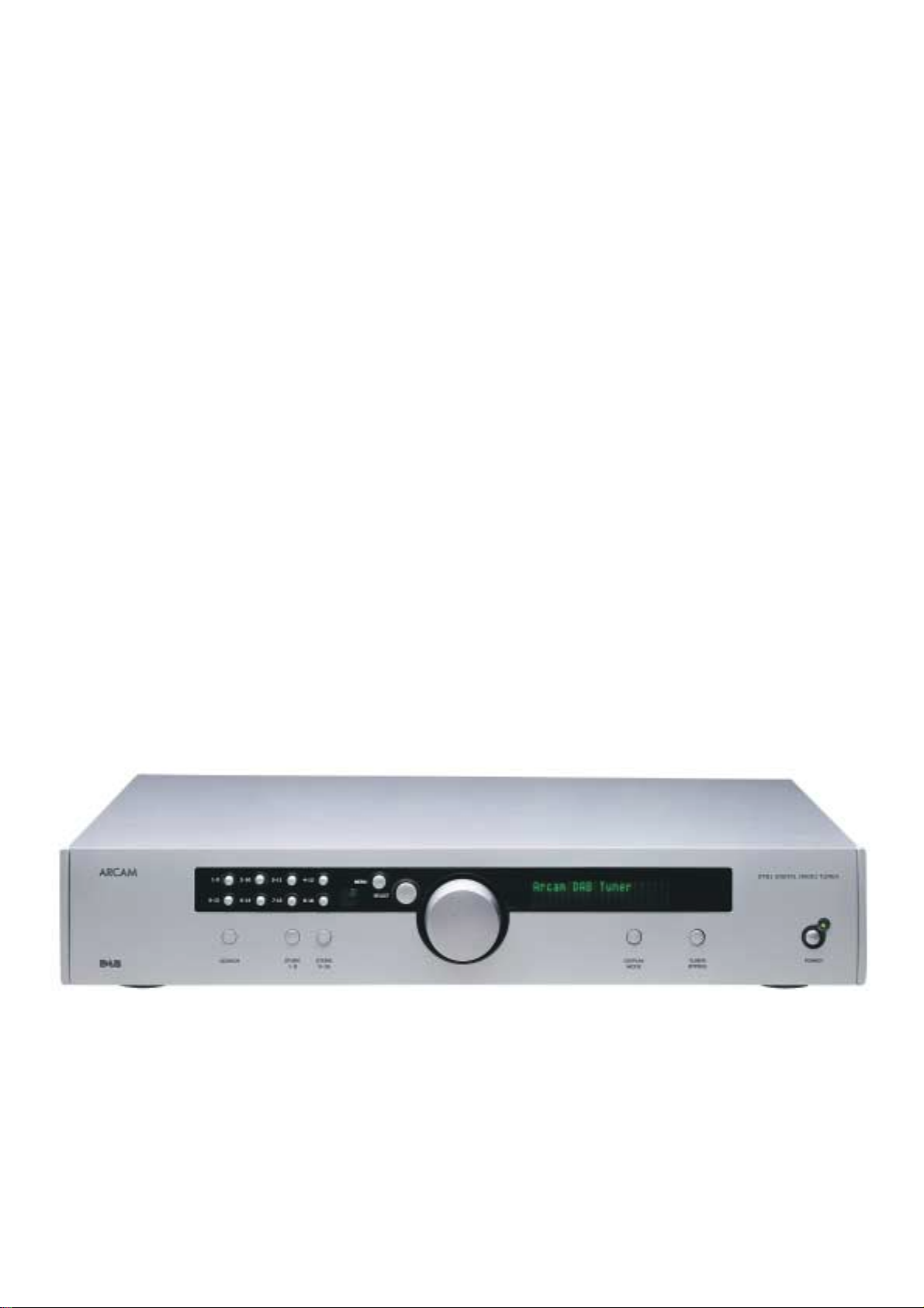
Service Manual
ARCAM
DiVA DT81
Digital Radio Tuner
DT81
Issue 1.0
ARCAM
Page 2

Contents List
!
Contents list
!
Circuit description
!
Service guide
!
Circuit diagrams
!
Component overlays
!
Circuit board parts list
!
General assembly parts list
Page 3

DT81 Circuit Description
Summary
The L918 forms the basis of the DT81 DAB tuner. All the circuitry
of the tuner is on the same board, with the exception of the front
panel PCB.
The tuner is based on the Roke Manor gold card which provides the
RF receiver and DAB decoding. To accompany this module the DAB
motherboard has various power supplies, a Hitachi H8
microcontroller, a D- A converter with output bu ffer, and an SPDIF
transmitter.
Power supplies and muting
The mains transformer T1 is used for 230V and 115V operation, the
voltage selection is done by fitting different fuses. F1 160mA is
fitted for 230V and F2 250mA for 115V.
The front panel board is powered from the 7.5V unregulated supply
(it has its own regulator). The digital supplies are switched by SW3,
while the an alogue supplies are on all the t ime while the mains is
connected.
Regulated supplies
P15V, N15V. +/-15V for the output buffer and DAC 5V regulator.
P5VDAC. +5V supply for DAC.
P5VDAB. 5V supply for DAB module.
P5V. +5V supply for digital circuits - Micro and SPDIF transmitter.
P10V. +10V supply for DAB module.
P7V5_UR. Unregulated 7.5V supply goes to front panel.
Z9 is a Toshiba TA7317. This controls the muting/bypass relay. The
same relay is used for power on/off muting and also FM tuner bypass
mode.
The muting circu it has a time constant of 2.5 seconds, s o there is
always a 2.5 second delay when un-muting the output.
The FM tuner bypass switch is shown on this sheet (SW2) and is
accessed from the front of the unit.
Micro, DAB module, SPDIF
Z204 is a Hitachi H8/3 048F 16 bit microcontroller. It has FLASH
program memory, and is programmed via header SK1. Z202 is a
64kbit parallel EEPROM used for storing multiplex data. this is
where the s ystem stores d ata about th e multiplexes it finds when it
does a search, and other i nformati on (presets, comp ression level, sort
type, display mode).
Z205 is a 3 pin reset generator IC. SW1 is a latching push switch
accessed from the rear of the unit. If the switch is pushed in,
RDI_ON will be low. This has the effect of removing data services
from the list of services. If the switch is left out, RDI_ON will be
high and the data services can be seen.
SK3 is used to connect to the front panel, communication is done via
the I2C bus. Power for the front panel comes in the form of
P7V5_UR. Note that although P5V connects to the front panel, it is
not used for power. Its purpose is to light the front panel LED green.
DAB module: JP1 is a 50 way SAMTEC connector which provides
the interface to the Roke DAB module. All the I/O to the module is
on this conn ector a part from t he a erial i npu t whic h ha s a cab le goin g
straight from the rear panel to the module.
Communication between the micro and the DAB module is done via
the serial port of eac h device on TX_DAB/RX_DAB.
The digital audio output from the module comprise of MCLK
(12.288MHz mast er clock), LRCK (48kHz left/right clock), SCLK
(serial data clock) and SDATA (serial data).
These signals go to the D-A converter, and also to the SPDIF
transmitter Z201.
Z201 is the SPDIF transmitter. Each one of the differential ouputs is
used separately. SPDIF_OP is for the opt ical output, SPDIF_CX is
for the coax output.
DAC
Z101 is a CS4327 D-A converter, followed by filter/buffer Z102.
This is followed by ac coupling capacitors. The relay RLY1 is the
last stage before the phono output connectors. 2 stereo outputs are
provided on SK101. SK102 is an input which gets routed through the
relay when the relay is off.
An external FM tuner can be connected to this, in order to avoid
taking up an ext ra input on the amp lifier. Wh en the t uner is off or i n
bypass mode, the FM tuner is routed to the output.
The digital aud io outputs are also shown on this sheet. TX101 and
associated compon ents provid e an i solated unba lanc ed SPDIF ou tpu t
on SK103, and Z4 produces an optical output.
Software notes
The system ha s non volatile storag e in the form of th e EEPROM,
Z202. The fo llowing in formation i s stored th ere and is reme mbered
at power up:-
Service data - all the IDs and static prog types of the services
available in the ensembles found in the last search. This is the
information viewed when turn ing the knob.
Service selected - last service selected.
Display mode - prog type, dynamic label, data rate or signal quality.
Display brightness - off, dim or bright.
Compression level - off or 1-5.
The following parameters are NOT remembered:Engineering mode. If the unit is turned off while in engineering
mode (or test mode), it will default back to user mode on power up.
Bypass mode - the unit will always power up not in bypass mode.
Secondary services - if a secondary service is selected when it is
switched off, it will power up with the parent service selected.
Erasing the E EPROM - to erase th e EEPROM, go into engin eering
mode (SELECT +8), then hold down preset buttons 1,4,5,8. The
display will say ‘ERASING EEPROM’ followed by ‘PASSED
EEPROM TEST’ then ‘EEPROM ERASED’. If you switch the
power off and on again , it will c om e on with a ll th e p arameters res et.
Display mode - prog type
Display brightness - bright
Compression - off.
Selection Mode – m an ual
Test mode
If you hold in the bypass button while powering up, this will put the
unit in test mode. When the bypass button is released, the software
version will be displayed. Pressing the front panel buttons will cause
a message to be displayed. Turning the knob clockwise or
anticlockwise will cause a message to be displayed. Any RC5 remote
commands will also be displayed, with command and system codes,
and an asterisk for the toggle bit.
Fault mode
On switch on if the Roke module is not fitted, or if there is a problem
with the RX or TX communication signal between the module and
the H8, the unit displays ‘ERROR CIP FAILURE’.
Page 4
DT81 Service Guide
Fault diagnostics
Fault Action
No power Check mains fuse
Check power supply rails
No Audio output Check for digital output
Check analogue power supply voltages
Check DAC IC
Fails to respond to commands Check supply voltages
Check DAB module
No Display Check flex foil cable
Check for dry joints on micro and display
Spurious display readout Check for dry joints on display board
Display reads “ERROR CIP FAILURE” DAB module not communicating with main micro – replace
DAB module
Display reads “NO SERVICE FOUND” DAB module not receiving signal – check connections to
DAB module/ replace DAB module
Power supply test points
Position Voltage
TP1 0 volt reference
TP2 +5 volts - DAB module
TP3 +10 volts - DAB module
TP4 +5 volts - DAC
TP5 +15 volts
TP6 -15 volts
TP7 +5 volts
Hints & tips
!
No analogue signal - measure between the junction of D10, D11 and D8, D9 for the
secondary supply feed from the transformer, this should be 40 VAC. If this is low or missing
the transformer will require replacing.
!
Not responding to front panel controls – check the processor is ok by pressing the bypass
button, if the bypass relay functions then check the DAB module supplies are ok. If ok then
replace the DAB module.
!
Please note that there are no serviceable parts within the DAB module.
Page 5

87654321
D
PSU & Remote
L918C2_1.1.SCH
REMOTE_BUS BYPASS
BP STBYLED
C
DAC and o/p amp
L918C4_1.1.SCH
SPDIF_CX MCLK
LRCK SCLK
REMOTE_BUS
BP
SPDIF_OP
SDATABYPASS
STBYLED
Micro and Gold Card I/F
L918C3_1.1.SCH
LRCK
MCLK
SCLK
SDATA
SPDIF_CX
SPDIF_OP
FD_1
FIDUCIAL
FD_2
FIDUCIAL
FD_3
FIDUCIAL
FD_4
FIDUCIAL
PCB
PCB
D
C
DD3
Update Box
UPDATE_BOX
1 4Sheet of
L918PB_1
DRAWING NO.
B
A
ISSUE
L918C1
Tooling & Fixing Holes
Tooling Holes
B
FIX11
FIXING HOLE 3.5
CLEARANCE HOLE
DD4
Layout by
Cliff
CLOGO
A
1 2 3 4 5 6 7 8
DRAWING TITLE
DIVA DT81 DAB Tuner - Project Sheet
Circuit Diagram
A & R Cambridge Ltd.
Pembroke Avenue
Denny Industrial Centre
Waterbeach
Cambridge CB5 9PB
Notes:
Filename
J:\ECO_wip\01_1106 new 1.7 roak module\L918_1.1\L918_1.1.DDB - L918c1_1.1.prj
01_1076
ECO No. DESCRIPTION OF CHANGE
INITIALS
Date Printed
Main PCB Fixing Holes
FIX5
FIX1
FIXING HOLE 3.5
FIXING HOLE 3.2
FIX6
FIX7
FIXING HOLE 3.5
FIXING HOLE 3.5
CHS4
F3
T100MASP
FIX3
FIX2
FIXING HOLE 3.2
CHS2 CHS3
FIX8
FIXING HOLE 3.5
FIX4
FIXING HOLE 3.5
FIXING HOLE 3.5
FIX10
FIX9
FIXING HOLE 3.5
FIXING HOLE 3.5
Kit Mask
FOR DT81 DAB TUNER EXCLUDE NF,DT81
PG 8/6/01 ROKE MODULE V1.7 + changed R67 & R68 1.101_1106
CL 19/03/01 PRODUCTION RELEASE 1.0
CL 22/01/01 PROTOTYPE (NEW DAC & TOSLINK) B.0
CL 03/10/00 INITIAL PROTOTYPE A.0
DATE
Drawn by:
CL11-Jun-2001
Page 6

SW3D
DAB Module
12
11
D
C
B
(NOT FITTED ON DT81, USES SWITCH ON DISPLAY BOARD)
A
10
A1014
SK4 IEC2
LIVE1 NEUT1
LIVE NEUT
1
2
LIVE2
C60
470P NPO 0805
C65
470P NPO 0805
EMCGND
FM Tuner Pass-through
3
2
SW2A
1
2PCO_NON_LAT
1 2 3 4 5 6 7 8
NL
C31
T2
CM_CHOKE
3 4
F2
!
WARN
T250MA115V
115V units only
F1
!
WARN
T160MA
230V units only
C64
470P NPO 0805
C61
470P NPO 0805
SW2B
2PCO_NON_LAT
220N X2 CLASS
NEUT2
Analogue and
Digital grounds
are joined at the
DAC, Z10
NEUT2
AC115V
115V
AC230V
230V
MUTE CIRCUIT
P5V
6
5
4
R77
10K 0805
0V
T3
115V
230V
C35
1U0 EL
SK12
R26
0R0 0805
T1
1
2
8
7
5
6
12
T2
11
L848TX
+
BYPASS
IDC4S
BP
P7V5_UR
1
2
3
4
14
18V
13
19
0V
20
18V
16
7V5
15
21
22
18
12V
17
23
24
SW3B
A1014
P5V
ACDIG1
T4
ACDIG2
0V
ACDIG3
T1
ACDIG4
0V
R30
10K 0805
R33
10K 0805
R34
47K 0805
ACAUD1
ACAUDG1
ACAUD2
ACDIG1
ACDIG2
ACDIG3
ACDIG4
6
5
4
R71
10K 0805
SK6
1
2
3
4
5
6
7
8
9
10
FFC10V
ACAUD2
R24
1K8 0805
D16
UF4003
R32
47K 0805
TA7317P
R70
47K 0805
D10
UF4003
D8
D12
D14
UF4003
GND1
Z9
2
3
+UR
-UR
ACAUD1
UF4003
UF4003
D6
UF4003
D19
UF4003
IN1
IN2
-UR
P15V
MUTE1
N15V
R29
47K 0805
1
PWR
V-
5
R12
8K2 0805
UF4003
D15
C32
10N 0805
R31
47K 0805
8
RC
0V
4
AGND1
D11
UF4003
D9
UF4003
SW3A
A1014
D13
UF4003
D7
UF4003
D20
UF4003
C23
+
100U EL
9
V+
FB
7
R27
33K 0805
O
C34
+
1U0 EL
R73
1R0 FU
3
2
1
+UR
MUTE1
6
R28
47K 0805
R62
1R0 FU
10N 0805
C59
CHS2
R13
8K2 0805
P3
SW3C
A1014
R74
1R0 FU
POWER SUPPLIES
WARN
!
R72
1R0 FU
WARN
!
R21
1R0 FU
P2
+
C10
3M3 EL
R76
22R 0805
9
8
7
P9
D17
1N4148
MUTE1
PUNREG1
R20
1R0 FU
P7V5_UR
Connect ground to chassis fixing
via decoupling capacitor C32.
P8
+
STBYLED
P15V
R25
100R 0805
3R3 FU
C37
+
1M0 35V
C39
+
1M0 35V
3R3 FU
TO220HS30REG
C29
3M3 EL
RLY1C
RLY 51SB12T
!
WARN
R18
!
WARN
R19
NUNREG1
Z1 LM317T
I
HS1A
C38
1M0 35V
C40
1M0 35V
-UR
Vin
EMCGND
SK5A
Near to PCB
JACK3.5X2
+UR
C36
100P NPO 0805
+
A
+
ADJ
+
C62
1N0 PP
C63
1N0 PP
I
D2
1N4003F
Vout
C11
10U EL
REMIN1
REMIN2
Z3 LM317T
I
Vin
A
Vin
Z5 LM337T
O
R17
390R 0805
R58
2K7 0805 0.1%
SK5B
JACK3.5X2
EMCGND
ADJ
A
+
C21
100U EL
+
C22
100U EL
ADJ
Vout
1N4003F
Far from PCB
C42
100P NPO 0805
DRAWING TITLE
DiVA DT81 DAB Tuner - Power Supplies & Muting
Circuit Diagram
A & R Cambridge Ltd.
Pembroke Avenue
Denny Industrial Centre
Waterbeach
Cambridge CB5 9PB
Notes:
Filename
J:\ECO_wip\01_1106 new 1.7 roak module\L918_1.1\L918_1.1.DDB - L918C2_1.1.SCH
D5
1N4003F
Vout
D4
C26
+
220U EL
P10V
TP5
O
O
TP3
TEST_POINT
+
C19
100U EL
R41
1K0 0805
TEST_POINT
R56
220R 0805
R54
2K4 0805 1%
R55
2K4 0805 1%
+
R57
220R 0805
TP6
TEST_POINT
Z7 7805
I
Vin
GND
G
HS2A TO220HS08REG
Supply +10V
R44
4K7 0805
R42
1K0 0805
P15V
P15V
C12
+
100U EL
C13
100U EL
N15V
N15V
Vout
HS
R49
100K 0805
680P PP
D18
4V7 400MW
DAC
Supply
Z2 LM317T
I
Vin
HS3A
TO220HS30REG
Z8 7805
I
Vin
R4
10K 0805
QQ2
QPAD
R50
100K 0805
R5
10K 0805
QQ1
QPAD
O
C41
+5V for DAB
TP2
TEST_POINT
+
TP1
TEST_POINT
C50
10N 0805
P5VDAB
C24
220U EL
L1
27MH
QQ3
QPAD
P15V
!
WARN
C20
1M0 25V
R3
10K 0805
3
2
R52
1K8 0805
R51
1K5 0805 1%
R53
1K8 0805
R22
100R 1W CF
+
+
C27
220U EL
Z10A
LM393A SM
470P NPO 0805
QQ5
QPAD
C33
10N SM
1
C55
PG 8/6/01 1.101_1106 ROKE MODULE V1.7 + changed R67 & R68
01_1076
CL 19/03/01 PRODUCTION RELEASE 1.0
CL 22/01/01 PROTOTYPE (NEW DAC & TOSLINK B.0
CL 03/10/00 INITIAL PROTOTYPE A.0
ECO No. DESCRIPTION OF CHANGE
INITIALS
Date Printed
DATE
Drawn by:
CL11-Jun-2001
A
G
QQ4
ADJ
+
GND
QPAD
D3
1N4003F
Vout
C14
10U EL
Vout
2 4Sheet of
O
O
P5V
Z10B
6
5
LM393A SM
LM393A SM
TEST_POINT
R16
330R 0805
R43
1K0 0805
+5V for micro
TP7
TEST_POINT
+
7
Z10C
DRAWING NO.
TP4
+
P5V
P7
C28
100U EL
R6
10K 0805
84
87654321
P5V DAC
P5
C25
22U EL
REMOTE_BUS
P5V
C51
10N 0805
L918C2
D
C
B
A
ISSUE
Page 7

87654321
1
S/PDIF Transmitter
1
C7/C3
2
PRO
3
C1/FC0
4
C6/C2
5
MCK
6
SCK
7
FSYNC
8
SDATA
9
V
10
C/SBF
11
U
12
C9/C15
L5
1U0H SM
CHS3
100P NPO 0805
100P NPO 0805
CHS3
RDI Interface
I/P
Z201
CS8402A
Q4
ZVNL120
C49
Q1
ZVNL120
P5V
23
VCC
GND
C3
10N 0805
CS8402A
R78
100R 0805
C72
47P NPO 0805
C46
FPRESET
Z203
GP1FA550TZ
C4
10N 0805
TRNPT/FC1
M2
M1
M0
TXP
Vd+
Gnd
TXN
RST
CBL/SBC
EM0/C9
EM1/C8
C45
100P NPO 0805
C47
100P NPO 0805
C48
100P NPO 0805
CHS3 CHS3
C5
10N 0805
24
23
22
21
20
19
18
17
16
15
14
13
P7V5_UR
C54
100P NPO 0805
L4
33UH AX
R69
10R 0805
123
LK1
MOLEX3MV
DISPGND
P5V
nREQ
C53
CHS3
100P NPO 0805
R67
100R 0805
nReset
MCLK
LRCK
SCLK
SDATA
REMOTE_BUS
STBYLED
P7V5DISP
SCL
C52
100P NPO 0805
P5V
R68
330R 0805
SDA
SPDIF_OP
SPDIF_OP
nREQ
BYPASS
SPDIF_CX
To Display PCB
SK3
1
2
3
4
5
6
7
8
9
10
11
12
13
14
15
16
17
18
19
20
21
22
FFC22V
SK8
1
2
IDC2S
SK9
1
2
3
4
5
6
IDC6S
SK10
1
2
3
4
5
IDC5S
D
C
B
DAB Module Connector
VPLL1
GNDMOD
P10V
SCL
SDA
Z204
75
74
73
72
71
70
69
68
67
66
65
64
63
62
61
60
59
58
57
56
55
54
53
52
51
H8/3048F
SCL
SDA
THIEF2
JP1
49 50
47 48
45 46
43 44
41 42
39 40
37 38
35 36
33 34
31 32
29 30
27 28
25 26
23 24
21 22
19 20
17 18
15 16
13 14
11 12
9 10
7 8
5 6
3 4
1 2
50 W SKT
R1
10K 0805
VPLL
TXD_DAB
RXD_DAB
84
85
86
AVss
P7.7/AN7/DA1
_VPLL
TEST_POINT
R40
33R MF
R45
33R MF
C44
10N 0805
80
81
82
83
P7.3/AN3
P7.4/AN4
P7.5/AN5
P7.6/AN6/DA0
R15
2K2 0805
78
79
P7.0/AN0
P7.1/AN1
P7.2/AN2
TEST_LOOP
P9V9
C43
10N 0805
76
77
Vref
AVcc
MD2
MD1
MD0
P6.6/LWR
P6.5/HWR
P6.4/RD
P6.3/AS
XTAL
EXTAL
NM1
RES
STBY
CLKOUT
P6.2/BACK
P6.1/BREQ
P6.0/WAIT
P5.3/A19
P5.2/A18
P5.1/A17
P5.0/A16
P2.7/A15
P2.6/A14
50
THIEF1
P5V
Vcc
Vss
Vss
CHS2 CHS3
Z6B
4
D
P5V
C6
10N 0805
C
B
Decoupling for ICs
C7
10N 0805C810N 0805C910N 0805
Z204Z202 Z203 Z205
SW1A
56SW1B
4
2PCO
2PCO
5
9
10
12
13
BYPASS
P5V
R2
3
10K 0805
2
1
74HC32 SM
Z6C
74HC32 SM
Z6D
74HC32 SM
RDI_ON
C18
10N 0805
BYPASS
6
8
11
nReset
MD
7
BYPASS
14
Z6E
GND
VDD
74HC32 SM
MD
BP
SK1
1 2
3 4
5 6
7 8
9 10
11 12
13 14
HEADER 7X2
Reprogramming Interface
P5V
PMODE
TXD1
RXD1
P5V
P_mode
R39
2K2 0805
C66
470P NPO 0805
VPP
C67
470P NPO 0805
SK2
1
2
3
4
5
IDC5S
P5V
10
11
12
13
14
15
16
17
18
19
20
21
22
23
24
25
THIEF4
C68
470P NPO 0805
PA4
PA5
PA6
PA7
1
Vcc
2
PB0
3
PB1
4
PB2
5
PB3
6
PB4
7
PB5
8
PB6
9
PB7
Vpp/RESO
Vss
TxD0/P9.0
TxD1/P9.1
RxD0/P9.2
RxD1/P9.3
IRQ4/SCK0/P9.4
IRQ5/SCK1/P9.5
D0/P4.0
D1/P4.1
D2/P4.2
D3/P4.3
Vss
D4/P4.4
D5/P4.5
D6/P4.6
nREQ
P5V
R10
10K 0805
M1
DAB TUNER MODULE
C69
DAB TUNER MODULE
470P NPO 0805
R65
100R 0805
R66
100R 0805
P10V
L3
2U2H AX
P5V P5V
R14
2K2 0805
Q2
ZVNL120Q3ZVNL120
87
88
89
90
91
100
92
Vss
PA093PA194PA295PA396PA497PA598PA699PA7
P8.4/CS0
P8.0/IRQ0
P8.1/IRQ1
P8.2/IRQ2
P8.3/IRQ3
H8/3048F
D7/P4.726D8/P3.027D9/P3.128D10/P3.229D11/P3.330D12/P3.431D13/P3.532D14/P3.633D15/P3.734Vcc35A0/P1.036A1/P1.137A2/P1.238A3/P1.339A4/P1.440A5/P1.541A6/P1.642A7/P1.743Vss44A8/P2.045A9/P2.146A10/P2.247A11/P2.348A12/P2.449A13/P2.5
THIEF3
D0D1D2D3D4D5D6
D7
R46
100R 0805
RDI
SCLK
SDATA
R60
1K0 0805
LRCK_IN
R64
100R 0805
RESET
MCLK
P5VDAB
L2
2U2H AX
P5VDAB
Z6A
1
2
MD
C2
3
74HC32 SM
P5V
C17
10N 0805
R9
10K 0805
D1
BAS16W SM
X1
16MHZ#A
22P NPO 0805C122P NPO 0805
R48
1K0 0805
nReset
P5V
R7
10K 0805
SK11
IDC2S
R47
330R 0805
P5V
R75
10K 0805
nReset
1
2
RBUSFP
Z205
DS1233
DS1233M
R61
100R 0805
MCLK_SP
R63
100R 0805
REMOTE
1
2
Vcc
Vcc
Res
Gnd
LRCK
3 5
P5V
2
4
3
1
100P NPO 0805
C70
C71
100P NPO 0805
Z11
4
74AHC1G00 SM
D0D1D2D3D4D5D6
P5V
28
VCC
EEPROM
A
Z204SW
L918SW
DT81 H8 SOFTWARE
L918SW
1 2 3 4 5 6 7 8
D7
1
26
19
RB
M28C64A
DQ011DQ112DQ213DQ315DQ416DQ517DQ618DQ7
A010A19A28A37A46A55A64A73A825A924A1021A1123A12
A1A0A2A3A4A5A6A7A8A9A10
NC
2
A11
A12
VSS
WE27CE20OE
P5V
Z202
14
22
A0A1A2A3A4A5A6A7A8A9A10
A11
A12
A
DRAWING TITLE
DiVA DT81 DAB Tuner - micro circuit
A & R Cambridge Ltd.
Pembroke Avenue
Denny Industrial Centre
Waterbeach
Cambridge CB5 9PB
Notes:
Filename
J:\ECO_wip\01_1106 new 1.7 roak module\L918_1.1\L918_1.1.DDB - L918C4_1.1.SCH
Circuit Diagram
PG 8/6/01 1.101_1106 ROKE MODULE V1.7 + changed R67 & R68
CL 19/03/01 PRODUCTION RELEASE 1.0
01_1076
CL 22/01/01 PROTOTYPE (NEW DAC & TOSLINK) B.0
CL 03/10/00 INITIAL PROTOTYPE A.0
INITIALS
11-Jun-2001
DATE
Drawn by:
CL
3 4Sheet of
DRAWING NO.
ECO No. DESCRIPTION OF CHANGE
Date Printed
L918C4
ISSUE
Page 8

D
C
B
A
LRCK
SDATA
SCLK
MCLK
+
C110
10U EL
C118
100N 0805
+
C111
10U EL
84
Z104C
4560D SM
DIGITAL OUTPUT
SPDIF_CX
AUDIO AMPLIFIER AND LOW-PASS FILTER
VOUTLP
VOUTLN
VOUTRP
VOUTRN
LEFT1
20K LOG SNAPIN#A
AUDGND
Z4
GP1FA550TZ
R102
5K6 0805 1%
R100
5K6 0805 1%
R104
5K6 0805 1%
R103
5K6 0805 1%
C123
10U NP
RV1A
RIGHT1
20K LOG SNAPIN#A
C100
2N2 PP
C101
2N2 PP
C102
2N2 PP
C104
2N2 PP
C124
10U NP
RV1B
DRAWING TITLE
DiVA DT81 DAB Tuner - DAC, Audio Outputs & Headphones
A & R Cambridge Ltd.
Pembroke Avenue
Denny Industrial Centre
Waterbeach
Cambridge CB5 9PB
R23
22R 0805
R101
22R 0805
1
2
3
4
5
6
7
C133
10U SILMIC
+
C120
100N 0805
C119
100N 0805
84
Z103C
4560D SM
SPDIF_CX
R146
100R 0805
1 2 3 4 5 6 7 8
8
9
10
11
12
13
14
P15V
C115
680P PP
C116
680P PP
N15V
SPDIF_OP
C127
100P NPO 0805
Z100
LRCIN
DIN
BCKIN
MODE8X
SCLK
DIFFHW
DGND
DVDD
AVDDR
AGND2R
VMIDR
VOUTRN
VOUTRP
AGND1
WM8740
R147
10K 0805
P5V DAC
DAC
WM8740
MC/DM1
MD/DM0
AGND2L
VOUTLN
VOUTLP
C128
DIGOUTP1
100N 0805
C129
100N 0805
+
C103
100U SILMIC
28
ML/IIS
27
26
25
MUTE
24
MODE
23
CS/IWO
22
RST
21
ZERO
20
AVDDL
19
18
VMIDL
17
16
15
Vcc
Z102C
OPA2134PA SM
SK103
PHONO1
EMC
R145
0R0 SM
SPDFGND
DIGOUTN1
C135
1N 0805
CHS2
C132
C121
100N 0805
C122
100N 0805
P15V
N15V
+
C113
680P PP
C114
680P PP
C16
10N 0805
C134
10U SILMIC
+
+
C117
10U EL
1
P5V
23
VCC
I/P
GND
100N 0805
84
C15
22U EL
R110
1K5 0805 1%
R105
6K8 0805 1%
R109
1K5 0805 1%
R106
6K8 0805 1%
R114
1K5 0805 1%
R107
6K8 0805 1%
R113
1K5 0805 1%
R108
6K8 0805 1%
C105
470P PP
C107
470P PP
Notes:
Filename
J:\ECO_wip\01_1106 new 1.7 roak module\L918_1.1\L918_1.1.DDB - L918C3_1.1.SCH
Z102B
5
6
3
2
C57
100U NP
7
OPA2134PA SM
C106
470P PP
Z102A
1
OPA2134PA SM
C109
470P PP
R37
0R0 0805
R129
2K2 0805
R35
100K 0805
C58
100U NP
R36
100K 0805
Circuit Diagram
LEFT1
LEFT1
RIGHT1
RIGHT1
R137
2K2 0805
P15V
P15V
R130
12K 0805
2
3
R132
2K2 0805
Not Fitted
R115
4K7 0805 1%
C108
+
100U SILMIC
Not Fitted
R116
4K7 0805 1%
C112
+
100U SILMIC
1
Z103A
4560D SM
R138
12K 0805
Z104A
2
3
4560D SM
R140
2K2 0805
SK102
1
F
EMC
N
PHONO2#
SH101
1
F
PHONO4G
N
HEADPHONE AMPLIFIER
HPSL
F
SK101A
N
PHONO4G
EMCPHONO2
C131
47P NPO 0805
C125
100P PP
CHS4
ALL PARTS IN THIS BOX ARE NOT FITTED ON DT81
ANGND
5
6
R111
4K7 0805 1%
R122
75R 0805 1%
R121
4K7 0805 1%
R133
22R 0805
Z103B
4560D SM
R134
12K 0805
1
Z104B
5
6
R112
75R 0805 1%
7
R141
22R 0805
7
4560D SM
R142
12K 0805
R135
22R 0805
HPGnd
LTUNIN
RLY1A
RLY 51SB12T
L101
7F003
1N 0805
RTUNIN
RLY1B
RLY 51SB12T
R143
22R 0805
LOUT
OPGND
SK101B
C30
ROUT
R136
100R 1W CF
HPSR HPSE
R144
100R 1W CF
PG 8/6/01 1.101_1106 ROKE MODULE V1.7 + changed R67 & R68
01_1076
ECO No. DESCRIPTION OF CHANGE
Date Printed
CL 19/03/01 PRODUCTION RELEASE 1.0
22-01-01 PROTOTYPE (NEW DAC & TOSLINK) B.0
CL
CL
03/10/00 INITIAL PROTOTYPE A.0
INITIALS
DATE
Drawn by:
CL/PG11-Jun-2001
4 4Sheet of
LEFT
RIGHT
C130
47P NPO 0805
LEFT
EMC
RIGHT
EMC Shield
C126
100P PP
C73
1N 0805
DRAWING NO.
EMCGND
4
5
2
3
1
6
7
EMCGND
L
LHC
RHC
R
87654321
SK7
1 2
3 4
5 6
DIL6 VPLG
SK104
HPSKT
L918C3
D
C
B
A
ISSUE
Page 9

Page 10

Page 11

DT81 Display Board L919_1.1
Reference Description Part
C1 CERD 100N 63V 20% RA 2A410
C2 ELST 220U 16V 2N722
C3-C5 CERD 100N 63V 20% RA 2A410
C6,C6 ELST 220U 16V 2N722
C8 CERD 100N 63V 20% RA 2A410
C9-C19 CERD 1N0 63V 20% RA 2A210
D1-D14 SSDIODE 1N4148 75V 3A4148
LED100 LED RED/GREEN 3MM L-
M1 NORITAKE ITRON
PCB PRINTED CIRCUIT BOARD L919PB_1
Q1 TRANS LF SS P BC557B 4A557
Q2 TRANS MOSFET SW
R1 RES MF W4 150R 1% 1H115
R2 RES MF W4 1% 1K0 1H210
R3 RES MF FU W3 3R3R 5%
R4,R5 RES MF W4 4K7 1% 1H247
R6,R7 RES MF W4 10K 1% 1H310
R8,R9 RES MF W4 4K7 1% 1H247
R10 RES MF W4 10K 1% 1H310
R11-R13 RES MF W4 100R 1% 1H110
RP1 RES NETWORK 100Kx8
RX1SP IR RX SUPPORT PAD E822AP
RX1 REMOTE RX PIC-26043TM2
SK1 22-WAY FFC CONN HORIZ 8K8122
SW1SW15
SW16 EC16B2414 A1211
X1 CER RESON 4.00MHz 7W005
Z1 IC VREG POS 7805 5D7805
Z2SW DT81 DISPLAY SOFTWARE L919SW
Z2 40 PIN IC SOCKET 8S040
Z2 IC CMOS MICRO PIC16C65 5H16C65
93WEGW
CU20025RCPB-U1J
ZVNL120A
NFR25
COMMON
38KHZ
TACT SWITCH 2-PIN LOW
PROF 9.5mm ACTUATOR
SKHVPH
Number
3D006
B1010
4K120
1G833
1V410
B2107
A1508
DT81 Main Board L918_1.1
Reference Description Part
C1,C2 MLC 22P 100V NPO 5% 0805 2L022
C3-C9 MLC 10N 50V X7R 10% 0805 2J310
C10 ELST 3M3 25V 2N833
C11 ELST 10U 50V 2N610
C12,C13 ELST 100U 25V 2N710
C14 ELST 10U 50V 2N610
C15 ELST 22U 63V 2N622
C16-C18 MLC 10N 50V X7R 10% 0805 2J310
C19 ELST 100U 25V 2N710
C20 ELST 1M0 25V 2N810
C21-C23 ELST 100U 25V 2N710
C24 ELST 220U 16V 2N722
C25 ELST 22U 63V 2N622
C26,C27 ELST 220U 16V 2N722
C28 ELST 100U 25V 2N710
C29 ELST 3M3 25V 2N833
C30 MLC 1N 50V X7R 10% 0805 2 J 210
C31 220NF CLASS X2 CAP
275VRMS
Number
2D422
C32 MLC 10N 50V X7R 10% 0805 2J310
C33 MLC 10N 50V X7R 10% SM 2C310
C34,C35 ELST 1U0 50V 20% RA 2N510
C36 MLC 100P 100V NPO 5% 0805 2L110
C37-C40 ELST 1M0 35V 2N810C
C41 PPRO 680P 5% 63V RA 2D168
C42 MLC 100P 100V NPO 5% 0805 2L110
C43,C44 MLC 10N 50V X7R 10% 0805 2J310
C45-C49 MLC 100P 100V NPO 5% 0805 2L110
C50 MLC 10N 50V X7R 10% 0805 2J310
C51 MLC 10N 50V X7R 10% 0805 2J310
C52-C54 MLC 100P 100V NPO 5% 0805 2L110
C55 MLC 470P 100V NPO 5% 0805 2L147
C59 MLC 10N 50V X7R 10% 0805 2J310
C60,C61 MLC 470P 100V NPO 5% 0805 2L147
C62,C63 PPRO 1N0 5% 63V RA 2D210
C64-C71 MLC 470P 100V NPO 5% 0805 2L147
C72 MLC 47P 100V NPO 5% 0805 2L047
C73 MLC 1N 50V X7R 10% 0805 2J210
C100C102
C103 ELEC 100U 25V SILMIC 2P710AS
C104 PPRO 2N2 5% 63V RA 2D222
C105C107
C108 ELEC 100U 25V SILMIC 2P710AS
C109 PPRO 470P 63V 5% RA 2D147N
C110,C111 ELST 10U 50V 2N610
C112 ELEC 100U 25V SILMIC 2P710AS
C113,C114 PPRO 680P 5% 63V RA 2D168
C117 ELST 10U 50V 2N610
C118C122
C127 MLC 100P 100V NPO 5% 0805 2L110
C128,C129 MLC 100N 50V X7R 10% 0805 2J410
C130,C131 MLC 47P 100V NPO 5% 0805 2L047
C132 MLC 100N 50V X7R 10% 0805 2J410
C133,C134 ELEC 10U 25V SILMIC 2P610CS
C135 MLC 1N 50V X7R 10% 0805 2J210
D1 DIODE SS SM BAS16W 3AS16W
D2-D5 RECTIFIER 1N4003F 1A 200V 3B4003
D6-D16 ULTRAFAST RECTIFIER
D17 SSDIODE 1N4148 75V 3A4148
D18 ZENER 4V7 400MW 3C04704
D19,D20 ULTRAFAST RECTIFIER
F1 FUSECLIP C11166
F1 FUSEHOLDER 20mm PCB 8S004
F1 INS COVER PCB
F2 FUSEHOLDER 20mm PCB 8S004
F2 INS COVER PCB
F3 FUSECLIP C11166
F3 SPARE FUSEHOLDER F062
HS1 HEATSINK TO220 CLIP 30 F007
HS2 HEATSINK TO220 8.6
HS2 HEATSINK CLIP TO220 13/8.6
HS3 HEATSINK TO220 CLIP 30 F007
JP1 CONN 50 WAY FW-25-04-L-
L1 27mH INDUCTOR 7D327
L2,L3 2U2H INDUCTOR 7D922
PPRO 2N2 5% 63V RA 2D222
PPRO 470P 63V 5% RA 2D147N
MLC 100N 50V X7R 10% 0805 2J410
3B4003F
DIODE UF4003 1A
3B4003F
DIODE UF4003 1A
F022
FUSEHOLDER
F022
FUSEHOLDER
F008
DEGC/W
F006
DC/W
8K2001
D-350-065
Page 12

L4 33 UH IND 34-48330 7D033
L5 1UH0 IND SM NL322522T-
L101 FERRITE BEAD SINGLE
M1 DAB TUNER MODULE 1.7 B012
PCB PRINTED CIRCUIT BOARD L918PB_1
Q1-Q4 TRANS MOSFET SW
R1-R7 RES SM 0805 10K 1M310
R9,R10 RES SM 0805 10K 1M310
R12-R15 RES S M 08 0 5 8K2 1M282
R16 RES SM 0805 330R 1M133
R17 RES SM 0805 390R 1M139
R18,R19 RES MF FU W3 3R3 5%
R20,R21 RES MF FU W3 1R0 5%
R22 RES CF 1W 100R 5% 1E110
R23 RES SM 0805 22R 1M022
R24 RES SM 0805 1K8 1M218
R25 RES SM 0805 100R 1M110
R26 RES SM 0805 0R0 1M000
R27 RES SM 0805 33K 1M333
R28,R29 RES SM 0805 47K 1M347
R30 RES SM 0805 10K 1M310
R31,R32 RES SM 0805 47K 1M347
R33 RES SM 0805 10K 1M310
R34 RES SM 0805 47K 1M347
R35,R36 RES SM 0805 100K 1M410
R37 RES SM 0805 0R0 1M000
R39 RES SM 0805 2K2 1M222
R40 RES MF W4 33R 1% 1H033
R41-R43 RES S M 08 0 5 1K0 1M210
R44 RES SM 0805 4K7 1M247
R45 RES MF W4 33R 1% 1H033
R46 RES SM 0805 100R 1M110
R47 RES SM 0805 330R 1M133
R48 RES SM 0805 1K0 1M210
R49,R50 RES SM 0805 100K 1M410
R51 RES SM 0805 1K5 1M215
R52,R53 RES SM 0805 1K8 1M218
R54,R55 RES SM 0805 2K4 1M224
R56,R57 RES SM 0805 220R 1M122
R58 RES SM 0805 0.1% 2K7 1L227
R60 RES SM 0805 1K0 1M210
R61 RES SM 0805 100R 1M110
R62 RES MF FU W3 1R0 5%
R63-R67 RES SM 0805 100R 1M110
R68 RES SM 0805 330R 1M133
R69 RES SM 0805 10R 1M010
R70 RES SM 0805 47K 1M347
R71 RES SM 0805 10K 1M310
R72-R74 RES MF FU W3 1R0 5%
R75 RES SM 0805 10K 1M310
R76 RES SM 0805 22R 1M022
R77 RES SM 0805 10K 1M310
R78 RES SM 0805 100R 1M110
R100 RES SM 0805 5K6 1M256
R101 RES SM 0805 22R 1M022
R102R104
R105R108
R109,R110 RES SM 0805 1K 5 1M215
1R0J
AXIAL TAPED 2K BOX
ZVNL120A
NFR25
NFR25
NFR25
NFR25
RES SM 0805 5K 6 1M256
RES SM 0805 6K 8 1M268
7B810
7F003
4K120
1G833
1G810
1G810
1G810
R113,R114 RES SM 0805 1K 5 1M215
R121 RES SM 0805 4K7 1M247
R122 RES SM 0805 75R 1M075
R129 RES SM 0805 2K2 1M222
R130 RES SM 0805 12K 1M312
R132 RES SM 0805 2K2 1M222
R133 RES SM 0805 22R 1M022
R134 RES SM 0805 12K 1M312
R135 RES SM 0805 22R 1M022
R137 RES SM 0805 2K2 1M222
R138 RES SM 0805 12K 1M312
R140 RES SM 0805 2K2 1M222
R141 RES SM 0805 22R 1M022
R142 RES SM 0805 12K 1M312
R143 RES SM 0805 22R 1M022
R145 RES SM W4 1% 0R0 1206 1A000
R146 RES SM 0805 100R 1M110
R147 RES SM 0805 10K 1M310
RLY1 RELAY 960 OHM 51SB12T A205
SH101 PHONO EMC SHIELD E825MC
SK1 14 WAY DIL HEADER 8K6314
SK3 22-WAY FFC CONN 8K8022
SK4 IEC MAINS 2-PIN PCB 8A014
SK5 MIN JACK DUAL 3.5mm
HSJ1002-01-1020
SK101 PHONO SKT 4-WAY EMC
GOLD
SK102 PHONO SKT 2-WAY EMC 8D229
SK103 PHONO SKT SINGLE EMC 8D220
SW1 SW PUSH 2PCO A1008
SW3 SW PUSH 4PCO PBT A1014
T1 DAB TUNER TX L848TX
T2 Mains common mode choke 7E030
X1 CRYSTAL 16.MHz
PARALLEL
Z1-Z3 IC VREG POS LM317T 5D317T
Z4 SPDIF OPTICAL
TRANSMITTER
Z5 IC VREG POS LM337T 5D337
Z6 IC HCMOS SM 74HC32 5K7432
Z7 IC VREG POS 7805 5D7805
Z8 IC VREG POS 7805 5D7805
Z9 IC COMPARITOR TA7317P 5M7317
Z10 IC COMPARITOR SM DUAL
LM393A
Z11 IC AHC SN74AHC1G00 5KA100
Z100 Wolfson 192K 24bit DAC 5A8740
Z102 IC OPAMP DUAL SM
OPA2134PA
Z201 IC CMOS CS8402 SPDIF TX 5G8402
Z202 8192 X 8-BIT ELECTRICALLY
ERASABLE PROM M28C64C-
150 MS1
Z203 SPDIF OPTICAL
TRANSMITTER
Z204SW DT81 DAB TUNER
SOFTWARE
Z204 H8/3048 128K FLASH
MICROCONTROLLER
Z205 IC MICRO RESET DS1233M 5H1233
8D302
8D225
7X021
5TG550T
5M393AD
5B2134
5H2864
5TG550T
L918SW
5H3048
R111 RES SM 0805 4K7 1M247
R112 RES SM 0805 75R 1M075
Page 13

DT81 General As sembly Parts Li st
ITEM 230V 115V 100V SILVER BLACK DESCRIPTION WHERE USED QTY
L813RC REMOTE CONTROL 1
8H016 DAB AERIAL 1
E828CP E827CP COVER PLATE 1
E972AY E985AY DT81 FACIA ASSY. 1
HA4V06S HA4V06B M4X6MM SCREW COVER TO CHASSIS 4
5H16C65
B012 DAB TUNER MODULE 1.7 L918AY M1 1
C11166
160mA T
E028AY DIVA DT81 REAR PANEL ASSY 1
E806MI MAINS INSULATOR 1
E810CH CHASSIS 1
E815SP SUB PANEL 1
E859PM STORE BUTTON 8
E870PM POWER BUTTON 1
E879PM DIVA RANGE FOOT 4
E879SL PRODUCT CONFIGURATION LABEL 1
E886PM DT81 CONFIRM BUTTON 6
E891PM DIVA AMP MEDIUM KNOB PLAIN 1
E896PM SELECT BUTTON 1
F022
F062 SPARE FUSE HOLDER L918AY F3 1
F164 TAPE BK 3M TESA. 6MM WIDE 008
H026 HEX PILLAR M3X11 BRASS DAB MODULE TO MOTHERBOARD 4
HA3V06A M/C TORX P/H M3X6 ST ZP 8
HA3V10A M3 X 10 PCB TO CHASSIS 16
HE6V06B No.6 X 6 FRONT PANEL TO CHASSIS 6
HF4V09B No.4 X 9 SUB PANEL, REAR PANEL 23
HL3AB M3 WASHER BETWEEN DAB MODULE SUPPORT
K5408 LIGHT PIPE SLEEVING (6mm) 1
L801CA 22-WAY FLEX-FOIL DISPLAY MODULE TO MOTHER
L842CA AERIAL LEAD ASSEMBLY DAB MODULE TO REAR PANEL 1
L848TX DAB TUNER TX L918AY T1 1
L918AY DT81 MAIN BOARD ASSY. 1
L918SW H8 SOFTWARE L918AY Z204 1
L919AY DT81 DISPLAY BOARD ASSY. 1
E803MI DAVM PHONO SHIELD INSULATOR STICK ON EMC SHIELD BEHIND
C11256
250Ma T
INS COVER PCB FUSEHOLDER L918AY F1 F2 2
LOADED WITH L919SW
FUSE 20mm
FIT ON L919AY AT Z2 1
L918AY F1 F2 2
4
PILLARS AND PCB
1
PCB
1
PHONO SKT
 Loading...